JP4075228B2 - Manufacturing method of semiconductor device - Google Patents
Manufacturing method of semiconductor deviceDownload PDFInfo
- Publication number
- JP4075228B2 JP4075228B2JP20356199AJP20356199AJP4075228B2JP 4075228 B2JP4075228 B2JP 4075228B2JP 20356199 AJP20356199 AJP 20356199AJP 20356199 AJP20356199 AJP 20356199AJP 4075228 B2JP4075228 B2JP 4075228B2
- Authority
- JP
- Japan
- Prior art keywords
- thin film
- barrier metal
- patterning
- residue
- film resistor
- Prior art date
- Legal status (The legal status is an assumption and is not a legal conclusion. Google has not performed a legal analysis and makes no representation as to the accuracy of the status listed.)
- Expired - Fee Related
Links
Images


Classifications
- H—ELECTRICITY
- H10—SEMICONDUCTOR DEVICES; ELECTRIC SOLID-STATE DEVICES NOT OTHERWISE PROVIDED FOR
- H10D—INORGANIC ELECTRIC SEMICONDUCTOR DEVICES
- H10D86/00—Integrated devices formed in or on insulating or conducting substrates, e.g. formed in silicon-on-insulator [SOI] substrates or on stainless steel or glass substrates
- H10D86/201—Integrated devices formed in or on insulating or conducting substrates, e.g. formed in silicon-on-insulator [SOI] substrates or on stainless steel or glass substrates the substrates comprising an insulating layer on a semiconductor body, e.g. SOI
- H—ELECTRICITY
- H01—ELECTRIC ELEMENTS
- H01L—SEMICONDUCTOR DEVICES NOT COVERED BY CLASS H10
- H01L21/00—Processes or apparatus adapted for the manufacture or treatment of semiconductor or solid state devices or of parts thereof
- H01L21/02—Manufacture or treatment of semiconductor devices or of parts thereof
- H01L21/04—Manufacture or treatment of semiconductor devices or of parts thereof the devices having potential barriers, e.g. a PN junction, depletion layer or carrier concentration layer
- H01L21/18—Manufacture or treatment of semiconductor devices or of parts thereof the devices having potential barriers, e.g. a PN junction, depletion layer or carrier concentration layer the devices having semiconductor bodies comprising elements of Group IV of the Periodic Table or AIIIBV compounds with or without impurities, e.g. doping materials
- H01L21/30—Treatment of semiconductor bodies using processes or apparatus not provided for in groups H01L21/20 - H01L21/26
- H01L21/31—Treatment of semiconductor bodies using processes or apparatus not provided for in groups H01L21/20 - H01L21/26 to form insulating layers thereon, e.g. for masking or by using photolithographic techniques; After treatment of these layers; Selection of materials for these layers
- H01L21/3205—Deposition of non-insulating-, e.g. conductive- or resistive-, layers on insulating layers; After-treatment of these layers
- H01L21/321—After treatment
- H01L21/3213—Physical or chemical etching of the layers, e.g. to produce a patterned layer from a pre-deposited extensive layer
- H01L21/32133—Physical or chemical etching of the layers, e.g. to produce a patterned layer from a pre-deposited extensive layer by chemical means only
- H01L21/32134—Physical or chemical etching of the layers, e.g. to produce a patterned layer from a pre-deposited extensive layer by chemical means only by liquid etching only
- H—ELECTRICITY
- H10—SEMICONDUCTOR DEVICES; ELECTRIC SOLID-STATE DEVICES NOT OTHERWISE PROVIDED FOR
- H10D—INORGANIC ELECTRIC SEMICONDUCTOR DEVICES
- H10D86/00—Integrated devices formed in or on insulating or conducting substrates, e.g. formed in silicon-on-insulator [SOI] substrates or on stainless steel or glass substrates
- H10D86/01—Manufacture or treatment
- H—ELECTRICITY
- H01—ELECTRIC ELEMENTS
- H01L—SEMICONDUCTOR DEVICES NOT COVERED BY CLASS H10
- H01L21/00—Processes or apparatus adapted for the manufacture or treatment of semiconductor or solid state devices or of parts thereof
- H01L21/02—Manufacture or treatment of semiconductor devices or of parts thereof
- H01L21/04—Manufacture or treatment of semiconductor devices or of parts thereof the devices having potential barriers, e.g. a PN junction, depletion layer or carrier concentration layer
- H01L21/18—Manufacture or treatment of semiconductor devices or of parts thereof the devices having potential barriers, e.g. a PN junction, depletion layer or carrier concentration layer the devices having semiconductor bodies comprising elements of Group IV of the Periodic Table or AIIIBV compounds with or without impurities, e.g. doping materials
- H01L21/30—Treatment of semiconductor bodies using processes or apparatus not provided for in groups H01L21/20 - H01L21/26
- H01L21/31—Treatment of semiconductor bodies using processes or apparatus not provided for in groups H01L21/20 - H01L21/26 to form insulating layers thereon, e.g. for masking or by using photolithographic techniques; After treatment of these layers; Selection of materials for these layers
- H01L21/3205—Deposition of non-insulating-, e.g. conductive- or resistive-, layers on insulating layers; After-treatment of these layers
- H01L21/321—After treatment
- H01L21/3211—Nitridation of silicon-containing layers
Landscapes
- Engineering & Computer Science (AREA)
- Computer Hardware Design (AREA)
- Chemical & Material Sciences (AREA)
- Physics & Mathematics (AREA)
- Chemical Kinetics & Catalysis (AREA)
- Condensed Matter Physics & Semiconductors (AREA)
- General Physics & Mathematics (AREA)
- General Chemical & Material Sciences (AREA)
- Microelectronics & Electronic Packaging (AREA)
- Manufacturing & Machinery (AREA)
- Power Engineering (AREA)
- Semiconductor Integrated Circuits (AREA)
- Internal Circuitry In Semiconductor Integrated Circuit Devices (AREA)
- Weting (AREA)
- Exposure Of Semiconductors, Excluding Electron Or Ion Beam Exposure (AREA)
- ing And Chemical Polishing (AREA)
Description
Translated fromJapanese【0001】
【発明の属する技術分野】
本発明は、エッチング方法及びこのエッチング方法を用いて薄膜抵抗体を有する半導体装置を製造する方法に関し、特にタングステンあるいはその合金による配線、バリアメタル等の形成のためのエッチングに適用して好適である。
【0002】
【従来の技術】
例えば、CrSi等で構成される薄膜抵抗体の電極構造には、薄膜抵抗体とAl薄膜層との相互拡散による特性劣化を避けるため、薄膜抵抗体とAl薄膜層との間にバリアメタルをサンドイッチしたAl薄膜層/バリアメタル/薄膜抵抗体という構造が採用されている。
【0003】
バリアメタルをパターニングするに際し、バリアメタルをドライエッチングで加工すると、ドライエッチングではバリアメタルと薄膜抵抗体とのエッチング選択比を十分にとれないため、オーバーエッチ時に露出した薄膜抵抗体までエッチングされてしまう。一般的に、薄膜抵抗体は10nm程度と薄いため、薄膜抵抗体がエッチングされることが抵抗値等の特性に与える影響は大きい。このため、バリアメタルのパターニングは十分なエッチング選択比のとれるウェットエッチングで行う必要がある。
【0004】
【発明が解決しようとする課題】
しかしながら、バリアメタルのウェットエッチング時に残渣が発生してしまい、この残渣が影響して薄膜抵抗体のパターニングが良好に行えなくなったり、配線がショートしたりするという問題が生じた。
【0005】
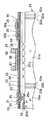
これらの問題について、Al薄膜層/バリアメタル/薄膜抵抗体からなるサンドイッチ構造のパターニング工程を示す図17〜図19を基に具体的に説明する。なお、図17に示すパターニング工程と図18及び図19に示すパターニング工程は異なった工程を採用したものであり、図17はバリアメタルをパターニングしてから薄膜抵抗体をパターニングする場合を示し、図18及び図19はバリアメタルをパターニングする前に薄膜抵抗体をパターニングしておく場合を示している。
【0006】
図17に示す工程を採用する場合、まず図17(a)に示すようにBPSG等からなる絶縁膜101上に薄膜抵抗体を構成するCrSi膜102及びバリアメタルを構成するTiW膜103を順に成膜したのち、図17(b)に示すようにレジスト104をマスクとしてTiW膜103をパターニングしてバリアメタルを形成する。このとき、TiWの残渣103aがCrSi膜102上に残る。このため、図17(c)に示すようにCrSi膜102を例えばケミカルドライエッチング等によりパターニングして薄膜抵抗体の形状を画定する際に、残渣103aが影響してパターニングが良好に行えなくなる。
【0007】
一方、図18及び図19に示す工程を採用する場合、まず、図18(a)に示すように絶縁膜201上に形成された1stAl202の近傍に絶縁膜203を介して薄膜低抗体204を形成したのち、図18(b)に示すようにバリアメタルを構成するTiW膜205及びAl薄膜層206を順に成膜し、図18(c)に示すようにレジスト207をマスクとしてAl薄膜層206をパターニングし、さらに図19(a)に示すようにTiW膜205をパターニングしてバリアメタルを形成する。このとき、TiWの残渣205aが薄膜抵抗体204や絶縁膜203の上に残る。このため、図19(b)に示すように絶縁膜208を介して配線パターン209を形成したときに、残渣205aによって配線パターン209の間をショートさせてしまう。
【0008】
なお、エッチング時間を長くしたり、エッチング液の温度条件を変えても、残渣103a、205aを除去することは容易でなく、逆に例えば、エッチング時間を長くするとパターニングマスクとしてのレジストが剥離してしまい、パターニング精度が悪化してしまうという問題を発生させてしまい好ましくない。
【0009】
本発明は上記問題に鑑みて成され、タングステンを含む電極材料をパターニングする際に発生する残渣による影響をなくし、薄膜抵抗体のパターニングが安定に行え、配線をショートさせない半導体装置の製造方法を提供することを目的とする。
【0010】
【課題を解決するための手段】
上記目的を達成するため、以下の技術的手段を採用する。
【0016】
請求項1に記載の発明においては、タングステンを含むバリアメタル(38)のパターニング時に発生した該バリアメタル(38)の残渣(38a)を酸素プラズマ雰囲気にて酸化したのち、該酸化後の残渣をアルカリ性溶液を用いて溶解することにより除去する工程を備えていることを特徴としている。
【0017】
このように、タングステンを含むバリアメタル(38)のパターニング時に発生したバリアメタル(38)の残渣(38a)を酸素プラズマ雰囲気にて酸化したのち、該酸化後の残渣をアルカリ性溶液を用いて溶解することにより除去することにより、バリアメタル(38)をパターニングする際に除去が困難であった残渣(38a)を完全に除去することができる。これにより、残渣(38a)による影響をなくし、薄膜抵抗体のパターニングが安定に行え、配線をショートさせないようにできる。
【0018】
具体的には、請求項2に示すように、薄膜抵抗体(37)を構成する金属薄膜上にタングステンを含むバリアメタル(38)を形成したのち、バリアメタル(38)をウェットエッチングによってパターニングし、このバリアメタル(38)のパターニングによって発生した該バリアメタル(38)の残渣(38a)を酸素プラズマ雰囲気にて酸化したのち、該酸化後の残渣をアルカリ性溶液を用いて溶解することにより除去することにより、この後行う薄膜抵抗体(37)のパターニングを安定して行うことができる。
【0019】
また、請求項3に示すように、薄膜抵抗体(37)をパターニングしたのち、薄膜抵抗体(37)上にタングステンを含むバリアメタル(38)を形成し、このバリアメタル(38)をウェットエッチングによってパターニングするときに発生した該バリアメタル(38)の残渣(38a)を酸素プラズマ雰囲気にて酸化したのち、該酸化後の残渣をアルカリ性溶液を用いて溶解することにより除去することにより、この後形成される配線パターンが残渣(38a)によってショートしないようにできる。
【0020】
請求項4に記載の発明においては、バリアメタル(38)のパターニングマスクとしてのレジスト(45、51)を該バリアメタル(38)の上に配置する工程を有し、残渣(38a)を除去する工程は、レジスト(45、51)を除去する際に残渣(38a)を同時に除去することを特徴としている。
【0021】
このように、残渣(38a)をレジスト(45、51)と同時に除去することにより、製造工程の簡略化を図ることができる。
【0022】
具体的には、請求項5に示すように、バリアメタル(38)の残渣(38a)を有機系アミンで除去することができる。
【0023】
また、請求項6に示す構成によれば、残渣(38a)を除去したのちに薄膜抵抗体(37)のパターニングを行うようにしているため、薄膜抵抗体(37)のパターニングを安定して行うことができ、請求項7に示す構成によれば、残渣(38a)を除去したのちに絶縁膜(40)を形成しているため、コンタクトホール(40a)内に形成される配線パターンが残渣(38a)によってショートしないようにできる。
【0024】
なお、上記した括弧内の符号は、後述する実施形態記載の具体的手段との対応関係を示すものである。
【0025】
【発明の実施の形態】
以下、本発明を図に示す実施形態について説明する。
【0026】
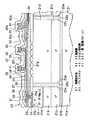
図1は、本発明の一実施形態を適用して製造したMOSFETの集積回路の一断面を示している。
【0027】
シリコン基板21はSOI(silicon on insulator)構造で構成されており、高不純物濃度のp型基板21a上にシリコン酸化膜21bを介して高不純物濃度のn型層21c及び低不純物濃度のn型層21dが積層された構成となっている。
【0028】
このシリコン基板21には、トレンチを埋め込んだシリコン酸化膜22a及び多結晶シリコン層22bが形成されており、これらによって素子(MOSFET)形成領域23と薄膜抵抗体形成領域24とが素子分離されている。
【0029】
素子形成領域23において、n型層21dにはp型不純物が導入されてp型ウェル層23aが形成されている。このp型ウェル層23aの表層部にはn型のソース領域25a及びn型のドレイン領域25bが形成されている。
【0030】
ソース領域25a及びドレイン領域25bとの間におけるp型ウェル層23aの表層部にはゲート酸化膜26が形成されている。なお、シリコン基板21の表面にはLOCOS膜27が形成されており、素子形成領域23と薄膜抵抗体形成領域24とが素子分離されている。
【0031】
ゲート酸化膜26上にはゲート電極28が形成されており、ゲート電極28は絶縁膜としてのBPSG膜29で覆われている。ソース領域25a(およびドレイン領域25b)はコンタクトホールを介してTiN膜30及び1stAl膜としてのAlSiCu膜31(ソース電極やドレイン電極)に接続されている。なお、薄膜抵抗体形成領域24内のBPSG膜29上に形成された配線パターン32a、32bは、1stAl膜としてAlSiCu膜31を形成する際に同時に形成されたものである。
【0032】
ゲート電極28及びソース電極(ドレイン電極)31はP−SiN膜33、TEOS膜34、SOG(spin on glass)35、及びTEOS膜36によって覆われている。
【0033】
そして、シリコン酸化膜36の上の所定位置に薄膜抵抗体37が形成されている。薄膜抵抗体37は、CrSi膜で構成されており、膜厚が15nm程度となっている。LOCOS膜27のうち、薄膜抵抗体37の下方に位置する部分27aは凹凸形状を成しており、レーザートリミングの際にレーザ光が散乱されるようになっている。
【0034】
薄膜抵抗体37の両端には、TiW膜からなるバリアメタル38が備えられており、バリアメタル38の上には薄膜抵抗体用電極としてのAl薄膜層39が備えられている。
【0035】
そして、薄膜抵抗体37を含むシリコン基板21の上面全面を覆うように、層間絶縁膜としてのシリコン酸化膜40が形成されており、このシリコン酸化膜40に形成されたビアホール40aを介して配線パターンを成す2ndAl膜としてのAl薄膜層41が形成されている。さらに、Al薄膜膜41を含むシリコン基板21の上面全面がP−SiN膜からなる保護膜42で覆われている。
【0036】
このように構成されたMOSFETの集積回路は、薄膜抵抗体37の抵抗値を調整するためにレーザートリミング処理される。このとき、上述したように、薄膜抵抗体37の下方のLOCOS膜27が凹凸形状となっているため、レーザ光を散乱させることができる。このため、レーザ光の干渉等を低減することができ、薄膜抵抗体37の溶断が良好に行われる。
【0037】
次に、図1に示したMOSFETの集積回路の製造方法について図2〜図12に基づいて説明する。
【0038】
〔図2に示す工程〕
高不純物濃度のp型基板21a上にシリコン酸化膜21bを介して高不純物濃度のn型層21c及び低不純物濃度のn型層21dが積層されたSOI構造のシリコン基板21を用意する。
【0039】
そして、各素子の境界部分にシリコン酸化膜21bまで達するトレンチを形成したのち、トレンチの側壁にシリコン酸化膜22aを形成すると共に、シリコン酸化膜22aの間を他結晶シリコン層22bで埋めて素子分離を行う。
【0040】
次に、選択的にイオン注入を行い、MOSFET形成領域23におけるn型層21dの表層部にp型ウェル層23aを形成する。そして、LOCOS酸化によりトレンチ上にLOCOS酸化膜27を形成する。このとき、薄膜抵抗体形成領域においては、薄膜抵抗体37(図1参照)のレーザートリミングの加工性を向上させる構造として、LOCOS膜27が凹凸形状となるようにしている。
【0041】
さらに、p型ウェル層23a上にゲート酸化膜26を形成したのち、ポリシリコンを堆積する。そして、ポリシリコンをパターニングしてゲート電極28を形成する。この後、ゲート電極28をマスクとしてイオン注入を行い熱処理を行うことでソース領域25a、ドレイン領域25bを形成する。
【0042】
その後、シリコン基板21の表面全面に層間絶縁膜となるBPSG膜29をCVD法等により形成し、リフロー処理を行う。
【0043】
〔図3に示す工程〕
BPSG膜29にコンタクトホール29aを形成したのち、900〜950℃程度のリフロー処理を施し、コンタクトホール29aのエッジ部がなだらかになるようにする。
【0044】
〔図4に示す工程〕
バリアメタルとしてのTiN膜30を100nm程度の膜厚で形成する。そして、スパッタによりAlSiCu膜を0.45μm程度の膜厚で成膜したのち、1stAl膜31をECR(Electoron cyclotron resonance)ドライエッチングにてパターニングする。
【0045】
〔図5に示す工程〕
まず、P−SiN膜33を0.1μmの厚さで形成したのち、CVD法によりTEOS膜34を0.2μm程度の厚さで形成する。さらに、SOGを塗布したのち、ベーク及びエッチバック処理にてSOG35でシリコン基板21の表面の凹凸部分を埋め、平坦化する。また、CVD法によりTEOS膜36を0.3μm程度の膜厚で成膜する。
【0046】
〔図6に示す工程〕
そして、スパッタによりCrSi膜を15nm程度の膜厚で成膜したのち、CrSi膜をパターニングして薄膜抵抗体37を形成する。
【0047】
さらに、薄膜抵抗体37上を含むシリコン基板21の上面全面にTiW膜からなるバリアメタル38を1000Å程度の膜厚で成膜する。
【0048】
〔図7に示す工程〕
薄膜抵抗体用の電極となるAl膜39を2000Å程度の膜厚で成膜する。そして、フォトリソグラフィ工程を実施するために、フォトレジスト45をパターニングして薄膜抵抗体37の両端に残す。
【0049】
〔図8に示す工程〕
フォトレジスト45をマスクとしてウェットエッチングを行い、Al薄膜層39をパターニングする。
【0050】
〔図9に示す工程〕
フォトレジスト45をマスクとしてウェットエッチングを行いバリアメタル38をパターニングする。このウェットエッチングには、H2O2/NH4OH系溶液をエッチング液として使用しているため、過酸化水素のみの場合に比べて高エッチレートが実現でき、フォトレジスト45が浮いてしまうのを防止できる。
【0051】
このとき、TiWは次の反応により錯イオンとなって溶解するものと考えられる。
【0052】
【化1】
Ti+6NH4++4e-→[Ti(NH3)6]2++3H2
【0053】
【化2】
W+8OH-→[WO4]2-+4H2O+6e-
ここで、WよりTiの反応の方が活性であると考えられ、その結果、上述したように薄膜抵抗体37及びTEOS膜36の上にTiを含まないW膜(10Å程度)がTiWのエッチング残りである残渣38aとして最終的に残るものと推定される。
【0054】
次に、酸素プラズマ処理にて残渣38aを充分に酸化し、酸化物を形成する。この酸素プラズマ処理によると、残渣38aの酸化時にフォトレジスト45が焦げつくことはない。
【0055】
〔図10に示す工程〕
そして、フォトレジスト45と共に酸化させた残渣38aを有機系アミン等のレジスト剥離液で除去する。このとき、酸化させた残渣38aは、レジスト剥離液に溶解し、フォトレジスト45と共に完全に除去される。
【0056】
すなわち、タングステン残渣38aが酸化されることにより、OH-基との親和性ができ、次の化学式に示すようにアルカリ性溶液に溶解しやすくなり、除去できるようになるのである。
【0057】
【化3】
WO3+2OH−→[WO4]2-+H2O
〔図11に示す工程〕
シリコン基板21の表面全面をシリコン酸化膜(SiO2)40で覆う。
【0058】
〔図12に示す工程〕
シリコン酸化膜40にビアホール40aを形成したのち、このビアホール40aを介して2ndAl膜としてのAlSi膜(配線パターン)41をパターニングする。
【0059】
このとき、上述したようにバリアメタル38を除去したときに発生する残渣38aを完全に除去しているため、残渣38aの影響によってAlSi膜41同士がショートすることはない。
【0060】
さらに、AlSi膜41を含むシリコン基板21の上面全面をP−SiN膜からなる保護膜42で覆ったのち、リフロー処理を施す。これにより、図1に示したMOSFETの集積回路が完成する。
【0061】
このように、タングステンを含むバリアメタル(TiW)38をウェットエッチングしたときに発生する残渣38aを酸化してタングステン酸化物を生成し、アルカリ性溶液で除去するようにしている。従って、ウェットエッチングのみでは除去が困難であった残渣38aを完全に除去することができ、残渣38aによる配線パターンのショートを防止することができる。
【0062】
(第2実施形態)
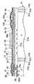
本実施形態では、第1実施形態とバリアメタル38のパターニング方法が異なる場合を示す。図13〜図16に本実施形態におけるMOSFETの集積回路の製造工程を示す。なお、これらの図は、第1実施形態で説明した製造工程と異なる部分のみを示したものであるため、同様の工程の部分は第1実施形態を参照して説明する。
【0063】
まず、図2〜図5に示す工程を施す。そして、図13〜図16に示す工程を施す。
【0064】
〔図13に示す工程〕
まず、スパッタによりCrSi膜37を15nm程度の膜厚で成膜したのち、さらにこのCrSi膜からなる薄膜抵抗体37上にTiWからなるバリアメタル38を1000Å程度の膜厚で成膜する。
【0065】
そして、フォトレジスト51を堆積して、所望の領域にのみフォトレジスト51を残す。
【0066】
そして、バリアメタル38をパターニングする。このとき、薄膜抵抗体37の上にTiWの残渣38aが残る。
【0067】
その後、酸化プラズマ処理によって残渣38aを酸化させる。
【0068】
〔図14に示す工程〕
そして、フォトレジスト51と共に酸化させた残渣38aを有機系アミン等のレジスト剥離液で除去する。このとき、酸化させた残渣38aは、レジスト剥離液に溶解し、フォトレジスト51と共に完全に除去される。
【0069】
この後、薄膜抵抗体37をCF4及び酸素を用いたケミカルドライエッチングによりパターニングする。このとき、バリアメタル38をパターニングしたときに形成される残渣38aが完全に除去された状態になっているため、薄膜抵抗体37のパターニングを安定して行うことができる。
【0070】
〔図15に示す工程〕
次に、薄膜抵抗体用の電極となるAl薄膜層39を2000Å程度の膜厚で成膜する。そして、フォトリソグラフィ工程を実施するために、フォトレジスト55をパターニングし、薄膜抵抗体37の両端にフォトレジスト55を残す。
【0071】
この後、フォトレジスト55をマスクとしてドライエッチングを行い、Al薄膜層39をパターニングする。
【0072】
〔図16に示す工程〕
そして、フォトレジスト55をマスクとしてウェットエッチングを行い、バリアメタル38をパターニングする。このウェットエッチングには、H2O2/NH4OH系溶液をエッチング液として使用している。また、この際にも、CrSi膜からなる薄膜抵抗体37上にTiWの残渣が残る。従って、上述と同様に酸化プラズマ処理、アルカリ性溶液による処理により残渣を除去する。
【0073】
この後、図11〜図12に示す工程を経てMOSFETの集積回路が完成する。
【0074】
このように、バリアメタル38のパターニングの際に発生する残渣38aを除去することにより、薄膜抵抗体37のパターニングが安定に行えるようにすることができる。
【0075】
(他の実施形態)
なお、上記第1、第2実施形態では残渣38aをフォトレジスト45、51と共に除去するようにしているが、これはフォトレジスト45、51を剥離するにに使用する有機系アミン溶液によって酸化した残渣38aが溶解するためであり、必ずしも酸化した残渣38aをフォトレジスト45、51と同時に除去しなければならないわけではなく、他のアルカリ性溶液、例えば残渣酸化後に再度H2O2/NH4OH系溶液により除去してもよい。但し、上述のようにフォトレジスト45、51と同時に酸化した残渣38aを除去することにより、製造工程の簡略化を図ることができる。また、タングステン残渣を酸化する方法も、O2プラズマ処理に限らず、ベーキングやオゾンプラズマ処理など、他の酸化処理が利用可能である。
【0076】
また、上記第1、第2実施形態では、薄膜抵抗体37の電極部のバリアメタル38としてのチタンタングステンのパターニングに本発明を適用した例を示したが、チタンタングステン合金以外にも適用できる。例えば、タングステン膜、シリコンを含有したタングステンであるタングステンシリサイド膜、モリブデンタングステン膜、タンタルタングステン膜など、タングステンを含む材料のエッチング等に対して適用可能である。
【0077】
タングステンあるいはその合金は各種半導体装置の配線などにも広く用いられており、これらのエッチング時にも応用することができる。例えば、タングステンやタングステンシリサイドはMOSFET素子やTFT素子のゲート電極に、単独あるいはポリシリコンとの積層構造(ポリサイド構造あるいはポリメタル構造)で用いられている。また、特にタングステンは最近ではサブミクロンレベルの微細なコンタクトホールやビアホールの埋め込み金属としても、広く用いられるようになっている。さらに、コンタクトホールやビアホールを埋め込んだ後、基板全面に成膜されたタングステンを直接加工して配線として用いる場合もある。また、上述のチタンタングステンは、バリアメタルとして薄膜抵抗体のみならず半導体素子の電極部に用いられることも、アルミニウムや金等と積層構造にして配線として用いられることもある。
【0078】
上述の第1、第2実施形態では下層側の薄膜抵抗体37への影響を考え、バリアメタル38としてのチタンタングステンの加工はウェットエッチングにて行うようにしていたが、そのような制約のない構造におけるタングステンやタングステン合金の加工はドライエッチングで行なうのが一般的である。例えばタングステンはSF6/N2やCF4/O2等のガスで、タングステンシリサイドはSF6/Cl2やSF6/HBr 等のガスで、チタンタングステンはCF4/O2やSF6/Ar 等のガスでエッチングされる。
【0079】
しかしながら、例えばチタンタングステンをドライエッチングで加工する場合、ドライエッチング装置のエッチング室や排気配管内にチタンが付着しやすく、パーティクル発生の原因になるという問題もあり、処理能力に優るウェットエッチングで加工することが望まれている。その場合、下地のシリコンやシリコン酸化膜、シリコン窒化膜、ガラス等に対してエッチング選択性がとれるように、上述と同様、過酸化水素水や過酸化水素とアンモニアと水の混合液でパターニングすることになるが、この場合もエッチング後に粒状または被膜状のエッチング残渣が発生し、これが原因となって電極間、配線間のリーク、あるいはポリサイド、ポリメタル構造のゲート、配線では下地のポリシリコンの加工精度の悪化を引き起こしてしまうことが懸念される。
【0080】
従って、これらデバイス構造においても上述した本願発明の残渣除去技術を応用して、すなわち発生したタングステン残渣を酸化してタングステン酸化物に一旦変換し、アルカリ性溶液にて溶解除去するようにすれば、こうした残渣に起因した問題は効果的に防止できる。
【0081】
また、本発明は残渣除去技術のみならず、タングステンを含む配線材料をパターニングする際のパターニング技術に応用することも可能である。例えば、薄膜のタングステンを電極材料として堆積した後、その配線として不要な部分を選択的に酸化してアルカリ性溶液にて除去するようにすればよい。
【図面の簡単な説明】
【図1】本発明の一実施形態を適用して形成したMOSFET部とCrSi抵抗部との集積回路を示す図である。
【図2】図1に示す集積回路の製造工程を示す図である。
【図3】図2に続く集積回路の製造工程を示す図である。
【図4】図3に続く集積回路の製造工程を示す図である。
【図5】図4に続く集積回路の製造工程を示す図である。
【図6】図5に続く集積回路の製造工程を示す図である。
【図7】図6に続く集積回路の製造工程を示す図である。
【図8】図7に続く集積回路の製造工程を示す図である。
【図9】図8に続く集積回路の製造工程を示す図である。
【図10】図9に続く集積回路の製造工程を示す図である。
【図11】図10に続く集積回路の製造工程を示す図である。
【図12】図11に続く集積回路の製造工程を示す図である。
【図13】第2実施形態によるMOSFET部とCrSi抵抗部との集積回路の製造工程を示す図である。
【図14】図13に続く集積回路の製造工程を示す図である。
【図15】図14に続く集積回路の製造工程を示す図である。
【図16】図15に続く集積回路の製造工程を示す図である。
【図17】従来におけるバリアメタルをパターニングしたときの様子を説明するための図である。
【図18】従来におけるバリアメタルをパターニングしたときの様子を説明するための図である。
【図19】従来におけるバリアメタルをパターニングしたときの様子を説明するための図である。
【符号の説明】
21…シリコン基板、36…シリコン酸化膜、37…薄膜抵抗体、
38…バリアメタル、38a…残渣、39…Al薄膜層、
40…シリコン酸化膜、41…AlSi膜、42…保護膜。[0001]
BACKGROUND OF THE INVENTION
The present invention relates to an etching method and a method of manufacturing a semiconductor device having a thin film resistor using this etching method, and is particularly suitable for application to etching for forming wiring, barrier metal, etc. by tungsten or its alloy. .
[0002]
[Prior art]
For example, in the electrode structure of a thin film resistor made of CrSi or the like, a barrier metal is sandwiched between the thin film resistor and the Al thin film layer in order to avoid characteristic deterioration due to mutual diffusion between the thin film resistor and the Al thin film layer. The structure of Al thin film layer / barrier metal / thin film resistor is adopted.
[0003]
When patterning the barrier metal, if the barrier metal is processed by dry etching, the etching selectivity between the barrier metal and the thin film resistor cannot be taken sufficiently by the dry etching, so that even the thin film resistor exposed during overetching is etched. . In general, since a thin film resistor is as thin as about 10 nm, etching of the thin film resistor has a great influence on characteristics such as a resistance value. For this reason, it is necessary to pattern the barrier metal by wet etching with a sufficient etching selectivity.
[0004]
[Problems to be solved by the invention]
However, a residue is generated during the wet etching of the barrier metal, and this residue has a problem in that the thin film resistor cannot be satisfactorily patterned or the wiring is short-circuited.
[0005]
These problems will be specifically described with reference to FIGS. 17 to 19 showing a patterning process of a sandwich structure composed of an Al thin film layer / barrier metal / thin film resistor. The patterning process shown in FIG. 17 and the patterning process shown in FIGS. 18 and 19 employ different processes. FIG. 17 shows a case where the thin film resistor is patterned after the barrier metal is patterned. 18 and 19 show the case where the thin film resistor is patterned before the barrier metal is patterned.
[0006]
When the process shown in FIG. 17 is adopted, first, as shown in FIG. 17A, a CrSi
[0007]
On the other hand, when the steps shown in FIGS. 18 and 19 are adopted, first, as shown in FIG. 18A, a thin
[0008]
Even if the etching time is increased or the temperature conditions of the etching solution are changed, it is not easy to remove the
[0009]
The present invention has been made in view of the above problems, and provides a method of manufacturing a semiconductor device that eliminates the influence of residues generated when patterning an electrode material containing tungsten, can stably pattern a thin film resistor, and does not short-circuit a wiring. The purpose is to do.
[0010]
[Means for Solving the Problems]
In order to achieve the above object, the following technical means are adopted.
[0016]
In the first aspect of the present invention, after the barrier metal (38) residue (38a) generated during the patterning of thetungsten-containing barrier metal (38) is oxidized in an oxygen plasma atmosphere, the oxidized residue is removed. It is characterized by having a step of removing by dissolving using an alkaline solution.
[0017]
Thus, after oxidizing the residue (38a) of the barrier metal (38) generated during the patterning of the barrier metal (38)containing tungsten in an oxygen plasma atmosphere, the oxidized residue is dissolved using an alkaline solution. Thus, the residue (38a) that was difficult to remove when patterning the barrier metal (38) can be completely removed. As a result, the influence of the residue (38a) can be eliminated, the thin film resistor can be stably patterned, and the wiring can be prevented from being short-circuited.
[0018]
Specifically, as shown in
[0019]
According to another aspect of the present invention, after the thin film resistor (37) is patterned, a barrier metal (38)containing tungsten is formed on the thin film resistor (37), and the barrier metal (38) is wet-etched. After oxidizing the residue (38a) of the barrier metal (38) generated when patterning by an oxygen plasma atmosphere, the oxidized residue is removed by dissolution using an alkaline solution. The formed wiring pattern can be prevented from being short-circuited by the residue (38a).
[0020]
According to afourth aspect of the present invention, the method includes the step of disposing a resist (45, 51) as a patterning mask for the barrier metal (38) on the barrier metal (38), and removing the residue (38a). The process is characterized in that the residue (38a) is simultaneously removed when removing the resist (45, 51).
[0021]
Thus, by removing the residue (38a) simultaneously with the resist (45, 51), the manufacturing process can be simplified.
[0022]
Specifically, as shown in claim5 , the residue (38a) of the barrier metal (38) can be removed with an organic amine.
[0023]
Further, according to the configuration of thesixth aspect , since the thin film resistor (37) is patterned after the residue (38a) is removed, the thin film resistor (37) is stably patterned. According to the structure shown in claim7 , since the insulating film (40) is formed after the residue (38a) is removed, the wiring pattern formed in the contact hole (40a) becomes a residue ( 38a) can prevent short-circuiting.
[0024]
In addition, the code | symbol in the above-mentioned parenthesis shows the correspondence with the specific means of embodiment description later mentioned.
[0025]
DETAILED DESCRIPTION OF THE INVENTION
DESCRIPTION OF THE PREFERRED EMBODIMENTS Embodiments shown in the drawings will be described below.
[0026]
FIG. 1 shows a cross section of a MOSFET integrated circuit manufactured by applying one embodiment of the present invention.
[0027]
The
[0028]
The
[0029]
In the
[0030]
A
[0031]
A
[0032]
The
[0033]
A
[0034]
A
[0035]
A
[0036]
The MOSFET integrated circuit configured as described above is subjected to laser trimming to adjust the resistance value of the
[0037]
Next, a method for manufacturing the MOSFET integrated circuit shown in FIG. 1 will be described with reference to FIGS.
[0038]
[Steps shown in FIG. 2]
An SOI
[0039]
Then, after forming a trench reaching the
[0040]
Next, ion implantation is selectively performed to form a p-
[0041]
Further, after forming a
[0042]
Thereafter, a
[0043]
[Steps shown in FIG. 3]
After the
[0044]
[Steps shown in FIG. 4]
A
[0045]
[Steps shown in FIG. 5]
First, after forming the P-
[0046]
[Steps shown in FIG. 6]
Then, after forming a CrSi film with a thickness of about 15 nm by sputtering, the
[0047]
Further, a
[0048]
[Steps shown in FIG. 7]
An
[0049]
[Steps shown in FIG. 8]
Wet etching is performed using the
[0050]
[Steps shown in FIG. 9]
The
[0051]
At this time, TiW is considered to be dissolved as complex ions by the following reaction.
[0052]
[Chemical 1]
Ti + 6NH4+ + 4e− → [Ti (NH3 )6 ]2+ + 3H2
[0053]
[Chemical 2]
W + 8OH− → [WO4 ]2− + 4H2 O + 6e−
Here, it is considered that the reaction of Ti is more active than W. As a result, as described above, the W film not containing Ti (about 10 mm) on the
[0054]
Next, the
[0055]
[Steps shown in FIG. 10]
Then, the
[0056]
That is, when the
[0057]
[Chemical 3]
WO3 + 2OH− → [WO4 ]2- + H2 O
[Steps shown in FIG. 11]
The entire surface of the
[0058]
[Steps shown in FIG. 12]
After forming a via
[0059]
At this time, since the
[0060]
Further, the entire upper surface of the
[0061]
In this way, the
[0062]
(Second Embodiment)
In this embodiment, the case where the patterning method of the
[0063]
First, the steps shown in FIGS. Then, the steps shown in FIGS. 13 to 16 are performed.
[0064]
[Steps shown in FIG. 13]
First, after the
[0065]
Then, a
[0066]
Then, the
[0067]
Thereafter, the
[0068]
[Steps shown in FIG. 14]
Then, the
[0069]
Thereafter, the
[0070]
[Steps shown in FIG. 15]
Next, an Al
[0071]
Thereafter, dry etching is performed using the
[0072]
[Steps shown in FIG. 16]
Then, wet etching is performed using the
[0073]
Thereafter, the integrated circuit of the MOSFET is completed through the steps shown in FIGS.
[0074]
Thus, by removing the
[0075]
(Other embodiments)
In the first and second embodiments, the
[0076]
In the first and second embodiments, the example in which the present invention is applied to the patterning of titanium tungsten as the
[0077]
Tungsten or its alloys are widely used for wiring of various semiconductor devices, and can be applied to these etchings. For example, tungsten or tungsten silicide is used for a gate electrode of a MOSFET element or a TFT element alone or in a laminated structure (polycide structure or polymetal structure) with polysilicon. In particular, tungsten has recently been widely used as a buried metal for fine contact holes and via holes on the submicron level. Further, after filling contact holes and via holes, tungsten deposited on the entire surface of the substrate may be directly processed and used as wiring. Further, the above-described titanium tungsten may be used not only as a thin film resistor as a barrier metal but also as an electrode part of a semiconductor element, or may be used as a wiring in a laminated structure with aluminum or gold.
[0078]
In the first and second embodiments described above, considering the influence on the
[0079]
However, when titanium tungsten is processed by dry etching, for example, there is a problem that titanium easily adheres to the etching chamber or exhaust pipe of the dry etching apparatus, which causes generation of particles. It is hoped that. In that case, patterning is performed with hydrogen peroxide solution or a mixed solution of hydrogen peroxide, ammonia and water in the same manner as described above so that etching selectivity can be obtained with respect to the underlying silicon, silicon oxide film, silicon nitride film, glass or the like. However, in this case as well, a granular or film-like etching residue is generated after etching, which causes leakage between electrodes and wiring, or processing of the underlying polysilicon for polycide and polymetal gates and wiring. There is a concern that it may cause deterioration of accuracy.
[0080]
Therefore, even in these device structures, if the residue removal technology of the present invention described above is applied, that is, if the generated tungsten residue is oxidized and converted into tungsten oxide once and dissolved and removed in an alkaline solution, such a device structure is used. Problems caused by the residue can be effectively prevented.
[0081]
Further, the present invention can be applied not only to a residue removal technique but also to a patterning technique for patterning a wiring material containing tungsten. For example, after depositing a thin film of tungsten as an electrode material, an unnecessary portion of the wiring may be selectively oxidized and removed with an alkaline solution.
[Brief description of the drawings]
FIG. 1 is a diagram showing an integrated circuit of a MOSFET portion and a CrSi resistance portion formed by applying one embodiment of the present invention.
2 is a diagram showing a manufacturing process of the integrated circuit shown in FIG. 1; FIG.
3 is a diagram showing manufacturing steps of the integrated circuit following FIG. 2. FIG.
4 is a diagram showing manufacturing steps of the integrated circuit following FIG. 3. FIG.
5 is a diagram showing manufacturing steps of the integrated circuit following FIG. 4. FIG.
6 is a diagram showing manufacturing steps of the integrated circuit following FIG. 5. FIG.
7 is a diagram showing manufacturing steps of the integrated circuit following FIG. 6. FIG.
8 is a diagram showing manufacturing steps of the integrated circuit following FIG. 7. FIG.
9 is a diagram showing manufacturing steps of the integrated circuit following FIG. 8. FIG.
10 is a diagram showing manufacturing steps of the integrated circuit following FIG. 9. FIG.
11 is a diagram showing manufacturing steps of the integrated circuit following FIG. 10. FIG.
12 is a diagram showing manufacturing steps of the integrated circuit following FIG. 11. FIG.
FIG. 13 is a diagram showing manufacturing steps of the integrated circuit of the MOSFET portion and the CrSi resistance portion according to the second embodiment.
14 is a diagram showing manufacturing steps of the integrated circuit following FIG. 13. FIG.
15 is a diagram showing manufacturing steps of the integrated circuit following FIG. 14. FIG.
FIG. 16 is a diagram illustrating the manufacturing process for the integrated circuit, following FIG. 15;
FIG. 17 is a diagram for explaining a state in which a conventional barrier metal is patterned.
FIG. 18 is a diagram for explaining a state in which a conventional barrier metal is patterned.
FIG. 19 is a diagram for explaining a state in which a conventional barrier metal is patterned.
[Explanation of symbols]
21 ... Silicon substrate, 36 ... Silicon oxide film, 37 ... Thin film resistor,
38 ... Barrier metal, 38a ... Residue, 39 ... Al thin film layer,
40 ... silicon oxide film, 41 ... AlSi film, 42 ... protective film.
Claims (7)
Translated fromJapanese前記バリアメタル(38)のパターニング時に発生した該バリアメタルの残渣(38a)を酸素プラズマ雰囲気にて酸化したのち、該酸化後の残渣をアルカリ性溶液を用いて溶解することにより除去する工程を備えていることを特徴とする半導体装置の製造方法。A thin film resistor (37),a barrier metal (38)containing tungsten, and an electrode material (39) are sequentially disposed on the substrate (21), and the barrier metal (38) is wet based on the patterned electrode material (39). In the method of manufacturing a semiconductor device in which the thin film resistor (37) is determined by patterning by etching, and a barrier metal is arranged at an electrode extraction position of the thin film resistor (37).
A step of oxidizing the barrier metal residue (38a) generated during the patterning of the barrier metal (38) in an oxygen plasma atmosphere and then removing the oxidized residue by dissolving with an alkaline solution. A method for manufacturing a semiconductor device, comprising:
前記半導体基板(21)上の所定領域に、前記絶縁膜(34、36)を介して前記薄膜抵抗体(37)を構成する金属薄膜を形成すると共に、該金属薄膜上にタングステンを含むバリアメタル(38)を形成する工程と、前記バリアメタル(38)をウェットエッチングによってパターニングする工程と、前記バリアメタル(38)のパターニングによって発生した該バリアメタル(38)の残渣(38a)を酸素プラズマ雰囲気にて酸化したのち、該酸化後の残渣をアルカリ性溶液を用いて溶解することにより除去する工程と、前記金属薄膜をパターニングして前記薄膜抵抗体(37)の形状を画定する工程と、を備えていることを特徴とする半導体装置の製造方法。In a method for manufacturing a semiconductor device comprising a thin film resistor (37) formed via an insulating film (34, 36) on a semiconductor substrate (21) on which a semiconductor element is formed,
A metal thin film constituting the thin film resistor (37) is formed in a predetermined region on the semiconductor substrate (21) via the insulating films (34, 36), anda barrier metalcontaining tungsten on the metal thin film. (38), a step of patterning the barrier metal (38) by wet etching, and a residue (38a) of the barrier metal (38) generated by the patterning of the barrier metal (38) And then removing the oxidized residue by dissolving with an alkaline solution and patterning the metal thin film to define the shape of the thin film resistor (37). A method for manufacturing a semiconductor device.
前記半導体基板(21)上の所定領域に、前記絶縁膜(34、36)を介して前記薄膜抵抗体(37)をパターニングする工程と、
前記薄膜抵抗体(37)上にタングステンを含むバリアメタル(38)を形成する工程と、
前記バリアメタル(38)をウェットエッチングによってパターニングする工程と、
前記バリアメタル(38)のパターニングによって発生した該バリアメタル(38)の残渣(38a)を酸素プラズマ雰囲気にて酸化したのち、該酸化後の残渣をアルカリ性溶液を用いて溶解することにより除去する工程と、を備えていることを特徴とする半導体装置の製造方法。In a method for manufacturing a semiconductor device comprising a thin film resistor (37) formed via an insulating film (34, 36) on a semiconductor substrate (21) on which a semiconductor element is formed,
Patterning the thin film resistor (37) in a predetermined region on the semiconductor substrate (21) via the insulating films (34, 36);
Forming a barrier metal (38)containing tungsten on the thin film resistor (37);
Patterning the barrier metal (38) by wet etching;
A step of oxidizing the residue (38a) of the barrier metal (38) generated by the patterning of the barrier metal (38) in an oxygen plasma atmosphere and then removing the oxidized residue by dissolving with an alkaline solution. And a method of manufacturing a semiconductor device.
前記残渣(38a)を除去する工程は、前記レジスト(45、51)を除去する際に同時に前記残渣を除去することを特徴とする請求項2または3に記載の半導体装置の製造方法。Placing a resist (45, 51) as a patterning mask for the barrier metal (38) on the barrier metal (38);
4. The method of manufacturing a semiconductor device according to claim2 , wherein the step of removing the residue (38a) removes the residue simultaneously with the removal of the resist (45, 51).
前記半導体基板(21)上に、前記絶縁膜(34、36)を介して前記薄膜抵抗体(37)を構成する金属薄膜を形成する工程と、
前記薄膜抵抗体(37)上にタングステンを含むバリアメタル(38)を形成する工程と、
前記バリアメタル(38)上の所定領域にレジスト(45)を堆積したのち、該レジスト(45)をマスクとして前記バリアメタル(38)をパターニングする工程と、
前記バリアメタル(38)のパターニングによって発生した該バリアメタル(38)の残渣(38a)を酸素プラズマ雰囲気にて酸化したのち、該酸化後の残渣をアルカリ性溶液を用いて溶解することにより前記レジスト(45)と共に除去する工程と、
前記金属薄膜をパターニングして前記薄膜抵抗体(37)を形成する工程と、
前記バリアメタル(38)の上に導電性薄膜(39)を堆積し、パターニングする工程と、前記導電性薄膜(39)及び前記薄膜抵抗体(37)の上を含む前記半導体基板(21)上に絶縁膜(40)を形成する工程と、
前記絶縁膜に前記導電性薄膜(39)に通ずるコンタクトホール(40a)を形成する工程と、
前記コンタクトホール(40a)を介して前記導電性薄膜(39)に接続される配線パターンを形成する工程と、を備えていることを特徴とする半導体装置の製造方法。In a method for manufacturing a semiconductor device comprising a thin film resistor (37) formed via an insulating film (34, 36) on a semiconductor substrate (21) on which a semiconductor element is formed,
Forming a metal thin film constituting the thin film resistor (37) on the semiconductor substrate (21) via the insulating films (34, 36);
Forming a barrier metal (38)containing tungsten on the thin film resistor (37);
Depositing a resist (45) in a predetermined region on the barrier metal (38) and then patterning the barrier metal (38) using the resist (45) as a mask;
The residue (38a) of the barrier metal (38) generated by the patterning of the barrier metal (38) is oxidized in an oxygen plasma atmosphere, and the oxidized residue is dissolved in an alkaline solution to dissolve the resist ( 45) and removing with
Patterning the metal thin film to form the thin film resistor (37);
On the semiconductor substrate (21) including a step of depositing and patterning a conductive thin film (39) on the barrier metal (38), and on the conductive thin film (39) and the thin film resistor (37). Forming an insulating film (40) on the substrate;
Forming a contact hole (40a) communicating with the conductive thin film (39) in the insulating film;
And a step of forming a wiring pattern connected to the conductive thin film (39) through the contact hole (40a).
前記半導体基板(21)上の所定領域に、前記絶縁膜(34、36)を介して金属薄膜を形成したのち、該金属薄膜をパターニングして前記薄膜抵抗体(37)を形成する工程と、
前記薄膜抵抗体(37)上にタングステンを含むバリアメタル(38)を形成する工程と、
前記バリアメタル(38)の上に導電性薄膜(39)を形成する工程と、
前記導電性薄膜(39)上の所定領域にフォトレジスト(51)を堆積したのち、該フォトレジスト(51)をマスクとして前記導電性薄膜(39)をパターニングする工程と、
前記フォトレジスト(51)をマスクとしたウェットエッチングにより、前記バリアメタル(38)をパターニングする工程と、
前記バリアメタル(38)のパターニングによって発生した該バリアメタル(38)の残渣(38a)を酸素プラズマ雰囲気にて酸化したのち、該酸化後の残渣をアルカリ性溶液を用いて溶解することにより除去する工程と、
前記フォトレジスト(51)を除去する工程と、
前記導電性薄膜(39)及び前記薄膜抵抗体(37)の上を含む前記半導体基板(21)上に絶縁膜(40)を形成する工程と、
前記絶縁膜に前記導電性薄膜(39)に通ずるコンタクトホール(40a)を形成する工程と、
前記コンタクトホール(40a)を介して前記導電性薄膜(39)に接続される配線パターンを形成する工程と、を備えていることを特徴とする半導体装置の製造方法。In a method for manufacturing a semiconductor device comprising a thin film resistor (37) formed via an insulating film (34, 36) on a semiconductor substrate (21) on which a semiconductor element is formed,
Forming a metal thin film in a predetermined region on the semiconductor substrate (21) via the insulating films (34, 36) and then patterning the metal thin film to form the thin film resistor (37);
Forming a barrier metal (38)containing tungsten on the thin film resistor (37);
Forming a conductive thin film (39) on the barrier metal (38);
Depositing a photoresist (51) in a predetermined region on the conductive thin film (39), and then patterning the conductive thin film (39) using the photoresist (51) as a mask;
Patterning the barrier metal (38) by wet etching using the photoresist (51) as a mask;
A step of oxidizing the residue (38a) of the barrier metal (38) generated by the patterning of the barrier metal (38) in an oxygen plasma atmosphere and then removing the oxidized residue by dissolving with an alkaline solution. When,
Removing the photoresist (51);
Forming an insulating film (40) on the semiconductor substrate (21) including the conductive thin film (39) and the thin film resistor (37);
Forming a contact hole (40a) communicating with the conductive thin film (39) in the insulating film;
And a step of forming a wiring pattern connected to the conductive thin film (39) through the contact hole (40a).
Priority Applications (3)
| Application Number | Priority Date | Filing Date | Title |
|---|---|---|---|
| JP20356199AJP4075228B2 (en) | 1998-09-09 | 1999-07-16 | Manufacturing method of semiconductor device |
| US09/390,679US6279585B1 (en) | 1998-09-09 | 1999-09-07 | Etching method and method for manufacturing semiconductor device using the same |
| DE19943175ADE19943175B4 (en) | 1998-09-09 | 1999-09-09 | An etching method and method for producing a semiconductor device using the etching method |
Applications Claiming Priority (3)
| Application Number | Priority Date | Filing Date | Title |
|---|---|---|---|
| JP10-255631 | 1998-09-09 | ||
| JP25563198 | 1998-09-09 | ||
| JP20356199AJP4075228B2 (en) | 1998-09-09 | 1999-07-16 | Manufacturing method of semiconductor device |
Publications (2)
| Publication Number | Publication Date |
|---|---|
| JP2000150459A JP2000150459A (en) | 2000-05-30 |
| JP4075228B2true JP4075228B2 (en) | 2008-04-16 |
Family
ID=26513983
Family Applications (1)
| Application Number | Title | Priority Date | Filing Date |
|---|---|---|---|
| JP20356199AExpired - Fee RelatedJP4075228B2 (en) | 1998-09-09 | 1999-07-16 | Manufacturing method of semiconductor device |
Country Status (3)
| Country | Link |
|---|---|
| US (1) | US6279585B1 (en) |
| JP (1) | JP4075228B2 (en) |
| DE (1) | DE19943175B4 (en) |
Families Citing this family (18)
| Publication number | Priority date | Publication date | Assignee | Title |
|---|---|---|---|---|
| US6277738B1 (en)* | 1999-06-23 | 2001-08-21 | Hyundai Electronics Industries Co., Ltd. | Method of manufacturing a semiconductor device capable of reducing contact resistance |
| JP2001015479A (en)* | 1999-06-29 | 2001-01-19 | Toshiba Corp | Method for manufacturing semiconductor device |
| DE10014915B4 (en)* | 2000-03-17 | 2007-08-16 | Infineon Technologies Ag | Method for exposing a contact surface |
| JP3627617B2 (en) | 2000-04-06 | 2005-03-09 | 株式会社デンソー | Method for processing refractory metal and method for manufacturing semiconductor device using this metal |
| US7514283B2 (en) | 2003-03-20 | 2009-04-07 | Robert Bosch Gmbh | Method of fabricating electromechanical device having a controlled atmosphere |
| US6936491B2 (en) | 2003-06-04 | 2005-08-30 | Robert Bosch Gmbh | Method of fabricating microelectromechanical systems and devices having trench isolated contacts |
| US7075160B2 (en) | 2003-06-04 | 2006-07-11 | Robert Bosch Gmbh | Microelectromechanical systems and devices having thin film encapsulated mechanical structures |
| US6952041B2 (en) | 2003-07-25 | 2005-10-04 | Robert Bosch Gmbh | Anchors for microelectromechanical systems having an SOI substrate, and method of fabricating same |
| US7068125B2 (en) | 2004-03-04 | 2006-06-27 | Robert Bosch Gmbh | Temperature controlled MEMS resonator and method for controlling resonator frequency |
| US7102467B2 (en) | 2004-04-28 | 2006-09-05 | Robert Bosch Gmbh | Method for adjusting the frequency of a MEMS resonator |
| US7410879B1 (en) | 2005-07-11 | 2008-08-12 | National Semiconductor Corporation | System and method for providing a dual via architecture for thin film resistors |
| US7332403B1 (en)* | 2005-07-11 | 2008-02-19 | National Semiconductor Corporation | System and method for providing a buried thin film resistor having end caps defined by a dielectric mask |
| US20070085654A1 (en)* | 2005-10-14 | 2007-04-19 | Georgia Tech Research Corporation | Process development and optimization of embedded thin film resistor on body |
| US20070170528A1 (en) | 2006-01-20 | 2007-07-26 | Aaron Partridge | Wafer encapsulated microelectromechanical structure and method of manufacturing same |
| US7829428B1 (en) | 2008-08-26 | 2010-11-09 | National Semiconductor Corporation | Method for eliminating a mask layer during thin film resistor manufacturing |
| JP2012248814A (en)* | 2011-05-31 | 2012-12-13 | Toshiba Corp | Semiconductor device and manufacturing method of the same |
| KR102426051B1 (en) | 2016-05-31 | 2022-07-26 | 삼성전자주식회사 | Semiconductor device and fabrication method thereof |
| US10541214B2 (en) | 2018-04-27 | 2020-01-21 | Juniper Networks, Inc. | Enhanced bonding between III-V material and oxide material |
Family Cites Families (14)
| Publication number | Priority date | Publication date | Assignee | Title |
|---|---|---|---|---|
| US4443295A (en)* | 1983-06-13 | 1984-04-17 | Fairchild Camera & Instrument Corp. | Method of etching refractory metal film on semiconductor structures utilizing triethylamine and H2 O2 |
| JPS60163466A (en)* | 1984-02-06 | 1985-08-26 | Hitachi Ltd | Manufacturing method of semiconductor device |
| US4878770A (en) | 1987-09-09 | 1989-11-07 | Analog Devices, Inc. | IC chips with self-aligned thin film resistors |
| JP2762473B2 (en) | 1988-08-24 | 1998-06-04 | 株式会社デンソー | Method for manufacturing semiconductor device |
| US5279771A (en)* | 1990-11-05 | 1994-01-18 | Ekc Technology, Inc. | Stripping compositions comprising hydroxylamine and alkanolamine |
| JP3026656B2 (en) | 1991-09-30 | 2000-03-27 | 株式会社デンソー | Manufacturing method of thin film resistor |
| US5382916A (en) | 1991-10-30 | 1995-01-17 | Harris Corporation | Differential voltage follower |
| EP0620586B1 (en) | 1993-04-05 | 2001-06-20 | Denso Corporation | Semiconductor device having thin film resistor |
| JPH07202124A (en) | 1993-12-28 | 1995-08-04 | Fujitsu Ltd | Method for manufacturing semiconductor device |
| US5420063A (en) | 1994-04-11 | 1995-05-30 | National Semiconductor Corporation | Method of producing a resistor in an integrated circuit |
| JP2932940B2 (en)* | 1994-06-08 | 1999-08-09 | 株式会社デンソー | Method of manufacturing semiconductor device having thin film resistor |
| JP2701773B2 (en) | 1995-03-15 | 1998-01-21 | 日本電気株式会社 | Etching method |
| JP3206435B2 (en) | 1996-07-02 | 2001-09-10 | 株式会社デンソー | Semiconductor device and method of manufacturing the same |
| JP3374680B2 (en)* | 1996-11-06 | 2003-02-10 | 株式会社デンソー | Method for manufacturing semiconductor device |
- 1999
- 1999-07-16JPJP20356199Apatent/JP4075228B2/ennot_activeExpired - Fee Related
- 1999-09-07USUS09/390,679patent/US6279585B1/ennot_activeExpired - Lifetime
- 1999-09-09DEDE19943175Apatent/DE19943175B4/ennot_activeExpired - Fee Related
Also Published As
| Publication number | Publication date |
|---|---|
| US6279585B1 (en) | 2001-08-28 |
| DE19943175B4 (en) | 2011-08-18 |
| DE19943175A1 (en) | 2000-03-16 |
| JP2000150459A (en) | 2000-05-30 |
Similar Documents
| Publication | Publication Date | Title |
|---|---|---|
| JP4075228B2 (en) | Manufacturing method of semiconductor device | |
| US4470189A (en) | Process for making polycide structures | |
| KR100302894B1 (en) | Integrated circuit structure with dual thickness cobalt silicide layers and method for its manufacture | |
| JPH08279552A (en) | Method for forming a trench isolation structure in an integrated circuit | |
| US6884736B2 (en) | Method of forming contact plug on silicide structure | |
| JPH10173179A (en) | Semiconductor device and method of manufacturing semiconductor device | |
| KR100277377B1 (en) | Formation method of contact/through hole | |
| US5641710A (en) | Post tungsten etch back anneal, to improve aluminum step coverage | |
| JPH0817930A (en) | Semiconductor device structure using etching stop layer and method thereof | |
| JPH05234962A (en) | Formation of interconnecting body for integrated circuit | |
| KR100388591B1 (en) | Fine pattern formation method and semiconductor device or liquid crystal device manufacturing method employing this method | |
| US7223668B2 (en) | Method of etching metallic thin film on thin film resistor | |
| KR100471526B1 (en) | Method for manufacturing a semiconductor device | |
| JPH0729986A (en) | Semiconductor device and manufacturing method thereof | |
| US7371646B2 (en) | Manufacture of insulated gate type field effect transistor | |
| JP3173094B2 (en) | Method for manufacturing MOS transistor | |
| JP3235549B2 (en) | Conductive layer formation method | |
| KR100505407B1 (en) | Method of etching hard mask layer in semiconductor device | |
| JPH0897383A (en) | Method for manufacturing semiconductor device | |
| JPH0955424A (en) | Method of forming multilayer interconnection | |
| KR100756772B1 (en) | Method of manufacturing a transistor | |
| KR960002102B1 (en) | Method of manufacturing polyside gate electrode | |
| KR100353527B1 (en) | A gate electrode in semiconductor device and method for forming the same | |
| KR20050068363A (en) | Method for fabricating thin pattern using the hard mask | |
| WO1998037583A1 (en) | Method for manufacturing semiconductor device |
Legal Events
| Date | Code | Title | Description |
|---|---|---|---|
| A621 | Written request for application examination | Free format text:JAPANESE INTERMEDIATE CODE: A621 Effective date:20050905 | |
| A977 | Report on retrieval | Free format text:JAPANESE INTERMEDIATE CODE: A971007 Effective date:20070517 | |
| A131 | Notification of reasons for refusal | Free format text:JAPANESE INTERMEDIATE CODE: A131 Effective date:20070522 | |
| A521 | Request for written amendment filed | Free format text:JAPANESE INTERMEDIATE CODE: A523 Effective date:20070719 | |
| A131 | Notification of reasons for refusal | Free format text:JAPANESE INTERMEDIATE CODE: A131 Effective date:20070821 | |
| A521 | Request for written amendment filed | Free format text:JAPANESE INTERMEDIATE CODE: A523 Effective date:20071018 | |
| A131 | Notification of reasons for refusal | Free format text:JAPANESE INTERMEDIATE CODE: A131 Effective date:20071113 | |
| A521 | Request for written amendment filed | Free format text:JAPANESE INTERMEDIATE CODE: A523 Effective date:20071210 | |
| TRDD | Decision of grant or rejection written | ||
| A01 | Written decision to grant a patent or to grant a registration (utility model) | Free format text:JAPANESE INTERMEDIATE CODE: A01 Effective date:20080108 | |
| A61 | First payment of annual fees (during grant procedure) | Free format text:JAPANESE INTERMEDIATE CODE: A61 Effective date:20080121 | |
| R150 | Certificate of patent or registration of utility model | Free format text:JAPANESE INTERMEDIATE CODE: R150 | |
| FPAY | Renewal fee payment (event date is renewal date of database) | Free format text:PAYMENT UNTIL: 20110208 Year of fee payment:3 | |
| FPAY | Renewal fee payment (event date is renewal date of database) | Free format text:PAYMENT UNTIL: 20120208 Year of fee payment:4 | |
| FPAY | Renewal fee payment (event date is renewal date of database) | Free format text:PAYMENT UNTIL: 20130208 Year of fee payment:5 | |
| FPAY | Renewal fee payment (event date is renewal date of database) | Free format text:PAYMENT UNTIL: 20140208 Year of fee payment:6 | |
| R250 | Receipt of annual fees | Free format text:JAPANESE INTERMEDIATE CODE: R250 | |
| R250 | Receipt of annual fees | Free format text:JAPANESE INTERMEDIATE CODE: R250 | |
| R250 | Receipt of annual fees | Free format text:JAPANESE INTERMEDIATE CODE: R250 | |
| LAPS | Cancellation because of no payment of annual fees |