JP4075000B2 - Surface lighting device - Google Patents
Surface lighting deviceDownload PDFInfo
- Publication number
- JP4075000B2 JP4075000B2JP2004053959AJP2004053959AJP4075000B2JP 4075000 B2JP4075000 B2JP 4075000B2JP 2004053959 AJP2004053959 AJP 2004053959AJP 2004053959 AJP2004053959 AJP 2004053959AJP 4075000 B2JP4075000 B2JP 4075000B2
- Authority
- JP
- Japan
- Prior art keywords
- light
- guide plate
- light guide
- led
- prism
- Prior art date
- Legal status (The legal status is an assumption and is not a legal conclusion. Google has not performed a legal analysis and makes no representation as to the accuracy of the status listed.)
- Expired - Fee Related
Links
- 239000006185dispersionSubstances0.000claimsdescription27
- 238000005286illuminationMethods0.000claimsdescription16
- 230000002093peripheral effectEffects0.000claimsdescription5
- 238000000149argon plasma sinteringMethods0.000claims1
- 239000004973liquid crystal related substanceSubstances0.000description17
- 238000009792diffusion processMethods0.000description12
- 239000010408filmSubstances0.000description8
- 239000011347resinSubstances0.000description5
- 229920005989resinPolymers0.000description5
- 238000010521absorption reactionMethods0.000description3
- 230000007423decreaseEffects0.000description3
- 230000000694effectsEffects0.000description3
- 229920000728polyesterPolymers0.000description3
- 239000000463materialSubstances0.000description2
- 229920000515polycarbonatePolymers0.000description2
- 239000004417polycarbonateSubstances0.000description2
- 238000002834transmittanceMethods0.000description2
- 239000004925Acrylic resinSubstances0.000description1
- 229920000178Acrylic resinPolymers0.000description1
- 229920000106Liquid crystal polymerPolymers0.000description1
- 239000004977Liquid-crystal polymers (LCPs)Substances0.000description1
- BQCADISMDOOEFD-UHFFFAOYSA-NSilverChemical compound[Ag]BQCADISMDOOEFD-UHFFFAOYSA-N0.000description1
- 239000000853adhesiveSubstances0.000description1
- 230000001070adhesive effectEffects0.000description1
- 239000002390adhesive tapeSubstances0.000description1
- 210000000078clawAnatomy0.000description1
- 239000011521glassSubstances0.000description1
- 239000012788optical filmSubstances0.000description1
- 238000007747platingMethods0.000description1
- 229920003229poly(methyl methacrylate)Polymers0.000description1
- 239000004926polymethyl methacrylateSubstances0.000description1
- 229910052709silverInorganic materials0.000description1
- 239000004332silverSubstances0.000description1
Images


Classifications
- G—PHYSICS
- G02—OPTICS
- G02B—OPTICAL ELEMENTS, SYSTEMS OR APPARATUS
- G02B6/00—Light guides; Structural details of arrangements comprising light guides and other optical elements, e.g. couplings
- G02B6/0001—Light guides; Structural details of arrangements comprising light guides and other optical elements, e.g. couplings specially adapted for lighting devices or systems
- G02B6/0011—Light guides; Structural details of arrangements comprising light guides and other optical elements, e.g. couplings specially adapted for lighting devices or systems the light guides being planar or of plate-like form
- G02B6/0013—Means for improving the coupling-in of light from the light source into the light guide
- G02B6/0023—Means for improving the coupling-in of light from the light source into the light guide provided by one optical element, or plurality thereof, placed between the light guide and the light source, or around the light source
- G02B6/0031—Reflecting element, sheet or layer
- G—PHYSICS
- G02—OPTICS
- G02F—OPTICAL DEVICES OR ARRANGEMENTS FOR THE CONTROL OF LIGHT BY MODIFICATION OF THE OPTICAL PROPERTIES OF THE MEDIA OF THE ELEMENTS INVOLVED THEREIN; NON-LINEAR OPTICS; FREQUENCY-CHANGING OF LIGHT; OPTICAL LOGIC ELEMENTS; OPTICAL ANALOGUE/DIGITAL CONVERTERS
- G02F1/00—Devices or arrangements for the control of the intensity, colour, phase, polarisation or direction of light arriving from an independent light source, e.g. switching, gating or modulating; Non-linear optics
- G02F1/01—Devices or arrangements for the control of the intensity, colour, phase, polarisation or direction of light arriving from an independent light source, e.g. switching, gating or modulating; Non-linear optics for the control of the intensity, phase, polarisation or colour
- G02F1/13—Devices or arrangements for the control of the intensity, colour, phase, polarisation or direction of light arriving from an independent light source, e.g. switching, gating or modulating; Non-linear optics for the control of the intensity, phase, polarisation or colour based on liquid crystals, e.g. single liquid crystal display cells
- G02F1/133—Constructional arrangements; Operation of liquid crystal cells; Circuit arrangements
- G02F1/1333—Constructional arrangements; Manufacturing methods
- G02F1/1335—Structural association of cells with optical devices, e.g. polarisers or reflectors
- G—PHYSICS
- G02—OPTICS
- G02B—OPTICAL ELEMENTS, SYSTEMS OR APPARATUS
- G02B6/00—Light guides; Structural details of arrangements comprising light guides and other optical elements, e.g. couplings
- G—PHYSICS
- G02—OPTICS
- G02B—OPTICAL ELEMENTS, SYSTEMS OR APPARATUS
- G02B6/00—Light guides; Structural details of arrangements comprising light guides and other optical elements, e.g. couplings
- G02B6/0001—Light guides; Structural details of arrangements comprising light guides and other optical elements, e.g. couplings specially adapted for lighting devices or systems
- G02B6/0011—Light guides; Structural details of arrangements comprising light guides and other optical elements, e.g. couplings specially adapted for lighting devices or systems the light guides being planar or of plate-like form
- G02B6/0013—Means for improving the coupling-in of light from the light source into the light guide
- G02B6/0015—Means for improving the coupling-in of light from the light source into the light guide provided on the surface of the light guide or in the bulk of it
- G02B6/0016—Grooves, prisms, gratings, scattering particles or rough surfaces
- G—PHYSICS
- G02—OPTICS
- G02F—OPTICAL DEVICES OR ARRANGEMENTS FOR THE CONTROL OF LIGHT BY MODIFICATION OF THE OPTICAL PROPERTIES OF THE MEDIA OF THE ELEMENTS INVOLVED THEREIN; NON-LINEAR OPTICS; FREQUENCY-CHANGING OF LIGHT; OPTICAL LOGIC ELEMENTS; OPTICAL ANALOGUE/DIGITAL CONVERTERS
- G02F1/00—Devices or arrangements for the control of the intensity, colour, phase, polarisation or direction of light arriving from an independent light source, e.g. switching, gating or modulating; Non-linear optics
- G02F1/01—Devices or arrangements for the control of the intensity, colour, phase, polarisation or direction of light arriving from an independent light source, e.g. switching, gating or modulating; Non-linear optics for the control of the intensity, phase, polarisation or colour
- G02F1/13—Devices or arrangements for the control of the intensity, colour, phase, polarisation or direction of light arriving from an independent light source, e.g. switching, gating or modulating; Non-linear optics for the control of the intensity, phase, polarisation or colour based on liquid crystals, e.g. single liquid crystal display cells
Landscapes
- Physics & Mathematics (AREA)
- General Physics & Mathematics (AREA)
- Optics & Photonics (AREA)
- Nonlinear Science (AREA)
- Chemical & Material Sciences (AREA)
- Crystallography & Structural Chemistry (AREA)
- Mathematical Physics (AREA)
- Planar Illumination Modules (AREA)
- Light Guides In General And Applications Therefor (AREA)
- Liquid Crystal (AREA)
Description
Translated fromJapanese本発明は、サイドライト方式の面状照明装置に関し、特に、液晶表示装置の照明手段として用いられる面状照明装置に関する。 The present invention relates to a sidelight type planar illumination device, and more particularly to a planar illumination device used as illumination means of a liquid crystal display device.
従来より、液晶照明装置の照明手段として、液晶表示部に背面側から光を照射するバックライト型の照明装置が開発されてきた。このようなバックライト型照明装置の具体的な構成としては、例えば、以下のような形態がある。 Conventionally, a backlight type illumination device that irradiates light from the back side to a liquid crystal display unit has been developed as illumination means of a liquid crystal illumination device. As a specific configuration of such a backlight type illumination device, for example, there are the following forms.
バックライト型照明装置に使用される透光性を有する導光板には、その側面に近接して、あるいは導光板の側面に形成した切り込み部内に複数のLEDが配設されている。LEDから放射され導光板内に入射した光は、導光板内部で反射、拡散等されて導光板の出射面から出射されるが、この導光板内に入射した光を効率良く出射面から出射させるために、導光板の裏面側に反射板が設けられている。 In a light-transmitting light guide plate used in a backlight type illumination device, a plurality of LEDs are disposed in the vicinity of the side surface or in a cut portion formed on the side surface of the light guide plate. The light emitted from the LED and incident on the light guide plate is reflected and diffused inside the light guide plate and emitted from the exit surface of the light guide plate. The light incident on the light guide plate is efficiently emitted from the exit surface. Therefore, a reflector is provided on the back side of the light guide plate.
しかし、このような形態では、LEDの近傍において放射される光の光量が多いために、LED近傍の導光板出射面で輝度が高く、他の部分(例えば、隣り合うLED間の導光板出射面)で輝度が低くなり、輝度ムラが発生するという不具合があった。そこで、この輝度ムラを防止する手段として、LEDを覆うように導光板の縁部に沿って反射吸収シートを設けると共に、この反射吸収シートの裏側にLEDに対応してLEDを覆うように光吸収部を設けたバックライト装置が開示されている(特許文献1)。 However, in such a form, since the amount of light emitted in the vicinity of the LED is large, the luminance is high on the light guide plate emission surface in the vicinity of the LED, and other portions (for example, the light guide plate emission surface between adjacent LEDs). ), The luminance is lowered and luminance unevenness occurs. Therefore, as a means for preventing this luminance unevenness, a reflection / absorption sheet is provided along the edge of the light guide plate so as to cover the LED, and light is absorbed on the back side of the reflection / absorption sheet so as to cover the LED corresponding to the LED. A backlight device provided with a portion is disclosed (Patent Document 1).
しかしながら、特許文献1の発明では、LEDを覆うように設けられた光吸収部は、LED近傍の光を吸収し、輝度の高かった部分の輝度を低下させて均一性を図るものであるため、LED近傍の導光板出射面とLED間の導光板出射面との輝度差は減少するものの、LED周辺では輝度の低い暗部が広がったように見え、その結果、出射面全体の平均輝度が低下するという不具合があった。 However, in the invention of
そこで、本願発明はこのような事情に鑑みてなされたものであり、出射面全体の平均輝度を低下させることなく、LED近傍の明部、即ち、輝度ムラの発生を防止することができる面状照明装置の提供を目的とするものである。 Therefore, the present invention has been made in view of such circumstances, and it is possible to prevent a bright portion in the vicinity of the LED, that is, occurrence of luminance unevenness, without reducing the average luminance of the entire emission surface. The object is to provide a lighting device.
上記課題を解決するために、請求項1に係る面状照明装置の発明は、導光板の入射面に配置した点状光源からの出射光を、前記導光板の出射面より出射するサイドライト方式の面状照明装置において、前記導光板の出射面またはその出射面と対向する面のいずれか一方の面、または両方の面に、前記導光板の入射面近傍と前記点状光源とを覆うように反射シートが設けられ、該反射シートの前記点状光源を覆う部位にプリズム列からなる光分散部が形成され、前記プリズム列の稜線は前記入光面に対して直交する方向に延びていることを特徴とするものである。
In order to solve the above-mentioned problem, the invention of the planar lighting device according to
導光板の入射面近傍と点状光源とを覆うように反射シート、例えば、白色樹脂で構成されるものを設けることにより、点状光源として用いられるLEDの上面側から漏れる光を反射シートで反射して、その光を導光板ヘの入射光として使用できるので、光源からの光を効率よく利用でき出射面から出射される光の輝度を向上させることができる。また、点状光源が配設される位置に対応して点状光源を覆うように光分散部を設けることにより、点状光源の近傍に放射されている光を分散させて、輝度ムラの発生を抑えると共に、光を効率良く利用して、出射面全体の平均輝度の低下を抑制する。 Reflecting light reflected from the upper surface side of the LED used as the point light source is reflected by the reflection sheet by providing a reflection sheet such as a white resin so as to cover the vicinity of the incident surface of the light guide plate and the point light source. And since the light can be used as incident light to the light guide plate, the light from the light source can be used efficiently and the luminance of the light emitted from the exit surface can be improved. In addition, by providing a light dispersion part so as to cover the point light source corresponding to the position where the point light source is disposed, the light emitted near the point light source is dispersed and uneven brightness occurs. In addition, the light is efficiently used to suppress a decrease in the average luminance of the entire emission surface.
また、請求項2に係る発明は、請求項1の面状照明装置において、前記プリズム列の頂点は、前記導光板の出射面を向いていることを特徴とするものである。According to a second aspect of the present invention, in the planar illumination device according to the first aspect, the apex of the prism row is directed to the exit surface of the light guide plate .
また、請求項3に係る発明は、請求項1または2の面状照明装置において、前記プリズム列の頂角は、中央部から周辺部に向かうに従って大きくなるように形成されていることを特徴とするものである。The invention according to claim 3 is the planar illumination device according to
また、請求項4に係る発明は、請求項1の面状照明装置において、前記プリズム列から構成された光分散部は、前記導光板の出射面上に配置される輝度増大フィルムの一部により構成されていることを特徴とするものである。According to a fourth aspect of the present invention, in the planar illumination device according to thefirst aspect,the light dispersion portion constituted by the prism rows is formed by a part of the brightness enhancement film disposed on the emission surface of the light guide plate. It is characterizedby being comprised .
本発明に係る面状照明装置によれば、点状光源から放出される光を効率よく利用することができるので、出射面全体の平均輝度を高くすることができると共に、LED近傍の光を分散させ輝度ムラの発生を防止することができる。 According to the planar illumination device according to the present invention, the light emitted from the point light source can be efficiently used, so that the average luminance of the entire emission surface can be increased and the light in the vicinity of the LED is dispersed. Therefore, the occurrence of uneven brightness can be prevented.
以下、本発明に係る面状照明装置の一実施の形態を添付図面に基づいて説明する。
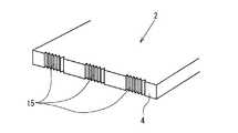
図1は、面状照明装置の分解斜視図である。導光板2の一側端面4に近接して点状光源1が配置されている。点状光源1から出射された光は、導光板2の出射面3から出射して被照明体20側に導かれるように構成されている。点状光源1は、例えば、LEDチップがケースによって覆われ、ケースには出射窓が形成されていて、出射窓から一方向へ出射光が効率よく出射されるように構成されている。以下、出射光が効率よく出射される前記LEDの一方向をLEDの正面側という。点状光源(LED)1は、この正面側が導光板2の一側端面4に対向するように配置される。導光板2の一側端面4のことを、以下、入射面4ともいう。LED1から出射された光は、効率よくこの入射面4へ入射する。LEDチップから出射された光の一部は、LEDチップがケースによって覆われているが、LEDの正面側以外の面、例えば、LEDの上面、下面、左右側面側から漏れ光となって放射される。DESCRIPTION OF EXEMPLARY EMBODIMENTS Hereinafter, an embodiment of a planar lighting device according to the invention will be described with reference to the accompanying drawings.
FIG. 1 is an exploded perspective view of the planar lighting device. A
導光板2は、ポリカーボネート、ポリエステル、ポリメチルメタクリレール、ガラス等の透明性の良好な材料から成り、その裏面5、即ち、出射面3と対向する面には、LED1から導光板2内に入射した光を出射面3全体において均一に出射できるように、図示を省略する光反射パターンが形成されている。 The
また、導光板2の入射面4には、図2に示すように導光板2の厚み方向にプリズム15が形成されている。このプリズム15は、導光板2の入射面4全体、あるいはLED1が配設される位置に、それぞれのLED1の大きさに対応して(入射面4に対向するLED1の幅と略同じ範囲に)形成されている。この構成により出射面3全体の輝度分布を向上させているが、この構成が前述した導光板2の入射面4近傍における、LED近傍の導光板出射面とLED間の導光板出射面との輝度差の発生要因にもなっている。 Further, a
また、導光板2の裏面5側には、裏面5を覆うように反射板6が設けられている。反射板6は、白色樹脂、銀メッキ板等の反射性材料から成り、導光板2の裏面5から外部に放出する光を反射して導光板2内に再入力させるためのものである。従って、この光を反射する部材としては、反射板6に限定されず、例えば、面状照明装置を構成している各部材を一体に保持する液晶ポリマ等からなるハウジングフレームが、反射板の機能を兼ねるように構成してもよい。 Further, a reflective plate 6 is provided on the
導光板2の表側、即ち、出射面3側には、光拡散シート7が設けられている。光拡散シート7は、導光板2に形成されたパターンの形状、例えば、図示を省略する光反射パターンの形状を使用者に視認されないように、光を拡散させるものであり、光拡散剤練込タイプのもの、ランダム凹凸加工タイプのもの等がある。また、光拡散シート7は、通常10μm以上の厚さのもの、好ましくは20〜300μmのものが使用される。さらに、光拡散シート7は、透明な樹脂から構成され、その樹脂としては、ポリカーボネート、ポリエステル、ポリメチルメタクリレート等がある。 A
さらに、光拡散シート7の上側には、輝度増大フィルム(Brightness Enhancement Film)8、9が積層して設けられている。この輝度増大フィルム8、9は、透過性に優れたポリエステル、アクリル樹脂等の表面にプリズムパターンを精密形成した光学フィルムから成る。このように微細なプリズム構造が並ぶフィルムを導光板2の出射面3の上側に配置させることで、被照明体側に放射される光の輝度を向上させることができる。プリズム構造が90度公差する方向に輝度増大フィルム8、9を2枚重ね合わせることで性能が向上し、画面のにじみを解消して、光った部分と光を拡散する部分の縞模様(リフレクティブモアレ)を抑制する作用をなす。 Further, on the upper side of the
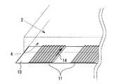
また、導光板2の出射面3側には、反射シート10が設けられている。反射シート10は、導光板2の入射面4側の一部の領域(入射面近傍の領域)と、LED1の上面を覆うように設けられる。また、その形状は、横長の矩形状を有し、長手方向の幅は、導光板2の幅と同じ幅に設定されており、導光板2の入射面近傍の左端から右端までの一面を覆うことができる。反射シート10の裏側、即ち、導光板2の出射面3と向い合う側の面には、光分散部11が設けられている。光分散部11は、導光板2の入射面4に近接配置されているLED1の上面を覆うように、それぞれのLED1に対応した複数箇所に設けられている。 A
上記のように光拡散シート7、輝度増大フィルム8、9、反射シート10等が設けられた導光板2の上側(出射面3側)には、被照明体として、例えば、液晶表示装置20が配置される。液晶表示装置20は、液晶表示素子が配設された表示領域21と、液晶表示素子が配設されていない周辺部である非表示領域22から構成されている。液晶表示装置20は、導光板2の出射面3から出射された光によって、液晶表示装置20の裏側から照射される、いわゆるバックライト型の表示装置である。これにより液晶表示装置20の輝度は向上し、視認性が向上する。 As described above, for example, a liquid
図3は、導光板2の出射面3側に設けられた反射シート10を示す拡大図である。尚、導光板2の入射面4に近接配置されているLED1を破線で示している。また、導光板2の出射面3側に配置される液晶表示装置20の、表示領域21と非表示領域22との境界線を破線12で示している。 FIG. 3 is an enlarged view showing the
反射シート10は、導光板2の入射面4近傍で、導光板2の左端から右端までの領域一面と、LED1の上面を覆うように設けられている。導光板2の入射面4近傍とは、導光板2の出射面3側に配設される液晶表示装置20の非表示領域22のうち、導光板2のLED1が配置されている側の非表示領域の一部分を指している。以下、この導光板2の入射面4近傍のことをLED側非表示領域22'という。また、LED1方向に設けられている反射シート10は、LED1の上面を覆うだけでなく、LED1の周辺の領域も覆うような大きさ及び位置に設けられている。反射シート10は、その位置が移動しないように、図示は省略される導光板2用のハウジングフレーム、あるいは面状照明装置用のハウジングフレーム等に設けた爪部に係止される。尚、この反射シート10の固定手段に関しては特に限定されるものではなく、設けられた位置が変動しなければこの他、粘着テープ等によって固定するようにしてもよい。 The
反射シート10は、反射性の強い白色樹脂から構成されるものであり、上記のような位置に設けることにより、LED1の上面側から漏れる光を反射シート10で反射して、その反射した光を導光板2ヘの入射光として使用することができるので、光源からの光を効率よく利用でき、導光板2の出射面3から出射される光の輝度、即ち、液晶表示装置20の輝度を向上させることができる。 The
尚、反射シート10の形状はこの形態のものに限定されず、導光板2の形状、あるいはLED1(LED以外の点状光源も含む)の形状およびその配置に応じて、LED1から放出される光を効率よく反射できるように、例えば、楕円形、円形、正方形等、適宜選択されるものであってもよい。また、反射シート10の設けられる位置も、LED1の上面側、即ち、導光板2の出射面3側に限定されず、LED1の下面側、即ち、導光板2の出射面3に対向する裏面5側、あるいはLED1の上面及び下面の両側、即ち、導光板2の出射面3および裏面5側に設けられる形態であってもよく、上記同様の作用、効果を得ることができる。 Note that the shape of the
図4及び図5は、反射シート10に設けられた光分散部11を示す拡大図である。図4において、導光板2の入射面4に近接配置され、光分散部11によって覆われるLED1を破線で示している。また、図5において、光分散部11によって入射面4近傍が覆われる導光板2を破線で示している。 4 and 5 are enlarged views showing the
光分散部11は、それぞれのLED1に対応してLED1の上面を覆うように設けられている。光分散部11は、反射シート10の短手方向(図において矢印S方向)には、反射シート10の幅と同じ幅で設けられている。また、長手方向(図において矢印L方向)には、LED1の幅(図において矢印L方向の幅)よりも大きい幅に設けられている。即ち、光分散部11は、LED1の上面だけでなく、LED1の周辺の領域も覆うような大きさ及び位置に設けられている。光分散部11は、反射シート10に対して接着剤等の手段により固定されるが、反射シート10に直接、光分散部11を形成した構成であってもよい。 The
光分散部11は、例えば、複数のプリズムが配列されたプリズムシートから構成されている。さらに具体的には、それぞれのプリズムは、その断面形状が三角形状を有している。プリズムの頂角13がLED1の上面方向、および導光板2の出射面3方向を指すように形成され、また、プリズム列の稜線(図5における矢印14)が導光板2の入射面4に直交するように形成されている。プリズムの頂角13は、90度に形成され、隣接するプリズム間の距離(プリズムピッチ)は、約25μmに形成されている。 For example, the
またこの他、光分散部11は、形成するプリズムの位置によって頂角13の角度が変化するように形成してもよい。例えば、プリズム列の中央部では頂角13を略90度に形成し、周辺部に向かうに従って頂角13が大きくなるように形成してもよい。さらに、頂角13の向きあるいは導光板2の入射面4に対するプリズム列の稜線の角度を、中央部と周辺部とで変化するように形成してもよい。 In addition, the
このように光分散部11としてプリズムシートを使用することにより、LED1の上面からの漏れ光を、プリズムによって反射シート10の長手方向に分散させ、液晶表示装置20の表示領域21のうちLED側非表示領域22近傍に発生していた輝度ムラ、即ち、LED1が配置されている部分で輝度が高く、LED1間の部分で輝度が低くなる輝度ムラを防止すると共に、光を効率良く利用し出射面3全体の高輝度化を図ることができる。 In this way, by using the prism sheet as the
光分散部11は、図示を省略するが、例えば、光拡散部材である光拡散シートから構成されるものであってもよい。この場合、光拡散部材のヘーズ値は80%以上、全光線透過率は90%以上のものを使用することが望ましい。光分散部11として光拡散部材を使用した場合にも、LED1の上面からの漏れ光を分散させることができ、上記同様に液晶表示装置20の表示領域21のうちLED側非表示領域22近傍に発生していた輝度ムラを防止すると共に、光を効率良く利用し出射面3全体の高輝度化を図ることができる。 Although not shown in the drawings, the
反射シート10及び光分散部11の具体的形状としては、例えば、35mm×45mmの大きさの導光板2と、3mmの幅(図において矢印L方向の幅)のLED1を使用した場合には、35mm×6mm程度の大きさの反射シート10、及び5mm×6mm程度の大きさの光分散部11を使用することが好ましい。なお、光分散部11の効果を実験により確認したところ、反射吸収シートを用いた場合と比較して、LED近傍の輝度ムラが同程度に改善され、光分散部11にプリズムシートを用いた場合には、導光板出射面全体における平均輝度が3.5%ほど向上し、光分散部11に光拡散シート(ヘーズ値87%、全光線透過率99%)を用いた場合には、導光板出射面全体における平均輝度が3.1%ほど向上した。 As specific shapes of the
さらに、上記形態では、反射シート10はLED1及び導光板2の一部を覆う大きさ、形状のものを使用したが、この形態に限定されず、導光板2の出射面3上に設けられる光拡散シート7と一体に形成して、その一体化した反射シートによってLED1の上面を覆うようにしてもよい。この場合、光拡散シート7をLED1の上面をも覆う大きさに形成し、反射シートに相当する範囲の所定位置に白色印刷を施すことにより、光拡散部材からなる光分散部を有し、光拡散シート7と一体化された反射シートを容易に作製することができる。また、光分散部11は、導光板2の出射面4上に設けられる輝度増大フィルム8、9の一部を光分散部11の形状に加工して、一体に形成したもの(プリズム)を使用する形態であってもよい。この形態であっても、上記形態と同様の作用、効果を得ることができる。 Furthermore, in the said form, although the
以上のような構成を有することにより、出射面3全体の輝度を均一にすることができるので、LED1近傍の出射面3から出射される光も液晶表示装置20の照明手段(バックライト)として使用できる。従って、LED側非表示領域22を小さくすることができ液晶表示装置20の表示領域21を大型化することができる。 By having the configuration as described above, the luminance of the entire emission surface 3 can be made uniform, so that the light emitted from the emission surface 3 in the vicinity of the
1 点状光源(LED)
2 導光板
3 出射面
4 入射面
5 裏面
6 反射板
7 光拡散シート
8、9 輝度増大フィルム
10 反射シート
11 光分散部
13 頂角
14 プリズム列の稜線方向
1 Point light source (LED)
2 Light guide plate 3
Claims (4)
Translated fromJapanese前記導光板の出射面またはその出射面と対向する面のいずれか一方の面、または両方の面に、前記導光板の入射面近傍と前記点状光源とを覆うように反射シートが設けられ、該反射シートの前記点状光源を覆う部位にプリズム列からなる光分散部が形成され、前記プリズム列の稜線は前記入光面に対して直交する方向に延びていることを特徴とする面状照明装置。In the sidelight type planar illumination device that emits the emitted light from the point light source arranged on the incident surface of the light guide plate from the exit surface of the light guide plate,
Areflective sheet is provided to cover the vicinity of the incident surface of the light guide plate and the point light source on either or both of the exit surface of the light guide plate or the surface facing the exit surface, light dispersion unitcomprising a prism row on site that covers the point light sourceof the reflective sheet isformed, the planarridge of the prism rows, characterized inthat extending in a direction orthogonal to the light incident surface Lighting device.
Priority Applications (5)
| Application Number | Priority Date | Filing Date | Title |
|---|---|---|---|
| JP2004053959AJP4075000B2 (en) | 2004-02-27 | 2004-02-27 | Surface lighting device |
| CNA2004800420784ACN1922436A (en) | 2004-02-27 | 2004-08-27 | flat lighting device |
| US10/590,112US20070165419A1 (en) | 2004-02-27 | 2004-08-27 | Spread illuminating apparatus having light reflecting sheet with light diffusing portions |
| PCT/JP2004/012391WO2005083319A1 (en) | 2004-02-27 | 2004-08-27 | Planar illuminator |
| KR1020067017176AKR20060126577A (en) | 2004-02-27 | 2004-08-27 | A planar lighting device |
Applications Claiming Priority (1)
| Application Number | Priority Date | Filing Date | Title |
|---|---|---|---|
| JP2004053959AJP4075000B2 (en) | 2004-02-27 | 2004-02-27 | Surface lighting device |
Publications (2)
| Publication Number | Publication Date |
|---|---|
| JP2005243522A JP2005243522A (en) | 2005-09-08 |
| JP4075000B2true JP4075000B2 (en) | 2008-04-16 |
Family
ID=34908772
Family Applications (1)
| Application Number | Title | Priority Date | Filing Date |
|---|---|---|---|
| JP2004053959AExpired - Fee RelatedJP4075000B2 (en) | 2004-02-27 | 2004-02-27 | Surface lighting device |
Country Status (5)
| Country | Link |
|---|---|
| US (1) | US20070165419A1 (en) |
| JP (1) | JP4075000B2 (en) |
| KR (1) | KR20060126577A (en) |
| CN (1) | CN1922436A (en) |
| WO (1) | WO2005083319A1 (en) |
Families Citing this family (31)
| Publication number | Priority date | Publication date | Assignee | Title |
|---|---|---|---|---|
| JP2007080544A (en)* | 2005-09-09 | 2007-03-29 | Citizen Electronics Co Ltd | Lighting device |
| JP4775578B2 (en) | 2006-10-26 | 2011-09-21 | ミネベア株式会社 | Surface lighting device |
| TWI324278B (en)* | 2006-12-06 | 2010-05-01 | Au Optronics Corp | Backlight module |
| CN101358710B (en)* | 2007-08-03 | 2012-02-29 | 北京京东方光电科技有限公司 | Back light source device for LED |
| US8047697B2 (en) | 2007-09-10 | 2011-11-01 | Sharp Kabushiki Kaisha | Backlight |
| JP4941189B2 (en)* | 2007-09-12 | 2012-05-30 | エプソンイメージングデバイス株式会社 | LIGHTING DEVICE, LIQUID CRYSTAL DEVICE, AND ELECTRONIC DEVICE |
| CN101393709A (en)* | 2007-09-21 | 2009-03-25 | 富士迈半导体精密工业(上海)有限公司 | billboard |
| WO2009099219A1 (en)* | 2008-02-07 | 2009-08-13 | Sony Corporation | Light guide plate, surface illumination device, liquid crystal display device, and manufacturing method for the light guide plate |
| KR101450810B1 (en)* | 2008-06-02 | 2014-10-14 | 삼성디스플레이 주식회사 | Backlight assembly and display device having same |
| CN101285963B (en)* | 2008-06-06 | 2010-04-07 | 友达光电股份有限公司 | Backlight module |
| KR100975770B1 (en)* | 2008-06-30 | 2010-08-17 | 주식회사 에이엘 | Hinge type waterproof lighting panel |
| US20110176064A1 (en)* | 2008-10-15 | 2011-07-21 | Sharp Kabushiki Kaisha | Lighting device, display device and television receiver |
| TW201035641A (en) | 2009-03-19 | 2010-10-01 | Advanced Optoelectronic Tech | Backlight module |
| JP5229040B2 (en)* | 2009-03-24 | 2013-07-03 | 株式会社Jvcケンウッド | Illumination device and liquid crystal display device |
| JP2012113822A (en)* | 2009-03-26 | 2012-06-14 | Stanley Electric Co Ltd | Surface light source device |
| CN101852363B (en)* | 2009-03-31 | 2013-01-16 | 展晶科技(深圳)有限公司 | Back light module |
| KR101725931B1 (en) | 2010-03-24 | 2017-04-12 | 삼성디스플레이 주식회사 | Backlight assembly and display apparatus having the same |
| JP5267531B2 (en)* | 2010-10-01 | 2013-08-21 | オムロン株式会社 | Light guide panel |
| CN102080789B (en)* | 2010-10-28 | 2012-08-15 | 友达光电股份有限公司 | Liquid crystal display and backlight module thereof |
| JP5512506B2 (en) | 2010-12-24 | 2014-06-04 | パナソニック液晶ディスプレイ株式会社 | Liquid crystal display |
| WO2012165248A1 (en)* | 2011-05-30 | 2012-12-06 | シャープ株式会社 | Illuminating apparatus, display apparatus, and television receiver |
| WO2012165247A1 (en)* | 2011-05-30 | 2012-12-06 | シャープ株式会社 | Illumination device, display device, and television receiving device |
| KR101767973B1 (en) | 2011-08-16 | 2017-08-16 | 삼성디스플레이 주식회사 | Backlight assembly |
| EP2597363A1 (en)* | 2011-11-28 | 2013-05-29 | Research In Motion Limited | Light guide apparatus |
| US8746944B2 (en) | 2011-11-28 | 2014-06-10 | Blackberry Limited | Light guide apparatus having a light source and a reflector |
| US9134004B2 (en) | 2012-04-27 | 2015-09-15 | Cerno Llc | Lighting system for art works |
| CN103032766A (en)* | 2012-12-12 | 2013-04-10 | 京东方科技集团股份有限公司 | Backlight module and display device |
| TWI501008B (en)* | 2013-09-06 | 2015-09-21 | Lextar Electronics Corp | Backlight module |
| KR20190079741A (en)* | 2017-12-27 | 2019-07-08 | 삼성디스플레이 주식회사 | Display appratus including backlight unit and method for manufacturing backlight unit |
| JP7297071B2 (en)* | 2019-08-27 | 2023-06-23 | 三菱電機株式会社 | lighting equipment |
| TWI723796B (en)* | 2020-03-06 | 2021-04-01 | 瑞儀光電股份有限公司 | Light source assembly, backlight module, and display device |
Family Cites Families (7)
| Publication number | Priority date | Publication date | Assignee | Title |
|---|---|---|---|---|
| JPH11258600A (en)* | 1998-03-10 | 1999-09-24 | Denso Corp | Surface light source device for liquid crystal panel |
| US6164790A (en)* | 1998-12-17 | 2000-12-26 | Lg. Philips Lcd Co., Ltd. | Back light unit for a liquid crystal display device |
| JP2003141918A (en)* | 2001-11-01 | 2003-05-16 | Sanyo Electric Co Ltd | Plane light source device |
| JP2003242817A (en)* | 2002-02-13 | 2003-08-29 | Matsushita Electric Ind Co Ltd | Backlight device |
| JP2003331628A (en)* | 2002-03-05 | 2003-11-21 | Seiko Epson Corp | Lighting device, liquid crystal device and electronic equipment |
| JP2003331629A (en)* | 2002-03-05 | 2003-11-21 | Seiko Epson Corp | Lighting device, liquid crystal device and electronic equipment |
| US7226197B2 (en)* | 2002-04-22 | 2007-06-05 | Mitsubishi Rayon Co., Ltd. | Surface light source device and light guide used therefor |
- 2004
- 2004-02-27JPJP2004053959Apatent/JP4075000B2/ennot_activeExpired - Fee Related
- 2004-08-27USUS10/590,112patent/US20070165419A1/ennot_activeAbandoned
- 2004-08-27CNCNA2004800420784Apatent/CN1922436A/enactivePending
- 2004-08-27WOPCT/JP2004/012391patent/WO2005083319A1/enactiveApplication Filing
- 2004-08-27KRKR1020067017176Apatent/KR20060126577A/ennot_activeWithdrawn
Also Published As
| Publication number | Publication date |
|---|---|
| US20070165419A1 (en) | 2007-07-19 |
| CN1922436A (en) | 2007-02-28 |
| JP2005243522A (en) | 2005-09-08 |
| WO2005083319A1 (en) | 2005-09-09 |
| KR20060126577A (en) | 2006-12-07 |
Similar Documents
| Publication | Publication Date | Title |
|---|---|---|
| JP4075000B2 (en) | Surface lighting device | |
| JP3322579B2 (en) | Sidelight type surface light source device | |
| JP2004186000A (en) | Surface light source device and display device | |
| JP2004199967A (en) | Planar light source device, liquid crystal display device, and display device | |
| JP2001312213A (en) | Back light unit, liquid crystal display device, and method for manufacturing light guide plate | |
| US20060274551A1 (en) | Surface light source device and display | |
| JP3835770B2 (en) | Surface light source device | |
| WO2009104793A1 (en) | Light guide body, backlight system and portable terminal | |
| JP4523530B2 (en) | Surface light source device and display device | |
| JP2000231814A (en) | Planar lighting system | |
| JP4552082B2 (en) | Surface lighting device | |
| JP2005228535A (en) | Planar light source device and liquid crystal display device | |
| JP2000082313A (en) | Side light type plane light source device and liquid crystal display device | |
| JP2009140905A (en) | Light guide plate and backlight | |
| WO2014038312A1 (en) | Light source module, lighting module and lighting device | |
| JPH09243828A (en) | Side light type surface light source device | |
| KR20190044870A (en) | Display apparatus | |
| JP4147776B2 (en) | Backlight for LCD | |
| WO2010125839A1 (en) | Lighting device and displaying device | |
| JP2010245005A (en) | Surface light source | |
| US8147112B2 (en) | Backlight assembly and liquid crystal display having the same | |
| JP2006120406A (en) | Lighting device | |
| KR20200015110A (en) | Display apparatus | |
| JP2007080800A (en) | Light guide plate of backlight unit | |
| JP2006331834A (en) | Surface light source device and display device |
Legal Events
| Date | Code | Title | Description |
|---|---|---|---|
| A131 | Notification of reasons for refusal | Free format text:JAPANESE INTERMEDIATE CODE: A131 Effective date:20070815 | |
| A521 | Written amendment | Free format text:JAPANESE INTERMEDIATE CODE: A523 Effective date:20071004 | |
| TRDD | Decision of grant or rejection written | ||
| A01 | Written decision to grant a patent or to grant a registration (utility model) | Free format text:JAPANESE INTERMEDIATE CODE: A01 Effective date:20080109 | |
| A61 | First payment of annual fees (during grant procedure) | Free format text:JAPANESE INTERMEDIATE CODE: A61 Effective date:20080117 | |
| R150 | Certificate of patent or registration of utility model | Free format text:JAPANESE INTERMEDIATE CODE: R150 | |
| FPAY | Renewal fee payment (event date is renewal date of database) | Free format text:PAYMENT UNTIL: 20110208 Year of fee payment:3 | |
| FPAY | Renewal fee payment (event date is renewal date of database) | Free format text:PAYMENT UNTIL: 20120208 Year of fee payment:4 | |
| FPAY | Renewal fee payment (event date is renewal date of database) | Free format text:PAYMENT UNTIL: 20120208 Year of fee payment:4 | |
| FPAY | Renewal fee payment (event date is renewal date of database) | Free format text:PAYMENT UNTIL: 20130208 Year of fee payment:5 | |
| FPAY | Renewal fee payment (event date is renewal date of database) | Free format text:PAYMENT UNTIL: 20140208 Year of fee payment:6 | |
| R250 | Receipt of annual fees | Free format text:JAPANESE INTERMEDIATE CODE: R250 | |
| R250 | Receipt of annual fees | Free format text:JAPANESE INTERMEDIATE CODE: R250 | |
| R250 | Receipt of annual fees | Free format text:JAPANESE INTERMEDIATE CODE: R250 | |
| LAPS | Cancellation because of no payment of annual fees |