JP4073799B2 - Memory system - Google Patents
Memory systemDownload PDFInfo
- Publication number
- JP4073799B2 JP4073799B2JP2003030292AJP2003030292AJP4073799B2JP 4073799 B2JP4073799 B2JP 4073799B2JP 2003030292 AJP2003030292 AJP 2003030292AJP 2003030292 AJP2003030292 AJP 2003030292AJP 4073799 B2JP4073799 B2JP 4073799B2
- Authority
- JP
- Japan
- Prior art keywords
- data block
- data
- controller
- area
- memory system
- Prior art date
- Legal status (The legal status is an assumption and is not a legal conclusion. Google has not performed a legal analysis and makes no representation as to the accuracy of the status listed.)
- Expired - Fee Related
Links
- 238000000034methodMethods0.000claimsdescription57
- 238000006467substitution reactionMethods0.000claimsdescription48
- 238000012937correctionMethods0.000claimsdescription38
- 238000012545processingMethods0.000claimsdescription32
- 239000000872bufferSubstances0.000claimsdescription18
- 238000003860storageMethods0.000claimsdescription18
- 230000004044responseEffects0.000claimsdescription11
- 238000007689inspectionMethods0.000claims1
- 230000010365information processingEffects0.000description30
- 238000012546transferMethods0.000description11
- 230000006866deteriorationEffects0.000description10
- 238000010586diagramMethods0.000description6
- 230000000694effectsEffects0.000description3
- 239000004065semiconductorSubstances0.000description3
- 230000015572biosynthetic processEffects0.000description2
- 230000000052comparative effectEffects0.000description2
- 230000007547defectEffects0.000description2
- 239000007924injectionSubstances0.000description2
- 238000004519manufacturing processMethods0.000description2
- 238000007430reference methodMethods0.000description2
- 229910052581Si3N4Inorganic materials0.000description1
- 239000012141concentrateSubstances0.000description1
- 239000004020conductorSubstances0.000description1
- 238000001514detection methodMethods0.000description1
- 238000005516engineering processMethods0.000description1
- 239000002784hot electronSubstances0.000description1
- 238000002347injectionMethods0.000description1
- 239000011159matrix materialSubstances0.000description1
- 238000005457optimizationMethods0.000description1
- 230000002093peripheral effectEffects0.000description1
- HQVNEWCFYHHQES-UHFFFAOYSA-Nsilicon nitrideChemical compoundN12[Si]34N5[Si]62N3[Si]51N64HQVNEWCFYHHQES-UHFFFAOYSA-N0.000description1
Images


Classifications
- G—PHYSICS
- G11—INFORMATION STORAGE
- G11C—STATIC STORES
- G11C29/00—Checking stores for correct operation ; Subsequent repair; Testing stores during standby or offline operation
- G—PHYSICS
- G11—INFORMATION STORAGE
- G11C—STATIC STORES
- G11C16/00—Erasable programmable read-only memories
- G11C16/02—Erasable programmable read-only memories electrically programmable
- G11C16/06—Auxiliary circuits, e.g. for writing into memory
- G11C16/34—Determination of programming status, e.g. threshold voltage, overprogramming or underprogramming, retention
- G11C16/349—Arrangements for evaluating degradation, retention or wearout, e.g. by counting erase cycles
Landscapes
- Techniques For Improving Reliability Of Storages (AREA)
- For Increasing The Reliability Of Semiconductor Memories (AREA)
- Memory System (AREA)
- Information Retrieval, Db Structures And Fs Structures Therefor (AREA)
- Read Only Memory (AREA)
Description
Translated fromJapanese【0001】
【発明の属する技術分野】
本発明は、不揮発性のメモリシステムに関し、例えばフラッシュメモリカード及びハードディスク互換のフラッシュディスクなどに適用して有効な技術に関する。
【0002】
【従来の技術】
フラッシュメモリに代表される電気的に書換え可能な不揮発性メモリに対する記憶情報の書き換えではメモリセルに電気的なストレスがかり、書き換え回数が増すに従ってメモリセルの特性が劣化する。このため、前記不揮発性メモリには特性を保証することができる書換え可能回数を定めるのが一般的である。書き換えは一部のデータブロックに局在化する場合が有り、一部のデータブロックが書換え可能回数に達したら、当該データブロックを代替エリアに有る未使用メモリブロックと入れ替える技術が提供されている(特許文献1,2参照)。
【0003】
また、各データブロックにおけるECCによる訂正回数をカウントし、ある一定値に達したらそのデータブロックを代替エリアに有る未使用データブロックと入れ替える技術が有る(特許文献3参照)。
【0004】
また、局所的に書き込みが集中すると一部のデータブロックだけ特性劣化が著しくなるので、ある一定の書き換え回数に至ると、自動的に書き換え回数の少ない領域との間でデータとアドレスの入れ替えを行って、不揮発性メモリの書き換え回数寿命を延ばすようにした技術が有る。例えば書き込み回数が規定値を超えるとデータブロックのアドレス割り当てを変更する(特許文献4参照)。またECCエラー回数が規定値を超えるとデータブロックのアドレス割り当てを変更する(特許文献5参照)。
【0005】
【特許文献1】
特開平08−96589
【特許文献2】
特開平2001−229069
【特許文献3】
WO 01/22232
【特許文献4】
特開平04−503720
【特許文献5】
特開平02−118997
【0006】
【発明が解決しようとする課題】
本発明者はフラッシュメモリなどの不揮発性メモリにおけるデータブロックの代替処理について検討した。特に、本発明者はフラッシュメモリなどの不揮発性メモリを適用した大容量且つ高速のフラッシュメモリカードやフラッシュディスクといったハードディスク互換の大容量ストレージについて検討した。
【0007】
第1は、不揮発性メモリのデータブロックに対する代替処理の適正化である。データブロックの書き換え回数が保証値を超えても、必ずメモリセルに特性劣化を生ずるというわけではないから、特許文献1,2のように単に書き換え回数だけでデータブロックの代替を行うと、まだ使用可能なデータブロックを無駄に代替する虞がある。要するに、プロセスバラツキなどによって書換え可能回数には個体差がある。
【0008】
第2は、情報記憶の高信頼性である。特許文献3のようにECCによる訂正回数が規定値に達した場合にデータブロックの代替を行うと、例えば30万回書換え回数を保証しているフラッシュメモリに対して、書換え回数が50万回を超えて始めてECCの訂正が発生してもそのデータブロックには継続して書き換えが可能になる。要するに、特性劣化が進んだ状態で依然として書き換え可能な状態に放置されるデータブロックが存在することになり、情報記憶に対する信頼性を低下させる虞がある。例えば、特性劣化によりECC回路で訂正可能な誤りの発生が頻発すると、これに加えてディスターブなどの影響によるデータ化けを生ずれば、ECC回路による訂正可能なビット数を超えてしまうことが予想され、最早ECC回路の能力では誤りの訂正を行うことができず、記憶データを保護することができなくなる。
【0009】
誤りデータが音声や画像データの場合にはその一部のデータ誤りは他の処理に影響を与えることは少ない。これに対し、演算処理データやプログラムの場合には一部のデータ誤りが他の処理に与える影響が比較的大きく、データ処理の性質によっては致命的な欠陥を生ずる場合もある。従って、ハードディスク互換のフラッシュメモリカードやフラッシュディスク等には特に情報記憶に対する高信頼性が要求される。
【0010】
第3は、高速アクセス処理である。ハードディスク互換のフラッシュメモリカードやフラッシュディスク等に演算処理データやプログラムを格納する場合を想定すると、データ処理を高速化するには、フラッシュメモリカード等は高速アクセス処理が可能でなければならない。書き換え回数寿命を延ばすのにアクセス処理に付随してテーブル参照などが毎回必要になれば、大容量故に、その参照処理がオーバーヘッドになる。例えば特許文献4,5の技術では、データブロックに対するアドレス割り当てを示す対応テーブルをアクセス毎に毎回読み込まなければならない。
【0011】
本発明の目的は、書換え回数寿命を伸ばすのに使用可能なデータブロックを無駄に代替することを抑制可能なメモリシステムを提供することにある。換言すれば、書換え回数寿命を伸ばすのに用意すべき代替用のメモリブロックを少なくすることができるメモリシステムを提供することにある。
【0012】
本発明の別の目的は、特性劣化が進んだデータブロックが依然として書き換え可能な状態に放置されるのを抑制することができ、情報記憶に対する信頼性を向上させることができるメモリシステムを提供することにある。
【0013】
本発明の更に別の目的は、書き換え回数寿命を延ばすのにアクセス処理に付随して毎回テーブル参照などを行わずに済み、高速アクセスを保証して書き換え回数寿命を延ばすことができるメモリシステムを提供することにある。
【0014】
本発明の前記並びにその他の目的と新規な特徴は本明細書の記述及び添付図面から明らかになるであろう。
【0015】
【課題を解決するための手段】
本願において開示される発明のうち代表的なものの概要を簡単に説明すれば下記の通りである。
【0016】
〔1〕本発明の第1の観点は読み出し動作時における代替制御である。この観点によるメモリシステムは、所定の物理アドレス単位に複数のデータブロックを有する不揮発性メモリと、外部からのアクセス要求に応答して前記不揮発性メモリを制御するコントローラとを有する。前記データブロックは夫々のデータ領域に対する書き換え回数とエラー検査情報を保持する領域(31,32)を有する。前記コントローラは前記不揮発性メモリに対する読み出し動作において、読み出し対象領域のデータに対しエラー検査情報によるエラー検査を行い、エラーがあるとき、書き換え回数が所定値を超えていれば別のデータブロックへの代替、超えていなければエラーに係るデータブロック上のデータを訂正する。
【0017】
規定の書き換え回数になっても、素性の良い不揮発性メモリであればまだ書き換えを行うことができる。その指標としてデータブロックのデータ誤り発生状況とその時の書き換え回数とを考慮する。データブロックからの読み出しデータにデータエラーがある時に書き換え回数が所定回数に達していなければECCなどによるエラー訂正を行う。一般にフラッシュメモリなどの不揮発性メモリは、保証する書換え回数の限度内では、メモリ開発メーカが推奨又は指示するエラー訂正能力(エラー訂正可能なビット数)を持てば、訂正不可能な状況は発生しない為、ECC等でエラー訂正されたデータを当該データブロックに書き戻してもデータ信頼度の点では問題ないと考えられるからである。一方、前記データエラーがある時に書き換え回数が所定の回数に達していれば、ECCのエラー訂正能力を超えたビット数のエラーを生ずる虞がそれ以降顕在化すると考えられるので、データブロックを代替し、代替先の新たなデータブロックに訂正データを保持させて利用する。
【0018】
したがって、上記代替手法によれば、ECCとの組み合わせにより書き換え回数が保証限度を超えても代替でき、結果として、単に規定の書き換え回数だけを指標として代替を行う場合に比べて、1データブロックアドレス当たりの平均書換え回数を増やすことができる。このことにより、過剰に代替エリアを持たなくてもよく、また代替処理にかかる処理オーバヘッドを抑制することが出来ることから、高速アクセスを保証することが可能となる。
【0019】
更に、専らECCによるエラー発生回数をデータブロック代替の指標とする場合のように特性劣化が進んだデータブロックが依然として書き換え可能な状態に放置されるのを抑制することができ、情報記憶に対する信頼性を向上させることができる。
【0020】
本発明の具体的な形態として、前記データブロックはその物理アドレスに対応させる論理アドレスの情報保持に利用することが可能なアドレス情報保持領域(30)を有する。このとき、前記コントローラは論理アドレスを物理アドレスとしてデータブロックを選択し、選択したデータブロックの物理アドレスと当該データブロックの前記アドレス情報保持領域が保有する情報との一致により当該データブロックが代替されていないと判定する。したがって、選択したデータブロックの物理アドレスと当該データブロックの前記アドレス情報保持領域が保有する情報との不一致を判別したときだけ、代替先を調べるためのテーブル参照等を行えばよい。アクセス処理に付随して毎回テーブル参照などを行わずに済み、高速アクセスを保証して書き換え回数寿命を延ばすことができる。
【0021】
代替先を調べるためのテーブルとして、前記不揮発性メモリは例えば代替先テーブルを有する。前記代替先テーブルは、物理アドレスの配列順に則して対応する論理アドレス情報の保持に利用されるテーブル情報保持領域(40)を有する。前記コントローラは論理アドレスを物理アドレスとして選択したデータブロックの物理アドレスと当該データブロックの前記アドレス情報保持領域が保有する情報との不一致を判別したとき、物理アドレスに対応するテーブル情報保持領域を参照して、論理アドレスがどのデータブロックで代替されているかを判定することができる。
【0022】
新たな代替先の判別の為に、前記テーブル情報保持領域は論理アドレスの割り当てが行なわれていないデータブロックに対応して未使用コード(USFLG)が格納される。前記コントローラはデータブロックの代替を行うとき前記代替先テーブルを参照し、前記未使用コードに応ずるデータブロックを新たな代替先として判別する。
【0023】
前記アドレス情報保持領域に対して、前記コントローラは論理アドレスの割り当てが行なわれていないデータブロックのアドレス情報保持領域を論理アドレス以外の無効コードにより初期化する。更に前記コントローラはデータブロックの代替を行なうとき、代替元データブロックのアドレス情報保持領域に代替先データブロックの物理アドレスを保持させる。また、前記コントローラは書き換え失敗のデータブロックを消去状態にする。代替されたデータブロックのアドレス情報保持領域に対する取扱を統一し、また、障害発生時などにデータブロックの情報から代替履歴を参照可能にするためである。
【0024】
本発明の具体的な別の形態として、前記複数のデータブロックのうち特定のデータブロックは書き換え閾値回数データ(TDAT)の記憶領域を有する。前記コントローラは、前記書き換え閾値回数データに一致する書き換え回数を前記書き換え回数の所定値と判定する。書き換え可能な回数は半導体製造プロセスに応じてばらつきがあるから、それに則して書き換え回数寿命を伸ばすことが可能になる。
【0025】
不揮発性メモリは例えばフラッシュメモリである。前記論理アドレス情報は32ビット以上である。フラッシュメモリの記憶容量をギガ・ビット以上の大容量化することができる。前記エラー検査情報にはECCコード、CRCコード、パリティコード、及び総積和(SUM値)コードを用いてよい。
【0026】
前記コントローラは、例えば外部インタフェース回路、バッファ、CPU、ECC回路、及びメモリインタフェース回路によって構成すればよい。
【0027】
〔2〕本発明の第2の観点は書き換え動作時における代替制御である。この観点によるメモリシステムでは、前記コントローラは前記不揮発性メモリに対する書き換え動作において、書き換え対象のデータブロックに対する書き換えに失敗したときは書き換え回数が所定値を超えていれば別のデータブロックへの代替、超えていなければ失敗に係るデータブロックに対する再書き換えを行う。前記再書き換えに失敗したときは別のデータブロックへの代替を行う。
【0028】
本発明の第3の観点は書き換え動作時における別の代替制御である。この観点によるメモリシステムは、所定の物理アドレス単位に複数のデータブロックを有する不揮発性メモリと、外部からのアクセス要求に応答して前記不揮発性メモリを制御するコントローラとを有し、前記データブロックはデータ領域に対する書き換え回数とエラー訂正フラグを保持する領域(31,33)を有する。前記コントローラは前記不揮発性メモリに対する書き換え動作において、書き換え対象のデータブロックに対する書き換え回数が所定値を超えていないとき当該データブロックに対する書き換え処理を行い、書き換え回数が所定値を超えているときは当該データブロックのエラー訂正フラグがエラー訂正済みを示していれば別のデータブロックへの代替、エラー訂正済みを示していなければ当該データブロックに対する書き換え処理を行う。前記コントローラは前記不揮発性メモリに対する書き換え処理において、書き換え対象のデータブロックに対する書き換えに失敗したときは書き換え回数が所定値を超えていれば別のデータブロックへの代替、超えていなければ失敗に係るデータブロックに対する再書き換えを行なってよい。前記エラー訂正フラグは例えばエラー訂正が行なわれたか否かを示す1ビット以上のフラグ情報である。
【0029】
第2及び第3の観点による発明の具体的な形態として上記第1の観点の発明と同じ手段を採用して良い。
【0030】
第2及び第3の観点による発明も上記第1の観点の発明と同様に、ECCとの組み合わせにより書き換え回数が保証限度を超えても代替でき、過剰に代替エリアを持たなくても済み、更に、専らECCによるエラー発生回数をデータブロック代替の指標とする場合のように特性劣化が進んだデータブロックが依然として書き換え可能な状態に放置されるのを抑制することができ、情報記憶に対する信頼性を向上させることができる。そして、コントローラは論理アドレスを物理アドレスとしてデータブロックを選択するから、アクセス処理に付随して毎回テーブル参照などを行わずに済み、高速アクセスを保証して書き換え回数寿命を延ばすことができる。
【0031】
【発明の実施の形態】
《フラッシュメモリカード》図1には本発明のメモリシステムの一例であるフラッシュメモリカードが示される。同図に示されるフラッシュメモリカード1は、所定のケーシングに、所定の物理アドレス単位に複数のデータブロック2を有する不揮発性メモリ例えばフラッシュメモリ3と、外部情報処理装置4からのアクセス要求に応答して前記フラッシュメモリ3を制御するコントローラ5とを有する。所定のケーシングは例えばPCカード又は1.8インチのハードディスクのケーシングなどである。外部情報処理装置4はパーソナルコンピュータ、PDA(Personal Digital Assistant)、又はディジタルカメラなどのホスト装置である。データブロック2はデータ領域2Dと管理領域2Cに大別される。
【0032】
前記フラッシュメモリ2は、特に図示はしないが、電気的に消去及び書き込み可能なフラッシュメモリセルをマトリクス配置したメモリセルアレイを有する。このメモリセルアレイに前記複数のデータブロックが構成される。各データブロックは1024ビットのような一定の記憶容量を有し、複数個のフラッシュメモリセルから成る。
【0033】
フラッシュメモリセルには、特に制限されないが、チャンネル領域の上に絶縁膜で分離された導体としてのフローティングゲートに電荷を注入可能にするフローティングゲート構造、或はシリコン窒化膜などの電荷トラップ領域に電荷を局在的に注入可能にする電荷トラップ構造などを採用することができる。例えばフローティングゲート構造の場合には電荷の注入状態と放出状態の閾値電圧の相違に応じて記憶情報の論理値を決める。電荷トラップ構造においては電荷のトラップ位置やトラップ電荷の極性に応じて多値の情報記憶を行なうことが容易である。そのようなフラッシュメモリセルに対するデータの記憶は、例えばメモリセルが保持する電荷を初期的状態にする第1処理(例えばイレーズ処理若しくは消去処理)、初期的状態から電荷状態を変更する第2処理(例えばプログラム処理若しくは書き込み処理)によって行なわれる。例えばフローティングゲート型のフラッシュモリセルのドレインはビット線に、ソースはソース線に、コントロールゲートはワード線に接続される。イレーズ処理はソース線に高電圧を印加して電子をソース線に引き抜く。プログラム処理はワード線に高電圧を印加してドレインからフローティングゲートにホットエレクトロンを注入する。特に制限されないがイレーズ処理はデータブロック単位とされる。
【0034】
前記コントローラ5は、特に制限されないが、外部装置インタフェース回路10、フラッシュメモリインタフェース回路11、マイクロコンピュータ(MPU)12、RAM(ランダムアクセスメモリ)から成るバッファ13、ECC(エラーコレクティングコード)回路14、及び内部バス15を有する。外部装置インタフェース回路10は外部情報処理装置4とのインタフェース制御を行う。例えば外部とのインタフェース仕様は、ハードディスク互換を考慮すればIDE(Integrated Device Electronics)等とされる。フラッシュメモリインタフェース回路11は、フラッシュメモリ3のコマンド及びデータアクセス仕様を満足するフラッシュメモリインタフェース制御を行う。MPU12は中央処理装置(CPU)、CPUのワークRAM、及びCPUの制御プログラムROM等を有し、CPUが制御プログラムを実行して、外部装置インタフェース回路10による外部インタフェース制御、フラッシュメモリインタフェース回路11によるメモリインタフェース制御等を行う。バッファ13は外部情報処理装置4からの書込みデータ、外部情報処理装置4への読み出しデータを一時的に蓄える。
【0035】
本発明の実施形態では、コントローラとメモリを分離しているが、その2つ及び周辺部品を1つにした混載半導体としてもかまわない。
【0036】
外部情報処理装置4から外部装置インタフェース回路10にデータアクセス要求があると、MPU12はアクセス対象データの物理アドレスであるセクタアドレス及びアクセスコマンド等をフラッシュメモリインタフェース回路6からフラッシュメモリ2に与え、フラッシュメモリ2のデータ書き換え動作及びデータ読み出し動作等を制御する。データ書き換え動作は前記イレーズ処理とプログラム処理によって行なわれる。書き換え動作では外部情報処理装置4から供給された書き込みデータがフラッシュメモリ3に与えられる。読み出し動作ではフラッシュメモリ3から読み出されたデータが外部情報処理装置11に出力される。
【0037】
フラッシュメモリ3の各データブロック(例えばセクタとも称する)2にはデータブロックの物理的な配置である物理アドレス(セクタアドレスとも称する)が割当てられる。要するに、アドレス信号をデコードしてデータブロックを選択するためのアドレスデコーダのデコード論理にそのアドレス割り当てが組み込まれている。前記物理アドレスのビット数は例えば32ビットである。外部情報処理装置4はデータブロックの論理的な配置を論理アドレスで管理する。MPU12は外部情報処理装置4が指定する論理アドレスを物理アドレスとしてフラッシュメモリ3のアクセスに利用する。要するに、MPU12は論理アドレスと物理アドレスの対応テーブルを常時参照することを要しないということである。
【0038】
《フラッシュメモリのデータ構造》図2にはフラッシュメモリ3のデータブロックによるデータ構造が例示される。図2ではデータブロック2として例えば物理アドレス0〜zまでのデータブロック2(0)〜2(z)を有し、物理アドレス0〜n−1までのデータブロック2(0)〜2(n−1)はユーザデータ領域20、物理アドレスn〜z−1までのデータブロック2(n)〜2(z−1)は代替領域21、物理アドレスzのデータブロック2(z)は代替先テーブルの形成領域22とされる。各データブロック2には前述の通り物理アドレスが割り当てられ、管理領域2Cとして、論理アドレス領域30、書換え回数領域31、ECCコード領域32を有する。
【0039】
前記論理アドレス領域30は物理アドレスに対応される論理アドレスの情報保持に利用することが可能なアドレス情報保持領域とされる。書換え回数領域31には対応するデータブロック2の書換え回数が保持される。ECCコード領域32は対応するデータブロック2のエラー検査情報としてECCコードを保有する。ECCコードは例えばデータブロック全体に対するECCコードとされる。データ領域だけに対するECCコードであってもよい。論理アドレスの割り当てに利用されていない論理アドレス領域30はコントローラ5により無効コードIVCODが初期的に書込まれる。即ち、物理アドレスzを除く代替領域31の論理アドレス領域30は当初無効コードIVCODを有する。前記物理アドレスzのデータブロック2(z)において論理アドレス領域30にはテーブルフラグが格納され、当該データブロック2(z)のデータ領域には代替先テーブルSTLBが格納される。
【0040】
前記コントローラ5は論理アドレスを物理アドレスとしてデータブロック2を検索し、検索したデータブロック2の物理アドレスと当該データブロックの前記論理アドレス領域30が保有する情報との一致により当該データブロックが代替されていないと判定する。したがって、検索されたデータブロックの物理アドレスと当該データブロックの前記論理アドレス領域30が保有する情報との不一致を判別したときだけ、代替先を調べるために代替先テーブルSTLBの参照等を行えばよい。アクセス処理に付随して毎回代替先テーブルSTLBの参照を行わなくてもよい。
【0041】
本発明の実施形態では、毎回代替先テーブルSTLBを参照する方式を説明する。しかし、代替領域を最小限にすることが本発明では可能なので、テーブルSTLB参照をせずに直接代替領域を検索することも可能である。
【0042】
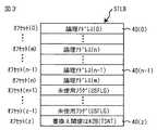
図3には前記代替先テーブルSTLBの一例が示される。代替先テーブルSTLBは、ユーザデータ領域20における不良若しくは書換え寿命が尽きたデータブロック2を代替する代替領域21のデータブロックを調べるためのデータテーブルである。この代替先テーブルSTLBは、物理アドレスの配列順に則してテーブル情報保持領域40、即ち40(0)〜40(z)を有する。テーブル情報保持領域40(0)〜40(z)は物理アドレスの配列順に則して対応する論理アドレス情報の保持に利用される。テーブル情報保持領域40(0)〜40(z)に対応する物理アドレスは当該テーブル情報保持領域のオフセットから得られる。例えば物理アドレス(n−1)に対応する論理アドレス(n−1)は代替先テーブルSTLBのオフセット(n−1)に位置するテーブル情報保持領域40(n−1)から得られる。この代替先テーブルSTLBは、現在の論理アドレスが何処の物理アドレスに割り当てられているか、及び未使用領域は何処にあるのかを示すことができる。
【0043】
前記コントローラ5は論理アドレスを物理アドレスとして検索したデータブロックの物理アドレスと当該データブロックの前記論理アドレス領域30が保有する情報との不一致を判別したとき、前記代替先テーブルSTLBの物理アドレスに対応するテーブル情報保持領域40を参照して、論理アドレスがどのデータブロックで代替されているかを判定することができる。例えば図3に従えば、物理アドレス(n)に対応する論理アドレスは、代替先テーブルSTLBのオフセット(n)に位置するテーブル情報保持領域40(n)の情報より、論理アドレス(m)となる。
【0044】
新たな代替先の判別の為に、前記代替先テーブルSTLBのテーブル情報保持領域40(0)〜40(z(―1))は論理アドレスの割り当てが行なわれていないデータブロックに対応して未使用コードとしての未使用フラグUSFLGが格納される。前記コントローラ5はデータブロックの代替を行うとき前記代替先テーブルSTLBを参照し、前記未使用フラグUSFLGに応ずるデータブロックを新たな代替先と判定する。
【0045】
前記代替先テーブルSTLBのオフセット(z)におけるテーブル情報保持領域40(z)は書き換え閾値回数データTDATの記憶領域40(z)として利用される。コントローラ5はデータブロックの代替可否の判別若しくは書換え寿命の判別にその書き換え閾値回数データTDATを利用する。データブロックの書換え可能回数は半導体製造プロセスに応じてばらつきがあるから、それに則して書き換え回数寿命を判定できるようにするためである。
【0046】
《読出し動作時の代替制御》次に前記データブロックに対する読出し動作時における代替制御について説明する。
【0047】
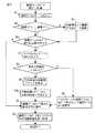
図4にはコントローラによる読出し動作の制御フローが例示される。論理アドレスmのデータ読み出し処理が指示されると、それに応答して物理アドレスmのデータブロックをバッファ13に読み出す(S1)。読み出されたデータブロック2(m)の論理アドレス領域30が保持する論理アドレス情報とデータブロック2(m)の物理アドレスが一致するか否かが判定される(S2)。一致であればデータブロックの代替は行なわれていないと判断される。不一致であればデータブロックの代替が行なわれていると判断され、代替先テーブルSTLBを参照して代替領域21より論理アドレスmのデータブロックを検索して当該データブロックの記憶情報をバッファ13に読み出す(S3)。ステップS2における一致判定に係るデータブロック、又はステップS3で検索された代替データブロックの全データに対してECC回路により誤りの有無を判定する(S4)。本発明では、論理アドレスコードを用いてユーザデータを管理している。しかし、これ以外に例えばS2のチェックでECCコードが訂正無し又は訂正可能であれば、物理アドレスと論理アドレスが一致しているとみなし、訂正不可能であれば代替されているとみなして、代替領域を検索して論理アドレスmを参照する方式でも、本発明を実現することが出来る。誤りがなければコントローラ5は論理アドレスmのユーザデータの転送許可を外部情報処理装置4に要求し(S5)、外部情報処理装置4からの許可を待って論理アドレスmのデータをバッファ13から外部情報処理装置4に転送する(S6)。
【0048】
前記ステップS4の判定にて誤りが有れば、バッファ13上で読み出しデータを訂正する(S7)。そして書き換え回数が書き換え閾値回数データTDATの示す回数(例えばK回)以上であるかの判定が行なわれる(S8)。K回以上でなければバッファ13内の論理アドレスmのデータを訂正して、当該論理アドレスmに対応する物理アドレスのデータブロックに訂正データを書き戻して、フラッシュメモリ3上の対応する記憶データを訂正する。その後、前記ステップS5、S6へ進んで外部情報処理装置4へのデータ転送を行なう。
【0049】
前記ステップS8の判定により書き換え回数がK回以上の場合、代替先テーブルSTLBを参照して代替領域21より未使用のデータブロックを検索する(S9)。検索された未使用データブロックを論理アドレスmの新たなデータブロックとする代替処理を行なう(S10)。この代替処理では、第1に、前記検索された前記未使用データブロックの論理アドレス領域に論理アドレスmの情報を格納し、前記未使用データブロックのデータ領域にユーザデータmを格納し、また、代替前の論理アドレスmのデータブロックの論理アドレス領域に前記未使用データブロックの物理アドレス情報を格納する。第2に、前記代替先テーブルSTLB上のテーブル情報保持領域40に対し、未使用データブロックの物理アドレスに応ずるオフセット位置に論理アドレスmの情報を格納する。その後、前記ステップS5、S6へ進んで外部情報処理装置4へのデータ転送を行なう。
【0050】
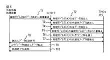
図5には図4の読み出し制御を用いてフラッシュメモリカード1からデータを読み出す動作の全体的なフローチャートが例示される。同図の動作では、読み出し前のフラッシュメモリ3の状態は図2の状態とされ、読み出し後のフラッシュメモリ3の状態は図6の状態、読み出し後の代替先テーブルSTLBの状態は図3の状態とされる。書き換え閾値回数はK回とする。
【0051】
外部情報処理装置4がユーザデータ領域20の特定のデータブロック、例えば論理アドレスmのデータ読み出し要求をコントローラ5に指示する(T1)。これを受けてコントローラ5は、物理アドレスmのデータブロックのデータをフラッシュメモリ3から受取る(T2)。コントローラ5は受取った読み出しデータに対して図4の処理を行なう。この例では、図2の通り、データブロック2(m)の論理アドレス領域30の論理アドレスは物理アドレスmに等しく、また、そのデータブロック2(m)のデータにはECCコードによって訂正可能な誤りが発生しているものとする。更に、データブロック2(m)の書き換え回数は上限K回を超えてK+1回とされている。コントローラ5は代替領域21の未使用データブロックを検索するために物理アドレスzの代替先テーブルSTLBをフラッシュメモリ3から読み込む(T3)。コントローラ5は代替先テーブルSTLBから未使用フラグ(USFLG)を保有するテーブル情報保持領域を検索して、例えばテーブル情報保持領域40(n)を得る。この領域40(n)のオフセットに基づいてコントローラ5は物理アドレス(n)のデータテーブルの情報を読出し、その論理アドレス領域30に無効コードIVCODが格納されていること、ECCコード領域のECCコードに基づいてエラーが無いことを確認する。(T4)。無効コードが格納されていなかったり、ECCコードによる誤りがある場合にはT3,T4の処理を繰り返す。
【0052】
処理T4において無効コードが確認され、ECCコードによる誤りのないことが確認された場合には、代替前の論理アドレスmのデータブロックの論理アドレス領域をアドレス情報nに書き換え(T5)、物理アドレスnのデータブロックの論理アドレス領域に論理アドレスmの情報を格納すると共にそのデータ領域にユーザデータmを書込み(T6)、物理アドレスnに応ずるオフセット位置に論理アドレスmの情報を格納するように前記代替先テーブルSTLBを書き換える(T7)。
【0053】
この後コントローラ5は読出しデータの転送許可を外部情報処理装置4に要求し(T8)、外部情報処理装置4からの許可を待って論理アドレスmのデータ(ユーザデータm)を外部情報処理装置4に転送する(T9)。転送の後、コントローラ5は外部情報処理装置4に読出し処理終了を通知する(T10)。
【0054】
上記読出し動作時の代替制御では、規定の書き換え回数になっても、素性の良い不揮発性メモリであればまだ書き換えを行うことができる、という点に着目している。その指標としてデータブロックのデータに対するECCエラーチェックの結果と書き換え回数とを考慮する。データブロックからの読み出しデータにデータエラーがある時に書き換え回数が規定の閾値に達していなければECCなどによる訂正を行う。一般にフラッシュメモリなどの不揮発性メモリは、保証する書換え回数の限度内では、メモリ開発メーカが推奨又は指示するエラー訂正能力(エラー訂正可能なビット数)を持てば、訂正不可能な状況は発生しない為、ECC等でエラー訂正されたデータを当該データブロックに書き戻してもデータ信頼度の点では問題ないと考えられるからである。一方、前記データエラーがある時に書き換え回数が規定の閾値を超えていれば、ECCのエラー訂正能力を超えたビット数のエラーを生ずる虞がそれ以降顕在化すると考えられるので、データブロックを代替し、代替先の新たなデータブロックに訂正データを保持させて利用する。
【0055】
したがって、上記代替手法によれば、ECCとの組み合わせにより書き換え回数が保証限度を超えても代替でき、結果として、単に規定の書き換え回数だけを指標として代替を行う場合に比べて、1データブロックアドレス当たりの平均書換え回数を増やすことができる。このことにより、過剰に代替エリアを持たなくてもよい。
【0056】
更に、専らECCによるエラー発生回数をデータブロック代替の指標とする場合のように特性劣化が進んだデータブロックが依然として書き換え可能な状態に放置されるのを抑制することができ、情報記憶に対する信頼性を向上させることができる。
【0057】
《書換え動作時における代替制御》次に前記データブロックに対する書換え動作時における代替制御について説明する。
【0058】
図7にはコントローラによる書換え動作の制御フローが例示される。論理アドレスmのデータ書換え処理が指示されると、それに応答してコントローラ5は外部情報処理装置4に論理アドレスmに対する書き換えデータ(ユーザデータmの書き換えデータ)の転送許可を通知する(S11)。コントローラ5はこの許可を受けて外部情報処理装置4が出力する前記書き換えデータを受取ってバッファ13に格納する(S12)。コントローラ5は物理アドレスmのデータブロックをバッファ13に読み出す(S13)。読み出されたデータブロック2(m)の論理アドレス領域30が保持する論理アドレス情報とデータブロック2(m)の物理アドレスが一致するか否かが判定される(S14)。一致であればデータブロックの代替は行なわれていないと判断され、論理アドレスmに応ずる物理アドレスmのデータブロック2(m)におけるデータ領域をバッファ13内のデータで書換える(S15)。不一致であればデータブロックの代替が行なわれていると判断され、代替先テーブルSTLBを参照して論理アドレスmが代替されているデータブロックを検索し(S16)、その代替されているデータブロックにおけるデータ領域をバッファ13内のデータで書換える(S15)。ステップS15の書き換えにおいて、コントローラ5はフラッシュメモリ3より書換え失敗の通知の有無を判定する(S17)。失敗がなければその書き換え処理は終了される。失敗が有るときは、コントローラ5は、そのときの書き換え回数が書き換え閾値回数データTDATの示す回数(例えばK回)以上であるかの判定が行なわれる(S18)。
【0059】
前記ステップS18の判定により書き換え回数がK回以上の場合、代替先テーブルSTLBを参照して代替領域21より未使用のデータブロックを検索する(S19)。検索された未使用データブロックを論理アドレスmの新たなデータブロックとする代替処理を行なう(S20)。この代替処理では、第1に、前記検索された前記未使用データブロックの論理アドレス領域に論理アドレスmの情報を格納し、前記未使用データブロックのデータ領域にバッファ13上の書換え用ユーザデータmを格納し、また、代替前の論理アドレスmのデータブロックの論理アドレス領域に前記未使用データブロックの物理アドレス情報を格納する。第2に、前記代替先テーブルSTLB上のテーブル情報保持領域40に対し、未使用データブロックの物理アドレスに応ずるオフセット位置に論理アドレスmの情報を格納する。コントローラ5は当該代替処理に対してフラッシュメモリ3より書き換え失敗通知が有るか否かを判定し(S21)、なければその書き換え処理を終了する。書き換え失敗であれば再度ステップS19,S20の処理を繰返す。ステップS20の代替処理に対してはリトライ回数の制限、又は書き換え回数によって制限を付しても良く、制限回数に足したときはエラー終了とされる。
【0060】
前記ステップS18の判定により書き換え回数がK回以上でなければコントローラ5はバッファ13内の書換え用ユーザデータmで論理アドレスmのデータ領域に対して再度書き込み処理を行なう(S22)。この書き込みに対してもステップS21で書き込み失敗通知の有無を判定し、失敗であればステップS19,S20の処理が行なわれる。
【0061】
図8には書き換え処理要求に応答するフラッシュメモリの書換えが失敗したときの動作フローチャートが示される。同図の書き換えでは、書き換え前のフラッシュメモリ3の状態は図2の状態とされ、書き換え後のフラッシュメモリ3の状態は図9の状態とされる。書き換え閾値回数はK回とする。
【0062】
外部情報処理装置4から論理アドレスmのデータ書換え処理(T11)、それに応答するコントローラ5から外部情報処理装置4への書き換えデータ(ユーザデータm書き換えデータ)の転送許可通知(T12)、外部情報処理装置4からコントローラ5への前記ユーザデータm書き換えデータの転送処理(T13)が行なわれる。コントローラ5は物理アドレスmのデータブロックをフラッシュッメモリ3から読み出し(T14)、論理アドレスmのデータブロックが代替されていないことを確認して当該物理アドレスmのデータブロックをユーザデータm書き換えデータにより書き換える(T15)。このとき、例えばフラッシュメモリ3は書き換え失敗通知をコントローラ5に発行する(T16)。書き換え回数は上限回数Kを超えているから、データブロックを代替するためにデータブロック2(z)の代替先テーブルSTLBをフラッシュメモリ3から読み出す(T17)。コントローラ5は代替先テーブルSTLBを検索して代替先としてアドレスnのデータブロックを認識し、今度は当該物理アドレスnのデータブロックをフラッシュメモリ3から読み出す(T18)。読み出した物理アドレスnのデータブロックに対してエラー検出などを行ない、正常であればこの物理アドレスnのデータブロックを代替に用いるため、コントローラ5は前述の通り其の代替を反映するために代替先テーブルSTLBを書き換え(T19)、物理アドレスnのデータブロックをユーザデータm書き換えデータで書き換える(T20)。最後にコントローラ5は外部情報処理装置4に処理の終了を通知する(T21)。
【0063】
図8の動作による書き換え処理結果を示す図9において、図2の初期状態のフラッシュメモリの物理アドレスmに対し、図6と比べると、物理アドレスmの書換えが失敗している為、全てのデータが無効になっている。ここでいう無効とは例えば全データが消去状態又はECC訂正不可状態等になっていることを意味する。
【0064】
読み出し動作ではECCエラーが有ったときに書き換え回数を参照してそれが上限を超えている場合にデータブロックの代替を行なった。書き換えの場合は、書き換えに失敗したときに書き換え回数を参照してそれが上限を超えている場合にデータブロックの代替を行なう。これはメモリセルの特性が劣化するに従って書き換え失敗の確率も高くなると考えられるからであり、書き換え失敗のときに書き換え回数が上限を超えていればメモリセルの書き換え回数寿命が尽きるのも真近であると考える。これは、読み出し動作時にECCエラーが有ったとき書き換え回数が上限を超えている場合にはメモリセルの書き換え回数寿命が尽きるのも真近であると考えるのと同様である。したがって、書き換えの場合にも読み出しの場合と同様に、ECCとの組み合わせにより書き換え回数が保証限度を超えても代替でき、過剰に代替エリアを持たなくても済み、更に、専らECCによるエラー発生回数をデータブロック代替の指標とする場合のように特性劣化が進んだデータブロックが依然として書き換え可能な状態に放置されるのを抑制することができ、情報記憶に対する信頼性を向上させることができる。そして、コントローラは論理アドレスを物理アドレスとしてデータブロックを選択するから、アクセス処理に付随して毎回テーブル参照などを行わずに済み、高速アクセスを保証して書き換え回数寿命を延ばすことができる。
【0065】
《書換え動作時における別の代替制御》次に前記データブロックに対する書換え動作時における代替制御の別の例について説明する。
【0066】
図10にはフラッシュメモリ3のデータ構造の別の例が示される。図2のデータ構造との相違点は各データブロック2にECC訂正フラグ領域33を追加したことである。ECC訂正フラグ領域33は対応するデータブロックをリードした時、1回でもECC訂正を行ったことがある場合に訂正有りフラグが立てられる。訂正がなければ訂正無しフラグが立てられている。代替領域21において代替される前のECC訂正フラグ領域33は無効データ、即ち、消去状態にされている。図10の例では、物理アドレスmに以前ECCによる訂正が発生していたことを表している。
【0067】
図11には図10のデータ構造に対するコントローラによる書換え動作の制御フローが例示される。論理アドレスmのデータ書換え処理が指示されると、それに応答してコントローラ5は外部情報処理装置4に論理アドレスmに対する書き換えデータ(ユーザデータmの書き換えデータ)の転送許可を通知する(S30)。コントローラ5はこの許可を受けて外部情報処理装置4が出力する前記書き換えデータを受取ってバッファ13に格納する(S31)。コントローラ5は論理アドレスmのデータブロックを読み出し(S32)、当該データブロックの書き換え回数が上限のK回以上であるか否かを判定する(S33)。K回に達していなければバッファ13が保有するユーザデータm書き換えデータによって論理アドレスmのデータブロックのデータ領域を書き換える(S34)。書き換え回数がK回以上であるときは、その論理アドレスmのデータブロックにECC訂正フラグが立っているか否かを判定する(S35)。ECC訂正フラグが立っていなければステップS34の書き換え処理を行なう。ECC訂正フラグが立っているときはその論理アドレスmのデータブロックを未使用データブロックに代替し、代替先にユーザデータm書き換えデータを書き込む(S36)。
【0068】
特に図示はしないがステップS34にて書き込み失敗のときはステップS36の処理に進めばよい。また、特に図示はしないが、図7における書き換えを失敗したときの処理と、図11におけるECCエラー訂正フラグの有無に応じた処理の双方を行なうことも可能である。
【0069】
図12には図10のデータ構造のフラッシュメモリ3に対して図11の処理にしたがって代替が行なわれた後におけるフラッシュメモリのデータ構造が例示される。物理アドレスmのデータ領域2Dに記憶されていたユーザデータmは物理アドレスnに代替されている。
【0070】
図11の書き換えの場合は、書き換え回数が上限を超えている場合に一度でもECC訂正が行なわれている場合にはデータブロックの代替を行なって書き換えを行なう。これは、読み出し動作時にECCエラーが有ったとき書き換え回数が上限を超えている場合にはメモリセルの書き換え回数寿命が尽きるのも真近であると考えるのと同様である。したがって、図11の書き換えの場合にも読み出しの場合と同様に、ECCとの組み合わせにより書き換え回数が保証限度を超えても代替でき、過剰に代替エリアを持たなくても済み、更に、専らECCによるエラー発生回数をデータブロック代替の指標とする場合のように特性劣化が進んだデータブロックが依然として書き換え可能な状態に放置されるのを抑制することができ、情報記憶に対する信頼性を向上させることができる。そして、コントローラは論理アドレスを物理アドレスとしてデータブロックを選択するから、アクセス処理に付随して毎回テーブル参照などを行わずに済み、高速アクセスを保証して書き換え回数寿命を延ばすことができる。
【0071】
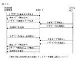
最後に高速アクセスの保証という点について説明を加える。図13には以上説明した本発明による読み出し処理と書き込み処理の動作フローの概略が示される。図14にはある一定の書き換え回数に至ると、自動的に書き換え回数の少ない領域との間でデータとアドレスの入れ替えを行って、不揮発性メモリの書き換え回数寿命を延ばすようにした比較例に係る技術による読み出し処理と書き込み処理の動作フローの概略が示される。図14の場合には、読み出しと書き換えの何れにおいても、論理アドレスと物理アドレスの対応を定義した入れ替えテーブルの参照が必須となる。その意味で図14の動作は常時入れ替え先参照方式とされる。これに対し本発明に係る図13の場合には前述の通り論理アドレスを物理アドレスとしてフラッシュメモリのアクセスを行なうから、代替されているときだけ代替先テーブルを参照すれば足りる。本発明の場合にはテーブル参照という点において高速アクセスも保証されている。
【0072】
以上本発明者によってなされた発明を実施形態に基づいて具体的に説明したが、本発明はそれに限定されるものではなく、その要旨を逸脱しない範囲において種々変更可能であることは言うまでもない。
【0073】
例えば、不揮発性メモリはフラッシュメモリに限定されない。EEPROM、高誘電体メモリ等であってもよい。代替領域の検索方式として代替先テーブルSTLBのようなテーブルを参照する方式に限定されない。そのようなテーブルを用いる代わりに、直接代替領域の論理アドレス領域30を読み出して検索するようにしてもよい。但し検索時間は増える傾向に有ると考えられる。代替領域の未使用データブロックに対しその論理アドレス領域には無効コードIVCODを保持させることに限定されない。単に無効データ等にしておいてもよい。また、図10のデータ構造においてECC訂正フラグ領域33に訂正有りフラグを立てる条件は上記説明に限定されない。所定の複数回ECCによるエラー訂正を行なったことを条件にしてもよい。
【0074】
以上の説明では主として本発明者によってなされた発明をその背景となった利用分野であるハードディスク互換のフラッシュディスク若しくはフラッシュメモリカードに適用した場合について説明したが、本発明はその他種々のメモリシステムに適用することができる。
【0075】
【発明の効果】
本願において開示される発明のうち代表的なものによって得られる効果を簡単に説明すれば下記の通りである。
【0076】
すなわち、メモリシステムにおいて書換え回数寿命を伸ばすのに使用可能なデータブロックを無駄に代替することを抑制することができる。換言すれば、書換え回数寿命を伸ばすのに用意すべき代替用のメモリブロックを少なくすることができる。
【0077】
特性劣化が進んだデータブロックが依然として書き換え可能な状態に放置されるのを抑制することができ、メモリシステムの情報記憶に対する信頼性を向上させることができる。
【0078】
メモリシステムの書き換え回数寿命を延ばすのにアクセス処理に付随して毎回テーブル参照などを行わずに済み、高速アクセスを保証して書き換え回数寿命を延ばすことができる。
【図面の簡単な説明】
【図1】本発明のメモリシステムの一例であるフラッシュメモリカードを示すブロック図である。
【図2】フラッシュメモリのデータブロックによるデータ構造を例示する説明図である。
【図3】代替先テーブルの一例を示す説明図である。
【図4】コントローラによる読出し動作の制御フローを例示するフローチャートである。
【図5】図4の読み出し制御を用いてフラッシュメモリカードからデータを読み出す動作を全体的に示すフローチャートである。
【図6】フラッシュメモリカードからデータを読み出したとき図2のフラッシュメモリのデータ構造の変化の一例を示す説明図である。
【図7】コントローラによる書換え動作の制御フローを例示するフローチャートである。
【図8】外部情報処理装置からの書き換え処理要求に応答するフラッシュメモリの書換えが失敗たときの動作を例示するフローチャートである。
【図9】図8の動作による書き換え処理結果を示す説明図である。
【図10】フラッシュメモリ3のデータ構造としてECC訂正フラグ領域を有する例を示す説明図である。
【図11】コントローラによるECC訂正フラグ領域を参照した書換え動作の制御フローを例示するフローチャートである。
【図12】図10のデータ構造のフラッシュメモリに対して図11の処理にしたがって代替が行なわれた後におけるフラッシュメモリのデータ構造を例示する説明図である。
【図13】本発明による読み出し処理と書き込み処理を概略的に示すフローチャートである。
【図14】常時入れ替え先参照方式による比較例に係る読み出し処理と書き込み処理を概略的に示すフローチャートである。
【符号の説明】
1 フラッシュメモリカード
2 データブロック
2C 管理領域
2D データ領域
3 フラッシュメモリ
4 外部情報処理装置
5 コントローラ
10 外部装置インタフェース回路
11フラッシュメモリインタフェース回路
12 マイクロコンピュータ
13 バッファ
20 ユーザデータ領域
21 代替領域
22 代替先テーブルの形成領域
30 論理アドレス領域
31 書き換え回数領域
32 ECCコード領域
IVCOD 無効コード
STLB 代替先テーブル
40 テーブル情報保持領域
USFLG 未使用フラグ
TDAT 書き換え閾値回数データ
33 ECC訂正フラグ領域[0001]
BACKGROUND OF THE INVENTION
The present invention relates to a nonvolatile memory system, for example, a technique effective when applied to a flash memory card and a hard disk compatible flash disk.
[0002]
[Prior art]
In rewriting stored information in an electrically rewritable nonvolatile memory represented by a flash memory, an electrical stress is applied to the memory cell, and the characteristics of the memory cell deteriorate as the number of rewrites increases. For this reason, the number of rewritable times for which characteristics can be guaranteed is generally determined for the nonvolatile memory. Rewriting may be localized in some data blocks, and when some data blocks reach the maximum number of rewritable times, a technique is provided to replace the data block with an unused memory block in an alternative area ( (See
[0003]
Further, there is a technique of counting the number of times of correction by ECC in each data block and replacing the data block with an unused data block in an alternative area when a certain value is reached (see Patent Document 3).
[0004]
In addition, when writing concentrates locally, the characteristic deterioration of only some data blocks becomes significant. Therefore, when a certain number of rewrites is reached, data and addresses are automatically exchanged between areas with a small number of rewrites. Thus, there is a technique for extending the life of the number of rewrites of the nonvolatile memory. For example, when the number of writes exceeds a specified value, the data block address assignment is changed (see Patent Document 4). When the number of ECC errors exceeds a specified value, the data block address assignment is changed (see Patent Document 5).
[0005]
[Patent Document 1]
JP 08-96589 A
[Patent Document 2]
JP-A-2001-229069
[Patent Document 3]
WO 01/22232
[Patent Document 4]
JP 04-503720
[Patent Document 5]
JP 02-118997
[0006]
[Problems to be solved by the invention]
The inventor has examined alternative processing of data blocks in a nonvolatile memory such as a flash memory. In particular, the present inventor has studied a large-capacity and high-speed storage device compatible with a hard disk such as a high-speed flash memory card or a flash disk to which a nonvolatile memory such as a flash memory is applied.
[0007]
The first is optimization of the substitution process for the data block of the nonvolatile memory. Even if the number of rewrites of the data block exceeds the guaranteed value, the memory cell does not necessarily deteriorate in characteristics. Therefore, if the data block is replaced only by the number of rewrites as in
[0008]
The second is high reliability of information storage. If the data block replacement is performed when the number of corrections by ECC reaches a specified value as in
[0009]
When the error data is voice or image data, some data errors rarely affect other processes. On the other hand, in the case of arithmetic processing data and programs, some data errors have a relatively large effect on other processing, and a fatal defect may occur depending on the nature of the data processing. Therefore, high reliability for information storage is particularly required for hard disk compatible flash memory cards, flash disks, and the like.
[0010]
The third is high-speed access processing. Assuming that arithmetic processing data and programs are stored in a hard disk compatible flash memory card, flash disk or the like, the flash memory card or the like must be capable of high-speed access processing in order to speed up data processing. If it is necessary to refer to the table every time accompanying the access process to extend the lifetime of the rewrite, the reference process becomes an overhead because of the large capacity. For example, in the techniques of
[0011]
An object of the present invention is to provide a memory system capable of suppressing wasteful replacement of a data block that can be used to extend the life of rewrites. In other words, it is an object of the present invention to provide a memory system that can reduce the number of replacement memory blocks that should be prepared for extending the life of the number of rewrites.
[0012]
Another object of the present invention is to provide a memory system that can suppress a data block whose characteristic deterioration has advanced from being left in a rewritable state and improve the reliability of information storage. It is in.
[0013]
Still another object of the present invention is to provide a memory system that can extend the life of the number of rewrites by guaranteeing high-speed access without having to perform table reference every time accompanying the access process to extend the life of the number of rewrites. There is to do.
[0014]
The above and other objects and novel features of the present invention will be apparent from the description of this specification and the accompanying drawings.
[0015]
[Means for Solving the Problems]
The following is a brief description of an outline of typical inventions disclosed in the present application.
[0016]
[1] A first aspect of the present invention is alternative control during a read operation. A memory system according to this aspect includes a nonvolatile memory having a plurality of data blocks in a predetermined physical address unit, and a controller that controls the nonvolatile memory in response to an access request from the outside. The data block has areas (31, 32) for holding the number of rewrites and error check information for each data area. In the read operation to the non-volatile memory, the controller performs error check based on error check information on the data in the read target area, and when there is an error, if the number of rewrites exceeds a predetermined value, it is replaced with another data block If not, the data on the data block related to the error is corrected.
[0017]
Even if the specified number of rewrites is reached, rewriting can still be performed if the nonvolatile memory has a good feature. As the index, the data error occurrence status of the data block and the number of rewrites at that time are considered. If there is a data error in the read data from the data block, if the number of rewrites does not reach the predetermined number, error correction by ECC or the like is performed. In general, non-volatile memory such as flash memory does not cause an uncorrectable situation if it has an error correction capability (number of bits that can be corrected) recommended or specified by the memory developer within the limit of the number of rewrites guaranteed. For this reason, it is considered that there is no problem in terms of data reliability even if data corrected by ECC or the like is written back to the data block. On the other hand, if the number of rewrites reaches a predetermined number when there is a data error, it is considered that the error of the number of bits exceeding the error correction capability of ECC will become apparent thereafter. Then, the corrected data is held in a new data block as a replacement destination and used.
[0018]
Therefore, according to the above alternative method, replacement can be performed even when the number of rewrites exceeds the guaranteed limit by combination with ECC, and as a result, one data block address is compared with the case where replacement is performed using only the specified number of rewrites as an index. The average number of rewrites per hit can be increased. As a result, it is not necessary to have an excessive replacement area, and the processing overhead associated with the replacement processing can be suppressed, so that high-speed access can be guaranteed.
[0019]
Furthermore, it is possible to suppress the data block whose characteristic deterioration has progressed from being left in a rewritable state as in the case where the error occurrence count due to ECC is used as an index for data block substitution, and the reliability of information storage Can be improved.
[0020]
As a specific form of the present invention, the data block has an address information holding area (30) that can be used for holding information of a logical address corresponding to the physical address. At this time, the controller selects a data block using a logical address as a physical address, and the data block is replaced by a match between the physical address of the selected data block and the information held in the address information holding area of the data block. Judge that there is no. Therefore, only when it is determined that there is a discrepancy between the physical address of the selected data block and the information held in the address information holding area of the data block, a table reference or the like for examining the replacement destination may be performed. It is not necessary to refer to the table every time accompanying the access process, and high-speed access can be ensured to extend the life of rewrites.
[0021]
As a table for checking the replacement destination, the nonvolatile memory has, for example, a replacement destination table. The substitution destination table has a table information holding area (40) used for holding corresponding logical address information in the order of arrangement of physical addresses. When the controller determines a mismatch between the physical address of the data block selected as the physical address and the information held in the address information holding area of the data block, the controller refers to the table information holding area corresponding to the physical address. Thus, it is possible to determine in which data block the logical address is replaced.
[0022]
In order to determine a new replacement destination, the table information holding area stores an unused code (USFLG) corresponding to a data block to which no logical address is assigned. The controller refers to the substitution destination table when substituting a data block, and determines a data block corresponding to the unused code as a new substitution destination.
[0023]
For the address information holding area, the controller initializes the address information holding area of the data block to which no logical address is assigned with an invalid code other than the logical address. Further, when the data block is replaced, the controller holds the physical address of the replacement destination data block in the address information holding area of the replacement source data block. In addition, the controller puts the data block that has failed to be rewritten into an erased state. This is because the handling of the address information holding area of the replaced data block is unified, and the replacement history can be referred to from the data block information when a failure occurs.
[0024]
As another specific form of the present invention, a specific data block among the plurality of data blocks has a storage area for rewrite threshold count data (TDAT). The controller determines the number of rewrites that matches the rewrite threshold number data as a predetermined value of the number of rewrites. Since the number of rewritable times varies depending on the semiconductor manufacturing process, it is possible to extend the number of times of rewritable times accordingly.
[0025]
The nonvolatile memory is, for example, a flash memory. The logical address information is 32 bits or more. The storage capacity of the flash memory can be increased to a gigabit or more. For the error check information, an ECC code, a CRC code, a parity code, and a sum of products (SUM value) code may be used.
[0026]
The controller may be constituted by, for example, an external interface circuit, a buffer, a CPU, an ECC circuit, and a memory interface circuit.
[0027]
[2] A second aspect of the present invention is alternative control at the time of rewriting operation. In the memory system according to this aspect, when the controller fails to rewrite the data block to be rewritten in the rewriting operation to the nonvolatile memory, if the number of rewrites exceeds a predetermined value, the controller replaces or exceeds another data block. If not, the data block related to the failure is rewritten. When the rewriting fails, the data is replaced with another data block.
[0028]
The third aspect of the present invention is another alternative control during the rewriting operation. A memory system according to this aspect includes a non-volatile memory having a plurality of data blocks in a predetermined physical address unit, and a controller that controls the non-volatile memory in response to an access request from outside. It has areas (31, 33) for holding the number of rewrites to the data area and an error correction flag. In the rewrite operation for the nonvolatile memory, the controller performs rewrite processing for the data block when the rewrite count for the data block to be rewritten does not exceed a predetermined value, and when the rewrite count exceeds the predetermined value, the data If the error correction flag of the block indicates that the error has been corrected, the data block is replaced with another data block. If the error correction flag does not indicate that the error has been corrected, the data block is rewritten. In the rewriting process for the non-volatile memory, when the controller fails to rewrite the data block to be rewritten, the controller substitutes for another data block if the number of times of rewriting exceeds a predetermined value, and if not, the data related to the failure The block may be rewritten. The error correction flag is, for example, flag information of 1 bit or more indicating whether or not error correction has been performed.
[0029]
As a specific form of the invention according to the second and third aspects, the same means as the invention of the first aspect may be adopted.
[0030]
Similarly to the invention of the first aspect, the inventions according to the second and third aspects can be replaced even when the number of rewrites exceeds the guaranteed limit by combining with ECC, and it is not necessary to have an excessive replacement area. As a result, it is possible to prevent the data block whose characteristic deterioration has progressed from being left in a rewritable state as in the case where the error occurrence count due to ECC is used as an index for data block substitution, and the reliability of information storage can be improved. Can be improved. Since the controller selects the data block using the logical address as the physical address, it is not necessary to refer to the table every time accompanying the access process, and it is possible to guarantee high-speed access and extend the number of rewrites.
[0031]
DETAILED DESCRIPTION OF THE INVENTION
<< Flash Memory Card >> FIG. 1 shows a flash memory card which is an example of the memory system of the present invention. The
[0032]
Although not shown in particular, the
[0033]
The flash memory cell is not particularly limited, but has a floating gate structure that allows a charge to be injected into a floating gate as a conductor separated by an insulating film on the channel region, or a charge trap region such as a silicon nitride film. It is possible to employ a charge trap structure or the like that makes it possible to inject ions locally. For example, in the case of a floating gate structure, the logical value of stored information is determined according to the difference in threshold voltage between the charge injection state and the discharge state. In the charge trap structure, it is easy to store multi-value information according to the charge trap position and the polarity of the trap charge. The storage of data in such a flash memory cell includes, for example, a first process (for example, an erasing process or an erasing process) for setting the charge held in the memory cell to an initial state, and a second process (for example, an erase process or an erasing process). For example, program processing or writing processing). For example, the drain of a floating gate type flash memory cell is connected to a bit line, the source is connected to a source line, and the control gate is connected to a word line. In the erasing process, a high voltage is applied to the source line to extract electrons to the source line. In the program processing, a high voltage is applied to the word line and hot electrons are injected from the drain to the floating gate. Although not particularly limited, the erase process is performed in units of data blocks.
[0034]
The controller 5 is not particularly limited, but includes an external
[0035]
In the embodiment of the present invention, the controller and the memory are separated from each other, but a mixed semiconductor in which the two and peripheral components are combined may be used.
[0036]
When there is a data access request from the external
[0037]
Each data block (also referred to as a sector, for example) 2 of the
[0038]
<< Data Structure of Flash Memory >> FIG. 2 illustrates a data structure of data blocks of the
[0039]
The
[0040]
The controller 5 searches the data block 2 using the logical address as a physical address, and the data block is replaced by a match between the physical address of the searched
[0041]
In the embodiment of the present invention, a method of referring to the substitution destination table STLB every time will be described. However, since it is possible in the present invention to minimize the alternative area, it is possible to directly search for the alternative area without referring to the table STLB.
[0042]
FIG. 3 shows an example of the substitution destination table STLB. The substitution destination table STLB is a data table for examining a data block in the
[0043]
When the controller 5 determines a mismatch between the physical address of the data block searched using the logical address as the physical address and the information held in the
[0044]
In order to determine a new replacement destination, the table information holding areas 40 (0) to 40 (z (-1)) of the replacement destination table STLB are uncorresponding to data blocks to which no logical address is assigned. An unused flag USFLG as a use code is stored. The controller 5 refers to the substitution destination table STLB when substituting the data block, and determines that the data block corresponding to the unused flag USFLG is a new substitution destination.
[0045]
The table information holding area 40 (z) at the offset (z) of the substitution destination table STLB is used as the storage area 40 (z) for the rewrite threshold count data TDAT. The controller 5 uses the rewrite threshold frequency data TDAT for determining whether a data block can be replaced or for determining the rewrite life. This is because the number of times that the data block can be rewritten varies depending on the semiconductor manufacturing process, so that the lifetime of the number of rewrites can be determined accordingly.
[0046]
<< Alternative Control at the Time of Read Operation >> Next, alternative control at the time of read operation for the data block will be described.
[0047]
FIG. 4 illustrates a control flow of the read operation by the controller. When the data read process at the logical address m is instructed, the data block at the physical address m is read out to the
[0048]
If there is an error in the determination in step S4, the read data is corrected on the buffer 13 (S7). Then, it is determined whether the number of rewrites is equal to or greater than the number (for example, K times) indicated by the rewrite threshold number data TDAT (S8). If not more than K times, the data of the logical address m in the
[0049]
If the number of rewrites is K or more as determined in step S8, an unused data block is searched from the
[0050]
FIG. 5 illustrates an overall flowchart of an operation of reading data from the
[0051]
The external
[0052]
When the invalid code is confirmed in the process T4 and it is confirmed that there is no error due to the ECC code, the logical address area of the data block of the logical address m before substitution is rewritten with the address information n (T5), and the physical address n The logical address m information is stored in the logical address area of the data block, and the user data m is written in the data area (T6), and the logical address m information is stored in the offset position corresponding to the physical address n. The destination table STLB is rewritten (T7).
[0053]
Thereafter, the controller 5 requests the external
[0054]
In the alternative control at the time of the read operation, attention is paid to the fact that even if the number of times of rewriting reaches a specified number, rewriting can still be performed with a non-volatile memory having a good feature. As the index, the result of ECC error check for the data of the data block and the number of rewrites are considered. When the data read from the data block has a data error, if the number of rewrites does not reach a specified threshold value, correction by ECC or the like is performed. In general, non-volatile memory such as flash memory does not cause an uncorrectable situation if it has an error correction capability (number of bits that can be corrected) recommended or specified by the memory developer within the limit of the number of rewrites guaranteed. For this reason, it is considered that there is no problem in terms of data reliability even if data corrected by ECC or the like is written back to the data block. On the other hand, if the number of rewrites exceeds the specified threshold when there is a data error, it is considered that the error of the number of bits exceeding the error correction capability of ECC will become apparent thereafter. Then, the corrected data is held in a new data block as a replacement destination and used.
[0055]
Therefore, according to the above alternative method, replacement can be performed even when the number of rewrites exceeds the guaranteed limit by combination with ECC, and as a result, one data block address is compared with the case where replacement is performed using only the specified number of rewrites as an index. The average number of rewrites per hit can be increased. Thus, it is not necessary to have an excessive alternative area.
[0056]
Furthermore, it is possible to suppress the data block whose characteristic deterioration has progressed from being left in a rewritable state as in the case where the error occurrence count due to ECC is used as an index for data block substitution, and the reliability of information storage Can be improved.
[0057]
<< Alternative Control During Rewriting Operation >> Next, alternative control during the rewriting operation for the data block will be described.
[0058]
FIG. 7 illustrates a control flow of the rewriting operation by the controller. When the data rewriting process of the logical address m is instructed, the controller 5 notifies the external
[0059]
If the number of rewrites is equal to or more than K times as determined in the step S18, an unused data block is searched from the
[0060]
If it is determined in step S18 that the number of rewrites is not equal to or greater than K, the controller 5 performs the write process again on the data area of the logical address m with the rewrite user data m in the buffer 13 (S22). Also for this writing, the presence / absence of a writing failure notification is determined in step S21.
[0061]
FIG. 8 shows an operation flowchart when rewriting of the flash memory in response to the rewrite processing request fails. In the rewriting of FIG. 9, the state of the
[0062]
Data rewrite processing (T11) from the external
[0063]
In FIG. 9 showing the result of the rewrite processing by the operation of FIG. 8, the rewrite of the physical address m has failed for the physical address m of the flash memory in the initial state of FIG. Is disabled. Invalid here means, for example, that all data is in an erased state or an ECC correction impossible state.
[0064]
In the read operation, when there is an ECC error, the number of rewrites is referred to, and if it exceeds the upper limit, the data block is replaced. In the case of rewriting, when the rewriting fails, the number of times of rewriting is referred to, and if it exceeds the upper limit, the data block is replaced. This is because the probability of rewrite failure increases as the characteristics of the memory cell deteriorates. If the number of rewrites exceeds the upper limit at the time of rewrite failure, the life of the memory cell rewrite cycle is almost exhausted. I think there is. This is the same as considering that the lifetime of the rewrite frequency of the memory cell is almost exhausted when the rewrite frequency exceeds the upper limit when an ECC error occurs during the read operation. Therefore, in the case of rewriting, as in the case of reading, it can be replaced even if the number of times of rewriting exceeds the guaranteed limit by combining with ECC, and there is no need to have an excessive replacement area. Thus, it is possible to prevent the data block whose characteristic deterioration has progressed from being left in a rewritable state as in the case of using as a data block replacement index, and to improve the reliability of information storage. Since the controller selects the data block using the logical address as the physical address, it is not necessary to refer to the table every time accompanying the access process, and it is possible to guarantee high-speed access and extend the number of rewrites.
[0065]
<< Another Alternative Control During Rewriting Operation >> Next, another example of the alternative control during the rewriting operation for the data block will be described.
[0066]
FIG. 10 shows another example of the data structure of the
[0067]
FIG. 11 illustrates a control flow of a rewrite operation by the controller for the data structure of FIG. When the data rewriting process for the logical address m is instructed, the controller 5 notifies the external
[0068]
Although not shown in particular, if the writing fails in step S34, the process may proceed to step S36. Although not particularly illustrated, it is possible to perform both the processing when the rewriting in FIG. 7 fails and the processing according to the presence or absence of the ECC error correction flag in FIG.
[0069]
FIG. 12 illustrates the data structure of the flash memory after the
[0070]
In the case of the rewriting shown in FIG. 11, if the number of times of rewriting exceeds the upper limit and ECC correction is performed even once, the data block is replaced and rewriting is performed. This is the same as considering that the lifetime of the rewrite frequency of the memory cell is almost exhausted when the rewrite frequency exceeds the upper limit when an ECC error occurs during the read operation. Therefore, in the case of rewriting in FIG. 11 as well as in the case of reading, it can be replaced even if the number of times of rewriting exceeds the guaranteed limit by combining with ECC, and it is not necessary to have an excessive replacement area. It is possible to prevent data blocks whose characteristic deterioration has progressed from being left in a rewritable state as in the case where the number of error occurrences is used as an index for data block substitution, and to improve the reliability of information storage it can. Since the controller selects the data block using the logical address as the physical address, it is not necessary to refer to the table every time accompanying the access process, and it is possible to guarantee high-speed access and extend the number of rewrites.
[0071]
Finally, I will explain the point of ensuring high-speed access. FIG. 13 shows an outline of the operation flow of the read processing and write processing according to the present invention described above. FIG. 14 shows a comparative example in which when a certain number of rewrites is reached, data and addresses are automatically exchanged between areas where the number of rewrites is small, thereby extending the rewrite life of the nonvolatile memory. An outline of the operation flow of read processing and write processing according to the technology is shown. In the case of FIG. 14, in both reading and rewriting, it is essential to refer to a replacement table that defines the correspondence between logical addresses and physical addresses. In this sense, the operation in FIG. 14 is always the replacement destination reference method. On the other hand, in the case of FIG. 13 according to the present invention, since the flash memory is accessed using the logical address as the physical address as described above, it is sufficient to refer to the substitution destination table only when substitution is made. In the case of the present invention, high-speed access is also guaranteed in terms of table reference.
[0072]
Although the invention made by the present inventor has been specifically described based on the embodiments, it is needless to say that the present invention is not limited thereto and can be variously modified without departing from the gist thereof.
[0073]
For example, the nonvolatile memory is not limited to a flash memory. It may be an EEPROM, a high dielectric memory or the like. The search method of the alternative area is not limited to a method of referring to a table such as the alternative destination table STLB. Instead of using such a table, the
[0074]
In the above description, the case where the invention made by the present inventor is applied to a hard disk compatible flash disk or flash memory card, which is the field of use behind the invention, has been described. However, the present invention is applied to various other memory systems. can do.
[0075]
【The invention's effect】
The effects obtained by the representative ones of the inventions disclosed in the present application will be briefly described as follows.
[0076]
That is, it is possible to suppress unnecessary replacement of data blocks that can be used to extend the life of rewrites in the memory system. In other words, it is possible to reduce the number of memory blocks for replacement that should be prepared for extending the life of the number of rewrites.
[0077]
It is possible to prevent the data block whose characteristic deterioration has progressed from being left in a rewritable state, and to improve the reliability of information storage in the memory system.
[0078]
In order to extend the rewrite life of the memory system, it is not necessary to refer to the table every time accompanying the access process, and it is possible to guarantee high speed access and extend the rewrite life.
[Brief description of the drawings]
FIG. 1 is a block diagram showing a flash memory card which is an example of a memory system of the present invention.
FIG. 2 is an explanatory diagram illustrating a data structure of data blocks of a flash memory.
FIG. 3 is an explanatory diagram showing an example of an alternative destination table.
FIG. 4 is a flowchart illustrating a control flow of a read operation by a controller.
FIG. 5 is a flowchart showing an overall operation of reading data from a flash memory card using the read control of FIG. 4;
6 is an explanatory diagram showing an example of a change in the data structure of the flash memory of FIG. 2 when data is read from the flash memory card.
FIG. 7 is a flowchart illustrating a control flow of a rewrite operation by a controller.
FIG. 8 is a flowchart illustrating an operation when rewriting of a flash memory in response to a rewrite processing request from an external information processing apparatus fails.
FIG. 9 is an explanatory diagram showing a rewrite processing result by the operation of FIG. 8;
FIG. 10 is an explanatory diagram showing an example having an ECC correction flag area as a data structure of the
FIG. 11 is a flowchart illustrating a control flow of a rewrite operation with reference to an ECC correction flag area by a controller.
12 is an explanatory view exemplifying the data structure of the flash memory after the replacement of the flash memory having the data structure of FIG. 10 according to the process of FIG. 11;
FIG. 13 is a flowchart schematically showing a read process and a write process according to the present invention.
FIG. 14 is a flowchart schematically showing a read process and a write process according to a comparative example based on a constant replacement destination reference method.
[Explanation of symbols]
1 Flash memory card
2 data blocks
2C management area
2D data area
3 Flash memory
4 External information processing equipment
5 Controller
10 External device interface circuit
11 Flash memory interface circuit
12 Microcomputer
13 buffers
20 User data area
21 Alternative areas
22 Alternative destination table formation area
30 Logical address area
31 Rewrite count area
32 ECC code area
IVCOD invalid code
STLB alternate table
40 Table information holding area
USFLG unused flag
TDAT rewrite threshold frequency data
33 ECC correction flag area
Claims (16)
Translated fromJapanese前記データブロックは夫々のデータ領域に対する書き換え回数とエラー検査情報を保持する領域を有し、
前記コントローラは前記不揮発性メモリに対する読み出し動作において、読み出し対象領域のデータに対しエラー検査情報によるエラー検査を行い、エラーがあるとき、書き換え回数が所定値を超えていれば別のデータブロックへの代替、超えていなければエラーに係るデータブロック上のデータを訂正することを特徴とするメモリシステム。A non-volatile memory having a plurality of data blocks in a predetermined physical address unit, and a controller for controlling the non-volatile memory in response to an access request from the outside,
The data block has an area for holding the number of rewrites and error inspection information for each data area,
In the read operation to the non-volatile memory, the controller performs error check based on error check information on the data in the read target area, and when there is an error, if the number of rewrites exceeds a predetermined value, the data is replaced with another data block A memory system for correcting data on a data block related to an error if not exceeded.
前記データブロックはデータ領域に対する書き換え回数とエラー訂正フラグを保持する領域を有し、
前記コントローラは前記不揮発性メモリに対する書き換え動作において、書き換え対象のデータブロックに対する書き換え回数が所定値を超えていないとき当該データブロックに対する書き換え処理を行い、書き換え回数が所定値を超えているときは当該データブロックのエラー訂正フラグがエラー訂正済みを示していれば別のデータブロックへの代替、エラー訂正済みを示していなければ当該データブロックに対する書き換え処理を行うことを特徴とするメモリシステム。A non-volatile memory having a plurality of data blocks in a predetermined physical address unit, and a controller for controlling the non-volatile memory in response to an access request from the outside,
The data block has an area for holding the number of rewrites to the data area and an error correction flag,
In the rewrite operation for the nonvolatile memory, the controller performs rewrite processing for the data block when the rewrite count for the data block to be rewritten does not exceed the predetermined value, and when the rewrite count exceeds the predetermined value, the data A memory system characterized in that if the error correction flag of a block indicates that the error has been corrected, it is replaced with another data block, and if the error correction flag does not indicate that the error has been corrected, the data block is rewritten.
前記コントローラは論理アドレスを物理アドレスとしてデータブロックを選択し、選択したデータブロックの物理アドレスと当該データブロックの前記アドレス情報保持領域が保有する情報との一致状態により当該データブロックが代替されていないと判定することを特徴とする請求項1乃至6の何れか1項記載のメモリシステム。The data block has an address information holding area that can be used for holding logical address information corresponding to the physical address,
The controller selects a data block using a logical address as a physical address, and the data block is not replaced by a matching state between the physical address of the selected data block and the information held in the address information holding area of the data block. The memory system according to claim 1, wherein the memory system is determined.
前記代替先テーブルは、物理アドレスの配列順に則して対応する論理アドレス情報の保持に利用されるテーブル情報保持領域を有し、
前記コントローラは論理アドレスを物理アドレスとして選択したデータブロックの物理アドレスと当該データブロックの前記アドレス情報保持領域が保有する情報との不一致状態を判別したとき、当該物理アドレスに対応するテーブル情報保持領域を参照して、論理アドレスがどのデータブロックで代替されているかを判定することを特徴とする請求項7記載のメモリシステム。The non-volatile memory has an alternative destination table;
The substitution destination table has a table information holding area used for holding corresponding logical address information in accordance with the arrangement order of physical addresses,
When the controller determines a mismatch between the physical address of the data block selected using the logical address as the physical address and the information held in the address information holding area of the data block, the controller stores the table information holding area corresponding to the physical address. 8. The memory system according to claim 7, wherein it is determined by referring to which data block the logical address is replaced.
前記コントローラはデータブロックの代替を行うとき前記代替先テーブルを参照し、前記未使用コードに応ずるデータブロックを新たな代替先として判別することを特徴とする請求項8記載のメモリシステム。The table information holding area stores unused codes corresponding to data blocks to which logical addresses are not assigned,
9. The memory system according to claim 8, wherein the controller refers to the replacement destination table when replacing a data block, and determines a data block corresponding to the unused code as a new replacement destination.
前記コントローラは、前記書き換え閾値回数データに一致する書き換え回数を前記書き換え回数の所定値と判定することを特徴とする請求項1乃至5の何れか1項記載のメモリシステム。A specific data block among the plurality of data blocks has a storage area for rewrite threshold number of times data,
The memory system according to claim 1, wherein the controller determines that the number of rewrites that matches the rewrite threshold number data is a predetermined value of the number of rewrites.
Priority Applications (7)
| Application Number | Priority Date | Filing Date | Title |
|---|---|---|---|
| JP2003030292AJP4073799B2 (en) | 2003-02-07 | 2003-02-07 | Memory system |
| TW092133429ATW200417860A (en) | 2003-02-07 | 2003-11-27 | Memory system |
| US10/756,292US7137027B2 (en) | 2003-02-07 | 2004-01-14 | Nonvolatile memory system |
| KR1020040006998AKR101056800B1 (en) | 2003-02-07 | 2004-02-03 | Memory system |
| CNA2004100038344ACN1571069A (en) | 2003-02-07 | 2004-02-06 | Nonvolatile memory system |
| US11/583,156US7447936B2 (en) | 2003-02-07 | 2006-10-19 | Nonvolatile memory system |
| US12/245,203US8103899B2 (en) | 2003-02-07 | 2008-10-03 | Nonvolatile memory system |
Applications Claiming Priority (1)
| Application Number | Priority Date | Filing Date | Title |
|---|---|---|---|
| JP2003030292AJP4073799B2 (en) | 2003-02-07 | 2003-02-07 | Memory system |
Publications (2)
| Publication Number | Publication Date |
|---|---|
| JP2004240793A JP2004240793A (en) | 2004-08-26 |
| JP4073799B2true JP4073799B2 (en) | 2008-04-09 |
Family
ID=32820854
Family Applications (1)
| Application Number | Title | Priority Date | Filing Date |
|---|---|---|---|
| JP2003030292AExpired - Fee RelatedJP4073799B2 (en) | 2003-02-07 | 2003-02-07 | Memory system |
Country Status (5)
| Country | Link |
|---|---|
| US (3) | US7137027B2 (en) |
| JP (1) | JP4073799B2 (en) |
| KR (1) | KR101056800B1 (en) |
| CN (1) | CN1571069A (en) |
| TW (1) | TW200417860A (en) |
Families Citing this family (106)
| Publication number | Priority date | Publication date | Assignee | Title |
|---|---|---|---|---|
| US8027194B2 (en) | 1988-06-13 | 2011-09-27 | Samsung Electronics Co., Ltd. | Memory system and method of accessing a semiconductor memory device |
| US7664987B2 (en)* | 2003-05-25 | 2010-02-16 | Sandisk Il Ltd. | Flash memory device with fast reading rate |
| US7173852B2 (en)* | 2003-10-03 | 2007-02-06 | Sandisk Corporation | Corrected data storage and handling methods |
| KR100541642B1 (en)* | 2004-03-11 | 2006-01-10 | 삼성전자주식회사 | Apparatus and method for managing data in flash memory |
| JP2006048783A (en) | 2004-08-02 | 2006-02-16 | Renesas Technology Corp | Nonvolatile memory and memory card |
| JP2006107363A (en)* | 2004-10-08 | 2006-04-20 | Toshiba Corp | Portable electronic device and memory access method used for portable electronic device |
| JP4261462B2 (en)* | 2004-11-05 | 2009-04-30 | 株式会社東芝 | Nonvolatile memory system |
| US7315916B2 (en)* | 2004-12-16 | 2008-01-01 | Sandisk Corporation | Scratch pad block |
| JP2006179101A (en)* | 2004-12-22 | 2006-07-06 | Fujitsu Ltd | Semiconductor memory device |
| US7424648B2 (en)* | 2005-03-10 | 2008-09-09 | Matsushita Electric Industrial Co., Ltd. | Nonvolatile memory system, nonvolatile memory device, data read method, and data read program |
| TWI308741B (en)* | 2005-06-03 | 2009-04-11 | Quanta Storage Inc | A method of defect areas management |
| US20070011513A1 (en)* | 2005-06-13 | 2007-01-11 | Intel Corporation | Selective activation of error mitigation based on bit level error count |
| US7590913B2 (en)* | 2005-12-29 | 2009-09-15 | Intel Corporation | Method and apparatus of reporting memory bit correction |
| KR100744122B1 (en)* | 2006-01-12 | 2007-08-01 | 삼성전자주식회사 | Control method of hybrid hard disk drive, suitable recording medium and suitable device |
| JP2007214786A (en)* | 2006-02-08 | 2007-08-23 | Toshiba Corp | Portable imaging device |
| US20070226401A1 (en)* | 2006-03-21 | 2007-09-27 | Pa-Chung Huang | Data accessing structure and method for flash memory |
| US7286409B1 (en)* | 2006-05-09 | 2007-10-23 | Macronix International Co., Ltd. | Method and apparatus to improve nonvolatile memory data retention |
| KR100854970B1 (en) | 2007-01-08 | 2008-08-28 | 삼성전자주식회사 | Multi-level cell flash memory device and its program method |
| US20080072119A1 (en)* | 2006-08-31 | 2008-03-20 | Rodney Rozman | Allowable bit errors per sector in memory devices |
| KR100802059B1 (en)* | 2006-09-06 | 2008-02-12 | 삼성전자주식회사 | Memory system and method of operation thereof capable of suppressing bad block generation due to read disturb |
| DE102007033746A1 (en) | 2006-10-12 | 2008-04-17 | Giesecke & Devrient Gmbh | Data object managing method for waste memory, involves storing new data object in memory or changing contents of data objects in memory, where check sum is computed and stored in check sum field of data objects |
| US8145983B1 (en) | 2006-11-08 | 2012-03-27 | Marvell International Ltd. | Methods and apparatus for identification of likely errors in data blocks |
| JP4575346B2 (en)* | 2006-11-30 | 2010-11-04 | 株式会社東芝 | Memory system |
| US7929372B2 (en)* | 2007-01-25 | 2011-04-19 | Samsung Electronics Co., Ltd. | Decoder, memory system, and physical position converting method thereof |
| KR100929155B1 (en)* | 2007-01-25 | 2009-12-01 | 삼성전자주식회사 | Semiconductor memory device and memory cell access method thereof |
| KR100877609B1 (en)* | 2007-01-29 | 2009-01-09 | 삼성전자주식회사 | Semiconductor memory system for performing data error correction using flag cell array of buffer memory and its driving method |
| JP5283845B2 (en) | 2007-02-07 | 2013-09-04 | 株式会社メガチップス | Bit error prevention method and information processing apparatus |
| JP2008198310A (en)* | 2007-02-15 | 2008-08-28 | Megachips Lsi Solutions Inc | Method for repairing bit error and information processing system |
| JP5051514B2 (en)* | 2007-02-23 | 2012-10-17 | 日本電気株式会社 | Memory error pattern recording system and memory error pattern recording method |
| US7856576B2 (en)* | 2007-04-25 | 2010-12-21 | Hewlett-Packard Development Company, L.P. | Method and system for managing memory transactions for memory repair |
| US7765426B2 (en)* | 2007-06-07 | 2010-07-27 | Micron Technology, Inc. | Emerging bad block detection |
| JP4444314B2 (en) | 2007-07-13 | 2010-03-31 | 株式会社東芝 | Semiconductor memory information storage device and write control method thereof |
| JP2008310896A (en)* | 2007-06-15 | 2008-12-25 | Spansion Llc | Nonvolatile memory device, nonvolatile memory system, and method for controlling nonvolatile memory device |
| TWI372397B (en)* | 2007-08-06 | 2012-09-11 | Ind Tech Res Inst | Method and system of defect management for storage medium |
| US8001444B2 (en)* | 2007-08-08 | 2011-08-16 | Intel Corporation | ECC functional block placement in a multi-channel mass storage device |
| US7770079B2 (en)* | 2007-08-22 | 2010-08-03 | Micron Technology Inc. | Error scanning in flash memory |
| JP5059524B2 (en)* | 2007-09-05 | 2012-10-24 | ルネサスエレクトロニクス株式会社 | MEMORY CONTROL CIRCUIT, SEMICONDUCTOR INTEGRATED CIRCUIT, AND NONVOLATILE MEMORY VERIFY METHOD |
| JP2009080884A (en)* | 2007-09-26 | 2009-04-16 | Panasonic Corp | Nonvolatile semiconductor memory device |
| JP2009087509A (en)* | 2007-10-03 | 2009-04-23 | Toshiba Corp | Semiconductor memory device |
| TWI343001B (en)* | 2007-11-13 | 2011-06-01 | Ite Tech Inc | Data preserving method and data accessing method for non-volatile memory |
| EP2215636B1 (en)* | 2007-11-26 | 2014-07-23 | Hyperstone GmbH | Method for even utilization of a plurality of flash memory chips |
| TWI368225B (en)* | 2007-11-29 | 2012-07-11 | Ind Tech Res Inst | Recoding medium structure capable of displaying defect rate |
| JP4617405B2 (en)* | 2008-02-05 | 2011-01-26 | 富士通株式会社 | Electronic device for detecting defective memory, defective memory detecting method, and program therefor |
| JP2009244962A (en)* | 2008-03-28 | 2009-10-22 | Toshiba Corp | Memory system |
| TWI415134B (en)* | 2008-04-10 | 2013-11-11 | Phison Electronics Corp | Data accessing method, controller and system using the same |
| TWI381390B (en)* | 2008-04-10 | 2013-01-01 | Phison Electronics Corp | Bad block determining method for flash memory, storage system and controller thereof |
| US8031521B1 (en) | 2008-05-20 | 2011-10-04 | Marvell International Ltd. | Reprogramming non-volatile memory devices for read disturbance mitigation |
| US20090327581A1 (en)* | 2008-06-30 | 2009-12-31 | Coulson Richard L | Nand memory |
| KR100977709B1 (en)* | 2008-08-20 | 2010-08-24 | 주식회사 셀픽 | Flash memory storage device and its management method |
| WO2010043245A1 (en)* | 2008-10-13 | 2010-04-22 | Hyperstone Gmbh | Method for backing up an anchor block in flash memories |
| KR20100041313A (en)* | 2008-10-14 | 2010-04-22 | 삼성전자주식회사 | Data storage method, data storage device and system thereof |
| CN101510168B (en)* | 2008-11-07 | 2012-06-27 | 慧帝科技(深圳)有限公司 | Access method for quickflashing memory and memory apparatus |
| JP2010123009A (en)* | 2008-11-21 | 2010-06-03 | Kyocera Mita Corp | Information management device and information management method |
| US8595593B2 (en) | 2008-12-24 | 2013-11-26 | Hynix Semiconductor Inc. | Nonvolatile memory device having a copy back operation and method of operating the same |
| KR101042197B1 (en)* | 2008-12-30 | 2011-06-20 | (주)인디링스 | Memory Controllers and Memory Management Methods |
| TWI401691B (en)* | 2009-03-20 | 2013-07-11 | Phison Electronics Corp | Controller having flash memory testing functions, storage system and testing method thereof |
| JP2010237822A (en)* | 2009-03-30 | 2010-10-21 | Toshiba Corp | Memory controller and semiconductor memory device |
| CN101853693A (en)* | 2009-04-02 | 2010-10-06 | 智微科技股份有限公司 | Storage device and method for extending the service life of the storage device |
| CN101930406B (en)* | 2009-06-18 | 2013-06-12 | 慧国(上海)软件科技有限公司 | Writing error management method, memory card and controller of nonvolatile memory |
| US20100332922A1 (en)* | 2009-06-30 | 2010-12-30 | Mediatek Inc. | Method for managing device and solid state disk drive utilizing the same |
| US8453021B2 (en) | 2009-07-29 | 2013-05-28 | Stec, Inc. | Wear leveling in solid-state device |
| US8266481B2 (en)* | 2009-07-29 | 2012-09-11 | Stec, Inc. | System and method of wear-leveling in flash storage |
| US8479061B2 (en)* | 2009-09-24 | 2013-07-02 | AGIGA Tech | Solid state memory cartridge with wear indication |
| US8312349B2 (en)* | 2009-10-27 | 2012-11-13 | Micron Technology, Inc. | Error detection/correction based memory management |
| US8634240B2 (en)* | 2009-10-28 | 2014-01-21 | SanDisk Technologies, Inc. | Non-volatile memory and method with accelerated post-write read to manage errors |
| US8230255B2 (en) | 2009-12-15 | 2012-07-24 | International Business Machines Corporation | Blocking write acces to memory modules of a solid state drive |
| JP5508089B2 (en)* | 2010-03-30 | 2014-05-28 | キヤノン株式会社 | Recording device |
| JP5661313B2 (en)* | 2010-03-30 | 2015-01-28 | キヤノン株式会社 | Storage device |
| WO2012039983A1 (en)* | 2010-09-24 | 2012-03-29 | Rambus Inc. | Memory device with ecc history table |
| JP5263251B2 (en)* | 2010-09-27 | 2013-08-14 | 富士通セミコンダクター株式会社 | Semiconductor memory device |
| TWI420308B (en)* | 2010-10-13 | 2013-12-21 | Phison Electronics Corp | Block management method, memory controller and memory storage apparatus |
| JP4865085B1 (en)* | 2010-12-10 | 2012-02-01 | 株式会社エクスプロア | Luminescent display stick |
| US8700834B2 (en)* | 2011-09-06 | 2014-04-15 | Western Digital Technologies, Inc. | Systems and methods for an enhanced controller architecture in data storage systems |
| US8713357B1 (en)* | 2011-09-06 | 2014-04-29 | Western Digital Technologies, Inc. | Systems and methods for detailed error reporting in data storage systems |
| US8707104B1 (en) | 2011-09-06 | 2014-04-22 | Western Digital Technologies, Inc. | Systems and methods for error injection in data storage systems |
| US9195530B1 (en) | 2011-09-06 | 2015-11-24 | Western Digital Technologies, Inc. | Systems and methods for improved data management in data storage systems |
| JP2013068993A (en)* | 2011-09-20 | 2013-04-18 | Toshiba Corp | Memory controller |
| JP2013069183A (en)* | 2011-09-26 | 2013-04-18 | Toshiba Corp | Controller and memory system |
| US8627158B2 (en)* | 2011-12-08 | 2014-01-07 | International Business Machines Corporation | Flash array built in self test engine with trace array and flash metric reporting |
| US9053008B1 (en) | 2012-03-26 | 2015-06-09 | Western Digital Technologies, Inc. | Systems and methods for providing inline parameter service in data storage devices |
| JP5929456B2 (en)* | 2012-04-17 | 2016-06-08 | ソニー株式会社 | Storage control device, storage device, information processing system, and processing method therefor |
| JP5867264B2 (en)* | 2012-04-24 | 2016-02-24 | ソニー株式会社 | Storage control device, memory system, information processing system, and storage control method |
| JP5892000B2 (en)* | 2012-08-24 | 2016-03-23 | ソニー株式会社 | STORAGE CONTROL DEVICE, NONVOLATILE MEMORY, AND MEMORY CONTROL METHOD |
| US9519531B2 (en)* | 2012-11-27 | 2016-12-13 | Samsung Electronics Co., Ltd. | Memory devices and memory systems having the same |
| JP2013137792A (en)* | 2013-02-28 | 2013-07-11 | Toshiba Corp | Electronic device and method for controlling the same |
| JP6102515B2 (en)* | 2013-05-24 | 2017-03-29 | 富士通株式会社 | Information processing apparatus, control circuit, control program, and control method |
| CN105489246B (en)* | 2014-09-16 | 2018-10-19 | 华邦电子股份有限公司 | NOR flash memory and its repair method |
| KR20170122771A (en)* | 2015-02-26 | 2017-11-06 | 가부시키가이샤 한도오따이 에네루기 켄큐쇼 | Memory system and information processing system |
| JP6901831B2 (en) | 2015-05-26 | 2021-07-14 | 株式会社半導体エネルギー研究所 | Memory system and information processing system |
| KR102565918B1 (en)* | 2016-02-24 | 2023-08-11 | 에스케이하이닉스 주식회사 | Data storage device and operating method thereof |
| CN111951855B (en)* | 2016-04-27 | 2022-05-10 | 慧荣科技股份有限公司 | Method for accessing flash memory module and related flash memory controller and memory device |
| CN111679787B (en) | 2016-04-27 | 2023-07-18 | 慧荣科技股份有限公司 | Flash memory device, flash memory controller, and flash memory storage management method |
| US10019314B2 (en) | 2016-04-27 | 2018-07-10 | Silicon Motion Inc. | Flash memory apparatus and storage management method for flash memory |
| US10191854B1 (en) | 2016-12-06 | 2019-01-29 | Levyx, Inc. | Embedded resilient distributed dataset systems and methods |
| KR102677592B1 (en)* | 2017-02-06 | 2024-06-24 | 에스케이하이닉스 주식회사 | Memory device having extending product lifetime and method of operating the memory device |
| EP3454216B1 (en)* | 2017-09-08 | 2020-11-18 | Nxp B.V. | Method for protecting unauthorized data access from a memory |
| KR20190052315A (en)* | 2017-11-08 | 2019-05-16 | 에스케이하이닉스 주식회사 | Memory device and memory system including the same |
| FR3077655A1 (en)* | 2018-02-05 | 2019-08-09 | Proton World International N.V. | MANAGING A NON-VOLATILE MEMORY |
| US10846165B2 (en)* | 2018-05-17 | 2020-11-24 | Micron Technology, Inc. | Adaptive scan frequency for detecting errors in a memory system |
| CN110610737B (en)* | 2018-06-14 | 2021-10-29 | 珠海兴芯存储科技有限公司 | Memory repair method |
| KR102634338B1 (en)* | 2018-10-08 | 2024-02-07 | 삼성전자주식회사 | Storage device and operating method of storage device |
| TWI697006B (en)* | 2019-05-09 | 2020-06-21 | 點序科技股份有限公司 | Flash memory management method and flash memory |
| CN110473586B (en)* | 2019-07-31 | 2021-05-14 | 珠海博雅科技有限公司 | Replacement method, device and equipment for write failure storage unit and storage medium |
| KR20220167077A (en)* | 2021-06-11 | 2022-12-20 | 에스케이하이닉스 주식회사 | Storage device and operating method thereof |
| US11929127B2 (en)* | 2021-08-31 | 2024-03-12 | Micron Technology, Inc. | Selective data pattern write scrub for a memory system |
| CN117008833B (en)* | 2023-07-21 | 2024-09-17 | 汇钜存储科技(东莞)有限公司 | Method, device and storage medium for reliably storing data in NAND flash memory |
Family Cites Families (20)
| Publication number | Priority date | Publication date | Assignee | Title |
|---|---|---|---|---|
| US5268870A (en) | 1988-06-08 | 1993-12-07 | Eliyahou Harari | Flash EEPROM system and intelligent programming and erasing methods therefor |
| EP0935255A2 (en)* | 1989-04-13 | 1999-08-11 | SanDisk Corporation | Flash EEPROM system |
| US6347051B2 (en)* | 1991-11-26 | 2002-02-12 | Hitachi, Ltd. | Storage device employing a flash memory |
| JP3178909B2 (en)* | 1992-01-10 | 2001-06-25 | 株式会社東芝 | Semiconductor memory device |
| JPH0896589A (en) | 1994-09-28 | 1996-04-12 | Nec Corp | Semiconductor storage device |
| JP2671860B2 (en) | 1995-03-30 | 1997-11-05 | 日本電気株式会社 | File system for flash memory |
| US5884323A (en)* | 1995-10-13 | 1999-03-16 | 3Com Corporation | Extendible method and apparatus for synchronizing files on two different computer systems |
| JP3145925B2 (en)* | 1996-07-18 | 2001-03-12 | 株式会社小糸製作所 | Vehicle headlights |
| JPH1049360A (en)* | 1996-08-06 | 1998-02-20 | Nec Eng Ltd | System for writing to flash memory |
| US6000006A (en)* | 1997-08-25 | 1999-12-07 | Bit Microsystems, Inc. | Unified re-map and cache-index table with dual write-counters for wear-leveling of non-volatile flash RAM mass storage |
| JP3729638B2 (en)* | 1998-04-22 | 2005-12-21 | 富士通株式会社 | Memory device |
| US6108236A (en)* | 1998-07-17 | 2000-08-22 | Advanced Technology Materials, Inc. | Smart card comprising integrated circuitry including EPROM and error check and correction system |
| JP3870563B2 (en)* | 1998-07-22 | 2007-01-17 | 株式会社デンソー | Electronic control device and non-volatile memory rewrite count method |
| JP3937214B2 (en) | 1999-09-17 | 2007-06-27 | 株式会社ルネサステクノロジ | Storage device for recording error correction count |
| JP2001229069A (en) | 2000-02-17 | 2001-08-24 | Dainippon Printing Co Ltd | IC module |
| JP2002008381A (en) | 2000-06-21 | 2002-01-11 | Seiko Epson Corp | Semiconductor device |
| US6941505B2 (en) | 2000-09-12 | 2005-09-06 | Hitachi, Ltd. | Data processing system and data processing method |
| JP4278879B2 (en)* | 2001-02-27 | 2009-06-17 | 株式会社オートネットワーク技術研究所 | Vehicle periphery visual recognition device |
| US7467274B2 (en)* | 2001-12-31 | 2008-12-16 | Hewlett-Packard Development Company, L.P. | Method to increase the life span of limited cycle read/write media |
| JP2004133969A (en)* | 2002-10-08 | 2004-04-30 | Renesas Technology Corp | Semiconductor device |
- 2003
- 2003-02-07JPJP2003030292Apatent/JP4073799B2/ennot_activeExpired - Fee Related
- 2003-11-27TWTW092133429Apatent/TW200417860A/ennot_activeIP Right Cessation
- 2004
- 2004-01-14USUS10/756,292patent/US7137027B2/ennot_activeExpired - Lifetime
- 2004-02-03KRKR1020040006998Apatent/KR101056800B1/ennot_activeExpired - Fee Related
- 2004-02-06CNCNA2004100038344Apatent/CN1571069A/enactivePending
- 2006
- 2006-10-19USUS11/583,156patent/US7447936B2/ennot_activeExpired - Fee Related
- 2008
- 2008-10-03USUS12/245,203patent/US8103899B2/ennot_activeExpired - Fee Related
Also Published As
| Publication number | Publication date |
|---|---|
| US7137027B2 (en) | 2006-11-14 |
| KR20040072036A (en) | 2004-08-16 |
| US20040156251A1 (en) | 2004-08-12 |
| KR101056800B1 (en) | 2011-08-16 |
| JP2004240793A (en) | 2004-08-26 |
| US20070038901A1 (en) | 2007-02-15 |
| TW200417860A (en) | 2004-09-16 |
| US7447936B2 (en) | 2008-11-04 |
| CN1571069A (en) | 2005-01-26 |
| US8103899B2 (en) | 2012-01-24 |
| TWI324303B (en) | 2010-05-01 |
| US20090037767A1 (en) | 2009-02-05 |
Similar Documents
| Publication | Publication Date | Title |
|---|---|---|
| JP4073799B2 (en) | Memory system | |
| US8125825B2 (en) | Memory system protected from errors due to read disturbance and reading method thereof | |
| US8713381B2 (en) | Systems and methods of using dynamic data for wear leveling in solid-state devices | |
| US7757153B2 (en) | Multi-bit memory device and memory system | |
| US8412879B2 (en) | Hybrid implementation for error correction codes within a non-volatile memory system | |
| EP0862762B1 (en) | Semiconductor memory device having error detection and correction | |
| KR101522744B1 (en) | Emerging bad block detection | |
| TWI582779B (en) | Read voltage level estimating method, memory storage device and memory controlling circuit unit | |
| JP2007518166A (en) | Flash memory system startup behavior | |
| JP2012137994A (en) | Memory system and controlling method thereof | |
| TW201642266A (en) | Decoding method, memory storage device and memory control circuit unit | |
| CN106297883B (en) | Decoding method, memory storage device, and memory control circuit unit | |
| TWI768764B (en) | Memory management method, memory storage device and memory control circuit unit | |
| US20070266297A1 (en) | Controller and storage device having the same | |
| US7613982B2 (en) | Data processing apparatus and method for flash memory | |
| US20240265964A1 (en) | Flash memory and wear leveling method thereof | |
| TWI550625B (en) | Memory management method, memory storage device and memory controlling circuit unit | |
| CN111538687A (en) | Memory control method, memory storage device, and memory control circuit unit | |
| JP2010128697A (en) | Memory system | |
| JP4433792B2 (en) | MEMORY CONTROLLER, FLASH MEMORY SYSTEM PROVIDED WITH MEMORY CONTROLLER, AND FLASH MEMORY CONTROL METHOD | |
| JP2005018490A (en) | Memory controller and flash memory system equipped with memory controller | |
| JP2006221334A (en) | Memory controller, flash memory system, and control method for flash memory | |
| JP4222879B2 (en) | MEMORY CONTROLLER, FLASH MEMORY SYSTEM PROVIDED WITH MEMORY CONTROLLER, AND FLASH MEMORY CONTROL METHOD | |
| JP2005215919A (en) | Memory controller, flash memory system with memory controller and control method for flash memory |
Legal Events
| Date | Code | Title | Description |
|---|---|---|---|
| A621 | Written request for application examination | Free format text:JAPANESE INTERMEDIATE CODE: A621 Effective date:20050707 | |
| A977 | Report on retrieval | Free format text:JAPANESE INTERMEDIATE CODE: A971007 Effective date:20080107 | |
| TRDD | Decision of grant or rejection written | ||
| A01 | Written decision to grant a patent or to grant a registration (utility model) | Free format text:JAPANESE INTERMEDIATE CODE: A01 Effective date:20080115 | |
| A61 | First payment of annual fees (during grant procedure) | Free format text:JAPANESE INTERMEDIATE CODE: A61 Effective date:20080123 | |
| FPAY | Renewal fee payment (event date is renewal date of database) | Free format text:PAYMENT UNTIL: 20110201 Year of fee payment:3 | |
| R150 | Certificate of patent or registration of utility model | Free format text:JAPANESE INTERMEDIATE CODE: R150 Ref document number:4073799 Country of ref document:JP Free format text:JAPANESE INTERMEDIATE CODE: R150 | |
| FPAY | Renewal fee payment (event date is renewal date of database) | Free format text:PAYMENT UNTIL: 20110201 Year of fee payment:3 | |
| S111 | Request for change of ownership or part of ownership | Free format text:JAPANESE INTERMEDIATE CODE: R313111 | |
| FPAY | Renewal fee payment (event date is renewal date of database) | Free format text:PAYMENT UNTIL: 20110201 Year of fee payment:3 | |
| R350 | Written notification of registration of transfer | Free format text:JAPANESE INTERMEDIATE CODE: R350 | |
| FPAY | Renewal fee payment (event date is renewal date of database) | Free format text:PAYMENT UNTIL: 20110201 Year of fee payment:3 | |
| FPAY | Renewal fee payment (event date is renewal date of database) | Free format text:PAYMENT UNTIL: 20120201 Year of fee payment:4 | |
| FPAY | Renewal fee payment (event date is renewal date of database) | Free format text:PAYMENT UNTIL: 20130201 Year of fee payment:5 | |
| FPAY | Renewal fee payment (event date is renewal date of database) | Free format text:PAYMENT UNTIL: 20140201 Year of fee payment:6 | |
| R250 | Receipt of annual fees | Free format text:JAPANESE INTERMEDIATE CODE: R250 | |
| S531 | Written request for registration of change of domicile | Free format text:JAPANESE INTERMEDIATE CODE: R313531 | |
| R350 | Written notification of registration of transfer | Free format text:JAPANESE INTERMEDIATE CODE: R350 | |
| R250 | Receipt of annual fees | Free format text:JAPANESE INTERMEDIATE CODE: R250 | |
| LAPS | Cancellation because of no payment of annual fees |