JP4073204B2 - Etching method - Google Patents
Etching methodDownload PDFInfo
- Publication number
- JP4073204B2 JP4073204B2JP2001353809AJP2001353809AJP4073204B2JP 4073204 B2JP4073204 B2JP 4073204B2JP 2001353809 AJP2001353809 AJP 2001353809AJP 2001353809 AJP2001353809 AJP 2001353809AJP 4073204 B2JP4073204 B2JP 4073204B2
- Authority
- JP
- Japan
- Prior art keywords
- electrode
- processed
- plasma
- orifice
- particle beam
- Prior art date
- Legal status (The legal status is an assumption and is not a legal conclusion. Google has not performed a legal analysis and makes no representation as to the accuracy of the status listed.)
- Expired - Lifetime
Links
Images


Classifications
- H—ELECTRICITY
- H01—ELECTRIC ELEMENTS
- H01J—ELECTRIC DISCHARGE TUBES OR DISCHARGE LAMPS
- H01J37/00—Discharge tubes with provision for introducing objects or material to be exposed to the discharge, e.g. for the purpose of examination or processing thereof
- H01J37/32—Gas-filled discharge tubes
- H01J37/32009—Arrangements for generation of plasma specially adapted for examination or treatment of objects, e.g. plasma sources
- H01J37/32082—Radio frequency generated discharge
- H01J37/321—Radio frequency generated discharge the radio frequency energy being inductively coupled to the plasma
- H—ELECTRICITY
- H01—ELECTRIC ELEMENTS
- H01J—ELECTRIC DISCHARGE TUBES OR DISCHARGE LAMPS
- H01J37/00—Discharge tubes with provision for introducing objects or material to be exposed to the discharge, e.g. for the purpose of examination or processing thereof
- H01J37/32—Gas-filled discharge tubes
- H01J37/32009—Arrangements for generation of plasma specially adapted for examination or treatment of objects, e.g. plasma sources
- H01J37/32357—Generation remote from the workpiece, e.g. down-stream
- H—ELECTRICITY
- H01—ELECTRIC ELEMENTS
- H01L—SEMICONDUCTOR DEVICES NOT COVERED BY CLASS H10
- H01L21/00—Processes or apparatus adapted for the manufacture or treatment of semiconductor or solid state devices or of parts thereof
- H01L21/02—Manufacture or treatment of semiconductor devices or of parts thereof
- H01L21/04—Manufacture or treatment of semiconductor devices or of parts thereof the devices having potential barriers, e.g. a PN junction, depletion layer or carrier concentration layer
- H01L21/18—Manufacture or treatment of semiconductor devices or of parts thereof the devices having potential barriers, e.g. a PN junction, depletion layer or carrier concentration layer the devices having semiconductor bodies comprising elements of Group IV of the Periodic Table or AIIIBV compounds with or without impurities, e.g. doping materials
- H01L21/30—Treatment of semiconductor bodies using processes or apparatus not provided for in groups H01L21/20 - H01L21/26
- H01L21/302—Treatment of semiconductor bodies using processes or apparatus not provided for in groups H01L21/20 - H01L21/26 to change their surface-physical characteristics or shape, e.g. etching, polishing, cutting
- H01L21/306—Chemical or electrical treatment, e.g. electrolytic etching
- H01L21/3065—Plasma etching; Reactive-ion etching
Landscapes
- Engineering & Computer Science (AREA)
- Physics & Mathematics (AREA)
- Plasma & Fusion (AREA)
- Chemical & Material Sciences (AREA)
- Analytical Chemistry (AREA)
- General Physics & Mathematics (AREA)
- Condensed Matter Physics & Semiconductors (AREA)
- Manufacturing & Machinery (AREA)
- Computer Hardware Design (AREA)
- Microelectronics & Electronic Packaging (AREA)
- Power Engineering (AREA)
- Drying Of Semiconductors (AREA)
- Electrodes Of Semiconductors (AREA)
Description
Translated fromJapanese【0001】
【発明の属する技術分野】
本発明は、半導体素子の製造等の微細加工に好適なエッチング方法に係り、特にプラズマ中に生成した正イオン又は負イオンを中性化した中性粒子ビームを用いて被処理物を加工するエッチング方法に関するものである。
【0002】
【従来の技術】
近年、半導体集積回路やマイクロマシーンなどの分野において、その加工パターンが著しく微細化され、高精度・高選択比の加工が要求される。また、高アスペクト比の加工が要求される。かかる分野の加工においては、プラズマを用いたエッチング装置が広く採用されている。
【0003】
このようなプラズマを用いたエッチング装置としては、正イオン、ラジカル粒子等を生成するRIE装置(リアクティブイオンエッチング装置)が知られている。このような正イオン、ラジカル粒子等を被処理物に照射することで、被処理物をエッチングすることができる。
【0004】
【発明が解決しようとする課題】
RIE装置を用いたエッチング加工における最大の問題は、高精度と高選択比を両立できないこととチャージアップによるエッチング形状異常である。ここで、選択比とは、エッチングにおいて、マスクや下地材料に対する被加工物のエッチング深さの比率をいう。即ち、被加工物がx(μm)削られるとき、被加工物を保護しているマスクがy(μm)削られる場合には、選択比sは、
s=x/y
で表される。この選択比が大きい程、マスクの損傷が少ないので、高アスペクト比のエッチングが可能となる。しかし、一般に選択比を高めるために、マスクや下地材料の表面には堆積するが、被加工物はエッチングするようなガスの組合せが選択され、また、ラジカルが被加工物の側壁にも堆積して側壁保護膜も形成される。過剰に側壁保護膜が形成されると加工断面形状がテーパ状になり、寸法精度が劣化してしまう。ガスとしてCl2にO2を添加したときのSi/SiO2の選択比は、せいぜい100程度となっており、他の材料に比べると高い組合せであるが、0.1μm以下のデバイスでは300以上の高選択比と高精度化が要望されている。特に、下地ゲート酸化膜に対する高選択比と素子分離段差部での無残渣を同時に達成することが今後の課題とされている。
【0005】
また、エッチング形状異常は、電子と正イオンの挙動の違いにより生じる。つまり、ノッチングは、微細なラインとスペースパターンのストライプの外面に面したラインの内側に発生する。低エネルギーのイオンでエッチングする際、微細パターン内部では、電子は基板の負のセルフバイアス電位で減速され、レジスト付近に捕捉されるが、イオンは加速されて下地の酸化膜まで達し、正にチャージアップする。一方、外周囲は電子もイオンも等量が入ってくるので中和されている。このため、微細パターンの内部と外部との間に電位差が発生し、イオンの軌道が曲がるためにノッチングが生じる。
【0006】
本発明は、このような従来技術の問題点に鑑みてなされたもので、被処理物にチャージアップやエッチング形状異常を与えることなく、微細パターンに対して高精度の加工と、マスクや下地膜に対する高選択比の加工とを両立することができるエッチング方法を提供することを目的とする。
【0007】
【課題を解決するための手段】
このような従来技術における問題点を解決するために、本発明の一態様は、真空チャンバ内にガスを供給するガス供給源と、被処理物を保持する保持部と、前記真空チャンバ内にプラズマを生成するプラズマ生成部と、前記被処理物と前記プラズマ生成部との間に配置され、オリフィスを有する第1の電極と、前記真空チャンバ内に前記第1の電極に対して上流側に配置された第2の電極と、前記第1の電極と前記第2の電極との間に電圧を印加することで、前記プラズマ生成部により生成されたプラズマからイオンを加速して前記第1の電極に形成された前記オリフィスを通過させる電圧印加部とを備えたエッチング装置を用いるエッチング方法であって、有機物から構成されたマスクにより局所的に覆われた被処理層を有する被処理物を前記保持部に保持させ、前記ガスから生成されたプラズマから負イオンを加速して前記オリフィスを通過させることで該負イオンを中性化して、コリメートされた第1の中性粒子ビームを生成し、該第1の中性粒子ビームを前記被処理物に照射して前記被処理層の表面をエッチングする第1の工程と、前記ガスから生成されたプラズマからイオンを加速して前記オリフィスを通過させることで該イオンを中性化して、コリメートされた第2の中性粒子ビームを生成し、該第2の中性粒子ビームによって前記マスクをスパッタすることで前記被処理層の側壁に保護膜を形成する第2の工程とを有し、前記第1の中性粒子ビームは10eV以上50eV以下のエネルギーを有し、前記第2の中性粒子ビームは50eV以上200eV以下のエネルギーを有することを特徴とするエッチング方法である。
【0008】
本発明によれば、上記第1の工程において、電荷を持たず10eV以上50eV以下の並進運動エネルギーを持つ第1の中性粒子ビームによって被処理層をエッチングするので、被処理層表面から2次電子が放射されず、チャージアップ電圧が低いエッチングが可能となる。また、このコリメートされた第1の中性粒子ビームが被処理層に照射されるため、被処理層の加工側壁に側壁保護膜が形成されない場合であっても、高精度のエッチングを実現することができる。具体的には、10eV以上50eV以下の低エネルギーの中性粒子ビームでは被処理層はほとんどスパッタされずエッチングは中性粒子ビームと被処理層との間で熱的化学反応が起きて反応生成物が自発的に昇華することで進む。中性粒子が方向性を持たず熱運動していると加工形状は等方的になるが、コリメートされたビームであるため異方性エッチングが実現できる。更に、10eV以上50eV以下の低エネルギーの中性粒子ビームでは、レジストはほとんどスパッタされないため、高選択比の加工を実現することができる。ここで、RIEにおいて低エネルギーのイオンビームを照射して被処理層の加工を行った場合には、微細パターン内部でのイオンと電子のチャージアンバランスによる電界でイオンビームが曲げられて局所的なエッチング形状の異常であるノッチングが生じることがあるが、中性粒子ビームを用いるため、ノッチングの問題が生じることなく、高アスペクト比の加工を行うことが可能となる。
【0009】
また、上記第2の工程において、被処理層の側壁を第1の中性粒子ビームによる侵食から保護する保護膜を、コリメートされた第2の中性粒子ビームにより被処理層の側壁に形成することができるので、側壁の侵食を防止して更に精度の高いエッチングを実現することが可能となる。また、反応性の高いエッチングガスを用いてエッチングをすることができるため、高速なエッチングを実現することができる。このように、本発明によれば、微細パターンに対して高精度の加工と高選択比の加工とを両立することが可能となる。
【0011】
本発明の他の一態様は、真空チャンバ内にガスを供給するガス供給源と、被処理物を保持する保持部と、前記真空チャンバ内にプラズマを生成するプラズマ生成部と、前記被処理物と前記プラズマ生成部との間に配置され、オリフィスを有する第1の電極と、前記真空チャンバ内に前記第1の電極に対して上流側に配置された第2の電極と、前記第1の電極と前記第2の電極との間に電圧を印加することで、前記プラズマ生成部により生成されたプラズマからイオンを加速して前記第1の電極に形成された前記オリフィスを通過させる電圧印加部と、前記被処理物と前記第1の電極との間に配置された、有機物からなるメッシュ状の遮蔽板とを備えたエッチング装置を用いるエッチング方法であって、被処理層を有する被処理物を前記保持部に保持させ、前記ガスから生成されたプラズマから負イオンを加速して前記オリフィスを通過させることで該負イオンを中性化して、コリメートされた第1の中性粒子ビームを生成し、該第1の中性粒子ビームを前記被処理物に照射して前記被処理層の表面をエッチングする第1の工程と、前記ガスから生成されたプラズマからイオンを加速して前記オリフィスを通過させることで該イオンを中性化して、コリメートされた第2の中性粒子ビームを生成し、該第2の中性粒子ビームによって前記遮蔽板をスパッタすることで前記被処理層の側壁に保護膜を形成する第2の工程とを有し、前記第1の中性粒子ビームは10eV以上50eV以下のエネルギーを有し、前記第2の中性粒子ビームは50eV以上200eV以下のエネルギーを有することを特徴とするエッチング方法である。
【0015】
本発明の他の好ましい一態様は、上記第2の工程において形成された保護膜を除去する第3の工程を有し、上記第1の工程と上記第3の工程と上記第2の工程とを繰り返して行うことを特徴としている。
【0016】
本発明の他の一態様は、真空チャンバ内にガスを供給するガス供給源と、被処理物を保持する保持部と、前記真空チャンバ内にプラズマを生成するプラズマ生成部と、前記被処理物と前記プラズマ生成部との間に配置され、オリフィスを有するグラファイト製の第1の電極と、前記真空チャンバ内に前記第1の電極に対して上流側に配置された第2の電極と、前記第1の電極と前記第2の電極との間に電圧を印加することで、前記プラズマ生成部により生成されたプラズマからイオンを加速して前記第1の電極に形成された前記オリフィスを通過させる電圧印加部とを備えたエッチング装置を用いるエッチング方法であって、被処理層を有する被処理物を前記保持部に保持させ、前記ガスから生成されたプラズマから10eV以上50eV以下のエネルギーで負イオンを加速して前記オリフィスを通過させることで該負イオンを中性化して、コリメートされた中性粒子ビームを生成し、該中性粒子ビームを前記被処理物に照射して前記被処理層の表面をエッチングする第1の工程と、
前記ガスから生成されたプラズマから50eV以上200eV以下のエネルギーでイオンを加速し、該加速されたイオンで前記第1の電極をスパッタすることで前記被処理層の側壁に保護膜を形成する第2の工程とを有することを特徴とするエッチング方法である。
【0017】
【発明の実施の形態】
以下、本発明に係るエッチング装置の実施形態について図面を参照して詳細に説明する。なお、図1乃至図5において、同一又は相当する構成要素には、同一の符号を付して重複した説明を省略する。
【0018】
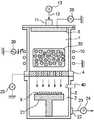
図1は、本発明の第1の実施形態におけるエッチング装置の全体構成を示す図である。図1に示すように、エッチング装置は、中性粒子ビームを生成するビーム生成室1と、半導体基板、ガラス、有機物、セラミックなどの被処理物Xが配置される処理室2とを有する円筒状の真空チャンバ3を備えている。この真空チャンバ3は、ビーム生成室1側が石英ガラス又はセラミックなどにより構成され、処理室2側が金属製のメタルチャンバなどにより構成されている。
【0019】
ビーム生成室1の外周には誘導結合型のコイル10が配置されている。このコイル10は、例えば水冷パイプのコイルであり、8mmφ程度の外径を有するコイルが2ターン程度ビーム生成室1に巻回されている。このコイル10は高周波電源20に接続されており、例えば、13.56MHzの高周波電圧がコイル10に印加される。これらのコイル10と高周波電源20とによってプラズマ生成部が構成されている。コイル10に高周波電流を流すことでプラズマ生成室1に誘導磁界が生じ、磁界の時間変化が電界を誘導し、その電界で電子が加速されてプラズマ30が生成される。
【0020】
ビーム生成室1の上部には、ガスを導入するガス導入ポート11が設けられており、このガス導入ポート11はガス供給配管12を介してガス供給源13に接続されている。このガス供給源13からはSF6,CHF3,CF4,Cl2,Ar,O2,N2,C4F8,CF3I,C2F4などのガスが真空チャンバ3内に供給される。
【0021】
処理室2には、被処理物Xを保持する保持部21が配置されており、この保持部21の上面に被処理物Xが載置されている。処理室2にはガスを排出するためのガス排出ポート22が設けられており、このガス排出ポート22はガス排出配管23を介して真空ポンプ24に接続されている。この真空ポンプ24によって処理室2は所定の圧力に維持される。また、処理室2内には、エッチング状態を計測してエッチング終点を検出する終点検出部40が配置されている。この終点検出部40としては、例えば四重極質量分析器を用いることができ、この他にもレーザ干渉、エリプソメトリなどを利用することもできる。
【0022】
ビーム生成室1の下端には、グラファイトなどの導電体で形成されたオリフィス板(オリフィス電極)4が配置されており、このオリフィス電極4は直流電源25に接続されている。図2(a)は、オリフィス電極4の斜視図、図2(b)は部分縦断面図である。図2(a)に示すように、オリフィス電極4には多数のオリフィス4aが形成されている。典型的なオリフィス電極4は、オリフィス径1mm、オリフィス長10mm、ピッチ1.4mm間隔で多数のオリフィス4aを配列している。このように、オリフィス電極4によってビーム生成室1と処理室2とを仕切ることができるので、真空ポンプ24によって処理室2の圧力をビーム生成室1の圧力よりも低くすることが可能となる。
【0023】
また、ビーム生成室1の上端には、同様に導電体で形成された電極5が配置されている。この電極5は直流電源26に接続されている。なお、電極5は穴のない金属やシリコン、グラファイトでできた板であってもよく、あるいは板に穴を多数設けて、ガスが均一にビーム生成室1に導入されるようにしてもよい。上述した直流電源25と直流電源26とによって、オリフィス電極4と電極5との間に電圧を印加する電圧印加部が構成されている。
【0024】
次に、本実施形態におけるエッチング装置の動作について説明する。本実施形態では、一例として半導体基板のシリコン酸化膜上に形成されたPolyシリコンをエッチング(ゲートエッチング)する場合を例に説明する。
【0025】
まず、真空ポンプ24を作動させることにより、真空チャンバ3内を真空排気した後に、ガス供給源13から例えばSF6などのガスをビーム生成室1の内部に導入する。この時、例えばビーム生成室1の圧力は0.1Paで処理室2の圧力は1Paである。そして、例えば13.56MHzの高周波電圧を高周波電源20によって50μ秒間コイル10に印加する。この高周波電圧の印加によってビーム生成室1内には高周波電界が形成される。真空チャンバ3内に導入されたガスは、この高周波電界によって加速された電子により電離され、ビーム生成室1内に高密度プラズマ30が生成される。このときに形成されるプラズマ30は、主として正イオンと加熱された電子とからなるプラズマである。
【0026】
そして、高周波電源20による高周波電圧の印加を50μ秒間停止する。すると電子は非弾性衝突を経て電子温度が低下し、残留している処理ガスに付着して負イオンを生成する。高周波電源20による高周波電圧の印加の停止後は、再び高周波電源20による50μ秒間の高周波電圧の印加によってビーム生成室1内においてプラズマ中の電子が加熱され、上述したサイクルが繰り返される。即ち、高周波電圧の印加(50μ秒間)と印加の停止(50μ秒間)を交互に繰り返す。この高周波電圧の印加停止時間(50μ秒間)は、プラズマ30中の電子が、残留している処理ガスに付着して、負イオンが生成されるのに要する時間よりも十分に長く、且つプラズマ30中の電子密度が低下してプラズマが消滅するよりも十分に短い時間であり、高周波電圧の印加時間(50μ秒間)は、この高周波電圧の印加を停止している間に低下したプラズマ30中の電子のエネルギーを回復させるのに十分な時間である。
【0027】
即ち、通常のプラズマは正イオンと電子とからなる場合が多いが、正イオンと共に負イオンが共存した状態のプラズマを効率的に形成することができる。なお、ここでは、高周波電圧の印加停止時間を50μ秒に設定する例について述べたが、50μ秒乃至100μ秒に設定することで、プラズマ中に正イオンのみならず負イオンを多量に生成することができる。
【0028】
ここで、直流電源25により−50Vの電圧をオリフィス板4に印加すると共に、直流電源26により−100Vの電圧を電極5に印加する。これによって、オリフィス電極4と電極5との間に電位差が生じる。従って、ビーム生成室1内の負イオン6(図2(b)参照)は、この電位差によってオリフィス電極4に向けて加速され、オリフィス電極4に形成されたオリフィス4aに入っていく。このとき、オリフィス電極4のオリフィス4aの内部を通過する負イオンは、主として、オリフィス4aの周壁の固体表面近傍において中性化され、あるいは、オリフィス4aの内部に残留しているガスとの電荷交換によって中性化され、中性粒子(フッ素原子)ビーム7となる。
【0029】
ここで、上述したオリフィス電極を用いることによって、イオンを中性化することができるだけではなく、中性粒子ビームをコリメートすることができ、更にビーム生成室1と処理室2とを仕切ることが可能となる。中性粒子ビームをコリメートすることで、高精度の加工を実現することができる。また、ビーム生成室1と処理室2とを仕切ることで、処理室2の圧力をビーム生成室1の圧力よりも低圧にして高精度の加工を実現することができる。また、プラズマから発生する放射光が被処理物に照射されるのを防止することもできる。即ち、プラズマが生成されるビーム生成室1と被処理物Xとはオリフィス電極4によって遮断されているので、プラズマから発生する放射光は被処理物Xに照射されず、被処理物Xに損傷を与えるような紫外線などの被処理物Xへの影響を低減することができる。
【0030】
上述のように、オリフィス4aの通過中に中性化された負イオンは、低エネルギーのエネルギービーム(フッ素原子)として処理室2の内部に放射される。このフッ素原子7は、処理室2の内部を直進して保持部21に載置された被処理物(半導体基板)Xに照射される。照射されたフッ素原子は、被処理物Xの被処理層(Polyシリコン層)60において、
Si+4F→SiF4↑
という熱的化学反応により、図3(a)に示すように、SiF4として自発的に昇華する。このようにしてマスク50で覆われていないPolyシリコン層60のエッチングが進行する。ここで、マスク50は有機物から構成されたレジストであるが、ビームのエネルギーが低いため、スパッタされることはない。
【0031】
このエッチングプロセスにおいては、終点検出部40によってエッチングの終点の検出を行っている。終点検出部40により終点(シリコン酸化膜70が露出する直前又は直後)が検出された場合には、直流電源25によりオリフィス板4に印加される電圧を−50Vから、例えば+100Vに変える。これによって、処理室2の内部に放射されるビームのエネルギーが高まるので、図3(b)に示すように、有機物で構成されたマスク50がスパッタされ、Polyシリコン層60の側壁がCHxFy系の有機膜80で覆われる。この有機膜80は、Polyシリコン層60の側壁をフッ素による侵食から保護する保護膜として機能する。なお、このときのビームのエネルギーは50eV以上200eV以下とすることが好ましい。
【0032】
一定の厚さの有機膜80をPolyシリコン層60の側壁に堆積させた後、オリフィス板4に印加される電圧を−50Vに戻す。これにより、処理室2の内部には再び反応性の高い低エネルギービームが放射されるが、Polyシリコン層60の側壁には保護膜80が堆積しているため、側壁が侵食されることなく、精度の高いエッチングを実現することが可能となる。また、本実施形態では、ClやBrよりも反応性の高いFラジカルを用いることができるため、高速なエッチングを実現することができる。
【0033】
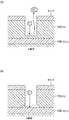
ここで、図4(a)に示すように、下地シリコン酸化膜100上に形成されたPolyシリコン層110をコリメートされた10eV以上50eV以下のフッ素の中性粒子ビームを用いてエッチング(ゲートエッチング)する場合には、上述したように、
Si+4F→SiF4↑
という反応により垂直にエッチングが進行する。エッチングが進行してシリコン酸化膜100が露出しても、シリコン酸化膜100はフッ素と反応しないため、シリコン酸化膜100はエッチングされず、Si/SiO2の選択比が高いエッチングが実現できる。しかし、図4(b)に示すように、シリコン酸化膜100上で反射したフッ素が側壁のPolyシリコン層110を侵食してしまい、形状異常が生じてしまう。本実施形態によれば、図3(b)に示すように、マスク50をスパッタしてPolyシリコン層60の側壁にフッ素による侵食から保護する保護膜80を形成することができるので、このような形状異常を防止することができる。
【0034】
本実施形態では、マスク50をスパッタしてPolyシリコン層60の側壁に保護膜80を形成した例を説明したが、グラファイト製のオリフィス電極4をスパッタしてCFxビームを生成して、上記保護膜を形成することができる。あるいは、有機物からなるメッシュ状の遮蔽板をオリフィス電極4と被処理物Xの間に挿入して、これをスパッタすることにより保護膜を形成してもよい。
【0035】
図5は、参考例としてのエッチング装置の全体構成を示す図である。図5に示すように、本参考例においては、ガス導入ポート11は、2つに分岐したガス供給配管12a,12bを介してガス供給源13a,13bに接続されている。例えば、ガス供給源13aからはSF6、ガス供給源13bからはC4F8,CHF3,C2F4などのフルオロカーボンガスが真空チャンバ3内に供給される。
【0036】
本参考例におけるエッチングプロセスでは、まず、ガス供給配管12bのバルブ15bを閉じ、ガス供給配管12aのバルブ15aを開け、SF6などのエッチングガスをビーム生成室1の内部に導入する。そして、第1の実施形態と同様にして、ビーム生成室1の内部に生成されたプラズマ30から中性粒子(フッ素原子)ビームが処理室2の内部に放射される。この低エネルギーの中性粒子ビームによって、マスクで覆われていないPolyシリコン層がエッチングされる。
【0037】
そして、終点検出部40により終点が検出された場合には、ガス供給配管12aのバルブ15aを閉じ、ガス供給配管12bのバルブ15bを開け、C4F8,CHF3,C2F4などのガスをビーム生成室1の内部に導入する。これによって、ビーム生成室1の内部に生成されたプラズマ30から正イオン(CFx+、例えばCF2+,CF+,CF3+など)が生成され、これが加速、中性化されて中性粒子ビームとして処理室2の内部に放射される。この中性粒子ビームによってPolyシリコン層の側壁がCF系の重合膜で覆われる。この重合膜は、第1の実施形態における有機膜80と同様に、Polyシリコン層の側壁をフッ素による侵食から保護する保護膜として機能する。
【0038】
一定の厚さの保護膜をPolyシリコン層の側壁に堆積させた後、再びガス供給配管12bのバルブ15bを閉じ、ガス供給配管12aのバルブ15aを開け、エッチングガスをビーム生成室1の内部に導入する。これにより、処理室2の内部には再び中性粒子(フッ素原子)ビームが放射されるが、Polyシリコン層の側壁にはCF系の側壁保護膜が堆積しているため、側壁が侵食されることなく、精度の高いエッチングを実現することが可能となる。
【0039】
上述した第1の実施形態及び参考例において、被処理層をエッチングする工程と側壁保護膜を形成する工程とを繰り返して行ってもよい。この場合には、すべての側壁保護膜がエッチング工程によって除去されるとは限らず、工程を繰り返すうちに、残った側壁保護膜によってエッチング形状がテーパ状になる場合がある。このような場合には、被処理層をエッチングする工程と側壁保護膜を形成する工程との間に、側壁保護膜を除去する工程を行うこととしてもよい。例えば、マスクにTEOS膜を用いてO2を処理室2内に導入して酸素ラジカルによって側壁保護膜を灰化することで、マスクや被処理層をエッチングすることはなく側壁保護膜を除去することができる。
【0040】
なお、一部の荷電粒子もオリフィス電極4のオリフィス4aを通過する場合があるが、このような荷電粒子が被処理物Xに照射されることを防止するために、オリフィス電極4の下流側にディフレクタや電子トラップを設けることとしてもよい。ディフレクタは、ビーム進行方向と垂直に電圧を印加することによって荷電粒子の進行方向を変化させて、荷電粒子の被処理物Xへの照射を防止するものである。また、電子トラップは、ビーム進行方向と垂直に100ガウス程度の磁界を形成することによって電子の進行方向を変化させて、電子の被処理物Xへの照射を防止するものである。
【0041】
ガラスやセラミック材料等の絶縁物の加工に際しては、表面にチャージアップという問題が生じるが、上述したように中性化された中性粒子を照射することによりチャージアップ電圧を低く保ちながら、高精度のエッチングや成膜加工が可能となる。なお、被処理物の処理の内容に応じてガスの種類を使い分ければよく、ドライエッチングでは被処理物の違いに応じて酸素やハロゲンガスなどを使い分けることができる。
【0042】
なお、上述した実施形態においては、ICP型コイルを用いてプラズマを生成した例を説明したが、ECR(Electron Cyclotron Resonance)、ヘリコン波プラズマ用コイル、マイクロ波等を用いてプラズマを生成することとしてもよい。また、高周波の周波数領域も、13.56MHzに限られるものではなく、1MHz〜20GHzの領域を用いてもよい。オリフィス電極4や電極5に印加する電圧も上述のものに限られるものではない。
【0043】
これまで本発明の一実施形態について説明したが、本発明は上述の実施形態に限定されず、その技術的思想の範囲内において種々異なる形態にて実施されてよいことは言うまでもない。
【0044】
【発明の効果】
上述したように、本発明によれば、上記第1の工程において、電荷を持たず大きな並進運動エネルギーを持つコリメートされた第1の中性粒子ビームによって被処理層を加工することが可能となるので、チャージアップ電圧を低く保ちつつ高精度のエッチングが可能となる。また、このコリメートされた第1の中性粒子ビームが被処理層に照射されるため、被処理層の表面に側壁保護膜が形成されない場合であっても、高精度の加工を実現することができる。更に、10eV以上50eV以下の低エネルギーの中性粒子ビームでは、レジストはほとんどスパッタされないため、高選択比の加工を実現することができる。ここで、RIEにおいて低エネルギーのイオンビームを照射して被処理層の加工を行った場合には、局所的なエッチング形状の異常であるノッチングが生じることがあるが、中性粒子ビームを用いるため、ノッチングの問題が生じることなく、高アスペクト比の加工を行うことが可能となる。
【0045】
また、上記第2の工程において、被処理層の側壁を第1の中性粒子ビームによる侵食から保護する保護膜を、コリメートされた第2の中性粒子ビームにより被処理層の側壁に形成することができるので、側壁の侵食を防止して精度の高いエッチングを実現することが可能となる。これは特に中性粒子ビームではエッチングされない下地層が露出した場合に有効である。また、反応性の高いエッチングガスを用いてエッチングをすることができるため、高速なエッチングを実現することができる。このように、本発明によれば、微細パターンに対して高精度の加工と高選択比の加工とを両立することが可能となる。
【図面の簡単な説明】
【図1】本発明の第1の実施形態におけるエッチング装置の全体構成を示す図である。
【図2】図1に示すオリフィス電極を示す図である。
【図3】本発明の第1の実施形態におけるエッチング工程を示す模式図である。
【図4】従来のエッチング工程を示す模式図である。
【図5】参考例としてのエッチング装置の全体構成を示す図である。
【符号の説明】
X 被処理物
1 ビーム生成室
2 処理室
3 真空チャンバ
4 オリフィス板(オリフィス電極)
5 電極
10 コイル
11 ガス導入ポート
12 ガス供給配管
13 ガス供給源
20 高周波電源
21 保持部
22 ガス排出ポート
23 ガス排出配管
24 真空ポンプ
25,26 直流電源
30 プラズマ
40 終点検出部
50 マスク
60 Polyシリコン層
70 シリコン酸化膜
80 保護膜[0001]
BACKGROUND OF THE INVENTION
The present invention relatesto a suitable etchingmethods from fine processing such as the manufacture of semiconductor devices, in particular for processing an object to be processed using a neutral beam of positive ions or negative ions generated in the plasma and neutralized it relatesto the etchinghow.
[0002]
[Prior art]
In recent years, in the fields of semiconductor integrated circuits and micromachines, the processing pattern has been remarkably miniaturized, and processing with high accuracy and high selectivity is required. In addition, high aspect ratio processing is required. In processing in this field, an etching apparatus using plasma is widely used.
[0003]
As an etching apparatus using such plasma, an RIE apparatus (reactive ion etching apparatus) that generates positive ions, radical particles, and the like is known. By irradiating the object to be processed with such positive ions or radical particles, the object to be processed can be etched.
[0004]
[Problems to be solved by the invention]
The biggest problems in the etching process using the RIE apparatus are an inability to achieve both high accuracy and a high selection ratio and an abnormal etching shape due to charge-up. Here, the selection ratio refers to a ratio of an etching depth of a workpiece to a mask or a base material in etching. That is, when the workpiece is cut by x (μm), when the mask protecting the workpiece is cut by y (μm), the selection ratio s is:
s = x / y
It is represented by The higher the selection ratio, the less the mask is damaged, so that high aspect ratio etching is possible. However, in general, in order to increase the selectivity, the gas is deposited on the surface of the mask or the underlying material, but the workpiece is selected with a gas combination that etches, and the radical is also deposited on the side wall of the workpiece. A sidewall protective film is also formed. If the side wall protective film is formed excessively, the processed cross-sectional shape becomes tapered, and the dimensional accuracy is deteriorated. The selection ratio of Si / SiO2 when O2 is added to Cl2 as a gas is about 100 at most, which is a high combination compared with other materials, but 300 or more in a device of 0.1 μm or less. High selectivity and high accuracy are demanded. In particular, achieving a high selectivity with respect to the underlying gate oxide film and no residue at the element isolation step portion is a future problem.
[0005]
Etching shape abnormality is caused by the difference in behavior between electrons and positive ions. That is, the notching occurs inside the fine line and the line facing the outer surface of the space pattern stripe. When etching with low-energy ions, inside the fine pattern, electrons are decelerated by the negative self-bias potential of the substrate and trapped near the resist, but the ions are accelerated to reach the underlying oxide film and are positively charged. Up. On the other hand, the outer periphery is neutralized because equal amounts of electrons and ions enter. For this reason, a potential difference is generated between the inside and the outside of the fine pattern, and the trajectory of ions is bent, so that notching occurs.
[0006]
The present invention has been made in view of such problems of the prior art, and provides high-precision processing for a fine pattern, a mask, and an underlayer without causing charge-up or etching shape abnormality to the object to be processed. and to providean etchinghow that can achieve both machining of high selectivity to.
[0007]
[Means for Solving the Problems]
In order to solve such a problem in the prior art, one embodiment of the present invention includes a gas supply source that supplies a gas into a vacuum chamber, a holding unit that holds an object to be processed, and a plasma in the vacuum chamber. A first electrode having an orifice and disposed upstream of the first electrode in the vacuum chamber, the first electrode having an orifice disposed between the object to be processed and the plasma generating unit By applying a voltage between the formed second electrode, and between the first electrode and the second electrode, ions are accelerated from the plasma generated by the plasma generation unit, and the first electrode An etching method using an etching apparatus provided with a voltage applying unit that passes through the orifice formed in the substrate, wherein an object to be processed having a layer to be processed locally covered by a mask made of an organic substance. Serial is held by the holding portion, thenegative ions by accelerating thenegative ions from the plasma generated from the gas passing said orifice neutralized, generating a first neutral beam collimated A first step of irradiating the object to be treated with the first neutral particle beam to etch the surface of the layer to be treated; and accelerating ions from the plasma generated from the gas and passing through the orifice The ions are neutralized to generate a collimated second neutral particle beam, and the mask is sputtered by the second neutral particle beam, whereby a protective film is formed on the sidewall of the processing target layer. The first neutral particle beam has an energy of 10 eV or more and 50 eV or less, and the second neutral particle beam has an energy of 50 eV or more and 200 eV or less. An etching method characterized by having over.
[0008]
According to the present invention, in the first step, the layer to be processed is etched bythe first neutral particle beam having no translation and having a translational kinetic energy of 10 eV or more and 50 eV or less. Electrons are not emitted and etching with a low charge-up voltage is possible. In addition, since the collimatedfirst neutral particle beam is irradiated onto the processing layer, high-precision etching can be realized even when the side wall protective film is not formed on the processing side wall of the processing layer. Can do. Specifically, in a neutral particle beam with a low energy of 10 eV or more and 50 eV or less, the layer to be treated is hardly sputtered, and etching causes a thermal chemical reaction between the neutral particle beam and the layer to be treated, resulting in a reaction product. Proceeds by spontaneous sublimation. If the neutral particles have no directionality and are in thermal motion, the processed shape becomes isotropic, but anisotropic etching can be realized because of the collimated beam. Furthermore, with a neutral particle beam with a low energy of 10 eV or more and 50 eV or less, the resist is hardly sputtered, so that processing with a high selectivity can be realized. Here, when processing a layer to be processed by irradiating a low-energy ion beam in RIE, the ion beam is bent by an electric field due to charge imbalance between ions and electrons inside the fine pattern and is locally Notching, which is an abnormal etching shape, may occur. However, since a neutral particle beam is used, high aspect ratio processing can be performed without causing a notching problem.
[0009]
In the second step, a protective film for protecting the sidewall ofthe layer to be treated from erosion bythe first neutral particle beam is formed on the sidewall of the layerto be treatedby the collimated second neutral particle beam. Therefore, it is possible to realize etching with higher accuracy by preventing erosion of the side wall. Further, since etching can be performed using a highly reactive etching gas, high-speed etching can be realized. Thus, according to the present invention, it is possible to achieve both high-precision processing and high-selectivity processing for a fine pattern.
[0011]
Another aspect of the present invention includes a gas supply source that supplies gas into a vacuum chamber, a holding unit that holds an object to be processed, a plasma generation unit that generates plasma in the vacuum chamber, and the object to be processed A first electrode having an orifice, a second electrode disposed upstream of the first electrode in the vacuum chamber, and the first electrode A voltage application unit that accelerates ions from the plasma generated by the plasma generation unit to pass through the orifice formed in the first electrode by applying a voltage between the electrode and the second electrode And an etching apparatus using an etching apparatus provided with a mesh-shaped shielding plate made of an organic substance, which is disposed between the object to be processed and the first electrode, the object to be processed having a layer to be processed The holding part The negative ions are accelerated from the plasma generated from the gas and passed through the orifice to neutralize the negative ions to generate a collimated first neutral particle beam; Irradiating the object to be processed with a neutral particle beam to etch the surface of the layer to be processed, and accelerating ions from the plasma generated from the gas to pass through the orifice. Ions are neutralized to generate a collimated second neutral particle beam, and the shielding plate is sputtered by the second neutral particle beam to form a protective film on the sidewall of the layer to be processed. The first neutral particle beam has an energy of 10 eV or more and 50 eV or less, and the second neutral particle beam has an energy of 50 eV or more and 200 eV or less. It is an etching method characterized by.
[0015]
Another preferable aspect of the present invention includes a third step of removing the protective film formed in the second step, and includes the first step, the third step, and the second step. It is characterized by being repeated.
[0016]
Another aspect of the present invention includes a gas supply source that supplies gas into a vacuum chamber, a holding unit that holds an object to be processed, a plasma generation unit that generates plasma in the vacuum chamber, and the object to be processed And a first electrode made of graphite having an orifice, a second electrode arranged upstream of the first electrode in the vacuum chamber, and the plasma generator By applying a voltage between the first electrode and the second electrode, ions are accelerated from the plasma generated by the plasma generation unit and passed through the orifice formed in the first electrode. An etching method using an etching apparatus including a voltage application unit, wherein an object to be processed having a layer to be processed is held in the holding unit, and 10 eV or more and 50 eV or less from plasma generated from the gas. And neutralized thenegative ions by passing said orifice acceleratingnegative ions at energy to produce a collimated neutral particle beam is irradiated with neutral particle beam to said object to be processed A first step of etching the surface of the layer to be treated;
Ions are accelerated from plasma generated from the gas with an energy of 50 eV or more and 200 eV or less, and the first electrode is sputtered with the accelerated ions to form a protective film on the sidewall of the layer to be processed. And an etching method characterized by comprising:
[0017]
DETAILED DESCRIPTION OF THE INVENTION
Embodiments of an etching apparatus according to the present invention will be described below in detail with reference to the drawings. 1 to 5, the same or corresponding components are denoted by the same reference numerals, and redundant description is omitted.
[0018]
FIG. 1 is a diagram showing an overall configuration of an etching apparatus according to the first embodiment of the present invention. As shown in FIG. 1, the etching apparatus has a cylindrical shape having a
[0019]
An inductively coupled
[0020]
A
[0021]
In the
[0022]
An orifice plate (orifice electrode) 4 made of a conductor such as graphite is disposed at the lower end of the
[0023]
Similarly, an
[0024]
Next, the operation of the etching apparatus in this embodiment will be described. In the present embodiment, as an example, a case where polysilicon formed on a silicon oxide film of a semiconductor substrate is etched (gate etching) will be described.
[0025]
First, by evacuating the inside of the
[0026]
Then, the application of the high frequency voltage by the high
[0027]
That is, normal plasma often consists of positive ions and electrons, but plasma in a state where negative ions coexist with positive ions can be efficiently formed. Although an example in which the high-frequency voltage application stop time is set to 50 μsec has been described here, a large amount of negative ions as well as positive ions can be generated in the plasma by setting it to 50 μsec to 100 μsec. Can do.
[0028]
Here, a voltage of −50 V is applied to the
[0029]
Here, by using the orifice electrode described above, not only can the ions be neutralized, but also the neutral particle beam can be collimated, and the
[0030]
As described above, the negative ions neutralized while passing through the
Si + 4F → SiF4 ↑
As a result of the thermal chemical reaction, as shown in FIG. 3A, it spontaneously sublimates as SiF4 . In this way, etching of the
[0031]
In this etching process, the end
[0032]
After the
[0033]
Here, as shown in FIG. 4A, the
Si + 4F → SiF4 ↑
Etching proceeds vertically by this reaction. Even if the etching progresses and the
[0034]
In the present embodiment, a description has been given of an example of forming the
[0035]
FIG. 5 is a diagram showing an overall configuration of an etching apparatusas a reference example . As shown in FIG. 5, in thisreference example , the
[0036]
In the etching process in thisreference example , first, the
[0037]
When the end point is detected by the end
[0038]
After depositing a protective film of a certain thickness on the side wall of the poly silicon layer, the
[0039]
In the first embodimentand the reference example described above, the step of etching the layer to be processed and the step of forming the sidewall protective film may be repeated. In this case, not all of the sidewall protective film is removed by the etching process, and the etching shape may become tapered due to the remaining sidewall protective film as the process is repeated. In such a case, a step of removing the sidewall protective film may be performed between the step of etching the processing target layer and the step of forming the sidewall protective film. For example, by introducing O2 into the
[0040]
Although some charged particles may also pass through the
[0041]
When processing insulators such as glass and ceramic materials, there is a problem of charge-up on the surface, but high precision is achieved while keeping the charge-up voltage low by irradiating neutral particles neutralized as described above. Etching and film formation processing are possible. Note that the type of gas may be properly used according to the processing content of the object to be processed. In dry etching, oxygen, halogen gas, or the like can be properly used according to the difference in object to be processed.
[0042]
In the above-described embodiment, an example in which plasma is generated using an ICP type coil has been described. However, plasma generation is performed using an ECR (Electron Cyclotron Resonance), a helicon wave plasma coil, a microwave, or the like. Also good. Also, the frequency region of the high frequency is not limited to 13.56 MHz, and a region of 1 MHz to 20 GHz may be used. The voltages applied to the
[0043]
Although one embodiment of the present invention has been described so far, it is needless to say that the present invention is not limited to the above-described embodiment, and may be implemented in various forms within the scope of the technical idea.
[0044]
【The invention's effect】
As described above, according to the present invention, in the first step, the layer to be processed can be processed by the collimatedfirst neutral particle beam having no charge and large translational kinetic energy. Therefore, highly accurate etching can be performed while keeping the charge-up voltage low. In addition, since the collimatedfirst neutral particle beam is irradiated to the layer to be processed, high-precision processing can be realized even when the sidewall protective film is not formed on the surface of the layer to be processed. it can. Furthermore, with a neutral particle beam with a low energy of 10 eV or more and 50 eV or less, the resist is hardly sputtered, so that processing with a high selectivity can be realized. Here, in the case of processing the layer to be processed by irradiating a low energy ion beam in RIE, a notching which is a local abnormal etching shape may occur, but a neutral particle beam is used. Thus, it becomes possible to perform high aspect ratio processing without causing notching problems.
[0045]
In the second step, a protective film for protecting the sidewall ofthe layer to be treated from erosion bythe first neutral particle beam is formed on the sidewall of the layerto be treatedby the collimated second neutral particle beam. Therefore, it is possible to prevent etching of the side wall and realize highly accurate etching. This is particularly effective when an underlying layer that is not etched by a neutral particle beam is exposed. Further, since etching can be performed using a highly reactive etching gas, high-speed etching can be realized. Thus, according to the present invention, it is possible to achieve both high-precision processing and high-selectivity processing for a fine pattern.
[Brief description of the drawings]
FIG. 1 is a diagram showing an overall configuration of an etching apparatus according to a first embodiment of the present invention.
FIG. 2 is a view showing an orifice electrode shown in FIG. 1;
FIG. 3 is a schematic diagram showing an etching process in the first embodiment of the present invention.
FIG. 4 is a schematic diagram showing a conventional etching process.
FIG. 5 is a diagram showing an overall configuration of an etching apparatusas a reference example .
[Explanation of symbols]
5
Claims (3)
Translated fromJapanese被処理物を保持する保持部と、
前記真空チャンバ内にプラズマを生成するプラズマ生成部と、
前記被処理物と前記プラズマ生成部との間に配置され、オリフィスを有する第1の電極と、
前記真空チャンバ内に前記第1の電極に対して上流側に配置された第2の電極と、
前記第1の電極と前記第2の電極との間に電圧を印加することで、前記プラズマ生成部により生成されたプラズマからイオンを加速して前記第1の電極に形成された前記オリフィスを通過させる電圧印加部とを備えたエッチング装置を用いるエッチング方法であって、
有機物から構成されたマスクにより局所的に覆われた被処理層を有する被処理物を前記保持部に保持させ、
前記ガスから生成されたプラズマから負イオンを加速して前記オリフィスを通過させることで該負イオンを中性化して、コリメートされた第1の中性粒子ビームを生成し、該第1の中性粒子ビームを前記被処理物に照射して前記被処理層の表面をエッチングする第1の工程と、
前記ガスから生成されたプラズマからイオンを加速して前記オリフィスを通過させることで該イオンを中性化して、コリメートされた第2の中性粒子ビームを生成し、該第2の中性粒子ビームによって前記マスクをスパッタすることで前記被処理層の側壁に保護膜を形成する第2の工程とを有し、
前記第1の中性粒子ビームは10eV以上50eV以下のエネルギーを有し、
前記第2の中性粒子ビームは50eV以上200eV以下のエネルギーを有することを特徴とするエッチング方法。A gas supply source for supplying gas into the vacuum chamber;
A holding unit for holding a workpiece;
A plasma generator for generating plasma in the vacuum chamber;
A first electrode disposed between the workpiece and the plasma generating unit and having an orifice;
A second electrode disposed upstream of the first electrode in the vacuum chamber;
By applying a voltage between the first electrode and the second electrode, ions are accelerated from the plasma generated by the plasma generator and pass through the orifice formed in the first electrode. An etching method using an etching apparatus including a voltage application unit to be
Holding the object to be processed having a layer to be processed locally covered by a mask made of organic matter in the holding unit;
And neutralized thenegative ions by accelerating thenegative ions from the plasma generated from the gas passing the orifice, to generate a first neutral particle beam collimated, the first neutral A first step of irradiating the object to be processed with a particle beam to etch the surface of the layer to be processed;
Ions are accelerated from the plasma generated from the gas and passed through the orifice to neutralize the ions to generate a collimated second neutral particle beam, the second neutral particle beam And a second step of forming a protective film on the sidewall of the layer to be processed by sputtering the mask.
The first neutral beam has an energy of 10 eV or more and 50 eV or less;
The etching method, wherein the second neutral particle beam has an energy of 50 eV or more and 200 eV or less.
被処理物を保持する保持部と、
前記真空チャンバ内にプラズマを生成するプラズマ生成部と、
前記被処理物と前記プラズマ生成部との間に配置され、オリフィスを有する第1の電極と、
前記真空チャンバ内に前記第1の電極に対して上流側に配置された第2の電極と、
前記第1の電極と前記第2の電極との間に電圧を印加することで、前記プラズマ生成部により生成されたプラズマからイオンを加速して前記第1の電極に形成された前記オリフィスを通過させる電圧印加部と、
前記被処理物と前記第1の電極との間に配置された、有機物からなるメッシュ状の遮蔽板とを備えたエッチング装置を用いるエッチング方法であって、
被処理層を有する被処理物を前記保持部に保持させ、
前記ガスから生成されたプラズマから負イオンを加速して前記オリフィスを通過させることで該負イオンを中性化して、コリメートされた第1の中性粒子ビームを生成し、該第1の中性粒子ビームを前記被処理物に照射して前記被処理層の表面をエッチングする第1の工程と、
前記ガスから生成されたプラズマからイオンを加速して前記オリフィスを通過させることで該イオンを中性化して、コリメートされた第2の中性粒子ビームを生成し、該第2の中性粒子ビームによって前記遮蔽板をスパッタすることで前記被処理層の側壁に保護膜を形成する第2の工程とを有し、
前記第1の中性粒子ビームは10eV以上50eV以下のエネルギーを有し、
前記第2の中性粒子ビームは50eV以上200eV以下のエネルギーを有することを特徴とするエッチング方法。A gas supply source for supplying gas into the vacuum chamber;
A holding unit for holding a workpiece;
A plasma generator for generating plasma in the vacuum chamber;
A first electrode disposed between the workpiece and the plasma generating unit and having an orifice;
A second electrode disposed upstream of the first electrode in the vacuum chamber;
By applying a voltage between the first electrode and the second electrode, ions are accelerated from the plasma generated by the plasma generator and pass through the orifice formed in the first electrode. A voltage applying unit to be
An etching method using an etching apparatus provided with a mesh-shaped shielding plate made of an organic substance, disposed between the object to be processed and the first electrode,
Hold the object to be processed having the layer to be processed in the holding part,
And neutralized thenegative ions by accelerating thenegative ions from the plasma generated from the gas passing the orifice, to generate a first neutral particle beam collimated, the first neutral A first step of irradiating the object to be processed with a particle beam to etch the surface of the layer to be processed;
Ions are accelerated from the plasma generated from the gas and passed through the orifice to neutralize the ions to generate a collimated second neutral particle beam, the second neutral particle beam And a second step of forming a protective film on the side wall of the layer to be processed by sputtering the shielding plate,
The first neutral beam has an energy of 10 eV or more and 50 eV or less;
The etching method, wherein the second neutral particle beam has an energy of 50 eV or more and 200 eV or less.
被処理物を保持する保持部と、
前記真空チャンバ内にプラズマを生成するプラズマ生成部と、
前記被処理物と前記プラズマ生成部との間に配置され、オリフィスを有するグラファイト製の第1の電極と、
前記真空チャンバ内に前記第1の電極に対して上流側に配置された第2の電極と、
前記第1の電極と前記第2の電極との間に電圧を印加することで、前記プラズマ生成部により生成されたプラズマからイオンを加速して前記第1の電極に形成された前記オリフィスを通過させる電圧印加部とを備えたエッチング装置を用いるエッチング方法であって、
被処理層を有する被処理物を前記保持部に保持させ、
前記ガスから生成されたプラズマから10eV以上50eV以下のエネルギーで負イオンを加速して前記オリフィスを通過させることで該負イオンを中性化して、コリメートされた中性粒子ビームを生成し、該中性粒子ビームを前記被処理物に照射して前記被処理層の表面をエッチングする第1の工程と、
前記ガスから生成されたプラズマから50eV以上200eV以下のエネルギーでイオンを加速し、該加速されたイオンで前記第1の電極をスパッタすることで前記被処理層の側壁に保護膜を形成する第2の工程とを有することを特徴とするエッチング方法。A gas supply source for supplying gas into the vacuum chamber;
A holding unit for holding a workpiece;
A plasma generator for generating plasma in the vacuum chamber;
A first electrode made of graphite disposed between the workpiece and the plasma generating unit and having an orifice;
A second electrode disposed upstream of the first electrode in the vacuum chamber;
By applying a voltage between the first electrode and the second electrode, ions are accelerated from the plasma generated by the plasma generator and pass through the orifice formed in the first electrode. An etching method using an etching apparatus including a voltage application unit to be
Hold the object to be processed having the layer to be processed in the holding part,
And neutralized thenegative ions by passing the orifice to acceleratenegative ions from a plasma generated from the gas at 50eV less energy than 10 eV, to produce a collimated neutral particle beam, intermediate A first step of etching the surface of the layer to be processed by irradiating the object to be processed with an active particle beam;
Ions are accelerated from plasma generated from the gas with an energy of 50 eV or more and 200 eV or less, and the first electrode is sputtered with the accelerated ions to form a protective film on the sidewall of the layer to be processed. And an etching method comprising the steps of:
Priority Applications (4)
| Application Number | Priority Date | Filing Date | Title |
|---|---|---|---|
| JP2001353809AJP4073204B2 (en) | 2001-11-19 | 2001-11-19 | Etching method |
| PCT/JP2002/011658WO2003044842A1 (en) | 2001-11-19 | 2002-11-08 | Etching method and apparatus |
| US10/493,414US7144520B2 (en) | 2001-11-19 | 2002-11-08 | Etching method and apparatus |
| TW091133466ATW589681B (en) | 2001-11-19 | 2002-11-15 | Etching method and apparatus |
Applications Claiming Priority (1)
| Application Number | Priority Date | Filing Date | Title |
|---|---|---|---|
| JP2001353809AJP4073204B2 (en) | 2001-11-19 | 2001-11-19 | Etching method |
Publications (3)
| Publication Number | Publication Date |
|---|---|
| JP2003158099A JP2003158099A (en) | 2003-05-30 |
| JP2003158099A5 JP2003158099A5 (en) | 2005-04-07 |
| JP4073204B2true JP4073204B2 (en) | 2008-04-09 |
Family
ID=19165758
Family Applications (1)
| Application Number | Title | Priority Date | Filing Date |
|---|---|---|---|
| JP2001353809AExpired - LifetimeJP4073204B2 (en) | 2001-11-19 | 2001-11-19 | Etching method |
Country Status (4)
| Country | Link |
|---|---|
| US (1) | US7144520B2 (en) |
| JP (1) | JP4073204B2 (en) |
| TW (1) | TW589681B (en) |
| WO (1) | WO2003044842A1 (en) |
Families Citing this family (30)
| Publication number | Priority date | Publication date | Assignee | Title |
|---|---|---|---|---|
| DE10317027A1 (en)* | 2003-04-11 | 2004-11-11 | Leybold Optics Gmbh | High frequency plasma beam source and method for irradiating a surface |
| JP2006049817A (en)* | 2004-07-07 | 2006-02-16 | Showa Denko Kk | Plasma processing method and plasma etching method |
| ATE532203T1 (en)* | 2004-08-27 | 2011-11-15 | Fei Co | LOCALIZED PLASMA TREATMENT |
| KR100851901B1 (en)* | 2005-01-07 | 2008-08-13 | 삼성전자주식회사 | Apparatus for extraction ion beam |
| KR100714898B1 (en)* | 2005-01-21 | 2007-05-04 | 삼성전자주식회사 | Substrate processing apparatus and processing method using neutral beam |
| KR100610665B1 (en) | 2005-02-03 | 2006-08-09 | 삼성전자주식회사 | Etching Device Using Neutral Beam |
| US7358484B2 (en)* | 2005-09-29 | 2008-04-15 | Tokyo Electron Limited | Hyperthermal neutral beam source and method of operating |
| US7335602B2 (en)* | 2006-01-18 | 2008-02-26 | Freescale Semiconductor, Inc. | Charge-free layer by layer etching of dielectrics |
| US20080169064A1 (en)* | 2007-01-11 | 2008-07-17 | Ushio Denki Kabushiki Kaisha | Surface-treating apparatus |
| CN101542694A (en)* | 2007-02-09 | 2009-09-23 | 佳能安内华股份有限公司 | Oxidation method and oxidation apparatus |
| US20090013527A1 (en)* | 2007-07-11 | 2009-01-15 | International Business Machines Corporation | Collapsable connection mold repair method utilizing femtosecond laser pulse lengths |
| KR100898589B1 (en)* | 2007-08-13 | 2009-05-20 | 주식회사 하이닉스반도체 | Semiconductor device manufacturing method |
| US8614151B2 (en)* | 2008-01-04 | 2013-12-24 | Micron Technology, Inc. | Method of etching a high aspect ratio contact |
| JP2010228066A (en)* | 2009-03-27 | 2010-10-14 | Kyushu Univ | Nanodot fabrication method |
| US20110177694A1 (en)* | 2010-01-15 | 2011-07-21 | Tokyo Electron Limited | Switchable Neutral Beam Source |
| US8828883B2 (en) | 2010-08-24 | 2014-09-09 | Micron Technology, Inc. | Methods and apparatuses for energetic neutral flux generation for processing a substrate |
| FR2965697B1 (en)* | 2010-09-30 | 2014-01-03 | Astrium Sas | METHOD AND DEVICE FOR FORMING A PLASMA BEAM. |
| US9070760B2 (en)* | 2011-03-14 | 2015-06-30 | Plasma-Therm Llc | Method and apparatus for plasma dicing a semi-conductor wafer |
| CN102332384A (en)* | 2011-09-26 | 2012-01-25 | 中国科学院微电子研究所 | Apparatus and method for generating neutral particle beams |
| US9048190B2 (en)* | 2012-10-09 | 2015-06-02 | Applied Materials, Inc. | Methods and apparatus for processing substrates using an ion shield |
| KR101742556B1 (en) | 2012-11-02 | 2017-06-01 | 캐논 아네르바 가부시키가이샤 | Method for manufacturing semiconductor device, ion beam etching device, and control device |
| US9978568B2 (en) | 2013-08-12 | 2018-05-22 | Tokyo Electron Limited | Self-sustained non-ambipolar direct current (DC) plasma at low power |
| KR101579506B1 (en)* | 2014-07-08 | 2015-12-23 | 피에스케이 주식회사 | Apparatus for treating substrate and method for handling particles thereof |
| US20160013020A1 (en)* | 2014-07-14 | 2016-01-14 | Lam Research Corporation | Systems and methods for producing energetic neutrals |
| US10475626B2 (en) | 2015-03-17 | 2019-11-12 | Applied Materials, Inc. | Ion-ion plasma atomic layer etch process and reactor |
| US9960089B2 (en)* | 2015-04-03 | 2018-05-01 | Varian Semiconductor Equipment Associates, Inc. | Apparatus and method for endpoint detection |
| DE102016220248A1 (en)* | 2016-10-17 | 2018-04-19 | Fraunhofer-Gesellschaft zur Förderung der angewandten Forschung e.V. | APPARATUS AND METHOD FOR ANISOTROPIC DRY EQUIPMENT FLUORESCENT MIXING |
| JP6790731B2 (en)* | 2016-11-01 | 2020-11-25 | 東洋製罐グループホールディングス株式会社 | Method of forming microperiodic structure grooves on the surface of diamond film |
| CN107331593B (en)* | 2017-08-11 | 2018-10-12 | 大连理工大学 | A kind of negative ions source based on radio frequency discharge |
| JP7323476B2 (en)* | 2020-02-19 | 2023-08-08 | 住友電気工業株式会社 | Semiconductor device manufacturing method |
Family Cites Families (8)
| Publication number | Priority date | Publication date | Assignee | Title |
|---|---|---|---|---|
| US4523971A (en)* | 1984-06-28 | 1985-06-18 | International Business Machines Corporation | Programmable ion beam patterning system |
| DE4039930A1 (en)* | 1990-12-14 | 1992-06-17 | Leybold Ag | Plasma treating appts. - has adjustable distance between edge of hollow electrode and substrate holding electrode to maintain constant radio frequency power |
| JPH0775230B2 (en)* | 1991-09-24 | 1995-08-09 | 株式会社小電力高速通信研究所 | Plasma etching end point monitoring method |
| US5462629A (en)* | 1992-08-28 | 1995-10-31 | Kawasaki Steel Corp. | Surface processing apparatus using neutral beam |
| DE4241045C1 (en)* | 1992-12-05 | 1994-05-26 | Bosch Gmbh Robert | Process for anisotropic etching of silicon |
| US6054395A (en)* | 1997-10-24 | 2000-04-25 | Micron Technology, Inc. | Method of patterning a semiconductor device |
| US6641747B1 (en)* | 2001-02-15 | 2003-11-04 | Advanced Micro Devices, Inc. | Method and apparatus for determining an etch endpoint |
| JP4039834B2 (en)* | 2001-09-28 | 2008-01-30 | 株式会社荏原製作所 | Etching method and etching apparatus |
- 2001
- 2001-11-19JPJP2001353809Apatent/JP4073204B2/ennot_activeExpired - Lifetime
- 2002
- 2002-11-08WOPCT/JP2002/011658patent/WO2003044842A1/enactiveApplication Filing
- 2002-11-08USUS10/493,414patent/US7144520B2/ennot_activeExpired - Fee Related
- 2002-11-15TWTW091133466Apatent/TW589681B/ennot_activeIP Right Cessation
Also Published As
| Publication number | Publication date |
|---|---|
| WO2003044842A1 (en) | 2003-05-30 |
| US7144520B2 (en) | 2006-12-05 |
| TW589681B (en) | 2004-06-01 |
| US20040244687A1 (en) | 2004-12-09 |
| TW200300579A (en) | 2003-06-01 |
| JP2003158099A (en) | 2003-05-30 |
Similar Documents
| Publication | Publication Date | Title |
|---|---|---|
| JP4073204B2 (en) | Etching method | |
| JP4039834B2 (en) | Etching method and etching apparatus | |
| US6136387A (en) | Ion flow forming method and apparatus | |
| US4609428A (en) | Method and apparatus for microwave plasma anisotropic dry etching | |
| US5593539A (en) | Plasma source for etching | |
| JP3912993B2 (en) | Neutral particle beam processing equipment | |
| KR970000419B1 (en) | Plasma Generator | |
| US6926799B2 (en) | Etching apparatus using neutral beam | |
| KR970005035B1 (en) | Method and apparatus for generating highly dense uniform plasma by use of a high frequency rotating electric field | |
| US6909087B2 (en) | Method of processing a surface of a workpiece | |
| JP2003158099A5 (en) | ||
| JP4042817B2 (en) | Neutral particle beam processing equipment | |
| JP2002289582A (en) | Neutral particle beam treatment device | |
| CN118280830A (en) | Etching method and etching system | |
| JPH05102083A (en) | Dry etching method and apparatus therefor | |
| Darnon | Plasma etching in microelectronics | |
| Ono et al. | RF-plasma-assisted fast atom beam etching | |
| JP2851765B2 (en) | Plasma generation method and apparatus | |
| CN118280829A (en) | Etching method and etching system | |
| JPH0458176B2 (en) | ||
| JPH0770510B2 (en) | Plasma processing device | |
| JP2006253190A (en) | Neutral particle beam processing apparatus and method of neutralizing charge | |
| JPH08203869A (en) | Method and system for plasma processing | |
| JPH0794485A (en) | Surface treatment method and apparatus | |
| JPH05121366A (en) | Dry etching method |
Legal Events
| Date | Code | Title | Description |
|---|---|---|---|
| A521 | Written amendment | Free format text:JAPANESE INTERMEDIATE CODE: A523 Effective date:20040507 | |
| A621 | Written request for application examination | Free format text:JAPANESE INTERMEDIATE CODE: A621 Effective date:20040507 | |
| A711 | Notification of change in applicant | Free format text:JAPANESE INTERMEDIATE CODE: A712 Effective date:20040618 | |
| A521 | Written amendment | Free format text:JAPANESE INTERMEDIATE CODE: A523 Effective date:20040714 | |
| A521 | Written amendment | Free format text:JAPANESE INTERMEDIATE CODE: A523 Effective date:20060223 | |
| RD02 | Notification of acceptance of power of attorney | Free format text:JAPANESE INTERMEDIATE CODE: A7422 Effective date:20060223 | |
| A521 | Written amendment | Free format text:JAPANESE INTERMEDIATE CODE: A821 Effective date:20060223 | |
| A131 | Notification of reasons for refusal | Free format text:JAPANESE INTERMEDIATE CODE: A131 Effective date:20070206 | |
| A521 | Written amendment | Free format text:JAPANESE INTERMEDIATE CODE: A523 Effective date:20070404 | |
| A131 | Notification of reasons for refusal | Free format text:JAPANESE INTERMEDIATE CODE: A131 Effective date:20070710 | |
| RD02 | Notification of acceptance of power of attorney | Free format text:JAPANESE INTERMEDIATE CODE: A7422 Effective date:20070823 | |
| A521 | Written amendment | Free format text:JAPANESE INTERMEDIATE CODE: A523 Effective date:20070905 | |
| A131 | Notification of reasons for refusal | Free format text:JAPANESE INTERMEDIATE CODE: A131 Effective date:20071106 | |
| A521 | Written amendment | Free format text:JAPANESE INTERMEDIATE CODE: A523 Effective date:20071219 | |
| TRDD | Decision of grant or rejection written | ||
| A01 | Written decision to grant a patent or to grant a registration (utility model) | Free format text:JAPANESE INTERMEDIATE CODE: A01 Effective date:20080122 | |
| A61 | First payment of annual fees (during grant procedure) | Free format text:JAPANESE INTERMEDIATE CODE: A61 Effective date:20080122 | |
| FPAY | Renewal fee payment (event date is renewal date of database) | Free format text:PAYMENT UNTIL: 20110201 Year of fee payment:3 | |
| R150 | Certificate of patent or registration of utility model | Free format text:JAPANESE INTERMEDIATE CODE: R150 Ref document number:4073204 Country of ref document:JP Free format text:JAPANESE INTERMEDIATE CODE: R150 | |
| S111 | Request for change of ownership or part of ownership | Free format text:JAPANESE INTERMEDIATE CODE: R313117 Free format text:JAPANESE INTERMEDIATE CODE: R313113 | |
| FPAY | Renewal fee payment (event date is renewal date of database) | Free format text:PAYMENT UNTIL: 20110201 Year of fee payment:3 | |
| R350 | Written notification of registration of transfer | Free format text:JAPANESE INTERMEDIATE CODE: R350 | |
| FPAY | Renewal fee payment (event date is renewal date of database) | Free format text:PAYMENT UNTIL: 20110201 Year of fee payment:3 | |
| FPAY | Renewal fee payment (event date is renewal date of database) | Free format text:PAYMENT UNTIL: 20120201 Year of fee payment:4 | |
| R250 | Receipt of annual fees | Free format text:JAPANESE INTERMEDIATE CODE: R250 | |
| FPAY | Renewal fee payment (event date is renewal date of database) | Free format text:PAYMENT UNTIL: 20120201 Year of fee payment:4 | |
| FPAY | Renewal fee payment (event date is renewal date of database) | Free format text:PAYMENT UNTIL: 20130201 Year of fee payment:5 | |
| R250 | Receipt of annual fees | Free format text:JAPANESE INTERMEDIATE CODE: R250 | |
| R250 | Receipt of annual fees | Free format text:JAPANESE INTERMEDIATE CODE: R250 | |
| R250 | Receipt of annual fees | Free format text:JAPANESE INTERMEDIATE CODE: R250 | |
| R250 | Receipt of annual fees | Free format text:JAPANESE INTERMEDIATE CODE: R250 | |
| R250 | Receipt of annual fees | Free format text:JAPANESE INTERMEDIATE CODE: R250 | |
| R250 | Receipt of annual fees | Free format text:JAPANESE INTERMEDIATE CODE: R250 | |
| R250 | Receipt of annual fees | Free format text:JAPANESE INTERMEDIATE CODE: R250 | |
| R250 | Receipt of annual fees | Free format text:JAPANESE INTERMEDIATE CODE: R250 | |
| R250 | Receipt of annual fees | Free format text:JAPANESE INTERMEDIATE CODE: R250 | |
| R250 | Receipt of annual fees | Free format text:JAPANESE INTERMEDIATE CODE: R250 | |
| EXPY | Cancellation because of completion of term |