JP4073174B2 - Neutral particle beam processing equipment - Google Patents
Neutral particle beam processing equipmentDownload PDFInfo
- Publication number
- JP4073174B2 JP4073174B2JP2001088863AJP2001088863AJP4073174B2JP 4073174 B2JP4073174 B2JP 4073174B2JP 2001088863 AJP2001088863 AJP 2001088863AJP 2001088863 AJP2001088863 AJP 2001088863AJP 4073174 B2JP4073174 B2JP 4073174B2
- Authority
- JP
- Japan
- Prior art keywords
- orifice
- plasma
- electrode
- ions
- negative ions
- Prior art date
- Legal status (The legal status is an assumption and is not a legal conclusion. Google has not performed a legal analysis and makes no representation as to the accuracy of the status listed.)
- Expired - Fee Related
Links
Images


Classifications
- H—ELECTRICITY
- H01—ELECTRIC ELEMENTS
- H01J—ELECTRIC DISCHARGE TUBES OR DISCHARGE LAMPS
- H01J37/00—Discharge tubes with provision for introducing objects or material to be exposed to the discharge, e.g. for the purpose of examination or processing thereof
- H01J37/32—Gas-filled discharge tubes
- H01J37/32009—Arrangements for generation of plasma specially adapted for examination or treatment of objects, e.g. plasma sources
- H01J37/32082—Radio frequency generated discharge
- H01J37/32137—Radio frequency generated discharge controlling of the discharge by modulation of energy
- H—ELECTRICITY
- H01—ELECTRIC ELEMENTS
- H01J—ELECTRIC DISCHARGE TUBES OR DISCHARGE LAMPS
- H01J37/00—Discharge tubes with provision for introducing objects or material to be exposed to the discharge, e.g. for the purpose of examination or processing thereof
- H01J37/02—Details
- H01J37/04—Arrangements of electrodes and associated parts for generating or controlling the discharge, e.g. electron-optical arrangement or ion-optical arrangement
- H01J37/08—Ion sources; Ion guns
- H—ELECTRICITY
- H01—ELECTRIC ELEMENTS
- H01J—ELECTRIC DISCHARGE TUBES OR DISCHARGE LAMPS
- H01J37/00—Discharge tubes with provision for introducing objects or material to be exposed to the discharge, e.g. for the purpose of examination or processing thereof
- H01J37/30—Electron-beam or ion-beam tubes for localised treatment of objects
- H—ELECTRICITY
- H01—ELECTRIC ELEMENTS
- H01J—ELECTRIC DISCHARGE TUBES OR DISCHARGE LAMPS
- H01J37/00—Discharge tubes with provision for introducing objects or material to be exposed to the discharge, e.g. for the purpose of examination or processing thereof
- H01J37/32—Gas-filled discharge tubes
- H01J37/32009—Arrangements for generation of plasma specially adapted for examination or treatment of objects, e.g. plasma sources
- H01J37/32357—Generation remote from the workpiece, e.g. down-stream
- H—ELECTRICITY
- H01—ELECTRIC ELEMENTS
- H01J—ELECTRIC DISCHARGE TUBES OR DISCHARGE LAMPS
- H01J2237/00—Discharge tubes exposing object to beam, e.g. for analysis treatment, etching, imaging
- H01J2237/06—Sources
- H01J2237/08—Ion sources
- H01J2237/0822—Multiple sources
- H01J2237/0827—Multiple sources for producing different ions sequentially
Landscapes
- Chemical & Material Sciences (AREA)
- Analytical Chemistry (AREA)
- Physics & Mathematics (AREA)
- Engineering & Computer Science (AREA)
- Plasma & Fusion (AREA)
- Plasma Technology (AREA)
- Drying Of Semiconductors (AREA)
- Physical Or Chemical Processes And Apparatus (AREA)
- Physical Vapour Deposition (AREA)
Description
Translated fromJapanese【0001】
【発明の属する技術分野】
本発明は、中性粒子ビーム処理装置、特に高密度プラズマから高指向性で且つ高密度の粒子ビームを生成し、被処理物を加工する中性粒子ビーム処理装置に関するものである。
【0002】
【従来の技術】
近年、半導体集積回路、ハードディスク等の情報記憶媒体、あるいはマイクロマシーン等の分野において、その加工パターンが著しく微細化されている。かかる分野の加工においては、直進性が高く(高指向性であり)、且つ比較的大口径で高密度のイオンビーム等のエネルギービームを照射して被処理物の成膜又はエッチングなどを施す技術が注目されている。
【0003】
このようなエネルギービームのビーム源としては、正イオン、負イオン、ラジカル粒子等の各種のビームを生成するものが知られている。このような正イオン、負イオン、ラジカル粒子等のビームをビーム源から被処理物の任意の部位に照射することで、被処理物の局所的な成膜やエッチング、表面改質、接合、接着などを行うことができる。
【0004】
【発明が解決しようとする課題】
正イオンや負イオンなどの荷電粒子を被処理物に照射するビーム源においては、被処理物に電荷が蓄積するため絶縁物を処理することができない(チャージアップ現象)。また、空間電荷効果でイオンビームが発散してしまうため微細な加工をすることができない。
【0005】
これを防ぐためにイオンビームに電子を注ぎ込むことで電荷を中和することも考えられているが、この方法では全体的な電荷のバランスは取れるものの、局所的には電荷のアンバランスが生じており、やはり微細な加工をすることができない。
【0006】
また、プラズマ源からイオンを引き出して被処理物に照射する場合において、プラズマから発生する紫外線などの放射光が被処理物に照射されると被処理物に悪影響を与えることとなるので、プラズマから放出される紫外線などの放射光を遮蔽する必要がある。
【0007】
本発明は、このような従来技術の問題点に鑑みてなされたもので、安価且つコンパクトな構成で大口径のビームを被処理物に照射することができると共に高い中性化率を得ることができ、チャージフリー且つダメージフリーな中性粒子ビーム処理装置を提供することを目的とする。
【0008】
【課題を解決するための手段】
このような従来技術における問題点を解決するために、本発明の一態様は、被処理物を保持する保持部と、高周波電圧の印加と印加の停止とを交互に繰り返すことにより、真空チャンバ内に正イオンと負イオンとを含むプラズマを生成するプラズマ生成部と、上記真空チャンバ内であって、上記プラズマ生成部と上記被処理物との間に配置され、上記プラズマから放出される紫外線を遮蔽するオリフィス電極と、上記真空チャンバ内に上記オリフィス電極に対して上流側に配置されたグリッド電極と、上記オリフィス電極と上記グリッド電極との間に400kHzの低周波電圧を印加することで、上記プラズマ生成部により生成されたプラズマから正イオンと負イオンとを交互に引き出す電圧印加部とを備え、上記電圧印加部によりプラズマから正イオンと負イオンとを交互に引き出して上記オリフィス電極に形成されたオリフィスを通過させることで、該正イオンと該負イオンを該オリフィス内で中性化させることを特徴とする中性粒子ビーム処理装置である。
【0009】
このような構成により、正イオンと負イオンとを交互に引き出し、これらを中性化して中性粒子ビームとして被処理物に照射することができる。
【0011】
本発明の他の一態様は、被処理物を保持する保持部と、真空チャンバ内に配置され、プラズマから放出される紫外線を遮蔽するオリフィス電極と、上記真空チャンバ内に上記オリフィス電極に対して上流側に配置されたグリッド電極と、上記オリフィス電極と上記グリッド電極との間に高周波電圧の印加と印加の停止とを交互に繰り返すことで、上記オリフィス電極と上記グリッド電極との間に正イオンと負イオンとを含むプラズマを生成すると共に、上記オリフィス電極と上記グリッド電極との間に400kHzの低周波電圧を印加することで上記プラズマから正イオンと負イオンとを交互に引き出す電圧印加部とを備え、上記電圧印加部によりプラズマから正イオンと負イオンとを交互に引き出して上記オリフィス電極に形成されたオリフィスを通過させることで、該正イオンと該負イオンを該オリフィス内で中性化させることを特徴とする中性粒子ビーム処理装置である。
【0012】
このような構成により、正イオンと負イオンとを交互に引き出し、これらを中性化して中性粒子ビームとして被処理物に照射することができる。特に、電圧印加部を正イオンと負イオンとをプラズマ中から引き出す手段としてだけでなく、プラズマを生成する手段としても利用することができる。従って、上記のように構成した場合には、プラズマを生成するためのプラズマ生成部を別に設ける必要がなくなる。このため、装置をよりコンパクトにして安価にビームを大口径化することが可能となる。
【0014】
また、正イオンと負イオンとを交互に引き出し、これらを中性化して電荷を持たず大きな並進運動エネルギーを持つ中性粒子線によって被処理物を加工することが可能となるので、チャージアップ量を小さく保ちつつ高精度のエッチングや成膜加工が可能となる。また、正イオンの中性化による中性粒子と負イオンの中性化による中性粒子とを交互に照射することで、2種類の処理を交互に行うことができる。例えば、真空チャンバ内に導入するガスをCl2とXeとした場合、正イオンの中性化によるXeを用いてXeスパッタを行い、負イオンの中性化による塩素を用いて塩素エッチングを行うことができるので、ケミカルスパッタリング作用でエッチレートを高めることができる。また、例えば、塩素ビームを照射して塩素と被処理物とが弱い結合力になっている数原子層を形成し、そこに、その弱い結合力の原子層は除去できるが被処理物自体の強い結合力は切ることができない程度のエネルギーを持つXeビームでスパッタリング除去するというように、適切な反応プロセスとエネルギー制御を行えば、被処理物の原子の結晶構造を破壊することなくエッチングすることが可能となる。
【0015】
上記電圧印加部は、上記オリフィス電極と上記グリッド電極との間に可変電圧を印加することで、上記プラズマから正イオンと負イオンとを交互に引き出して上記オリフィス電極に形成されたオリフィスを通過させる。このように構成すれば、上述の電圧印加部を正イオンと負イオンとをプラズマ中から引き出す手段としてだけでなく、正イオン及び負イオンを中性化する手段としても利用することができる。この場合において、中性化する手段としてオリフィス電極を用いることによって高い中性化率が得られるので、装置を大型化せずに安価にビームを大口径化することが可能となる。更に、生成されたプラズマと被処理物とはオリフィス電極によって遮断されるので、プラズマから発生する放射光は被処理物に照射されず、被処理物に損傷を与えるような紫外線などの被処理物への影響を低減することができる。
【0016】
【発明の実施の形態】
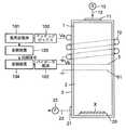
以下、本発明に係るビーム処理装置の第1の実施形態について図1乃至図3を参照して詳細に説明する。図1は、本発明の第1の実施形態におけるビーム処理装置の全体構成を示す図である。
【0017】
図1に示すように、ビーム処理装置は、中性粒子ビームを生成するビーム生成室1と半導体基板、ガラス、有機物、セラミックスなどの被処理物Xの加工を行う処理室2とを有する円筒状の真空チャンバ3を備えている。この真空チャンバ3は、ビーム生成室1側が石英ガラス又はセラミックなどにより構成され、処理室2側が金属製のメタルチャンバなどにより構成されている。
【0018】
ビーム生成室1の外周には誘導結合型のコイル10が配置されている。このコイル10は、例えば水冷パイプのコイルであり、8mmφ程度の外径を有するコイルが2ターン程度ビーム生成室1に巻回されている。このコイル10は、マッチングボックス100を介して高周波電源101に接続されており、例えば、13.56MHzの高周波電圧がコイル10に印加される。これらのコイル10、マッチングボックス100、高周波電源101によってプラズマ生成部が構成されている。即ち、コイル10に高周波電流を流すことで誘導磁場を生じさせ、その変位電流によりガス中の原子・分子が電離されプラズマが生成する。
【0019】
ビーム生成室1の上部には、真空チャンバ3内にガスを導入するガス導入ポート11が設けられており、このガス導入ポート11はガス供給配管12を介してガス供給源13に接続されている。このガス供給源13からはSF6,CHF3,CF4,Cl2,Ar,O2,N2,C4F8等などのガスが真空チャンバ3内に供給される。
【0020】
処理室2には、被処理物Xを保持する保持部20が配置されており、この保持部20の上面に被処理物Xが載置されている。処理室2にはガスを排出するためのガス排出ポート21が設けられており、このガス排出ポート21はガス排出配管22を介して真空ポンプ23に接続されている。この真空ポンプ23によって処理室2は所定の圧力に維持される。
【0021】
ビーム生成室1の下端には、グラファイトなどの導電体で形成されたオリフィス板(オリフィス電極)4が配置されており、このオリフィス電極4は接地電位とされる。このオリフィス電極4は第1の電極及び中性化手段として機能するものである。また、このオリフィス電極4の上方には、同様に導電体で形成された薄板グリッド状のグリッド電極(第2の電極)5が配置されている。このグリッド電極5はバイポーラ電源102(電圧印加部)に接続されている。このバイポーラ電源102によって例えば400kHzの低周波電圧がグリッド電極5に印加される。図2は、オリフィス電極4及びグリッド電極5の斜視図(図2(a))と部分縦断面図(図2(b))である。図2に示すように、オリフィス電極4には多数のオリフィス4aが形成されており、同様にグリッド電極5には多数のグリッド穴5aが形成されている。なお、グリッド電極5はメッシュ網やパンチングメタルなどであってもよい。
【0022】
コイル10に接続される高周波電源101とバイポーラ電源102とにはそれぞれ変調装置103、104が接続されている。高周波電源101とバイポーラ電源102とは変調装置103、104を介して互いに接続されており、変調装置103、104間の同期信号によって、高周波電源101による電圧印加のタイミングとバイポーラ電源102による電圧印加のタイミングとが同期される。
【0023】
次に、本実施形態におけるビーム処理装置の動作について説明する。図3は、本実施形態における動作状態を示すタイムチャートである。図3において、Vaはコイル10の電位、Teはビーム生成室1内の電子温度、neはビーム生成室1内の電子密度、ni−はビーム生成室1内の負イオン密度、Vbはグリッド電極5の電位をそれぞれ示している。なお、図3のタイムチャートは模式的なものであって、例えば図示されている周期は実際の周期とは異なる。
【0024】
まず、真空ポンプ23を作動させることにより、真空チャンバ3内を真空排気した後に、ガス供給源13からSF6,CHF3,CF4,Cl2,Ar,O2,N2,C4F8等などのガスを真空チャンバ3の内部に導入する。そして、図3に示すように、13.56MHzの高周波電圧を高周波電源101によって10μ秒間コイル10に印加する。この高周波電圧の印加によってビーム生成室1内には高周波電界が形成される。真空チャンバ3内に導入されたガスは、この高周波電界によって加速された電子により電離され、ビーム生成室1内に高密度プラズマが生成される。このときに形成されるプラズマは、主として正イオンと加熱された電子とからなるプラズマである。
【0025】
そして、高周波電源101による高周波電圧の印加を100μ秒間停止する。高周波電源101による高周波電圧の印加の停止後は、再び高周波電源101による10μ秒間の高周波電圧の印加によってビーム生成室1内においてプラズマ中の電子が加熱され、上述したサイクルが繰り返される。即ち、高周波電界の印加(10μ秒間)と印加の停止(100μ秒間)を交互に繰り返す。この高周波電界の印加停止時間(100μ秒間)は、プラズマ中の電子が残留している処理ガスに付着して負イオンが生成されるのに要する時間よりも十分に長く、且つプラズマ中の電子密度が低下してプラズマが消滅するよりも十分に短い時間である。高周波電界の印加時間(10μ秒間)は、この高周波電界の印加を停止している間に低下したプラズマ中の電子のエネルギーを回復させるのに十分な時間である。
【0026】
このプラズマ中の電子のエネルギーを高めた後の高周波電界の印加停止により、負イオンを効率よく且つ継続して生成することができる。即ち、通常のプラズマは正イオンと電子とからなる場合が多いが、正イオンと共に負イオンが共存した状態のプラズマを効率的に形成することができる。なお、ここでは、高周波電界の印加停止時間を100μ秒に設定する例について述べたが、50μ秒乃至100μ秒に設定することで、プラズマ中に正イオンのみならず負イオンを多量に生成することができる。
【0027】
高周波電源101による電圧の印加の停止から50μ秒後に、バイポーラ電源102によって400kHzの低周波電圧をグリッド電極5に50μ秒間印加する。この低周波電圧の印加において、グリッド電極5の電位Vbがオリフィス電極4の電位(接地電位)よりも高いとき(例えば図3のAで示す部分)には、オリフィス電極4とグリッド電極5との間に、オリフィス電極4を陰極、グリッド電極5を陽極とした電位差が生じる。従って、グリッド電極5からオリフィス電極4側に漏れ出た正イオン6(図2(b)参照)は、この電位差によってオリフィス電極4に向けて加速され、オリフィス電極4に形成されたオリフィス4aに入っていく。
【0028】
このとき、オリフィス電極4のオリフィス4aの内部を通過する正イオン6は、主として、オリフィス4aの周壁の固体表面近傍において中性化されるか、オリフィス4aの内部に残留しているガスとの電荷交換によって中性化されるか、あるいは、オリフィス電極4の表面から放出された電子と衝突して再結合することによって中性化され、中性粒子7となる。
【0029】
一方、グリッド電極5の電位Vbがオリフィス電極4の電位(接地電位)よりも低いとき(例えば図3のBで示す部分)には、オリフィス電極4とグリッド電極5との間に、オリフィス電極4を陽極、グリッド電極5を陰極とした電位差が生じる。従って、グリッド電極5からオリフィス電極4側に漏れ出た負イオンは、この電位差によってオリフィス電極4に向けて加速され、オリフィス電極4に形成されたオリフィス4aに入っていく。オリフィス電極4のオリフィス4aの内部を通過する負イオンは、主として、オリフィス4aの周壁の固体表面近傍において中性化され、あるいは、オリフィス4aの内部に残留しているガスとの電荷交換によって中性化され、中性粒子7となる。
【0030】
このようにして、オリフィス4aの通過中に中性化された正イオン又は負イオン(中性粒子)は、交互にエネルギービームとして処理室2の内部に放射される。この中性粒子7は、処理室2の内部を直進して保持部20に載置された被処理物Xに照射され、この中性粒子7によってエッチング、クリーニング、窒化処理や酸化処理などの表面改質、成膜などの処理を行うことが可能となる。
【0031】
このように正イオンの中性化による中性粒子と負イオンの中性化による中性粒子とを交互に照射することで、2種類の処理を交互に行うことができる。例えば、真空チャンバ3内に導入するガスをCl2とXeとした場合、正イオンの中性化によるXeを用いてXeスパッタを行い、負イオンの中性化による塩素を用いて塩素エッチングを行うことができるので、ケミカルスパッタリング作用でエッチレートを高めることができる。
【0032】
また、例えば、塩素ビームを照射して塩素と被処理物とが弱い結合力になっている数原子層を形成し、そこに、その弱い結合力の原子層は除去できるが被処理物自体の強い結合力は切ることができない程度のエネルギーを持つXeビームでスパッタリング除去するというように、適切な反応プロセスとエネルギー制御を行えば、被処理物の原子の結晶構造を破壊することなくエッチングすることが可能となる。
【0033】
この場合において、オリフィス電極は、イオンを中性化する手段としてだけではなく、プラズマから発生する放射光が被処理物に照射されるのを防止する手段としても機能する。即ち、プラズマが生成されるビーム生成室1と被処理物Xとはオリフィス電極4によって遮断されているので、プラズマから発生する放射光は被処理物Xに照射されず、被処理物Xに損傷を与えるような紫外線などの被処理物Xへの影響を低減することができる。
【0034】
なお、一部の荷電粒子もオリフィス電極4のオリフィス4aを通過する場合があるが、このような荷電粒子が被処理物Xに照射されることを防止するために、オリフィス電極4の下流側にディフレクタや電子トラップを設けることとしてもよい。ディフレクタは、真空チャンバ3の径方向に電圧を印加することによって荷電粒子の進行方向を変化させて、荷電粒子の被処理物Xへの照射を防止するものである。また、電子トラップは、径方向に磁界を形成することによって荷電粒子の進行方向を変化させて、荷電粒子の被処理物Xへの照射を防止するものである。
【0035】
ガラスやセラミック材料等の絶縁物の加工に際しては、表面にチャージアップという問題が生じるが、このように中性化された中性粒子を照射することによりチャージアップ量を小さく保ちながら、高精度のエッチングや成膜加工が可能となる。なお、被処理物の処理の内容に応じてガスの種類を使い分ければよく、ドライエッチングでは被処理物の違いに応じて酸素やハロゲンガスなどを使い分けることができる。
【0036】
本実施形態では、グリッド電極5をコイル10の下流側に配置した例を説明したが、グリッド電極をコイル10の上流側に配置することもできる。この場合は、グリッド電極に穴が1つも形成されていなくてもよい。図4はグリッド電極50をコイル10の上流側に配置した場合のビーム処理装置の全体構成を示す図である。この場合には、ビーム生成室1内に生成されたプラズマ中の正イオン及び負イオンはグリッド電極50とオリフィス電極4との間で加速されることとなる。
【0037】
また、本実施形態では、中性化手段としてオリフィス電極を用いた例を説明したが、これに限られず他の中性化手段を用いることもできる。例えば、▲1▼プラズマから引き出されたイオンに電子ビームを照射することで中性化する、▲2▼引き出されたイオンの経路上に中性ガスを導入して中性ガスの圧力の高い領域を形成し、この領域を通過させることでイオンを中性化する、▲3▼イオンに光を照射することで中性化する、▲4▼イオンを高周波電場で揺さぶることで中性化する、▲5▼引き出されたイオンの経路上に電子雲を形成し、この電子雲中を通過させることで中性化する、など各種の中性化手段を適用することができる。また、オリフィス電極の代わりにスリットやハニカム構造を有する電極を用いることとしてもよい。
【0038】
次に、本発明に係るビーム処理装置の第2の実施形態について図5及び図6を参照して詳細に説明する。なお、上述の第1の実施形態における部材又は要素と同一の作用又は機能を有する部材又は要素には同一の符号を付し、特に説明しない部分については第1の実施形態と同様である。図5は、本発明の第2の実施形態におけるビーム処理装置の全体構成を示す図である。
【0039】
本実施形態における真空チャンバ30は金属で形成されたメタルチャンバであり、その内部の上流側に導電体で形成された薄板グリッド状のグリッド電極(第2の電極)8を備えている。真空チャンバ30とグリッド電極8とは電気的に接続されており、これらは接地電位とされている。
【0040】
また、オリフィス電極(第1の電極)4には、図5に示すように、交流電源105と交流電源106とが並列に接続されている。これらの電源105、106にはそれぞれ変調装置107、108が接続されている。また、交流電源105の変調装置107と直流電源106の変調装置108とは、同期信号によって互いに同期をとることができるようになっている。これらの交流電源105、106、変調装置107、108により電圧印加部が構成されている。なお、真空チャンバ30とオリフィス電極4とは絶縁物(図示せず)によって電気的に絶縁されている。
【0041】
次に、本実施形態におけるビーム処理装置の動作について説明する。図6は、本実施形態における動作状態を示すタイムチャートである。図6において、Vcは交流電源105における電位、Teはビーム生成室1内の電子温度、neはビーム生成室1内の電子密度、ni−はビーム生成室1内の負イオン密度、Vdは交流電源106の電位、Veはオリフィス電極4の電位をそれぞれ示している。なお、図6のタイムチャートは模式的なものであって、例えば図示されている周期は実際の周期とは異なる。
【0042】
まず、真空ポンプ23を作動させることにより、真空チャンバ30内を真空排気した後に、ガス供給源13からガスを真空チャンバ30の内部に導入する。そして、図6に示すように、交流電源105により13.56MHzの高周波電圧を10μ秒間オリフィス電極4に印加する。この高周波電圧の印加によってビーム生成室1内には高周波電界が形成される。真空チャンバ30内に導入されたガスは、この高周波電界によって加速された電子により電離され、ビーム生成室1内に高密度プラズマが生成される。
【0043】
そして、交流電源105による高周波電圧の印加を100μ秒間停止する。高周波電圧の印加の停止後は、再び交流電源105による10μ秒間の高周波電圧の印加によってビーム生成室1内においてプラズマ中の電子が加熱され、上述したサイクルが繰り返される。即ち、高周波電界の印加(10μ秒間)と印加の停止(100μ秒間)を交互に繰り返す。
【0044】
このプラズマ中の電子のエネルギーを高めた後の高周波電界の印加停止により、負イオンを効率よく且つ継続して生成することができる。即ち、通常のプラズマは正イオンと電子とからなる場合が多いが、正イオンと共に負イオンが共存した状態のプラズマを効率的に形成することができる。
【0045】
交流電源105による電圧の印加の停止から50μ秒後に、交流電源106によって400kHzの低周波電圧をオリフィス電極4に50μ秒間印加する。上述の第1の実施形態と同様に、この低周波電圧による電位差によって、正イオンと負イオンとが交互にオリフィス電極4に向けて加速され、オリフィス電極4に形成されたオリフィス4aに入っていく。
【0046】
オリフィス電極4のオリフィス4aの内部を通過する正イオン又は負イオンは、上述の第1の実施形態と同様に中性化されて交互に中性粒子となり、エネルギービームとして交互に処理室2の内部に放射される。この中性粒子は、処理室2の内部を直進して保持部20に載置された被処理物Xに照射される。
【0047】
上述したように、本実施形態では、オリフィス電極4とグリッド電極8との間に高周波電圧と低周波電圧を交互に印加することによって、プラズマを生成すると共に生成されたプラズマから正イオンと負イオンとを交互に引き出すことができ、プラズマを生成するためのプラズマ生成部を別に設ける必要がなくなる。このため、装置をよりコンパクトにして安価にビームを大口径化することが可能となる。
【0048】
次に、ビーム処理装置の参考例について図7乃至図9を参照して詳細に説明する。なお、上述の第1の実施形態における部材又は要素と同一の作用又は機能を有する部材又は要素には同一の符号を付し、特に説明しない部分については第1の実施形態と同様である。図7は、本参考例におけるビーム処理装置の全体構成を示す図である。
【0049】
本参考例では、ビーム生成室31のコイル10の下流域に電子が残留ガスに付着して負イオンが生成される負イオン生成室31aが形成されている点が上述の第1の実施形態と異なる。このように本実施形態では、生成されたプラズマの下流域に負イオン生成室31aを形成したいわゆるダウンストリーム方式のビーム処理装置が構成されている。
【0050】
この負イオン生成室31aには、必要に応じて、負イオン生成室31a内に電子雲を形成する電子雲形成手段を設けることができる。具体的には、図8に示すように、真空チャンバ3の円周方向に永久磁石9を所定の間隔で配置する。このとき隣り合う永久磁石9の磁極は反対となるように配置する。このように永久磁石9を配置することで、真空チャンバ3内に磁界が形成されてプラズマ中の電子が図8のCで示す軌道を周回するようになり、電子雲が形成される。このような電子雲形成手段は、永久磁石を用いる場合に限られず、負イオン生成室31a内に電界をかけることによっても構成することができる。
【0051】
グリッド電極5には、例えば400kHzの低周波電圧を印加する低周波電源109が接続されている。なお、本参考例においては、第1の実施形態とは異なり変調装置が設けられていない。
【0052】
次に、本参考例におけるビーム処理装置の動作について説明する。図9は、本参考例における動作状態を示すタイムチャートである。Vfはコイル10における電位、Vgはグリッド電極5の電位をそれぞれ示している。なお、図9のタイムチャートは模式的なものであって、例えば図示されている周期は実際の周期とは異なる。
【0053】
まず、真空ポンプ23を作動させることにより、真空チャンバ3内を真空排気した後に、ガス供給源13からSF6,CHF3,CF4,Cl2,Ar,O2,N2,C4F8等などのガスを真空チャンバ3の内部に導入する。そして、図9に示すように、13.56MHzの高周波電圧を高周波電源101によってコイル10に印加する。この高周波電圧の印加によってビーム生成室31内には高周波電界が形成される。真空チャンバ3内に導入されたガスは、この高周波電界によって加速された電子により電離され、ビーム生成室31内に高密度プラズマが生成される。このときに形成されるプラズマは、主として正イオンと加熱された電子とからなるプラズマである。
【0054】
上述したように、本参考例では、プラズマの下流域に負イオン生成室31aが設けられており、この負イオン生成室31aにおいて低い電子温度になった電子が残留ガスに付着して負イオンが生成される。従って、この負イオン生成室31aは、正イオン、負イオン、電子とが存在する領域となっている。
【0055】
高周波電源101による高周波電圧の印加と同時に、低周波電源109により400kHzの低周波電圧をグリッド電極5とオリフィス電極4との間に印加する。上述の実施形態と同様に、この低周波電圧による電位差によって、負イオン生成室31a内の正イオンと負イオンとが交互にオリフィス電極4に向けて加速され、オリフィス電極4に形成されたオリフィス4aに入っていく。
【0056】
オリフィス電極4のオリフィス4aの内部を通過する正イオン又は負イオンは、上述の第1の実施形態と同様に中性化されて交互に中性粒子となり、エネルギービームとして交互に処理室2の内部に放射される。この中性粒子は、処理室2の内部を直進して保持部20に載置された被処理物Xに照射される。
【0057】
本参考例においても、グリッド電極をコイル10の上流側に配置することができる。図10はグリッド電極50をコイル10の上流側に配置した場合のビーム処理装置の全体構成を示す図である。この場合には、負イオン生成室31a内のプラズマ中の正イオン及び負イオンはグリッド電極50とオリフィス電極4とに印加される電圧によって加速されることとなる。
【0058】
また、上述した実施形態においては、正イオンと負イオンとを交互に引き出し、これを中性化した例を説明したが、正イオンと負イオンとを交互に引き出し、これを中性化せずにそのまま正イオンビーム又は負イオンビームとして交互に被処理物に照射することもできる。
【0059】
図11は、上述した第1の実施形態において、中性化を行わずに正イオンと負イオンとをエネルギービームとして交互に被処理物Xに照射する場合の全体構成を示す図である。図11に示す例では、オリフィス電極の代わりに導電体で形成された薄板グリッド状のグリッド電極(第2の電極)51が配置されている。このグリッド電極51は第1の実施形態におけるオリフィス電極と同様に接地電位とされている。このような構成において、第1の実施形態と同様に、高周波電圧を高周波電源101によって10μ秒間コイル10に印加してビーム生成室31内に高密度プラズマを生成し、高周波電源101による電圧の印加の停止から50μ秒後に、バイポーラ電源102によって低周波電圧をグリッド電極51に50μ秒間印加すると、正イオンと負イオンとが交互にグリッド電極51から飛び出し、被処理物Xに照射される。
【0060】
また同様に、図4に示す実施形態、図7に示す参考例、図10に示す参考例においても、中性化を行わずに正イオンと負イオンとを交互に被処理物Xに照射することができ、これらの場合における装置の全体構成をそれぞれ図12、図13、図14に示す。
【0061】
なお、上述した実施形態及び参考例においては、ICP型コイルを用いてプラズマを生成した例を説明したが、ECR(Electron Cyclotron Resonance)、ヘリコン波プラズマ用コイル、マイクロ波等を用いてプラズマを生成することとしてもよい。また、高周波の周波数領域も、13.56MHzに限られるものではなく、1MHz〜20GHzの領域を用いてもよい。また、低周波の周波数領域も、400kHzに限られるものではない。例えば、図15に示すように、矩形状の電圧を低周波電圧の代わりに印加することとしてもよい。
【0062】
これまで本発明の一実施形態について説明したが、本発明は上述の実施形態に限定されず、その技術的思想の範囲内において種々異なる形態にて実施されてよいことは言うまでもない。
【0063】
【発明の効果】
上述したように、本発明によれば、正イオンと負イオンとを交互に引き出し、これらを中性化して中性粒子ビームとして被処理物に照射、あるいは、そのまま正イオンビーム又は負イオンビームとして被処理物に照射することができる。
【0064】
特に、電圧印加部により引き出された正イオンと負イオンとを交互に中性化する中性化手段を備えることとすれば、電荷を持たず大きな並進運動エネルギーを持つ中性粒子線によって被処理物を加工することができるので、チャージアップ量を小さく保ちつつ高精度のエッチングや成膜加工が可能となる。この場合には、正イオンの中性化による中性粒子と負イオンの中性化による中性粒子とを交互に照射することで、2種類の処理を交互に行うことが可能となる。
【図面の簡単な説明】
【図1】本発明の第1の実施形態におけるビーム処理装置の全体構成を示す図である。
【図2】図1に示すオリフィス電極及びグリッド電極を示す図であり、特に正イオンが中性化される状態を示している。
【図3】本発明の第1の実施形態における動作状態を示すタイムチャートである。
【図4】本発明の他の実施形態におけるビーム処理装置の全体構成を示す図である。
【図5】本発明の第2の実施形態におけるビーム処理装置の全体構成を示す図である。
【図6】本発明の第2の実施形態における動作状態を示すタイムチャートである。
【図7】参考例としてのビーム処理装置の全体構成を示す図である。
【図8】図7に示す参考例における電子雲形成手段を示す断面図である。
【図9】図7に示す参考例における動作状態を示すタイムチャートである。
【図10】他の参考例としてのビーム処理装置の全体構成を示す図である。
【図11】本発明の第1の実施形態において、中性化を行わずに正イオンと負イオンとを交互に被処理物に照射する場合の全体構成を示す図である。
【図12】図4に示す実施形態において、中性化を行わずに正イオンと負イオンとを交互に被処理物に照射する場合の全体構成を示す図である。
【図13】図7に示す参考例において、中性化を行わずに正イオンと負イオンとを交互に被処理物に照射する場合の全体構成を示す図である。
【図14】 図10に示す参考例において、中性化を行わずに正イオンと負イオンとを交互に被処理物に照射する場合の全体構成を示す図である。
【図15】低周波電圧の代わりに印加する電圧の一例を示すタイムチャートである。
【符号の説明】
X 被処理物
1、31 ビーム生成室
2 処理室
3、30 真空チャンバ
4 オリフィス電極(中性化手段)
4a オリフィス
5、8、50、51 グリッド電極
6 正イオン
7 中性粒子
9 永久磁石(電子雲形成手段)
10 コイル
11 ガス導入ポート
12 ガス供給配管
13 ガス供給源
20 保持部
21 ガス排出ポート
22 ガス排出配管
23 真空ポンプ
31a 負イオン生成室
100 マッチングボックス
101 高周波電源
102 バイポーラ電源(電圧印加部)
103、104、107、108 変調装置
105 交流電源(第1の電圧印加部)
106 直流電源(第2の電圧印加部)
109 低周波電源[0001]
BACKGROUND OF THE INVENTION
The present invention isneutral beam processing apparatus, in particular to generate and dense particle beam with high directivity from the high-density plasma, it relates toneutral particle beam processing apparatus for processing an object to be processed.
[0002]
[Prior art]
In recent years, processing patterns have been remarkably miniaturized in the fields of semiconductor integrated circuits, information storage media such as hard disks, and micromachines. In processing in this field, a technique for performing film formation or etching of an object to be processed by irradiating an energy beam such as an ion beam having high straightness (high directivity) and a relatively large diameter and high density. Is attracting attention.
[0003]
As such an energy beam source, one that generates various beams such as positive ions, negative ions and radical particles is known. By irradiating such a beam of positive ions, negative ions, radical particles, etc. from the beam source to any part of the object to be processed, local film formation or etching of the object to be processed, surface modification, bonding, adhesion And so on.
[0004]
[Problems to be solved by the invention]
In a beam source that irradiates an object to be processed with charged particles such as positive ions and negative ions, an insulator cannot be processed (charge-up phenomenon) because charges accumulate on the object to be processed. Further, since the ion beam diverges due to the space charge effect, fine processing cannot be performed.
[0005]
In order to prevent this, it is considered to neutralize the charge by injecting electrons into the ion beam. However, although this method can balance the overall charge, there is a local charge imbalance. After all, I can not do fine processing.
[0006]
In addition, when ions are extracted from the plasma source and irradiated on the object to be processed, the object to be processed is adversely affected if the object is irradiated with radiation light such as ultraviolet rays generated from the plasma. It is necessary to shield emitted light such as ultraviolet rays.
[0007]
The present invention has been made in view of such problems of the prior art, and is capable of irradiating a workpiece with a large-diameter beam with an inexpensive and compact configuration and obtaining a high neutralization rate. An object of the present invention is to provide aneutral particle beam processing apparatus that is charge-free and damage-free.
[0008]
[Means for Solving the Problems]
In order to solve such a problem in the prior art, one embodiment of the present invention includes a holding unit that holds an object to be processed, and an application of a high-frequency voltage and a stop of the application alternately. A plasma generating unit for generating plasma containing positive ions and negative ions at the same time, and an ultraviolet ray that is disposed in the vacuum chamber between the plasma generating unit and the object to be processed and is emitted from the plasma. By applying a low frequency voltage of400 kHz between the orifice electrode to be shielded, the grid electrode disposed upstream of the orifice electrode in the vacuum chamber, and the orifice electrode and the grid electrode, A voltage application unit that alternately extracts positive ions and negative ions from the plasma generated by the plasma generation unit, and plasma is generated by the voltage application unit. Neutral particles characterized in that positive ions and negative ions are alternately extracted and passed through an orifice formed in the orifice electrode, thereby neutralizing the positive ions and the negative ions in the orifice. It is a beam processing apparatus.
[0009]
With this configuration, pull the positive ions and negative ions alternately, it can Rukotorefer light of the object to be processed as a neutral beam and neutralized.
[0011]
Another embodiment of the present invention is a holding unit that holds an object to be processed, an orifice electrode that is disposed in a vacuum chamber and shields ultraviolet rays emitted from plasma, and the orifice electrode in the vacuum chamber. By alternately repeating application of high frequency voltage and stopping of application between the grid electrode disposed on the upstream side and the orifice electrode and the grid electrode, positive ions are provided between the orifice electrode and the grid electrode. And a voltage application unit that alternately generates positive ions and negative ions from the plasma by applying a low-frequency voltage of400 kHz between the orifice electrode and the grid electrode. And an orifice formed on the orifice electrode by alternately extracting positive ions and negative ions from the plasma by the voltage application unit. By passing the office, a neutral particle beam processing apparatus, characterized in that to neutralize the positive ions and negative ions in the orifice.
[0012]
With this configuration, pull the positive ions and negative ions alternately, it can Rukotorefer light of the object to be processed as a neutral beam and neutralized. In particular, the voltage application unit can be used not only as means for extracting positive ions and negative ions from the plasma, but also as means for generating plasma. Therefore, when configured as described above, it is not necessary to provide a separate plasma generation unit for generating plasma. For this reason, the apparatus can be made more compact and the beam diameter can be increased at a low cost.
[0014]
In addition , it is possible to process positively and negative ions alternately, neutralize them, and process the workpiece with neutral particle beams that have no translation and large translational kinetic energy. It is possible to perform highly accurate etching and film formation processing while keeping the thickness small. Further, by alternately irradiating neutral particles due to neutralization of positive ions and neutral particles due to neutralization of negative ions, two types of treatments can be performed alternately. For example, when Cl2 and Xe are introduced into the vacuum chamber, Xe sputtering is performed using Xe resulting from neutralization of positive ions, and chlorine etching is performed using chlorine resulting from neutralization of negative ions. Therefore, the etch rate can be increased by the chemical sputtering action. In addition, for example, by irradiating a chlorine beam, several atomic layers having a weak binding force between chlorine and the object to be processed are formed. Etching without destroying the crystal structure of the atoms of the workpiece if appropriate reaction process and energy control are performed, such as sputtering removal with Xe beam having energy that cannot cut strong bonding force. Is possible.
[0015]
Upper SL voltage applying unit, by applying a variable voltage between the orifice electrode and the grid electrode, passing through an orifice formed in the orifice electrode pull alternately positive and negative ions from the plasmaRu is. If comprised in this way, the above-mentioned voltage application part can be utilized not only as means for extracting positive ions and negative ions from the plasma, but also as means for neutralizing positive ions and negative ions. In this case, since a high neutralization rate can be obtained by using an orifice electrode as a means for neutralization, it is possible to increase the diameter of the beam inexpensively without increasing the size of the apparatus. Furthermore, since the generated plasma and the object to be processed are blocked by the orifice electrode, the object to be processed such as ultraviolet rays that does not irradiate the object to be processed with the radiated light generated from the plasma and damages the object to be processed. The influence on can be reduced.
[0016]
DETAILED DESCRIPTION OF THE INVENTION
Hereinafter, a first embodiment of a beam processing apparatus according to the present invention will be described in detail with reference to FIGS. 1 to 3. FIG. 1 is a diagram showing an overall configuration of a beam processing apparatus according to the first embodiment of the present invention.
[0017]
As shown in FIG. 1, the beam processing apparatus has a cylindrical shape having a
[0018]
An inductively coupled
[0019]
A
[0020]
In the
[0021]
An orifice plate (orifice electrode) 4 made of a conductor such as graphite is disposed at the lower end of the
[0022]
[0023]
Next, the operation of the beam processing apparatus in this embodiment will be described. FIG. 3 is a time chart showing an operation state in the present embodiment. In FIG. 3, Va is the potential of the
[0024]
First, after evacuating the inside of the
[0025]
Then, the application of the high frequency voltage by the high
[0026]
By stopping the application of the high-frequency electric field after increasing the energy of electrons in the plasma, negative ions can be generated efficiently and continuously. That is, normal plasma often consists of positive ions and electrons, but plasma in a state where negative ions coexist with positive ions can be efficiently formed. Although an example in which the application stop time of the high-frequency electric field is set to 100 μs has been described here, a large amount of negative ions as well as positive ions can be generated in the plasma by setting the time to 50 μs to 100 μs. Can do.
[0027]
After 50 μsec from the stop of voltage application by the high
[0028]
At this time, the positive ions 6 passing through the
[0029]
On the other hand, when the potential Vb of the
[0030]
In this way, positive ions or negative ions (neutral particles) neutralized while passing through the
[0031]
In this way, by alternately irradiating neutral particles resulting from neutralization of positive ions and neutral particles resulting from neutralization of negative ions, two types of treatments can be performed alternately. For example, when the gases introduced into the
[0032]
In addition, for example, by irradiating a chlorine beam, several atomic layers having a weak binding force between chlorine and the object to be processed are formed. Etching without destroying the crystal structure of the atoms of the workpiece if appropriate reaction process and energy control are performed, such as sputtering removal with Xe beam having energy that cannot cut strong bonding force. Is possible.
[0033]
In this case, the orifice electrode functions not only as a means for neutralizing ions, but also as a means for preventing the object to be irradiated with radiation light generated from plasma. That is, since the
[0034]
Although some charged particles may also pass through the
[0035]
When processing insulators such as glass and ceramic materials, there is a problem of charge-up on the surface. By irradiating neutral particles thus neutralized, the amount of charge-up is kept small and high precision is achieved. Etching and film formation are possible. Note that the type of gas may be properly used according to the processing content of the object to be processed. In dry etching, oxygen, halogen gas, or the like can be properly used according to the difference in object to be processed.
[0036]
In the present embodiment, an example in which the
[0037]
In the present embodiment, the example in which the orifice electrode is used as the neutralizing means has been described. However, the present invention is not limited to this, and other neutralizing means may be used. For example, (1) Neutralization is performed by irradiating ions extracted from plasma with an electron beam, (2) Neutral gas is introduced into the extracted ion path, and the neutral gas pressure is high. And neutralize the ions by passing through this region, (3) neutralize by irradiating the ions with light, (4) neutralize by shaking the ions with a high-frequency electric field, (5) Various neutralizing means such as forming an electron cloud on the extracted ion path and neutralizing it by passing through the electron cloud can be applied. Further, instead of the orifice electrode, an electrode having a slit or a honeycomb structure may be used.
[0038]
Next, a second embodiment of the beam processing apparatus according to the present invention will be described in detail with reference to FIGS. In addition, the same code | symbol is attached | subjected to the member or element which has the same effect | action or function as the member or element in the above-mentioned 1st Embodiment, and the part which is not demonstrated in particular is the same as that of 1st Embodiment. FIG. 5 is a diagram showing an overall configuration of a beam processing apparatus according to the second embodiment of the present invention.
[0039]
The
[0040]
Further, as shown in FIG. 5, an
[0041]
Next, the operation of the beam processing apparatus in this embodiment will be described. FIG. 6 is a time chart showing an operation state in the present embodiment. In FIG. 6, Vc is the potential at the
[0042]
First, by evacuating the
[0043]
Then, the application of the high frequency voltage by the
[0044]
By stopping the application of the high-frequency electric field after increasing the energy of electrons in the plasma, negative ions can be generated efficiently and continuously. That is, normal plasma often consists of positive ions and electrons, but plasma in a state where negative ions coexist with positive ions can be efficiently formed.
[0045]
After 50 μs from the stop of voltage application by the
[0046]
Positive ions or negative ions that pass through the
[0047]
As described above, in the present embodiment, by alternately applying a high frequency voltage and a low frequency voltage between the
[0048]
Next, with reference to FIGSreference examplebicycloalkyl over beam processing apparatus will be described in detail. In addition, the same code | symbol is attached | subjected to the member or element which has the same effect | action or function as the member or element in the above-mentioned 1st Embodiment, and the part which is not demonstrated in particular is the same as that of 1st Embodiment. FIG. 7 is a diagram showing the overall configuration of the beam processing apparatus inthis reference example .
[0049]
In the presentreference example , the negative
[0050]
The negative
[0051]
A low
[0052]
Next, the operation of the beam processing apparatus in thisreference example will be described. FIG. 9 is a time chart showing an operation state in thisreference example . Vf represents the potential in the
[0053]
First, after evacuating the inside of the
[0054]
As described above, in thisreference example , the negative
[0055]
Simultaneously with the application of the high frequency voltage by the high
[0056]
Positive ions or negative ions that pass through the
[0057]
Also in thisreference example , the grid electrode can be arranged on the upstream side of the
[0058]
In the above-described embodiment, an example in which positive ions and negative ions are alternately extracted and neutralized has been described. However, positive ions and negative ions are alternately extracted and are not neutralized. Further, the object to be processed can be alternately irradiated as a positive ion beam or a negative ion beam as it is.
[0059]
FIG. 11 is a diagram illustrating an overall configuration in the case where the workpiece X is irradiated alternately with positive ions and negative ions as energy beams without performing neutralization in the first embodiment described above. In the example shown in FIG. 11, a thin grid-type grid electrode (second electrode) 51 formed of a conductor is disposed instead of the orifice electrode. The
[0060]
Similarly, the embodiment shown in FIG. 4,reference example shown in FIG. 7, in thereference example shown in FIG. 10, is irradiated to the object to be treated X positive and negative ions alternately without neutralization The overall configuration of the apparatus in these cases is shown in FIGS. 12, 13, and 14, respectively.
[0061]
In the embodimentand the reference example described above, anexample in which plasma is generated using an ICP type coil has been described. However, plasma is generated using an ECR (Electron Cyclotron Resonance), a helicon wave plasma coil, a microwave, or the like. It is good to do. Also, the frequency region of the high frequency is not limited to 13.56 MHz, and a region of 1 MHz to 20 GHz may be used. Also, the low frequency range is not limited to 400 kHz. For example, as shown in FIG. 15, a rectangular voltage may be applied instead of the low frequency voltage.
[0062]
Although one embodiment of the present invention has been described so far, it is needless to say that the present invention is not limited to the above-described embodiment, and may be implemented in various forms within the scope of the technical idea.
[0063]
【The invention's effect】
As described above, according to the present invention, positive ions and negative ions are alternately extracted and neutralized to irradiate the object as a neutral particle beam, or as it is as a positive ion beam or a negative ion beam. The workpiece can be irradiated.
[0064]
In particular, if neutralization means for alternately neutralizing positive ions and negative ions drawn by the voltage application unit is provided, the neutral particle beam having no large charge and high translational kinetic energy will be processed. Since an object can be processed, highly accurate etching and film formation can be performed while keeping a small charge-up amount. In this case, two types of treatment can be performed alternately by alternately irradiating neutral particles resulting from neutralization of positive ions and neutral particles resulting from neutralization of negative ions.
[Brief description of the drawings]
FIG. 1 is a diagram showing an overall configuration of a beam processing apparatus according to a first embodiment of the present invention.
FIG. 2 is a diagram showing an orifice electrode and a grid electrode shown in FIG. 1, and particularly shows a state in which positive ions are neutralized.
FIG. 3 is a time chart showing an operation state in the first embodiment of the present invention.
FIG. 4 is a diagram showing an overall configuration of a beam processing apparatus according to another embodiment of the present invention.
FIG. 5 is a diagram showing an overall configuration of a beam processing apparatus according to a second embodiment of the present invention.
FIG. 6 is a time chart showing an operation state in the second embodiment of the present invention.
FIG. 7 is a diagram showing an overall configuration of a beam processing apparatusas a reference example .
8 is a cross-sectional view showing electron cloud forming means in thereference example shown in FIG.
FIG. 9 is a time chart showing an operation state in thereference example shown in FIG. 7 ;
FIG. 10 is a diagram showing an overall configuration of a beam processing apparatusas another reference example .
FIG. 11 is a diagram showing an overall configuration in the case where a workpiece is irradiated alternately with positive ions and negative ions without neutralization in the first embodiment of the present invention.
12 is a diagram showing an overall configuration in the case of irradiating an object to be treated with positive ions and negative ions alternately without performing neutralization in the embodiment shown in FIG. 4;
13 is a diagram showing an overall configuration in the case of irradiating an object to be treated with positive ions and negative ions alternately without performing neutralization in thereference example shown in FIG. 7 ;
14 is a diagram showing an overall configuration in the case of irradiating an object to be treated with positive ions and negative ions alternately without performing neutralization in thereference example shown in FIG. 10;
FIG. 15 is a time chart showing an example of a voltage to be applied instead of a low frequency voltage.
[Explanation of symbols]
DESCRIPTION OF
103, 104, 107, 108
106 DC power supply (second voltage application unit)
109 Low frequency power supply
Claims (3)
Translated fromJapanese高周波電圧の印加と印加の停止とを交互に繰り返すことにより、真空チャンバ内に正イオンと負イオンとを含むプラズマを生成するプラズマ生成部と、
前記真空チャンバ内であって、前記プラズマ生成部と前記被処理物との間に配置され、前記プラズマから放出される紫外線を遮蔽するオリフィス電極と、
前記真空チャンバ内に前記オリフィス電極に対して上流側に配置されたグリッド電極と、
前記オリフィス電極と前記グリッド電極との間に400kHzの低周波電圧を印加することで、前記プラズマ生成部により生成されたプラズマから正イオンと負イオンとを交互に引き出す電圧印加部とを備え、
前記電圧印加部によりプラズマから正イオンと負イオンとを交互に引き出して前記オリフィス電極に形成されたオリフィスを通過させることで、該正イオンと該負イオンを該オリフィス内で中性化させることを特徴とする中性粒子ビーム処理装置。A holding unit for holding a workpiece;
A plasma generation unit that generates plasma including positive ions and negative ions in a vacuum chamber by alternately applying high-frequency voltage and stopping application;
An orifice electrode in the vacuum chamber, disposed between the plasma generation unit and the object to be processed, and shielding ultraviolet rays emitted from the plasma;
A grid electrode disposed upstream of the orifice electrode in the vacuum chamber;
A voltage application unit that alternately draws positive ions and negative ions from the plasma generated by the plasma generation unit by applying a low frequency voltage of400 kHz between the orifice electrode and the grid electrode;
The positive ions and the negative ions are alternately extracted from the plasma by the voltage application unit and passed through the orifice formed in the orifice electrode, thereby neutralizing the positive ions and the negative ions in the orifice. A neutral particle beam processing apparatus.
真空チャンバ内に配置され、プラズマから放出される紫外線を遮蔽するオリフィス電極と、
前記真空チャンバ内に前記オリフィス電極に対して上流側に配置されたグリッド電極と、
前記オリフィス電極と前記グリッド電極との間に高周波電圧の印加と印加の停止とを交互に繰り返すことで、前記オリフィス電極と前記グリッド電極との間に正イオンと負イオンとを含むプラズマを生成すると共に、前記オリフィス電極と前記グリッド電極との間に400kHzの低周波電圧を印加することで前記プラズマから正イオンと負イオンとを交互に引き出す電圧印加部とを備え、
前記電圧印加部によりプラズマから正イオンと負イオンとを交互に引き出して前記オリフィス電極に形成されたオリフィスを通過させることで、該正イオンと該負イオンを該オリフィス内で中性化させることを特徴とする中性粒子ビーム処理装置。A holding unit for holding a workpiece;
An orifice electrode disposed in a vacuum chamber and shielding ultraviolet radiation emitted from the plasma;
A grid electrode disposed upstream of the orifice electrode in the vacuum chamber;
By alternately repeating high-frequency voltage application and application stop between the orifice electrode and the grid electrode, plasma including positive ions and negative ions is generated between the orifice electrode and the grid electrode. And a voltage application unit that alternately draws positive ions and negative ions from the plasma by applying a low frequency voltage of400 kHz between the orifice electrode and the grid electrode,
The positive ions and the negative ions are alternately extracted from the plasma by the voltage application unit and passed through the orifice formed in the orifice electrode, thereby neutralizing the positive ions and the negative ions in the orifice. A neutral particle beam processing apparatus.
Priority Applications (4)
| Application Number | Priority Date | Filing Date | Title |
|---|---|---|---|
| JP2001088863AJP4073174B2 (en) | 2001-03-26 | 2001-03-26 | Neutral particle beam processing equipment |
| AU2002239025AAU2002239025A1 (en) | 2001-03-26 | 2002-03-22 | Beam processing apparatus |
| PCT/JP2002/002749WO2002078043A2 (en) | 2001-03-26 | 2002-03-22 | Beam processing apparatus |
| US10/471,610US6849857B2 (en) | 2001-03-26 | 2002-03-22 | Beam processing apparatus |
Applications Claiming Priority (1)
| Application Number | Priority Date | Filing Date | Title |
|---|---|---|---|
| JP2001088863AJP4073174B2 (en) | 2001-03-26 | 2001-03-26 | Neutral particle beam processing equipment |
Related Child Applications (1)
| Application Number | Title | Priority Date | Filing Date |
|---|---|---|---|
| JP2007326831ADivisionJP2008108745A (en) | 2007-12-19 | 2007-12-19 | Neutral particle beam treatment device |
Publications (3)
| Publication Number | Publication Date |
|---|---|
| JP2002289583A JP2002289583A (en) | 2002-10-04 |
| JP2002289583A5 JP2002289583A5 (en) | 2004-12-24 |
| JP4073174B2true JP4073174B2 (en) | 2008-04-09 |
Family
ID=18943885
Family Applications (1)
| Application Number | Title | Priority Date | Filing Date |
|---|---|---|---|
| JP2001088863AExpired - Fee RelatedJP4073174B2 (en) | 2001-03-26 | 2001-03-26 | Neutral particle beam processing equipment |
Country Status (4)
| Country | Link |
|---|---|
| US (1) | US6849857B2 (en) |
| JP (1) | JP4073174B2 (en) |
| AU (1) | AU2002239025A1 (en) |
| WO (1) | WO2002078043A2 (en) |
Families Citing this family (295)
| Publication number | Priority date | Publication date | Assignee | Title |
|---|---|---|---|---|
| JP2002289584A (en)* | 2001-03-26 | 2002-10-04 | Ebara Corp | Surface treatment method |
| FR2858333B1 (en) | 2003-07-31 | 2006-12-08 | Cit Alcatel | METHOD AND DEVICE FOR LOW-AGGRESSIVE DEPOSITION OF PLASMA-ASSISTED VAPOR PHASE DIELECTRIC FILMS |
| US7220943B2 (en)* | 2004-03-26 | 2007-05-22 | Aviza Technology Limted | RF stand offs |
| US20060236931A1 (en)* | 2005-04-25 | 2006-10-26 | Varian Semiconductor Equipment Associates, Inc. | Tilted Plasma Doping |
| US7777197B2 (en)* | 2005-06-02 | 2010-08-17 | Applied Materials, Inc. | Vacuum reaction chamber with x-lamp heater |
| KR100766093B1 (en)* | 2005-07-13 | 2007-10-11 | 삼성전자주식회사 | Neutral beam etching device for separating and accelerating plasma |
| KR100653073B1 (en)* | 2005-09-28 | 2006-12-01 | 삼성전자주식회사 | Substrate Processing Equipment and Substrate Processing Method |
| US20070170867A1 (en)* | 2006-01-24 | 2007-07-26 | Varian Semiconductor Equipment Associates, Inc. | Plasma Immersion Ion Source With Low Effective Antenna Voltage |
| GB2437820B (en) | 2006-04-27 | 2011-06-22 | Matsushita Electric Industrial Co Ltd | Fast atom bombardment source, fast atom beam emission method, and surface modification apparatus |
| US7498592B2 (en)* | 2006-06-28 | 2009-03-03 | Wisconsin Alumni Research Foundation | Non-ambipolar radio-frequency plasma electron source and systems and methods for generating electron beams |
| US20080132046A1 (en)* | 2006-12-04 | 2008-06-05 | Varian Semiconductor Equipment Associates, Inc. | Plasma Doping With Electronically Controllable Implant Angle |
| US20080169183A1 (en)* | 2007-01-16 | 2008-07-17 | Varian Semiconductor Equipment Associates, Inc. | Plasma Source with Liner for Reducing Metal Contamination |
| US7820533B2 (en)* | 2007-02-16 | 2010-10-26 | Varian Semiconductor Equipment Associates, Inc. | Multi-step plasma doping with improved dose control |
| FR2965697B1 (en)* | 2010-09-30 | 2014-01-03 | Astrium Sas | METHOD AND DEVICE FOR FORMING A PLASMA BEAM. |
| US20130023129A1 (en) | 2011-07-20 | 2013-01-24 | Asm America, Inc. | Pressure transmitter for a semiconductor processing environment |
| EP2809820A1 (en)* | 2012-02-03 | 2014-12-10 | Seagate Technology LLC | Methods of forming layers |
| US10714315B2 (en) | 2012-10-12 | 2020-07-14 | Asm Ip Holdings B.V. | Semiconductor reaction chamber showerhead |
| US20160376700A1 (en) | 2013-02-01 | 2016-12-29 | Asm Ip Holding B.V. | System for treatment of deposition reactor |
| US11015245B2 (en) | 2014-03-19 | 2021-05-25 | Asm Ip Holding B.V. | Gas-phase reactor and system having exhaust plenum and components thereof |
| FR3020235B1 (en)* | 2014-04-17 | 2016-05-27 | Ecole Polytech | DEVICE FOR FORMING A NEAR-NEUTRAL BEAM OF PARTICLES OF OPPOSED LOADS. |
| US10941490B2 (en) | 2014-10-07 | 2021-03-09 | Asm Ip Holding B.V. | Multiple temperature range susceptor, assembly, reactor and system including the susceptor, and methods of using the same |
| US10276355B2 (en) | 2015-03-12 | 2019-04-30 | Asm Ip Holding B.V. | Multi-zone reactor, system including the reactor, and method of using the same |
| US10458018B2 (en) | 2015-06-26 | 2019-10-29 | Asm Ip Holding B.V. | Structures including metal carbide material, devices including the structures, and methods of forming same |
| US10211308B2 (en) | 2015-10-21 | 2019-02-19 | Asm Ip Holding B.V. | NbMC layers |
| US11139308B2 (en) | 2015-12-29 | 2021-10-05 | Asm Ip Holding B.V. | Atomic layer deposition of III-V compounds to form V-NAND devices |
| US10529554B2 (en) | 2016-02-19 | 2020-01-07 | Asm Ip Holding B.V. | Method for forming silicon nitride film selectively on sidewalls or flat surfaces of trenches |
| US10343920B2 (en) | 2016-03-18 | 2019-07-09 | Asm Ip Holding B.V. | Aligned carbon nanotubes |
| US10367080B2 (en) | 2016-05-02 | 2019-07-30 | Asm Ip Holding B.V. | Method of forming a germanium oxynitride film |
| US11453943B2 (en) | 2016-05-25 | 2022-09-27 | Asm Ip Holding B.V. | Method for forming carbon-containing silicon/metal oxide or nitride film by ALD using silicon precursor and hydrocarbon precursor |
| US9859151B1 (en) | 2016-07-08 | 2018-01-02 | Asm Ip Holding B.V. | Selective film deposition method to form air gaps |
| US10612137B2 (en) | 2016-07-08 | 2020-04-07 | Asm Ip Holdings B.V. | Organic reactants for atomic layer deposition |
| US9887082B1 (en) | 2016-07-28 | 2018-02-06 | Asm Ip Holding B.V. | Method and apparatus for filling a gap |
| US9812320B1 (en) | 2016-07-28 | 2017-11-07 | Asm Ip Holding B.V. | Method and apparatus for filling a gap |
| KR102532607B1 (en) | 2016-07-28 | 2023-05-15 | 에이에스엠 아이피 홀딩 비.브이. | Substrate processing apparatus and method of operating the same |
| US11532757B2 (en) | 2016-10-27 | 2022-12-20 | Asm Ip Holding B.V. | Deposition of charge trapping layers |
| US10714350B2 (en) | 2016-11-01 | 2020-07-14 | ASM IP Holdings, B.V. | Methods for forming a transition metal niobium nitride film on a substrate by atomic layer deposition and related semiconductor device structures |
| KR102546317B1 (en) | 2016-11-15 | 2023-06-21 | 에이에스엠 아이피 홀딩 비.브이. | Gas supply unit and substrate processing apparatus including the same |
| KR102762543B1 (en) | 2016-12-14 | 2025-02-05 | 에이에스엠 아이피 홀딩 비.브이. | Substrate processing apparatus |
| US11447861B2 (en) | 2016-12-15 | 2022-09-20 | Asm Ip Holding B.V. | Sequential infiltration synthesis apparatus and a method of forming a patterned structure |
| US11581186B2 (en) | 2016-12-15 | 2023-02-14 | Asm Ip Holding B.V. | Sequential infiltration synthesis apparatus |
| KR102700194B1 (en) | 2016-12-19 | 2024-08-28 | 에이에스엠 아이피 홀딩 비.브이. | Substrate processing apparatus |
| US11694911B2 (en) | 2016-12-20 | 2023-07-04 | Lam Research Corporation | Systems and methods for metastable activated radical selective strip and etch using dual plenum showerhead |
| US10269558B2 (en) | 2016-12-22 | 2019-04-23 | Asm Ip Holding B.V. | Method of forming a structure on a substrate |
| US11390950B2 (en) | 2017-01-10 | 2022-07-19 | Asm Ip Holding B.V. | Reactor system and method to reduce residue buildup during a film deposition process |
| US10468261B2 (en) | 2017-02-15 | 2019-11-05 | Asm Ip Holding B.V. | Methods for forming a metallic film on a substrate by cyclical deposition and related semiconductor device structures |
| JPWO2018173227A1 (en)* | 2017-03-23 | 2019-07-18 | Sppテクノロジーズ株式会社 | Neutral particle beam processing system |
| US10529563B2 (en) | 2017-03-29 | 2020-01-07 | Asm Ip Holdings B.V. | Method for forming doped metal oxide films on a substrate by cyclical deposition and related semiconductor device structures |
| US10770286B2 (en) | 2017-05-08 | 2020-09-08 | Asm Ip Holdings B.V. | Methods for selectively forming a silicon nitride film on a substrate and related semiconductor device structures |
| US12040200B2 (en) | 2017-06-20 | 2024-07-16 | Asm Ip Holding B.V. | Semiconductor processing apparatus and methods for calibrating a semiconductor processing apparatus |
| US11306395B2 (en) | 2017-06-28 | 2022-04-19 | Asm Ip Holding B.V. | Methods for depositing a transition metal nitride film on a substrate by atomic layer deposition and related deposition apparatus |
| KR20190009245A (en) | 2017-07-18 | 2019-01-28 | 에이에스엠 아이피 홀딩 비.브이. | Methods for forming a semiconductor device structure and related semiconductor device structures |
| US11018002B2 (en) | 2017-07-19 | 2021-05-25 | Asm Ip Holding B.V. | Method for selectively depositing a Group IV semiconductor and related semiconductor device structures |
| US10541333B2 (en) | 2017-07-19 | 2020-01-21 | Asm Ip Holding B.V. | Method for depositing a group IV semiconductor and related semiconductor device structures |
| US11374112B2 (en) | 2017-07-19 | 2022-06-28 | Asm Ip Holding B.V. | Method for depositing a group IV semiconductor and related semiconductor device structures |
| US10590535B2 (en) | 2017-07-26 | 2020-03-17 | Asm Ip Holdings B.V. | Chemical treatment, deposition and/or infiltration apparatus and method for using the same |
| TWI815813B (en) | 2017-08-04 | 2023-09-21 | 荷蘭商Asm智慧財產控股公司 | Showerhead assembly for distributing a gas within a reaction chamber |
| US10770336B2 (en) | 2017-08-08 | 2020-09-08 | Asm Ip Holding B.V. | Substrate lift mechanism and reactor including same |
| US10692741B2 (en) | 2017-08-08 | 2020-06-23 | Asm Ip Holdings B.V. | Radiation shield |
| US11769682B2 (en) | 2017-08-09 | 2023-09-26 | Asm Ip Holding B.V. | Storage apparatus for storing cassettes for substrates and processing apparatus equipped therewith |
| US11139191B2 (en) | 2017-08-09 | 2021-10-05 | Asm Ip Holding B.V. | Storage apparatus for storing cassettes for substrates and processing apparatus equipped therewith |
| US11830730B2 (en) | 2017-08-29 | 2023-11-28 | Asm Ip Holding B.V. | Layer forming method and apparatus |
| US11295980B2 (en) | 2017-08-30 | 2022-04-05 | Asm Ip Holding B.V. | Methods for depositing a molybdenum metal film over a dielectric surface of a substrate by a cyclical deposition process and related semiconductor device structures |
| KR102491945B1 (en) | 2017-08-30 | 2023-01-26 | 에이에스엠 아이피 홀딩 비.브이. | Substrate processing apparatus |
| US11056344B2 (en) | 2017-08-30 | 2021-07-06 | Asm Ip Holding B.V. | Layer forming method |
| US10658205B2 (en) | 2017-09-28 | 2020-05-19 | Asm Ip Holdings B.V. | Chemical dispensing apparatus and methods for dispensing a chemical to a reaction chamber |
| US10403504B2 (en) | 2017-10-05 | 2019-09-03 | Asm Ip Holding B.V. | Method for selectively depositing a metallic film on a substrate |
| US10923344B2 (en) | 2017-10-30 | 2021-02-16 | Asm Ip Holding B.V. | Methods for forming a semiconductor structure and related semiconductor structures |
| US11022879B2 (en) | 2017-11-24 | 2021-06-01 | Asm Ip Holding B.V. | Method of forming an enhanced unexposed photoresist layer |
| WO2019103613A1 (en) | 2017-11-27 | 2019-05-31 | Asm Ip Holding B.V. | A storage device for storing wafer cassettes for use with a batch furnace |
| CN111344522B (en) | 2017-11-27 | 2022-04-12 | 阿斯莫Ip控股公司 | Including clean mini-environment device |
| US10872771B2 (en) | 2018-01-16 | 2020-12-22 | Asm Ip Holding B. V. | Method for depositing a material film on a substrate within a reaction chamber by a cyclical deposition process and related device structures |
| KR102695659B1 (en) | 2018-01-19 | 2024-08-14 | 에이에스엠 아이피 홀딩 비.브이. | Method for depositing a gap filling layer by plasma assisted deposition |
| TWI799494B (en) | 2018-01-19 | 2023-04-21 | 荷蘭商Asm 智慧財產控股公司 | Deposition method |
| US11081345B2 (en) | 2018-02-06 | 2021-08-03 | Asm Ip Holding B.V. | Method of post-deposition treatment for silicon oxide film |
| WO2019158960A1 (en) | 2018-02-14 | 2019-08-22 | Asm Ip Holding B.V. | A method for depositing a ruthenium-containing film on a substrate by a cyclical deposition process |
| US10896820B2 (en) | 2018-02-14 | 2021-01-19 | Asm Ip Holding B.V. | Method for depositing a ruthenium-containing film on a substrate by a cyclical deposition process |
| US10731249B2 (en) | 2018-02-15 | 2020-08-04 | Asm Ip Holding B.V. | Method of forming a transition metal containing film on a substrate by a cyclical deposition process, a method for supplying a transition metal halide compound to a reaction chamber, and related vapor deposition apparatus |
| KR102636427B1 (en) | 2018-02-20 | 2024-02-13 | 에이에스엠 아이피 홀딩 비.브이. | Substrate processing method and apparatus |
| US10975470B2 (en) | 2018-02-23 | 2021-04-13 | Asm Ip Holding B.V. | Apparatus for detecting or monitoring for a chemical precursor in a high temperature environment |
| US11473195B2 (en) | 2018-03-01 | 2022-10-18 | Asm Ip Holding B.V. | Semiconductor processing apparatus and a method for processing a substrate |
| US11629406B2 (en) | 2018-03-09 | 2023-04-18 | Asm Ip Holding B.V. | Semiconductor processing apparatus comprising one or more pyrometers for measuring a temperature of a substrate during transfer of the substrate |
| US11114283B2 (en) | 2018-03-16 | 2021-09-07 | Asm Ip Holding B.V. | Reactor, system including the reactor, and methods of manufacturing and using same |
| KR102646467B1 (en) | 2018-03-27 | 2024-03-11 | 에이에스엠 아이피 홀딩 비.브이. | Method of forming an electrode on a substrate and a semiconductor device structure including an electrode |
| US11088002B2 (en) | 2018-03-29 | 2021-08-10 | Asm Ip Holding B.V. | Substrate rack and a substrate processing system and method |
| US11230766B2 (en) | 2018-03-29 | 2022-01-25 | Asm Ip Holding B.V. | Substrate processing apparatus and method |
| KR102600229B1 (en) | 2018-04-09 | 2023-11-10 | 에이에스엠 아이피 홀딩 비.브이. | Substrate supporting device, substrate processing apparatus including the same and substrate processing method |
| TWI811348B (en) | 2018-05-08 | 2023-08-11 | 荷蘭商Asm 智慧財產控股公司 | Methods for depositing an oxide film on a substrate by a cyclical deposition process and related device structures |
| US12025484B2 (en) | 2018-05-08 | 2024-07-02 | Asm Ip Holding B.V. | Thin film forming method |
| US12272527B2 (en) | 2018-05-09 | 2025-04-08 | Asm Ip Holding B.V. | Apparatus for use with hydrogen radicals and method of using same |
| KR102596988B1 (en) | 2018-05-28 | 2023-10-31 | 에이에스엠 아이피 홀딩 비.브이. | Method of processing a substrate and a device manufactured by the same |
| TWI840362B (en) | 2018-06-04 | 2024-05-01 | 荷蘭商Asm Ip私人控股有限公司 | Wafer handling chamber with moisture reduction |
| US11718913B2 (en) | 2018-06-04 | 2023-08-08 | Asm Ip Holding B.V. | Gas distribution system and reactor system including same |
| US11286562B2 (en) | 2018-06-08 | 2022-03-29 | Asm Ip Holding B.V. | Gas-phase chemical reactor and method of using same |
| US10797133B2 (en) | 2018-06-21 | 2020-10-06 | Asm Ip Holding B.V. | Method for depositing a phosphorus doped silicon arsenide film and related semiconductor device structures |
| KR102568797B1 (en) | 2018-06-21 | 2023-08-21 | 에이에스엠 아이피 홀딩 비.브이. | Substrate processing system |
| TWI873894B (en) | 2018-06-27 | 2025-02-21 | 荷蘭商Asm Ip私人控股有限公司 | Cyclic deposition methods for forming metal-containing material and films and structures including the metal-containing material |
| KR102854019B1 (en) | 2018-06-27 | 2025-09-02 | 에이에스엠 아이피 홀딩 비.브이. | Periodic deposition method for forming a metal-containing material and films and structures comprising the metal-containing material |
| US10612136B2 (en) | 2018-06-29 | 2020-04-07 | ASM IP Holding, B.V. | Temperature-controlled flange and reactor system including same |
| US10388513B1 (en) | 2018-07-03 | 2019-08-20 | Asm Ip Holding B.V. | Method for depositing silicon-free carbon-containing film as gap-fill layer by pulse plasma-assisted deposition |
| US10755922B2 (en) | 2018-07-03 | 2020-08-25 | Asm Ip Holding B.V. | Method for depositing silicon-free carbon-containing film as gap-fill layer by pulse plasma-assisted deposition |
| US11053591B2 (en) | 2018-08-06 | 2021-07-06 | Asm Ip Holding B.V. | Multi-port gas injection system and reactor system including same |
| CN109138995B (en)* | 2018-08-13 | 2022-03-01 | 中国石油天然气集团有限公司 | System and method for measuring apparent resistivity while drilling during rotation of drilling tool |
| US11430674B2 (en) | 2018-08-22 | 2022-08-30 | Asm Ip Holding B.V. | Sensor array, apparatus for dispensing a vapor phase reactant to a reaction chamber and related methods |
| KR102707956B1 (en) | 2018-09-11 | 2024-09-19 | 에이에스엠 아이피 홀딩 비.브이. | Method for deposition of a thin film |
| US11024523B2 (en) | 2018-09-11 | 2021-06-01 | Asm Ip Holding B.V. | Substrate processing apparatus and method |
| US11049751B2 (en) | 2018-09-14 | 2021-06-29 | Asm Ip Holding B.V. | Cassette supply system to store and handle cassettes and processing apparatus equipped therewith |
| CN110970344B (en) | 2018-10-01 | 2024-10-25 | Asmip控股有限公司 | Substrate holding apparatus, system comprising the same and method of using the same |
| US11232963B2 (en) | 2018-10-03 | 2022-01-25 | Asm Ip Holding B.V. | Substrate processing apparatus and method |
| KR102592699B1 (en) | 2018-10-08 | 2023-10-23 | 에이에스엠 아이피 홀딩 비.브이. | Substrate support unit and apparatuses for depositing thin film and processing the substrate including the same |
| KR102605121B1 (en) | 2018-10-19 | 2023-11-23 | 에이에스엠 아이피 홀딩 비.브이. | Substrate processing apparatus and substrate processing method |
| KR102546322B1 (en) | 2018-10-19 | 2023-06-21 | 에이에스엠 아이피 홀딩 비.브이. | Substrate processing apparatus and substrate processing method |
| USD948463S1 (en) | 2018-10-24 | 2022-04-12 | Asm Ip Holding B.V. | Susceptor for semiconductor substrate supporting apparatus |
| US12378665B2 (en) | 2018-10-26 | 2025-08-05 | Asm Ip Holding B.V. | High temperature coatings for a preclean and etch apparatus and related methods |
| US11087997B2 (en) | 2018-10-31 | 2021-08-10 | Asm Ip Holding B.V. | Substrate processing apparatus for processing substrates |
| KR102748291B1 (en) | 2018-11-02 | 2024-12-31 | 에이에스엠 아이피 홀딩 비.브이. | Substrate support unit and substrate processing apparatus including the same |
| US11572620B2 (en) | 2018-11-06 | 2023-02-07 | Asm Ip Holding B.V. | Methods for selectively depositing an amorphous silicon film on a substrate |
| US11031242B2 (en) | 2018-11-07 | 2021-06-08 | Asm Ip Holding B.V. | Methods for depositing a boron doped silicon germanium film |
| US10818758B2 (en) | 2018-11-16 | 2020-10-27 | Asm Ip Holding B.V. | Methods for forming a metal silicate film on a substrate in a reaction chamber and related semiconductor device structures |
| US10847366B2 (en) | 2018-11-16 | 2020-11-24 | Asm Ip Holding B.V. | Methods for depositing a transition metal chalcogenide film on a substrate by a cyclical deposition process |
| US12040199B2 (en) | 2018-11-28 | 2024-07-16 | Asm Ip Holding B.V. | Substrate processing apparatus for processing substrates |
| US11217444B2 (en) | 2018-11-30 | 2022-01-04 | Asm Ip Holding B.V. | Method for forming an ultraviolet radiation responsive metal oxide-containing film |
| KR102636428B1 (en) | 2018-12-04 | 2024-02-13 | 에이에스엠 아이피 홀딩 비.브이. | A method for cleaning a substrate processing apparatus |
| US11158513B2 (en) | 2018-12-13 | 2021-10-26 | Asm Ip Holding B.V. | Methods for forming a rhenium-containing film on a substrate by a cyclical deposition process and related semiconductor device structures |
| TWI874340B (en) | 2018-12-14 | 2025-03-01 | 荷蘭商Asm Ip私人控股有限公司 | Method of forming device structure, structure formed by the method and system for performing the method |
| TWI866480B (en) | 2019-01-17 | 2024-12-11 | 荷蘭商Asm Ip 私人控股有限公司 | Methods of forming a transition metal containing film on a substrate by a cyclical deposition process |
| KR102727227B1 (en) | 2019-01-22 | 2024-11-07 | 에이에스엠 아이피 홀딩 비.브이. | Semiconductor processing device |
| CN111524788B (en) | 2019-02-01 | 2023-11-24 | Asm Ip私人控股有限公司 | Method for forming topologically selective films of silicon oxide |
| TWI845607B (en) | 2019-02-20 | 2024-06-21 | 荷蘭商Asm Ip私人控股有限公司 | Cyclical deposition method and apparatus for filling a recess formed within a substrate surface |
| TWI838458B (en) | 2019-02-20 | 2024-04-11 | 荷蘭商Asm Ip私人控股有限公司 | Apparatus and methods for plug fill deposition in 3-d nand applications |
| KR102626263B1 (en) | 2019-02-20 | 2024-01-16 | 에이에스엠 아이피 홀딩 비.브이. | Cyclical deposition method including treatment step and apparatus for same |
| TWI873122B (en) | 2019-02-20 | 2025-02-21 | 荷蘭商Asm Ip私人控股有限公司 | Method of filling a recess formed within a surface of a substrate, semiconductor structure formed according to the method, and semiconductor processing apparatus |
| TWI842826B (en) | 2019-02-22 | 2024-05-21 | 荷蘭商Asm Ip私人控股有限公司 | Substrate processing apparatus and method for processing substrate |
| KR102782593B1 (en) | 2019-03-08 | 2025-03-14 | 에이에스엠 아이피 홀딩 비.브이. | Structure Including SiOC Layer and Method of Forming Same |
| US11742198B2 (en) | 2019-03-08 | 2023-08-29 | Asm Ip Holding B.V. | Structure including SiOCN layer and method of forming same |
| KR102858005B1 (en) | 2019-03-08 | 2025-09-09 | 에이에스엠 아이피 홀딩 비.브이. | Method for Selective Deposition of Silicon Nitride Layer and Structure Including Selectively-Deposited Silicon Nitride Layer |
| JP2020167398A (en) | 2019-03-28 | 2020-10-08 | エーエスエム・アイピー・ホールディング・ベー・フェー | Door openers and substrate processing equipment provided with door openers |
| KR102809999B1 (en) | 2019-04-01 | 2025-05-19 | 에이에스엠 아이피 홀딩 비.브이. | Method of manufacturing semiconductor device |
| KR20200123380A (en) | 2019-04-19 | 2020-10-29 | 에이에스엠 아이피 홀딩 비.브이. | Layer forming method and apparatus |
| KR20200125453A (en) | 2019-04-24 | 2020-11-04 | 에이에스엠 아이피 홀딩 비.브이. | Gas-phase reactor system and method of using same |
| KR20200130121A (en) | 2019-05-07 | 2020-11-18 | 에이에스엠 아이피 홀딩 비.브이. | Chemical source vessel with dip tube |
| US11289326B2 (en) | 2019-05-07 | 2022-03-29 | Asm Ip Holding B.V. | Method for reforming amorphous carbon polymer film |
| KR20200130652A (en) | 2019-05-10 | 2020-11-19 | 에이에스엠 아이피 홀딩 비.브이. | Method of depositing material onto a surface and structure formed according to the method |
| JP7612342B2 (en) | 2019-05-16 | 2025-01-14 | エーエスエム・アイピー・ホールディング・ベー・フェー | Wafer boat handling apparatus, vertical batch furnace and method |
| JP7598201B2 (en) | 2019-05-16 | 2024-12-11 | エーエスエム・アイピー・ホールディング・ベー・フェー | Wafer boat handling apparatus, vertical batch furnace and method |
| USD947913S1 (en) | 2019-05-17 | 2022-04-05 | Asm Ip Holding B.V. | Susceptor shaft |
| USD975665S1 (en) | 2019-05-17 | 2023-01-17 | Asm Ip Holding B.V. | Susceptor shaft |
| USD935572S1 (en) | 2019-05-24 | 2021-11-09 | Asm Ip Holding B.V. | Gas channel plate |
| USD922229S1 (en) | 2019-06-05 | 2021-06-15 | Asm Ip Holding B.V. | Device for controlling a temperature of a gas supply unit |
| KR20200141002A (en) | 2019-06-06 | 2020-12-17 | 에이에스엠 아이피 홀딩 비.브이. | Method of using a gas-phase reactor system including analyzing exhausted gas |
| KR20200141931A (en) | 2019-06-10 | 2020-12-21 | 에이에스엠 아이피 홀딩 비.브이. | Method for cleaning quartz epitaxial chambers |
| KR20200143254A (en) | 2019-06-11 | 2020-12-23 | 에이에스엠 아이피 홀딩 비.브이. | Method of forming an electronic structure using an reforming gas, system for performing the method, and structure formed using the method |
| USD944946S1 (en) | 2019-06-14 | 2022-03-01 | Asm Ip Holding B.V. | Shower plate |
| USD931978S1 (en) | 2019-06-27 | 2021-09-28 | Asm Ip Holding B.V. | Showerhead vacuum transport |
| KR20210005515A (en) | 2019-07-03 | 2021-01-14 | 에이에스엠 아이피 홀딩 비.브이. | Temperature control assembly for substrate processing apparatus and method of using same |
| JP7499079B2 (en) | 2019-07-09 | 2024-06-13 | エーエスエム・アイピー・ホールディング・ベー・フェー | Plasma device using coaxial waveguide and substrate processing method |
| CN112216646A (en) | 2019-07-10 | 2021-01-12 | Asm Ip私人控股有限公司 | Substrate supporting assembly and substrate processing device comprising same |
| KR20210010307A (en) | 2019-07-16 | 2021-01-27 | 에이에스엠 아이피 홀딩 비.브이. | Substrate processing apparatus |
| KR20210010816A (en) | 2019-07-17 | 2021-01-28 | 에이에스엠 아이피 홀딩 비.브이. | Radical assist ignition plasma system and method |
| KR102860110B1 (en) | 2019-07-17 | 2025-09-16 | 에이에스엠 아이피 홀딩 비.브이. | Methods of forming silicon germanium structures |
| US11643724B2 (en) | 2019-07-18 | 2023-05-09 | Asm Ip Holding B.V. | Method of forming structures using a neutral beam |
| KR20210010817A (en) | 2019-07-19 | 2021-01-28 | 에이에스엠 아이피 홀딩 비.브이. | Method of Forming Topology-Controlled Amorphous Carbon Polymer Film |
| TWI839544B (en) | 2019-07-19 | 2024-04-21 | 荷蘭商Asm Ip私人控股有限公司 | Method of forming topology-controlled amorphous carbon polymer film |
| TWI851767B (en) | 2019-07-29 | 2024-08-11 | 荷蘭商Asm Ip私人控股有限公司 | Methods for selective deposition utilizing n-type dopants and/or alternative dopants to achieve high dopant incorporation |
| CN112309899A (en) | 2019-07-30 | 2021-02-02 | Asm Ip私人控股有限公司 | Substrate processing apparatus |
| US12169361B2 (en) | 2019-07-30 | 2024-12-17 | Asm Ip Holding B.V. | Substrate processing apparatus and method |
| CN112309900A (en) | 2019-07-30 | 2021-02-02 | Asm Ip私人控股有限公司 | Substrate processing apparatus |
| US11587814B2 (en) | 2019-07-31 | 2023-02-21 | Asm Ip Holding B.V. | Vertical batch furnace assembly |
| US11227782B2 (en) | 2019-07-31 | 2022-01-18 | Asm Ip Holding B.V. | Vertical batch furnace assembly |
| US11587815B2 (en) | 2019-07-31 | 2023-02-21 | Asm Ip Holding B.V. | Vertical batch furnace assembly |
| CN112323048B (en) | 2019-08-05 | 2024-02-09 | Asm Ip私人控股有限公司 | Liquid level sensor for chemical source container |
| CN112342526A (en) | 2019-08-09 | 2021-02-09 | Asm Ip私人控股有限公司 | Heater assembly including cooling device and method of using same |
| USD965524S1 (en) | 2019-08-19 | 2022-10-04 | Asm Ip Holding B.V. | Susceptor support |
| USD965044S1 (en) | 2019-08-19 | 2022-09-27 | Asm Ip Holding B.V. | Susceptor shaft |
| JP2021031769A (en) | 2019-08-21 | 2021-03-01 | エーエスエム アイピー ホールディング ビー.ブイ. | Production apparatus of mixed gas of film deposition raw material and film deposition apparatus |
| USD979506S1 (en) | 2019-08-22 | 2023-02-28 | Asm Ip Holding B.V. | Insulator |
| KR20210024423A (en) | 2019-08-22 | 2021-03-05 | 에이에스엠 아이피 홀딩 비.브이. | Method for forming a structure with a hole |
| USD949319S1 (en) | 2019-08-22 | 2022-04-19 | Asm Ip Holding B.V. | Exhaust duct |
| USD930782S1 (en) | 2019-08-22 | 2021-09-14 | Asm Ip Holding B.V. | Gas distributor |
| USD940837S1 (en) | 2019-08-22 | 2022-01-11 | Asm Ip Holding B.V. | Electrode |
| US11286558B2 (en) | 2019-08-23 | 2022-03-29 | Asm Ip Holding B.V. | Methods for depositing a molybdenum nitride film on a surface of a substrate by a cyclical deposition process and related semiconductor device structures including a molybdenum nitride film |
| KR20210024420A (en) | 2019-08-23 | 2021-03-05 | 에이에스엠 아이피 홀딩 비.브이. | Method for depositing silicon oxide film having improved quality by peald using bis(diethylamino)silane |
| KR102806450B1 (en) | 2019-09-04 | 2025-05-12 | 에이에스엠 아이피 홀딩 비.브이. | Methods for selective deposition using a sacrificial capping layer |
| KR102733104B1 (en) | 2019-09-05 | 2024-11-22 | 에이에스엠 아이피 홀딩 비.브이. | Substrate processing apparatus |
| US11562901B2 (en) | 2019-09-25 | 2023-01-24 | Asm Ip Holding B.V. | Substrate processing method |
| CN112593212B (en) | 2019-10-02 | 2023-12-22 | Asm Ip私人控股有限公司 | Method for forming topologically selective silicon oxide film by cyclic plasma enhanced deposition process |
| TWI846953B (en) | 2019-10-08 | 2024-07-01 | 荷蘭商Asm Ip私人控股有限公司 | Substrate processing device |
| TW202128273A (en) | 2019-10-08 | 2021-08-01 | 荷蘭商Asm Ip私人控股有限公司 | Gas injection system, reactor system, and method of depositing material on surface of substratewithin reaction chamber |
| KR20210042810A (en) | 2019-10-08 | 2021-04-20 | 에이에스엠 아이피 홀딩 비.브이. | Reactor system including a gas distribution assembly for use with activated species and method of using same |
| TWI846966B (en) | 2019-10-10 | 2024-07-01 | 荷蘭商Asm Ip私人控股有限公司 | Method of forming a photoresist underlayer and structure including same |
| US12009241B2 (en) | 2019-10-14 | 2024-06-11 | Asm Ip Holding B.V. | Vertical batch furnace assembly with detector to detect cassette |
| TWI834919B (en) | 2019-10-16 | 2024-03-11 | 荷蘭商Asm Ip私人控股有限公司 | Method of topology-selective film formation of silicon oxide |
| US11637014B2 (en) | 2019-10-17 | 2023-04-25 | Asm Ip Holding B.V. | Methods for selective deposition of doped semiconductor material |
| KR102845724B1 (en) | 2019-10-21 | 2025-08-13 | 에이에스엠 아이피 홀딩 비.브이. | Apparatus and methods for selectively etching films |
| KR20210050453A (en) | 2019-10-25 | 2021-05-07 | 에이에스엠 아이피 홀딩 비.브이. | Methods for filling a gap feature on a substrate surface and related semiconductor structures |
| US11646205B2 (en) | 2019-10-29 | 2023-05-09 | Asm Ip Holding B.V. | Methods of selectively forming n-type doped material on a surface, systems for selectively forming n-type doped material, and structures formed using same |
| KR20210054983A (en) | 2019-11-05 | 2021-05-14 | 에이에스엠 아이피 홀딩 비.브이. | Structures with doped semiconductor layers and methods and systems for forming same |
| US11501968B2 (en) | 2019-11-15 | 2022-11-15 | Asm Ip Holding B.V. | Method for providing a semiconductor device with silicon filled gaps |
| KR102861314B1 (en) | 2019-11-20 | 2025-09-17 | 에이에스엠 아이피 홀딩 비.브이. | Method of depositing carbon-containing material on a surface of a substrate, structure formed using the method, and system for forming the structure |
| CN112951697B (en) | 2019-11-26 | 2025-07-29 | Asmip私人控股有限公司 | Substrate processing apparatus |
| US11450529B2 (en) | 2019-11-26 | 2022-09-20 | Asm Ip Holding B.V. | Methods for selectively forming a target film on a substrate comprising a first dielectric surface and a second metallic surface |
| CN112885692B (en) | 2019-11-29 | 2025-08-15 | Asmip私人控股有限公司 | Substrate processing apparatus |
| CN120432376A (en) | 2019-11-29 | 2025-08-05 | Asm Ip私人控股有限公司 | Substrate processing apparatus |
| JP7527928B2 (en) | 2019-12-02 | 2024-08-05 | エーエスエム・アイピー・ホールディング・ベー・フェー | Substrate processing apparatus and substrate processing method |
| KR20210070898A (en) | 2019-12-04 | 2021-06-15 | 에이에스엠 아이피 홀딩 비.브이. | Substrate processing apparatus |
| KR20210078405A (en) | 2019-12-17 | 2021-06-28 | 에이에스엠 아이피 홀딩 비.브이. | Method of forming vanadium nitride layer and structure including the vanadium nitride layer |
| KR20210080214A (en) | 2019-12-19 | 2021-06-30 | 에이에스엠 아이피 홀딩 비.브이. | Methods for filling a gap feature on a substrate and related semiconductor structures |
| JP7730637B2 (en) | 2020-01-06 | 2025-08-28 | エーエスエム・アイピー・ホールディング・ベー・フェー | Gas delivery assembly, components thereof, and reactor system including same |
| JP7636892B2 (en) | 2020-01-06 | 2025-02-27 | エーエスエム・アイピー・ホールディング・ベー・フェー | Channeled Lift Pins |
| US11993847B2 (en) | 2020-01-08 | 2024-05-28 | Asm Ip Holding B.V. | Injector |
| KR20210093163A (en) | 2020-01-16 | 2021-07-27 | 에이에스엠 아이피 홀딩 비.브이. | Method of forming high aspect ratio features |
| KR102675856B1 (en) | 2020-01-20 | 2024-06-17 | 에이에스엠 아이피 홀딩 비.브이. | Method of forming thin film and method of modifying surface of thin film |
| TWI889744B (en) | 2020-01-29 | 2025-07-11 | 荷蘭商Asm Ip私人控股有限公司 | Contaminant trap system, and baffle plate stack |
| TW202513845A (en) | 2020-02-03 | 2025-04-01 | 荷蘭商Asm Ip私人控股有限公司 | Semiconductor structures and methods for forming the same |
| KR20210100010A (en) | 2020-02-04 | 2021-08-13 | 에이에스엠 아이피 홀딩 비.브이. | Method and apparatus for transmittance measurements of large articles |
| US11776846B2 (en) | 2020-02-07 | 2023-10-03 | Asm Ip Holding B.V. | Methods for depositing gap filling fluids and related systems and devices |
| KR20210103956A (en) | 2020-02-13 | 2021-08-24 | 에이에스엠 아이피 홀딩 비.브이. | Substrate processing apparatus including light receiving device and calibration method of light receiving device |
| TW202146691A (en) | 2020-02-13 | 2021-12-16 | 荷蘭商Asm Ip私人控股有限公司 | Gas distribution assembly, shower plate assembly, and method of adjusting conductance of gas to reaction chamber |
| TWI855223B (en) | 2020-02-17 | 2024-09-11 | 荷蘭商Asm Ip私人控股有限公司 | Method for growing phosphorous-doped silicon layer |
| CN113410160A (en) | 2020-02-28 | 2021-09-17 | Asm Ip私人控股有限公司 | System specially used for cleaning parts |
| KR20210113043A (en) | 2020-03-04 | 2021-09-15 | 에이에스엠 아이피 홀딩 비.브이. | Alignment fixture for a reactor system |
| KR20210116240A (en) | 2020-03-11 | 2021-09-27 | 에이에스엠 아이피 홀딩 비.브이. | Substrate handling device with adjustable joints |
| US11876356B2 (en) | 2020-03-11 | 2024-01-16 | Asm Ip Holding B.V. | Lockout tagout assembly and system and method of using same |
| KR102775390B1 (en) | 2020-03-12 | 2025-02-28 | 에이에스엠 아이피 홀딩 비.브이. | Method for Fabricating Layer Structure Having Target Topological Profile |
| US12173404B2 (en) | 2020-03-17 | 2024-12-24 | Asm Ip Holding B.V. | Method of depositing epitaxial material, structure formed using the method, and system for performing the method |
| JP7404119B2 (en)* | 2020-03-19 | 2023-12-25 | 住友重機械工業株式会社 | Negative ion generator |
| KR102755229B1 (en) | 2020-04-02 | 2025-01-14 | 에이에스엠 아이피 홀딩 비.브이. | Thin film forming method |
| TWI887376B (en) | 2020-04-03 | 2025-06-21 | 荷蘭商Asm Ip私人控股有限公司 | Method for manufacturing semiconductor device |
| TWI888525B (en) | 2020-04-08 | 2025-07-01 | 荷蘭商Asm Ip私人控股有限公司 | Apparatus and methods for selectively etching silcon oxide films |
| US11821078B2 (en) | 2020-04-15 | 2023-11-21 | Asm Ip Holding B.V. | Method for forming precoat film and method for forming silicon-containing film |
| KR20210128343A (en) | 2020-04-15 | 2021-10-26 | 에이에스엠 아이피 홀딩 비.브이. | Method of forming chromium nitride layer and structure including the chromium nitride layer |
| US11996289B2 (en) | 2020-04-16 | 2024-05-28 | Asm Ip Holding B.V. | Methods of forming structures including silicon germanium and silicon layers, devices formed using the methods, and systems for performing the methods |
| KR20210130646A (en) | 2020-04-21 | 2021-11-01 | 에이에스엠 아이피 홀딩 비.브이. | Method for processing a substrate |
| KR102866804B1 (en) | 2020-04-24 | 2025-09-30 | 에이에스엠 아이피 홀딩 비.브이. | Vertical batch furnace assembly comprising a cooling gas supply |
| KR20210132600A (en) | 2020-04-24 | 2021-11-04 | 에이에스엠 아이피 홀딩 비.브이. | Methods and systems for depositing a layer comprising vanadium, nitrogen, and a further element |
| KR20210132612A (en) | 2020-04-24 | 2021-11-04 | 에이에스엠 아이피 홀딩 비.브이. | Methods and apparatus for stabilizing vanadium compounds |
| TW202208671A (en) | 2020-04-24 | 2022-03-01 | 荷蘭商Asm Ip私人控股有限公司 | Methods of forming structures including vanadium boride and vanadium phosphide layers |
| CN113555279A (en) | 2020-04-24 | 2021-10-26 | Asm Ip私人控股有限公司 | Methods of forming vanadium nitride-containing layers and structures comprising the same |
| KR102783898B1 (en) | 2020-04-29 | 2025-03-18 | 에이에스엠 아이피 홀딩 비.브이. | Solid source precursor vessel |
| KR20210134869A (en) | 2020-05-01 | 2021-11-11 | 에이에스엠 아이피 홀딩 비.브이. | Fast FOUP swapping with a FOUP handler |
| JP7726664B2 (en) | 2020-05-04 | 2025-08-20 | エーエスエム・アイピー・ホールディング・ベー・フェー | Substrate processing system for processing a substrate |
| KR102788543B1 (en) | 2020-05-13 | 2025-03-27 | 에이에스엠 아이피 홀딩 비.브이. | Laser alignment fixture for a reactor system |
| TW202146699A (en) | 2020-05-15 | 2021-12-16 | 荷蘭商Asm Ip私人控股有限公司 | Method of forming a silicon germanium layer, semiconductor structure, semiconductor device, method of forming a deposition layer, and deposition system |
| KR20210143653A (en) | 2020-05-19 | 2021-11-29 | 에이에스엠 아이피 홀딩 비.브이. | Substrate processing apparatus |
| KR20210145079A (en) | 2020-05-21 | 2021-12-01 | 에이에스엠 아이피 홀딩 비.브이. | Flange and apparatus for processing substrates |
| KR102795476B1 (en) | 2020-05-21 | 2025-04-11 | 에이에스엠 아이피 홀딩 비.브이. | Structures including multiple carbon layers and methods of forming and using same |
| TWI873343B (en) | 2020-05-22 | 2025-02-21 | 荷蘭商Asm Ip私人控股有限公司 | Reaction system for forming thin film on substrate |
| KR20210146802A (en) | 2020-05-26 | 2021-12-06 | 에이에스엠 아이피 홀딩 비.브이. | Method for depositing boron and gallium containing silicon germanium layers |
| TWI876048B (en) | 2020-05-29 | 2025-03-11 | 荷蘭商Asm Ip私人控股有限公司 | Substrate processing device |
| TW202212620A (en) | 2020-06-02 | 2022-04-01 | 荷蘭商Asm Ip私人控股有限公司 | Apparatus for processing substrate, method of forming film, and method of controlling apparatus for processing substrate |
| TW202208659A (en) | 2020-06-16 | 2022-03-01 | 荷蘭商Asm Ip私人控股有限公司 | Method for depositing boron containing silicon germanium layers |
| TW202218133A (en) | 2020-06-24 | 2022-05-01 | 荷蘭商Asm Ip私人控股有限公司 | Method for forming a layer provided with silicon |
| TWI873359B (en) | 2020-06-30 | 2025-02-21 | 荷蘭商Asm Ip私人控股有限公司 | Substrate processing method |
| US12431354B2 (en) | 2020-07-01 | 2025-09-30 | Asm Ip Holding B.V. | Silicon nitride and silicon oxide deposition methods using fluorine inhibitor |
| TW202202649A (en) | 2020-07-08 | 2022-01-16 | 荷蘭商Asm Ip私人控股有限公司 | Substrate processing method |
| KR20220010438A (en) | 2020-07-17 | 2022-01-25 | 에이에스엠 아이피 홀딩 비.브이. | Structures and methods for use in photolithography |
| TWI878570B (en) | 2020-07-20 | 2025-04-01 | 荷蘭商Asm Ip私人控股有限公司 | Method and system for depositing molybdenum layers |
| KR20220011092A (en) | 2020-07-20 | 2022-01-27 | 에이에스엠 아이피 홀딩 비.브이. | Method and system for forming structures including transition metal layers |
| US12322591B2 (en) | 2020-07-27 | 2025-06-03 | Asm Ip Holding B.V. | Thin film deposition process |
| KR20220021863A (en) | 2020-08-14 | 2022-02-22 | 에이에스엠 아이피 홀딩 비.브이. | Method for processing a substrate |
| US12040177B2 (en) | 2020-08-18 | 2024-07-16 | Asm Ip Holding B.V. | Methods for forming a laminate film by cyclical plasma-enhanced deposition processes |
| TW202228863A (en) | 2020-08-25 | 2022-08-01 | 荷蘭商Asm Ip私人控股有限公司 | Method for cleaning a substrate, method for selectively depositing, and reaction system |
| US11521834B2 (en)* | 2020-08-26 | 2022-12-06 | Tokyo Electron Limited | Plasma processing systems and methods for chemical processing a substrate |
| US11725280B2 (en) | 2020-08-26 | 2023-08-15 | Asm Ip Holding B.V. | Method for forming metal silicon oxide and metal silicon oxynitride layers |
| TW202229601A (en) | 2020-08-27 | 2022-08-01 | 荷蘭商Asm Ip私人控股有限公司 | Method of forming patterned structures, method of manipulating mechanical property, device structure, and substrate processing system |
| TW202217045A (en) | 2020-09-10 | 2022-05-01 | 荷蘭商Asm Ip私人控股有限公司 | Methods for depositing gap filing fluids and related systems and devices |
| USD990534S1 (en) | 2020-09-11 | 2023-06-27 | Asm Ip Holding B.V. | Weighted lift pin |
| KR20220036866A (en) | 2020-09-16 | 2022-03-23 | 에이에스엠 아이피 홀딩 비.브이. | Silicon oxide deposition method |
| USD1012873S1 (en) | 2020-09-24 | 2024-01-30 | Asm Ip Holding B.V. | Electrode for semiconductor processing apparatus |
| TWI889903B (en) | 2020-09-25 | 2025-07-11 | 荷蘭商Asm Ip私人控股有限公司 | Semiconductor processing method |
| US12009224B2 (en) | 2020-09-29 | 2024-06-11 | Asm Ip Holding B.V. | Apparatus and method for etching metal nitrides |
| KR20220045900A (en) | 2020-10-06 | 2022-04-13 | 에이에스엠 아이피 홀딩 비.브이. | Deposition method and an apparatus for depositing a silicon-containing material |
| CN114293174A (en) | 2020-10-07 | 2022-04-08 | Asm Ip私人控股有限公司 | Gas supply unit and substrate processing apparatus including the same |
| TW202229613A (en) | 2020-10-14 | 2022-08-01 | 荷蘭商Asm Ip私人控股有限公司 | Method of depositing material on stepped structure |
| TW202232565A (en) | 2020-10-15 | 2022-08-16 | 荷蘭商Asm Ip私人控股有限公司 | Method of manufacturing semiconductor device, and substrate treatment apparatus using ether-cat |
| TW202217037A (en) | 2020-10-22 | 2022-05-01 | 荷蘭商Asm Ip私人控股有限公司 | Method of depositing vanadium metal, structure, device and a deposition assembly |
| TW202223136A (en) | 2020-10-28 | 2022-06-16 | 荷蘭商Asm Ip私人控股有限公司 | Method for forming layer on substrate, and semiconductor processing system |
| TW202229620A (en) | 2020-11-12 | 2022-08-01 | 特文特大學 | Deposition system, method for controlling reaction condition, method for depositing |
| TW202229795A (en) | 2020-11-23 | 2022-08-01 | 荷蘭商Asm Ip私人控股有限公司 | A substrate processing apparatus with an injector |
| TW202235649A (en) | 2020-11-24 | 2022-09-16 | 荷蘭商Asm Ip私人控股有限公司 | Methods for filling a gap and related systems and devices |
| TW202235675A (en) | 2020-11-30 | 2022-09-16 | 荷蘭商Asm Ip私人控股有限公司 | Injector, and substrate processing apparatus |
| US12255053B2 (en) | 2020-12-10 | 2025-03-18 | Asm Ip Holding B.V. | Methods and systems for depositing a layer |
| TW202233884A (en) | 2020-12-14 | 2022-09-01 | 荷蘭商Asm Ip私人控股有限公司 | Method of forming structures for threshold voltage control |
| US11946137B2 (en) | 2020-12-16 | 2024-04-02 | Asm Ip Holding B.V. | Runout and wobble measurement fixtures |
| TW202232639A (en) | 2020-12-18 | 2022-08-16 | 荷蘭商Asm Ip私人控股有限公司 | Wafer processing apparatus with a rotatable table |
| TW202226899A (en) | 2020-12-22 | 2022-07-01 | 荷蘭商Asm Ip私人控股有限公司 | Plasma treatment device having matching box |
| TW202242184A (en) | 2020-12-22 | 2022-11-01 | 荷蘭商Asm Ip私人控股有限公司 | Precursor capsule, precursor vessel, vapor deposition assembly, and method of loading solid precursor into precursor vessel |
| TW202231903A (en) | 2020-12-22 | 2022-08-16 | 荷蘭商Asm Ip私人控股有限公司 | Transition metal deposition method, transition metal layer, and deposition assembly for depositing transition metal on substrate |
| USD980813S1 (en) | 2021-05-11 | 2023-03-14 | Asm Ip Holding B.V. | Gas flow control plate for substrate processing apparatus |
| USD1023959S1 (en) | 2021-05-11 | 2024-04-23 | Asm Ip Holding B.V. | Electrode for substrate processing apparatus |
| USD981973S1 (en) | 2021-05-11 | 2023-03-28 | Asm Ip Holding B.V. | Reactor wall for substrate processing apparatus |
| USD980814S1 (en) | 2021-05-11 | 2023-03-14 | Asm Ip Holding B.V. | Gas distributor for substrate processing apparatus |
| USD1059311S1 (en) | 2021-08-13 | 2025-01-28 | Asm Ip Holding B.V. | Reaction chamber base plate |
| USD990441S1 (en) | 2021-09-07 | 2023-06-27 | Asm Ip Holding B.V. | Gas flow control plate |
| US12125680B2 (en)* | 2021-10-27 | 2024-10-22 | Applied Materials, Inc. | Ion extraction assembly having variable electrode thickness for beam uniformity control |
| USD1060598S1 (en) | 2021-12-03 | 2025-02-04 | Asm Ip Holding B.V. | Split showerhead cover |
Family Cites Families (9)
| Publication number | Priority date | Publication date | Assignee | Title |
|---|---|---|---|---|
| JPS5742131A (en)* | 1980-08-27 | 1982-03-09 | Mitsubishi Electric Corp | Parallel flat board type dry etching device |
| DE3803355A1 (en)* | 1988-02-05 | 1989-08-17 | Leybold Ag | PARTICLE SOURCE FOR A REACTIVE ION BEAM OR PLASMA POSITIONING PLANT |
| US5279669A (en)* | 1991-12-13 | 1994-01-18 | International Business Machines Corporation | Plasma reactor for processing substrates comprising means for inducing electron cyclotron resonance (ECR) and ion cyclotron resonance (ICR) conditions |
| JP2842344B2 (en)* | 1995-11-14 | 1999-01-06 | 日本電気株式会社 | Neutral beam processing equipment |
| JPH09162169A (en)* | 1995-12-05 | 1997-06-20 | Yasuhiro Horiike | Method and system for plasma processing |
| US6051151A (en)* | 1997-11-12 | 2000-04-18 | International Business Machines Corporation | Apparatus and method of producing a negative ion plasma |
| JP3703332B2 (en)* | 1998-07-22 | 2005-10-05 | キヤノン株式会社 | Plasma processing apparatus and plasma processing method |
| JP2000306894A (en)* | 1999-04-23 | 2000-11-02 | Nec Corp | Method of plasma treatment of wafer |
| JP3948857B2 (en)* | 1999-07-14 | 2007-07-25 | 株式会社荏原製作所 | Beam source |
- 2001
- 2001-03-26JPJP2001088863Apatent/JP4073174B2/ennot_activeExpired - Fee Related
- 2002
- 2002-03-22AUAU2002239025Apatent/AU2002239025A1/ennot_activeAbandoned
- 2002-03-22WOPCT/JP2002/002749patent/WO2002078043A2/enactiveApplication Filing
- 2002-03-22USUS10/471,610patent/US6849857B2/ennot_activeExpired - Lifetime
Also Published As
| Publication number | Publication date |
|---|---|
| US20040108469A1 (en) | 2004-06-10 |
| JP2002289583A (en) | 2002-10-04 |
| WO2002078043A2 (en) | 2002-10-03 |
| US6849857B2 (en) | 2005-02-01 |
| AU2002239025A1 (en) | 2002-10-08 |
| WO2002078043A3 (en) | 2003-12-04 |
Similar Documents
| Publication | Publication Date | Title |
|---|---|---|
| JP4073174B2 (en) | Neutral particle beam processing equipment | |
| JP3912993B2 (en) | Neutral particle beam processing equipment | |
| US7034285B2 (en) | Beam source and beam processing apparatus | |
| US6861643B2 (en) | Neutral particle beam processing apparatus | |
| JP4039834B2 (en) | Etching method and etching apparatus | |
| US6909087B2 (en) | Method of processing a surface of a workpiece | |
| JP4042817B2 (en) | Neutral particle beam processing equipment | |
| JPS58151028A (en) | Magnetically strengthened plasma treating method and device | |
| JP4073173B2 (en) | Neutral particle beam processing equipment | |
| JP2008108745A (en) | Neutral particle beam treatment device | |
| JPH1083899A (en) | Neutral particle beam source | |
| JP4101089B2 (en) | Beam source and beam processing apparatus | |
| JPS61177728A (en) | Apparatus for irradiation with low-energy ionized particle | |
| JP2006203134A (en) | Neutral particle beam treatment device | |
| JPH0221296B2 (en) | ||
| JP2004006109A (en) | Ion beam processing equipment | |
| JPH0684835A (en) | Method and apparatus for surface treatment | |
| JPH01232651A (en) | Radical beam generating device | |
| JPH01307226A (en) | semiconductor manufacturing equipment | |
| JPH06151326A (en) | Plasma treatment apparatus | |
| JP2002305183A (en) | Beam processing apparatus | |
| JPH05144774A (en) | Plasma processing device | |
| JPH03194833A (en) | Ion beam irradiation device |
Legal Events
| Date | Code | Title | Description |
|---|---|---|---|
| A521 | Request for written amendment filed | Free format text:JAPANESE INTERMEDIATE CODE: A523 Effective date:20040116 | |
| A621 | Written request for application examination | Free format text:JAPANESE INTERMEDIATE CODE: A621 Effective date:20040116 | |
| A131 | Notification of reasons for refusal | Free format text:JAPANESE INTERMEDIATE CODE: A131 Effective date:20061226 | |
| A521 | Request for written amendment filed | Free format text:JAPANESE INTERMEDIATE CODE: A523 Effective date:20070223 | |
| A131 | Notification of reasons for refusal | Free format text:JAPANESE INTERMEDIATE CODE: A131 Effective date:20070710 | |
| RD02 | Notification of acceptance of power of attorney | Free format text:JAPANESE INTERMEDIATE CODE: A7422 Effective date:20070823 | |
| A521 | Request for written amendment filed | Free format text:JAPANESE INTERMEDIATE CODE: A523 Effective date:20070905 | |
| A131 | Notification of reasons for refusal | Free format text:JAPANESE INTERMEDIATE CODE: A131 Effective date:20071106 | |
| A521 | Request for written amendment filed | Free format text:JAPANESE INTERMEDIATE CODE: A523 Effective date:20071219 | |
| TRDD | Decision of grant or rejection written | ||
| A01 | Written decision to grant a patent or to grant a registration (utility model) | Free format text:JAPANESE INTERMEDIATE CODE: A01 Effective date:20080122 | |
| A61 | First payment of annual fees (during grant procedure) | Free format text:JAPANESE INTERMEDIATE CODE: A61 Effective date:20080122 | |
| FPAY | Renewal fee payment (event date is renewal date of database) | Free format text:PAYMENT UNTIL: 20110201 Year of fee payment:3 | |
| R150 | Certificate of patent or registration of utility model | Free format text:JAPANESE INTERMEDIATE CODE: R150 | |
| S111 | Request for change of ownership or part of ownership | Free format text:JAPANESE INTERMEDIATE CODE: R313113 | |
| FPAY | Renewal fee payment (event date is renewal date of database) | Free format text:PAYMENT UNTIL: 20110201 Year of fee payment:3 | |
| R350 | Written notification of registration of transfer | Free format text:JAPANESE INTERMEDIATE CODE: R350 | |
| LAPS | Cancellation because of no payment of annual fees |