JP4071069B2 - Insulating film etching method - Google Patents
Insulating film etching methodDownload PDFInfo
- Publication number
- JP4071069B2 JP4071069B2JP2002248074AJP2002248074AJP4071069B2JP 4071069 B2JP4071069 B2JP 4071069B2JP 2002248074 AJP2002248074 AJP 2002248074AJP 2002248074 AJP2002248074 AJP 2002248074AJP 4071069 B2JP4071069 B2JP 4071069B2
- Authority
- JP
- Japan
- Prior art keywords
- etching
- gas
- insulating film
- film
- hydrogen
- Prior art date
- Legal status (The legal status is an assumption and is not a legal conclusion. Google has not performed a legal analysis and makes no representation as to the accuracy of the status listed.)
- Expired - Fee Related
Links
- 238000005530etchingMethods0.000titleclaimsdescription98
- 238000000034methodMethods0.000titleclaimsdescription44
- 239000007789gasSubstances0.000claimsdescription126
- 239000001257hydrogenSubstances0.000claimsdescription32
- 229910052739hydrogenInorganic materials0.000claimsdescription32
- UFHFLCQGNIYNRP-UHFFFAOYSA-NHydrogenChemical compound[H][H]UFHFLCQGNIYNRP-UHFFFAOYSA-N0.000claimsdescription28
- 239000011261inert gasSubstances0.000claimsdescription13
- 238000010926purgeMethods0.000claimsdescription13
- 229910052581Si3N4Inorganic materials0.000claimsdescription11
- 229910052731fluorineInorganic materials0.000claimsdescription11
- HQVNEWCFYHHQES-UHFFFAOYSA-Nsilicon nitrideChemical compoundN12[Si]34N5[Si]62N3[Si]51N64HQVNEWCFYHHQES-UHFFFAOYSA-N0.000claimsdescription11
- 239000000758substrateSubstances0.000claimsdescription11
- OKTJSMMVPCPJKN-UHFFFAOYSA-NCarbonChemical compound[C]OKTJSMMVPCPJKN-UHFFFAOYSA-N0.000claimsdescription10
- 229910052799carbonInorganic materials0.000claimsdescription10
- 239000011737fluorineSubstances0.000claimsdescription10
- 150000002483hydrogen compoundsChemical class0.000claimsdescription7
- NBVXSUQYWXRMNV-UHFFFAOYSA-NfluoromethaneChemical compoundFCNBVXSUQYWXRMNV-UHFFFAOYSA-N0.000claimsdescription5
- 238000007599dischargingMethods0.000claimsdescription4
- HBMJWWWQQXIZIP-UHFFFAOYSA-Nsilicon carbideChemical compound[Si+]#[C-]HBMJWWWQQXIZIP-UHFFFAOYSA-N0.000claimsdescription4
- 229910010271silicon carbideInorganic materials0.000claimsdescription4
- 150000004767nitridesChemical class0.000claimsdescription3
- -1hydrogen compoundChemical class0.000claimsdescription2
- PXGOKWXKJXAPGV-UHFFFAOYSA-NFluorineChemical compoundFFPXGOKWXKJXAPGV-UHFFFAOYSA-N0.000claims4
- 238000001020plasma etchingMethods0.000description29
- 239000004065semiconductorSubstances0.000description13
- 239000010410layerSubstances0.000description6
- YCKRFDGAMUMZLT-UHFFFAOYSA-NFluorine atomChemical compound[F]YCKRFDGAMUMZLT-UHFFFAOYSA-N0.000description5
- 239000011229interlayerSubstances0.000description4
- 150000002500ionsChemical class0.000description4
- 239000000463materialSubstances0.000description4
- 238000005229chemical vapour depositionMethods0.000description3
- 229920000642polymerPolymers0.000description3
- 239000003507refrigerantSubstances0.000description3
- 230000004888barrier functionEffects0.000description2
- 239000000498cooling waterSubstances0.000description2
- 230000000694effectsEffects0.000description2
- 150000002431hydrogenChemical class0.000description2
- 239000000126substanceSubstances0.000description2
- XLYOFNOQVPJJNP-UHFFFAOYSA-NwaterChemical compoundOXLYOFNOQVPJJNP-UHFFFAOYSA-N0.000description2
- XAGFODPZIPBFFR-UHFFFAOYSA-NaluminiumChemical compound[Al]XAGFODPZIPBFFR-UHFFFAOYSA-N0.000description1
- 229910052782aluminiumInorganic materials0.000description1
- 125000004429atomChemical group0.000description1
- QVGXLLKOCUKJST-UHFFFAOYSA-Natomic oxygenChemical group[O]QVGXLLKOCUKJST-UHFFFAOYSA-N0.000description1
- 238000000576coating methodMethods0.000description1
- 150000001875compoundsChemical class0.000description1
- 239000000470constituentSubstances0.000description1
- 238000001816coolingMethods0.000description1
- 125000004122cyclic groupChemical group0.000description1
- 230000009977dual effectEffects0.000description1
- 230000005684electric fieldEffects0.000description1
- 239000000203mixtureSubstances0.000description1
- QJGQUHMNIGDVPM-UHFFFAOYSA-Nnitrogen(.)Chemical compound[N]QJGQUHMNIGDVPM-UHFFFAOYSA-N0.000description1
- 229920001721polyimidePolymers0.000description1
- 229920006254polymer filmPolymers0.000description1
- 239000002994raw materialSubstances0.000description1
- 238000004544sputter depositionMethods0.000description1
Images

Classifications
- H—ELECTRICITY
- H01—ELECTRIC ELEMENTS
- H01L—SEMICONDUCTOR DEVICES NOT COVERED BY CLASS H10
- H01L21/00—Processes or apparatus adapted for the manufacture or treatment of semiconductor or solid state devices or of parts thereof
- H01L21/02—Manufacture or treatment of semiconductor devices or of parts thereof
- H01L21/04—Manufacture or treatment of semiconductor devices or of parts thereof the devices having potential barriers, e.g. a PN junction, depletion layer or carrier concentration layer
- H01L21/18—Manufacture or treatment of semiconductor devices or of parts thereof the devices having potential barriers, e.g. a PN junction, depletion layer or carrier concentration layer the devices having semiconductor bodies comprising elements of Group IV of the Periodic Table or AIIIBV compounds with or without impurities, e.g. doping materials
- H01L21/30—Treatment of semiconductor bodies using processes or apparatus not provided for in groups H01L21/20 - H01L21/26
- H01L21/31—Treatment of semiconductor bodies using processes or apparatus not provided for in groups H01L21/20 - H01L21/26 to form insulating layers thereon, e.g. for masking or by using photolithographic techniques; After treatment of these layers; Selection of materials for these layers
- H01L21/3105—After-treatment
- H01L21/311—Etching the insulating layers by chemical or physical means
- H01L21/31105—Etching inorganic layers
- H01L21/31111—Etching inorganic layers by chemical means
- H01L21/31116—Etching inorganic layers by chemical means by dry-etching
Landscapes
- Engineering & Computer Science (AREA)
- Chemical & Material Sciences (AREA)
- Condensed Matter Physics & Semiconductors (AREA)
- Inorganic Chemistry (AREA)
- Physics & Mathematics (AREA)
- General Chemical & Material Sciences (AREA)
- Chemical Kinetics & Catalysis (AREA)
- General Physics & Mathematics (AREA)
- Manufacturing & Machinery (AREA)
- Computer Hardware Design (AREA)
- Microelectronics & Electronic Packaging (AREA)
- Power Engineering (AREA)
- Drying Of Semiconductors (AREA)
- Internal Circuitry In Semiconductor Integrated Circuit Devices (AREA)
Description
Translated fromJapanese【0001】
【発明の属する技術分野】
本発明は、絶縁膜をエッチングする技術に係り、特に多層配線構造における層間絶縁膜のエッチングに用いて好適なエッチング方法に関する。
【0002】
【従来の技術】
半導体デバイスでは、配線の微細化や高速化と相俟って層間絶縁膜の低誘電率化が要求されており、最近は有機系の低誘電率(low-k)膜、特にSiOC系のlow-k膜が注目されている。
【0003】
従来より、有機系low-k膜用のエッチングガスにはフッ化炭素系のガスを主たるエッチャントガスとする混合ガスが用いられている。たとえば、窒化珪素膜を下地膜とする有機系low-k膜に接続孔(ビアホール)を形成するプラズマエッチングでは、下地材料の窒化珪素膜に対して選択性の高いC4F8/Ar/N2の混合ガスが多用されている。しかしながら、C4F8/Ar/N2混合ガスは、low-k膜のエッチングレートに限界があるうえ、マスクパターンであるレジスト膜に対する選択性が低く、異方性(垂直)形状が得られ難くなる可能性がある。
【0004】
そこで、上記のようなC4F8系ガスを用いたエッチング方法に代えて、最初にCHF3/Ar/N2の混合ガスをエッチングガスとして有機系low-k膜をマスク開口部の膜表面より所定の深さまでエッチングしてから、エッチングガスをC4F8/Ar/N2混合ガスに切り換えてエッチングを続行し、下層または下地の窒化珪素膜に達したところでエッチングを終了するという2ステップ方式が提案されている。
【0005】
この2ステップ方式において、CHF3/Ar/N2混合ガスを用いる第1ステップのプラズマエッチングでは、Fラジカルの量が比較的少ないためレジストはエッチングされにくい。一方で、有機系low-k膜はプラズマ中の活性種やイオンとよく反応して、SiFx、COx、CNH等の揮発性生成物が効率よく生成され、高いエッチングレートで垂直形状にエッチングされる。もっとも、下地膜(窒化珪素膜)に対してはCHF3/Ar/N2混合ガスでは選択比が劣るため、途中から選択比の高いC4F8/Ar/N2混合ガスに切り換える必要がある。
【0006】
【発明が解決しようとする課題】
しかしながら、上記のような従来の2ステップ方式では、第2ステップのプラズマエッチングに切り換えた直後にエッチングの進行が極端に低下し、ビアホール径が先細り(テーパ状)になったり、エッチングがlow-k膜の途中で(下地膜に達する前に)ストップしやすくなる可能性があった。
【0007】
そこで、本発明の目的は、良好な異方性(垂直)形状とマスクおよび下地膜の双方に対する高い選択比を確保しつつ絶縁膜を安定確実にエッチングできるようにしたエッチング方法を提供することにある。
【0008】
【課題を解決するための手段】
上記の目的を達成するために、本発明の第1の観点による絶縁膜のエッチング方法は、処理容器内でエッチングガスのプラズマを生成し、前記プラズマの雰囲気下で被処理基板上の絶縁膜をマスクパターンを介してエッチングする方法において、前記処理容器内に炭素、フッ素および水素を含む第1のエッチングガスを導入して、前記絶縁膜を所望の深さまでエッチングする第1の工程と、前記処理容器内に不活性ガスを導入して、プラズマをオフにしたまま前記不活性ガスによって前記処理容器内をパージングすることにより、前記処理容器内に残留していた水素および水素化合物の少なくとも一方を前記処理容器の外へ排出する第2の工程と、前記処理容器内に炭素およびフッ素を含み水素を含まない第2のエッチングガスを導入して、前記絶縁膜のエッチングを引き続き行う第3の工程とを有する。
【0009】
本発明のエッチング方法によれば、第1工程のプラズマエッチングでは、第1のエッチングガスに含まれるH(水素)がF(フッ素)ラジカルやCFxラジカルと結合してHFを生成し、F量の少ないCF,CF2ないしそれらの重合膜がマスクパターン表面に堆積してそのエッチングないし剥がれを抑制する。一方、マスクパターンの開口部内では、絶縁膜からエッチングによって発生するO(酸素)原子がCF,CF2と反応して揮発性のCOx,COF、COF2を発生させるため、エッチングが進行する。
【0010】
第1工程(第1ステップ)のプラズマエッチングを止めると、それまで活性種やイオンであった原子や化合物がプラズマの励起を解かれて処理容器内に残る。また、それまで処理容器内に導入されていた第1のエッチングガスも幾らか残る。それらの残留物質の中には水素または水素化合物が含まれている。従来のように、このまま第2ステップのプラズマエッチングに移行したならば、残留分の水素がCH系のポリマーをホール底付近に堆積させたり、主要なエッチャントたとえば窒素ラジカルをそれと反応して実質的に消滅させたりしてしまい、エッチングの進行を妨げる。
【0011】
そこで、本発明では、第1工程(第1ステップ)のプラズマエッチングを止めたなら、第2工程において処理容器内に残留した水素および水素化合物の少なくとも一方を容器の外へ排出し、その後の第3工程で第2ステップのプラズマエッチングを実行する。この第2ステップのプラズマエッチングでは、第2のエッチングガス自体が水素を含まず、しかも残留水素も除去されているため、上記のような水素に起因するエッチング不良(特にエッチストップ)を起こさずにエッチングを安定に進行または続行することができる。
【0012】
上記第2工程においては、プラズマをオフにしたまま処理容器内を不活性ガスによってパージングする。この場合、第1工程(第1ステップ)のプラズマエッチングで使用する第1のエッチングガスが不活性ガス(たとえばAr)を含む場合は、それと同じ種類の不活性ガス(Ar)をパージングガスに用いるのが好ましい。プラズマをオフにしたままの不活性ガスによるパージングによって、処理容器内に残留していた水素や水素化合物を短時間で効率よく除去することができる。
【0013】
本発明の第2の観点による絶縁膜のエッチング方法は、処理容器内でエッチングガスのプラズマを生成し、前記プラズマの雰囲気下で被処理基板上の絶縁膜をマスクパターンを介してエッチングする方法において、前記処理容器内に炭素、フッ素および水素を含む第1のエッチングガスを導入して、前記絶縁膜を所望の深さまでエッチングする第1の工程と、前記処理容器内に新たなガスを導入することなく、プラズマをオフにしたまま前記処理容器内を所定時間以上排気することにより、前記処理容器内に残留していた水素および水素化合物の少なくとも一方を前記処理容器の外へ排出する第2の工程と、前記処理容器内に炭素およびフッ素を含み水素を含まない第2のエッチングガスを導入して、前記絶縁膜のエッチングを引き続き行う第3の工程とを有する。
【0014】
上記第2のエッチング方法においては、第1工程(第1ステップ)のプラズマエッチングを止めたなら、第2工程において新たなガスを導入することなくプラズマをオフにしたまま処理容器内を所定時間(たとえば10秒)以上排気することによって処理容器内に残留していた水素および水素化合物の少なくとも一方を容器の外へ排出し、その後の第3工程で第2ステップのプラズマエッチングを実行する。この第2ステップのプラズマエッチングでは、第2のエッチングガス自体が水素を含まず、しかも残留水素も除去されているため、上記のような水素に起因するエッチング不良(特にエッチストップ)を起こさずにエッチングを安定に進行または続行することができる。
【0017】
本発明のエッチング方法は、有機系の絶縁膜、特にSiOC系低誘電率膜に対して有効であり、接続孔を形成するエッチングにおいて顕著な効果を得ることができる。なお、本明細書ではSiOC系膜を有機系膜として定義することとする。マスクパターンは典型的にはレジスト膜で形成されてよく、下地膜は窒化膜たとえば窒化珪素膜であってよい。また、炭化珪素であってもよい。
【0018】
本発明のエッチング方法において、第1のエッチングガスの好ましい一形態は、ハイドロフロロカーボンガスとN2ガスと不活性ガスとを含む混合ガスである。また、第2のエッチングガスの好ましい一形態は、フロロカーボンガスとN2ガスと不活性ガスとを含む混合ガスである。不活性ガスはArが好ましいが、He、Ne、Krも使用可能である。ハイドロフロロカーボンガスは、CHF3が代表的であるが、CH2F2、CH3F、C2H2F4でもよい。フロロカーボンガスは、C4F8が代表的であるが、C2F4、C3F6、C3F8、C4F6、C5F8(直鎖形および環状形の異性体を含む)でもよい。
【0019】
【発明の実施の形態】
以下、本発明の好適な実施形態を説明する。
【0020】
図1に、本発明の一実施形態によるエッチング方法を実施するためのエッチング装置の構成を示す。
【0021】
このエッチング装置は、たとえばアルミニウムからなる密閉可能な円筒状の処理容器10を有している。処理容器10内には、底面中心部に絶縁板12および支持台14を介してサセプタ16が設置されており、このサセプタ16の真上の天井部分にシャワーヘッド18が設けられている。サセプタ16は下部電極を兼ね、シャワーヘッド18は上部電極を兼ねている。サセプタ16には、プラズマ引き込み用のたとえば13.56MHzの高周波電源17が電気的に接続されている。この高周波電源17の出力は、制御部(図示せず)により任意にオン/オフ制御できるようになっている。
【0022】
サセプタ16の上面には、被処理基板たとえば半導体ウエハWを静電吸着するための静電チャック20が被せられている。この静電チャック20は、たとえば導電膜22を上下一対のポリイミドフィルム24,26で挟んだものである。直流電源28より所定の直流電圧を下部フィルム26に印加することで、クーロン力によって半導体ウエハWをサセプタ16上に固定することができる。
【0023】
サセプタ16および静電チャック20には、サセプタ16上に固定されている半導体ウエハWの裏面にHeガスを供給するためのガス通路30が設けられている。Heガス供給源32からのHeガスがガス通路30を通って複数の出口から半導体ウエハWの裏面に噴射し、半導体ウエハWを冷却する。Heガスの供給圧力は圧力調整バルブ36によって調節され、Heガス供給のオン/オフは開閉バルブ34によって切り換えられる。
【0024】
支持台14の内部には、たとえば円周方向に延在する冷媒通路14aが設けられている。この冷媒通路14aには、外付けのチラーユニット(図示せず)より配管36を介して所定温度の冷媒たとえば冷却水が循環供給される。
【0025】
シャワーヘッド18は、内部にバッファ室18を有し、下面に多数のガス噴出口18bを設けている。シャワーヘッド18の上部に設けられたガス導入口18cには主ガス供給管38が接続されている。主ガス供給管38よりガス導入口18cを通って導入されたガスは、バッファ室18内でいったん蓄積され均一に拡散してからガス噴出口18bよりサセプタ16の上面に向けて噴出するようになっている。
【0026】
主ガス供給管38には、処理ガス供給系として各種原料ガスの供給源が各専用または分岐ガス供給管を介して接続されている。この実施形態では、後述するようにエッチング用混合ガスの原料ガスとしてCHF3、C4F8、Ar、N2を使用し、O2フラッシュ用の原料ガスとしてO2を使用することから、それらの原料ガスを供給するガス供給源40〜48が用意されている。それぞれの専用ガス供給管には、制御部(図示せず)により各々独立的かつ任意に制御可能な流量調整バルブ(またはマスフローコントローラ)40a〜48aおよび開閉バルブ40b〜48bが設けられている。
【0027】
処理容器10の側壁には、基板出入り口10aと排気口10bが形成されている。基板出入り口10aの外に隣接してゲート機構たとえばゲートバルブ50が設けられている。排気口10bは排気管52を介して真空ポンプ(図示せず)に通じている。また、処理容器10の側壁の周りには、基板出入り口10aを挟んで水平に延在する上下一対の環状または同心状のダイボールリングマグネット(DRM)54,56が配置されている。これらのDRM54,56により、処理容器10内のサセプタ16とシャワーヘッド18との間にプラズマ密度を高めるための磁界が形成されるようになっている。
【0028】
次に、上記のようなエッチング装置により実施可能な一実施形態のエッチング方法を説明する。この実施形態では、層間絶縁膜としての有機系low-k膜に接続孔(ビアホール)をプラズマエッチングにより形成するものとする。
【0029】
先ず、エッチング装置(図1)において、ゲートバルブ50を開状態とし、基板出入り口10aから半導体ウエハWを処理容器10に搬入する。処理容器10内で半導体ウエハWは、サセプタ16上に載置され、かつ静電チャック20によって保持される。搬入後に、ゲートバルブ50が閉じて、排気系の真空ポンプにより処理容器10内が排気され、たとえば100mTorr付近の圧力まで真空引きされる。また、Heガス供給源32よりガス通路30を介して半導体ウエハWの裏面にHeガスが供給されるとともに、外付けのチラーユニットより支持台14の冷却通路14aに冷却水が供給される。
【0030】
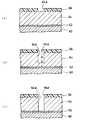
処理容器10内に搬入された半導体ウエハWの主面上には、図2の(a)に示すように、多層配線構造における下層側配線層60、バリア層62、有機系low-k膜(層間絶縁膜)64およびマスク66が下からこの順に積層されている。配線層60は、たとえばCu配線層であり、たとえばデュアルダマシン加工で形成されている。バリア層62は、たとえば1000Å(0.1μm)の膜厚を有する窒化珪素(SiN)膜であり、たとえばCVD(Chemical Vapor Deposition)法により形成されている。有機系low-k膜64は、たとえば1μmの膜厚を有するSiOC系low-k膜であり、たとえばCVD法により形成されている。マスク66は、たとえばレジスト膜であり、通常のレジスト塗布法によって形成されている。また、マスク66は露光・現像によってパターニングされ、ビアホールを形成する位置に開口部66aが形成されている。
【0031】
この実施形態では、かかる半導体ウエハWに対して2ステップ方式のエッチング加工が施される。
【0032】
先ず、第1工程として、第1ステップのプラズマエッチングが行われる。この第1ステップでは、処理ガス供給系よりCHF3/Ar/N2の混合ガスがエッチングガスとして処理容器10のシャワーヘッド18に供給される。一方、高周波電源17より高周波電力がサセプタ16に供給される。エッチング条件の一例として、CHF3/Ar/N2の流量比は20/1000/40sccmに設定され、RF電力のパワーは1700Wに設定される。処理容器10内の圧力はたとえば75mTorrに設定され、ウエハW裏面におけるHe圧力はセンター/エッジでたとえば5/20Torrに設定され、温度は下部電極/上部電極/容器側壁温度で60゜C/60゜C/60゜Cに設定される。
【0033】
こうして、シャワーヘッド18(上部電極)とサセプタ16(下部電極)との間には、ダイポールマグネット54,56による磁界が形成されている空間に高周波電源17からの高周波電界が印加または形成されることによりマグネトロン放電が生じ、この放電空間にエッチングガスつまりCHF3/Ar/N2の混合ガスが送り込まれることでそれらのガス分子が解離してプラズマが発生し、このプラズマから生成された活性種や反応性イオンがサセプタ16上の半導体ウエハWに降下または入射する。この場合、CHF3から解離したHがFラジカルやCFxラジカルと結合してHFやCFx-1を生成することにより、レジストマスク66のエッチングを十分抑えながら、つまり十分高い選択比でSiOC系low-k膜64を垂直形状にエッチングすることができる。
【0034】
この第1ステップのプラズマエッチングは、図2の(b)に示すように、レジスト開口部66a内のSiOC系low-k膜64に形成されるホール64aの底が所定の深さd、たとえば8000Å付近の深さに達したところで、終了する。このエッチングの終了は、処理ガス供給系からのCHF3/Ar/N2の混合ガスの供給を止める、つまり各ガス供給源40,44,46の開閉バルブ40b,44b,46bを閉じるとともに、高周波電源17の出力をオフにすることによって行う。なお、排気系は、処理容器10内の排気を継続する。
【0035】
次に、第2工程として、処理ガス供給系のArガス供給源46よりArガスがパージングガスとして処理容器10内に送り込まれる。これにより、処理容器10内に残留していた水素や水素化合物は他の残留物質と一緒にパージングガスに巻き込まれるようにして排気口10bから排気管52を通って排出される。たとえば、Arガスの流量を1000sccm、排気速度を800リットル/sに設定することで、レジデンスタイム(処理容器内で導入されてから排気されるまでの気体分子の平均滞在時間)を2.48msとすることができる。この場合、このパージング工程の所要時間を数秒程度に設定してよい。なお、パージングガスに用いるArガスは、前工程の第1ステップのプラズマエッチングでもエッチングガスの一組成ガスとして用いられていたので、Arガス供給源46の開閉バルブ46bを開けたまま、第1ステップのプラズマエッチング工程からパージング工程に移行してもよい。
【0036】
上記のようなパージング工程の後に、第3工程として第2ステップのプラズマエッチングが行われる。第2ステップでは、処理ガス供給系よりC4F8/Ar/N2の混合ガスがシャワーヘッド18に供給される。一方、高周波電源17の出力がオンに切り換えられる。エッチング条件の一例として、C4F8/Ar/N2の流量比は5/1000/150sccm(総流量:1155sccm、Ar流量の比率:87%)、RF電力は1700W、圧力は100mTorr、ウエハW裏面におけるHe圧力はセンター/エッジで5/20Torr、温度は下部電極/上部電極/容器側壁で60゜C/60゜C/60゜Cに設定される。
【0037】
この第2ステップのプラズマエッチングでは、図2の(C)に示すように、異方性(垂直形状)を保ったままエッチストップを起こすことなく下地膜62に達するまで、しかも下地膜(窒化珪素膜)62に対して高い選択比で、SiOC系low-k膜64をエッチングすることができる。なお、C4F8/Ar/N2混合ガスはレジストマスク66に対しては選択比が低いという性質がある。しかし、第1ステップで既にSiOC系low-k膜64が相当の割合(約80%)までエッチングされており、第2ステップの負担する所要エッチング量(約20%)が少ないため、レジストマスク66に対する実質的な選択性を得ることができる。
【0038】
上記のように、この実施形態では、CHF3/Ar/N2混合ガスを用いる第1ステップのプラズマエッチングとC4F8/Ar/N2混合ガスを用いる第2ステップのプラズマエッチングとの間にArガスを用いるパージング工程を挿入し、このパージング工程で処理容器10内の残留水素を除去するようにしたので、第2ステップのプラズマエッチングを円滑に進行させ、ホール64aを確実に貫通させることができる。
【0039】
さらに、この実施形態では、第2ステップのプラズマエッチングで使用するC4F8/Ar/N2混合ガスにおいて、総流量に対するAr流量の比率を80%以上に設定している。この条件により、Arイオンによるスパッタ力を向上させて、ホール64aの側壁に堆積するカーボン系ポリマーを効果的に除去するとともに、カーボン系ポリマーをホール内奥に侵入させて下地膜(窒化珪素膜)62上に堆積させることができる。これによって、下地膜(窒化珪素膜)62に対するするフッ素系ラジカルのエッチング作用を低減させ、選択比を向上させることができる。
【0040】
この実施形態の第2工程では、上記のようなパージング工程に代えて、O2プラズマによるフラッシュを行うことも可能である。より詳細には、第1ステップのプラズマエッチングを終了した時点で、エッチングガスつまりCHF3/Ar/N2混合ガスの供給を止めるとともに、いったん高周波電源17の出力をオフにしてプラズマを完全に消す。次いで、O2ガス供給源48よりO2ガスを処理容器10に送り込むとともに、高周波電源17の出力をオンに切り換えて、処理空間にO2プラズマを発生させる。このO2プラズマ中のOラジカルが残留水素と反応して水蒸気が生成する。こうして生成した水蒸気は速やかに排気口10aから排気される。
【0041】
別の残留水素除去方法として、第2工程において、処理容器10へのガス供給を止め高周波電源17の出力をオフにしたまま、排気系による排気を所定時間たとえば10秒程度持続させることによっても、相当量の残留水素を処理容器10から排出することができる。
【0042】
あるいは、この実施形態によるエッチング装置(図1)をたとえばクラスタ構成で複数台たとえば2台近接配置し、1つのエッチング装置で第1ステップのプラズマエッチングを実行したなら、半導体ウエハWを基板搬送機構によって別のエッチング装置へ移送し、残留水素の問題が無い移送先のエッチング装置で第2ステップのプラズマエッチングを実行してもよい。
【0043】
上記の実施形態では第1ステップのプラズマエッチングでCHF3/Ar/N2混合ガスを使用し、第2ステップのプラズマエッチングでC4F8/Ar/N2混合ガスを使用したが、絶縁膜材料、マスク材料、下地材料等に応じてエッチングガスの種類または成分を種々変形または選択できる。たとえば、フロロカーボンガスにH2ガスを添加した混合ガスを第1ステップ用の第1のエッチングガスとすることも可能である。また、下地膜62を炭化珪素膜(SiC)とすることも可能である。
【0044】
【発明の効果】
以上説明したように、本発明のエッチング方法によれば、良好な異方性(垂直)形状とマスクおよび下地膜の双方に対する高い選択比を確保しつつ絶縁膜を安定確実にエッチングすることができる。
【図面の簡単な説明】
【図1】本発明の一実施形態によるエッチング方法を実施するためのエッチング装置の構成を示す断面図である。
【図2】実施形態によるエッチング方法の作用を示す断面図である。
【符号の説明】
10 反応容器
10b 排気口
16 サセプタ
17 高周波電源
18 シャワーヘッド
40 CHF3ガス供給源
42 C4F8ガス供給源
44 N2ガス供給源
46 Arガス供給源
48 O2ガス供給源
54 ダイポールリングマグネット[0001]
BACKGROUND OF THE INVENTION
The present invention relates to a technique for etching an insulating film, and more particularly to an etching method suitable for use in etching an interlayer insulating film in a multilayer wiring structure.
[0002]
[Prior art]
Semiconductor devices are required to have a low dielectric constant of an interlayer insulating film in conjunction with miniaturization and high speed of wiring. Recently, an organic low dielectric constant (low-k) film, particularly a SiCO-based low dielectric constant is required. The -k film is drawing attention.
[0003]
Conventionally, a mixed gas containing a fluorocarbon-based gas as a main etchant gas has been used as an etching gas for an organic low-k film. For example, in the plasma etching for forming a contact hole (via hole), a silicon nitride film on an organic low-k film as a base film, a high selectivity for the silicon nitride film of the substrate material C4 F8 / Ar / N A mixed gas of2 is frequently used. However, the C4 F8 / Ar / N2 mixed gas has a limitation in the etching rate of the low-k film and has low selectivity to the resist film as a mask pattern, and an anisotropic (vertical) shape can be obtained. It can be difficult.
[0004]
Therefore, instead of the etching method using the C4 F8 gas as described above, the organic low-k film is first used as the etching gas as the CHF3 / Ar / N2 mixed gas as the film surface of the mask opening. Two steps of etching to a predetermined depth, switching the etching gas to a C4 F8 / Ar / N2 mixed gas, and continuing the etching, and ending the etching when reaching the lower layer or the underlying silicon nitride film A scheme has been proposed.
[0005]
In this two-step method, in the first step plasma etching using a CHF3 / Ar / N2 mixed gas, the resist is difficult to etch because the amount of F radicals is relatively small. On the other hand, organic low-k films react well with active species and ions in the plasma, and volatile products such as SiFx , COx , and CNH are efficiently generated, and etched into a vertical shape at a high etching rate. Is done. However, the CHF3 / Ar / N2 mixed gas is inferior to the base film (silicon nitride film), so it is necessary to switch to a C4 F8 / Ar / N2 mixed gas with a high selectivity from the middle. is there.
[0006]
[Problems to be solved by the invention]
However, in the conventional two-step method as described above, immediately after switching to the plasma etching of the second step, the progress of the etching is extremely reduced, the via hole diameter is tapered (tapered), or the etching is low-k. There was a possibility that it would be easy to stop in the middle of the film (before reaching the base film).
[0007]
An object of the present invention isto provide a highly anisotropic (vertical) shape and etching method to the insulating film while ensuring a high selectivity for both the mask and the underlying film can be stably reliably etchedis there.
[0008]
[Means for Solving the Problems]
In order to achieve the above object,an insulating film etching methodaccording to a first aspect of the present invention generates an etching gas plasma in a processing vessel, and forms an insulating film on a substrate to be processed in an atmosphere of the plasma. a method of etching through a mask pattern, a first step of carbon into the processing chamber, introducing a first etching gas containing fluorine and hydrogen, etching the insulating film to a desired depth,the processing Introducing an inert gas into the container and purging the processing container with the inert gas while turning off the plasma, thereby removing at least one of hydrogen and hydrogen compounds remainingin the processing container A second step of discharging out of the processing vessel, and introducing a second etching gas containing carbon and fluorine and not hydrogen into the processing vessel; And a third step of etching the serial insulating film continued.
[0009]
According to the etching method of the present invention, in the first step of plasma etching, H (hydrogen) contained in the first etching gas is combined with F (fluorine) radicals or CFx radicals to generate HF, A small amount of CF, CF2 or their polymer film is deposited on the surface of the mask pattern to suppress the etching or peeling. On the other hand, in the opening of the mask pattern, O (oxygen) atoms generated by the etching of an insulating film CF, CF2 and reacting with volatile COx, COF, to generate the COF2, etching proceeds.
[0010]
When plasma etching in the first step (first step) is stopped, atoms and compounds that have been active species and ions until then are released from the plasma and remain in the processing vessel. In addition, some of the first etching gas that has been introduced into the processing container until then remains. Among these residual substances, hydrogen or hydrogen compounds are contained. If the process proceeds to the second step of plasma etching as in the prior art, the residual hydrogen deposits a CH-based polymer near the bottom of the hole, or a main etchant such as a nitrogen radical reacts with it to substantially Or the etching progresses.
[0011]
Therefore, in the present invention, if plasma etching in the first step (first step) is stopped, at least one of hydrogen and hydrogen compounds remaining in the processing vessel in the second step is discharged out of the vessel, and then the second step The second step of plasma etching is performed in three steps. In this second step of plasma etching, the second etching gas itself does not contain hydrogen and the residual hydrogen is also removed, so that the above-described etching failure (particularly etch stop) caused by hydrogen does not occur. Etching can proceed or continue stably.
[0012]
In the second step, the inside of the processing vessel is purged with an inert gaswhile the plasma is turned off. In this case, when the first etching gas used in the plasma etching in the first step (first step) includes an inert gas (for example, Ar), the same type of inert gas (Ar) is used as the purging gas. Is preferred.By purgingwith an inert gaswith the plasma turned off, hydrogen and hydrogen compounds remaining in the processing vessel can be efficiently removed in a short time.
[0013]
According to a second aspect of the present invention, there is provided a method for etching an insulating film in which a plasma of an etching gas is generated in a processing vessel, and the insulating film on the substrate to be processed is etched through a mask pattern in the plasma atmosphere. A first etching gas containing carbon, fluorine, and hydrogen is introduced into the processing container to etch the insulating film to a desired depth, and a new gas is introduced into the processing container. Without exhausting the plasma, the inside of the processing vessel is evacuated for a predetermined time or longer, thereby discharging at least one of hydrogen and hydrogen compounds remaining in the processing vessel to the outside of the processing vessel. And etching the insulating film by introducing a second etching gas containing carbon and fluorine and not hydrogen into the processing vessel. And a third step.
[0014]
In the second etching method, if the plasma etching in the first step (first step) is stopped, the inside of the processing vessel is maintained for a predetermined time (with the plasma turned off without introducing a new gas in the second step). For example, at least one of hydrogen and a hydrogen compound remaining in the processing container is discharged out of the container by evacuating for 10 seconds or more, and the second step of plasma etching is performed in the third process thereafter. In this second step of plasma etching, the second etching gas itself does not contain hydrogen and the residual hydrogen is also removed, so that the above-described etching failure (particularly etch stop) caused by hydrogen does not occur. Etching can proceed or continue stably.
[0017]
The etching method of the present invention is effective for an organic insulating film, particularly a SiOC-based low dielectric constant film, and can provide a remarkable effect in etching for forming a connection hole. In this specification, the SiOC film is defined as an organic film. The mask pattern may typically be formed of a resist film, and the base film may be a nitride film such as a silicon nitride film. Moreover, silicon carbide may be sufficient.
[0018]
In the etching method of the present invention, a preferred form of the first etching gas is a mixed gas containing a hydrofluorocarbon gas, an N2 gas, and an inert gas. In addition, a preferred form of the second etching gas is a mixed gas containing a fluorocarbon gas, N2 gas, and an inert gas. The inert gas is preferably Ar, but He, Ne, and Kr can also be used. The hydrofluorocarbon gas is typically CHF3, but may be CH2 F2 , CH3 F, or C2 H2 F4 . Fluorocarbon gas is typically C4 F8, but C2 F4 , C3 F6 , C3 F8 , C4 F6 , C5 F8 (linear and cyclic isomers are included). Included).
[0019]
DETAILED DESCRIPTION OF THE INVENTION
Hereinafter, preferred embodiments of the present invention will be described.
[0020]
FIG. 1 shows the configuration of an etching apparatus for carrying out an etching method according to an embodiment of the present invention.
[0021]
The etching apparatus has a
[0022]
An upper surface of the
[0023]
The
[0024]
Inside the
[0025]
The
[0026]
The main
[0027]
A substrate entrance /
[0028]
Next, an etching method according to an embodiment that can be performed by the etching apparatus as described above will be described. In this embodiment, a connection hole (via hole) is formed in the organic low-k film as an interlayer insulating film by plasma etching.
[0029]
First, in the etching apparatus (FIG. 1), the
[0030]
On the main surface of the semiconductor wafer W carried into the
[0031]
In this embodiment, the semiconductor wafer W is subjected to a two-step etching process.
[0032]
First, as a first process, plasma etching of a first step is performed. In this first step, a mixed gas of CHF3 / Ar / N2 is supplied as an etching gas from the processing gas supply system to the
[0033]
Thus, a high-frequency electric field from the high-
[0034]
In this first step of plasma etching, as shown in FIG. 2B, the bottom of the
[0035]
Next, as a second step, Ar gas is sent into the
[0036]
After the purging process as described above, a second step of plasma etching is performed as a third process. In the second step, a mixed gas of C4 F8 / Ar / N2 is supplied to the
[0037]
In this second step of plasma etching, as shown in FIG. 2C, the base film (silicon nitride) is reached until the
[0038]
As described above, in this embodiment, between the first step plasma etching using the CHF3 / Ar / N2 mixed gas and the second step plasma etching using the C4 F8 / Ar / N2 mixed gas. Since a purging process using Ar gas is inserted into the chamber and residual hydrogen in the
[0039]
Further, in this embodiment, in the C4 F8 / Ar / N2 mixed gas used in the second step plasma etching, the ratio of the Ar flow rate to the total flow rate is set to 80% or more. Under these conditions, the sputtering force by Ar ions is improved, and the carbon-based polymer deposited on the sidewall of the
[0040]
In the second step of this embodiment, it is possible to perform flash with O2 plasma instead of the purging step as described above. More specifically, when the plasma etching of the first step is completed, the supply of the etching gas, that is, the CHF3 / Ar / N2 mixed gas is stopped, and the output of the high-
[0041]
As another method for removing residual hydrogen, in the second step, the gas supply to the
[0042]
Alternatively, if a plurality of, for example, two etching apparatuses (FIG. 1) according to this embodiment are arranged close to each other in a cluster configuration and the first step of plasma etching is performed with one etching apparatus, the semiconductor wafer W is moved by the substrate transfer mechanism. The plasma etching of the second step may be performed by a transfer destination etching apparatus that is transferred to another etching apparatus and has no problem of residual hydrogen.
[0043]
In the above embodiment, the CHF3 / Ar / N2 mixed gas is used in the first step plasma etching, and the C4 F8 / Ar / N2 mixed gas is used in the second step plasma etching. Various types or components of the etching gas can be modified or selected depending on the material, mask material, base material, and the like. For example, a mixed gas obtained by adding H2 gas to fluorocarbon gas can be used as the first etching gas for the first step. Further, the
[0044]
【The invention's effect】
As described above, according to the etching method of the present invention, it is possible to stably and reliably etch the insulating film while ensuring a good anisotropic (vertical) shape and a high selection ratio with respect to both the mask and the base film. .
[Brief description of the drawings]
FIG. 1 is a cross-sectional view showing a configuration of an etching apparatus for performing an etching method according to an embodiment of the present invention.
FIG. 2 is a cross-sectional view showing the operation of the etching method according to the embodiment.
[Explanation of symbols]
10 reaction vessel
Claims (11)
Translated fromJapanese前記処理容器内に炭素、フッ素および水素を含む第1のエッチングガスを導入して、前記絶縁膜を所望の深さまでエッチングする第1の工程と、
前記処理容器内に不活性ガスを導入して、プラズマをオフにしたまま前記不活性ガスによって前記処理容器内をパージングすることにより、前記処理容器内に残留していた水素および水素化合物の少なくとも一方を前記処理容器の外へ排出する第2の工程と、
前記処理容器内に炭素およびフッ素を含み水素を含まない第2のエッチングガスを導入して、前記絶縁膜のエッチングを引き続き行う第3の工程と
を有する絶縁膜のエッチング方法。In a method for generating an etching gas plasma in a processing container and etching an insulating film on a substrate to be processed through a mask pattern under the plasma atmosphere,
Introducing a first etching gas containing carbon, fluorine and hydrogen into the processing vessel to etch the insulating film to a desired depth;
By introducing an inert gas into the processing container and purging the processing container with the inert gas while turning off the plasma , at least one of hydrogen and a hydrogen compound remainingin the processing container A second step of discharging the gas out of the processing container;
And a third step of continuously etching the insulating film by introducing a second etching gas containing carbon and fluorine but not hydrogen into the processing container.
前記処理容器内に炭素、フッ素および水素を含む第1のエッチングガスを導入して、前記絶縁膜を所望の深さまでエッチングする第1の工程と、
前記処理容器内に新たなガスを導入することなく、プラズマをオフにしたまま前記処理容器内を所定時間以上排気することにより、前記処理容器内に残留していた水素および水素化合物の少なくとも一方を前記処理容器の外へ排出する第2の工程と、
前記処理容器内に炭素およびフッ素を含み水素を含まない第2のエッチングガスを導入して、前記絶縁膜のエッチングを引き続き行う第3の工程と
を有する絶縁膜のエッチング方法。In a method for generating an etching gas plasma in a processing container and etching an insulating film on a substrate to be processed through a mask pattern under the plasma atmosphere,
Introducing a first etching gas containing carbon, fluorine and hydrogen into the processing vessel to etch the insulating film to a desired depth;
Without introducing a new gas into the processing vessel, the processing vessel is evacuated for a predetermined time or more with the plasma turned off, thereby removing at least one of hydrogen and hydrogen compounds remainingin the processing vessel. A second step of discharging out of the processing vessel;
And a third step of continuously etching the insulating film by introducing a second etching gas containing carbon and fluorine but not hydrogen into the processing container.
Priority Applications (2)
| Application Number | Priority Date | Filing Date | Title |
|---|---|---|---|
| JP2002248074AJP4071069B2 (en) | 2002-08-28 | 2002-08-28 | Insulating film etching method |
| US10/653,707US6967171B2 (en) | 2002-08-28 | 2003-08-28 | Insulation film etching method |
Applications Claiming Priority (1)
| Application Number | Priority Date | Filing Date | Title |
|---|---|---|---|
| JP2002248074AJP4071069B2 (en) | 2002-08-28 | 2002-08-28 | Insulating film etching method |
Publications (2)
| Publication Number | Publication Date |
|---|---|
| JP2004087875A JP2004087875A (en) | 2004-03-18 |
| JP4071069B2true JP4071069B2 (en) | 2008-04-02 |
Family
ID=32055536
Family Applications (1)
| Application Number | Title | Priority Date | Filing Date |
|---|---|---|---|
| JP2002248074AExpired - Fee RelatedJP4071069B2 (en) | 2002-08-28 | 2002-08-28 | Insulating film etching method |
Country Status (2)
| Country | Link |
|---|---|
| US (1) | US6967171B2 (en) |
| JP (1) | JP4071069B2 (en) |
Families Citing this family (22)
| Publication number | Priority date | Publication date | Assignee | Title |
|---|---|---|---|---|
| US7311852B2 (en)* | 2001-03-30 | 2007-12-25 | Lam Research Corporation | Method of plasma etching low-k dielectric materials |
| US7112534B2 (en)* | 2003-09-25 | 2006-09-26 | Intel Corporation | Process for low k dielectric plasma etching with high selectivity to deep uv photoresist |
| US7740737B2 (en) | 2004-06-21 | 2010-06-22 | Tokyo Electron Limited | Plasma processing apparatus and method |
| US7951262B2 (en) | 2004-06-21 | 2011-05-31 | Tokyo Electron Limited | Plasma processing apparatus and method |
| TWI574318B (en) | 2004-06-21 | 2017-03-11 | Tokyo Electron Ltd | A plasma processing apparatus, a plasma processing method, and a computer-readable recording medium |
| US7988816B2 (en) | 2004-06-21 | 2011-08-02 | Tokyo Electron Limited | Plasma processing apparatus and method |
| JP4550507B2 (en)* | 2004-07-26 | 2010-09-22 | 株式会社日立ハイテクノロジーズ | Plasma processing equipment |
| US7326358B2 (en)* | 2004-09-27 | 2008-02-05 | Tokyo Electron Limited | Plasma processing method and apparatus, and storage medium |
| JP4515309B2 (en)* | 2005-03-31 | 2010-07-28 | 東京エレクトロン株式会社 | Etching method |
| JP4707178B2 (en)* | 2005-06-29 | 2011-06-22 | キヤノンマーケティングジャパン株式会社 | Etching method and etching apparatus |
| JP5103738B2 (en)* | 2006-01-12 | 2012-12-19 | パナソニック株式会社 | Atmospheric pressure plasma processing method and apparatus |
| JP5192209B2 (en) | 2006-10-06 | 2013-05-08 | 東京エレクトロン株式会社 | Plasma etching apparatus, plasma etching method, and computer-readable storage medium |
| US20080083700A1 (en)* | 2006-10-10 | 2008-04-10 | Lexmark International, Inc. | Method and Apparatus for Maximizing Cooling for Wafer Processing |
| JP2008181996A (en)* | 2007-01-24 | 2008-08-07 | Tokyo Electron Ltd | Method of manufacturing semiconductor device, apparatus of manufacturing semiconductor device, control program, and computer storage medium |
| JP5264834B2 (en)* | 2010-06-29 | 2013-08-14 | 東京エレクトロン株式会社 | Etching method and apparatus, semiconductor device manufacturing method |
| JP6081176B2 (en)* | 2012-12-12 | 2017-02-15 | 東京エレクトロン株式会社 | Plasma etching method and plasma etching apparatus |
| US10297496B2 (en)* | 2017-03-15 | 2019-05-21 | Tokyo Electron Limited | Method for processing target objection |
| JP2018157188A (en)* | 2017-03-15 | 2018-10-04 | 東京エレクトロン株式会社 | Method of processing workpiece |
| JP6929148B2 (en)* | 2017-06-30 | 2021-09-01 | 東京エレクトロン株式会社 | Etching method and etching equipment |
| US10811320B2 (en)* | 2017-09-29 | 2020-10-20 | Taiwan Semiconductor Manufacturing Company, Ltd. | Footing removal in cut-metal process |
| CN116940124A (en) | 2018-12-27 | 2023-10-24 | 联华电子股份有限公司 | Semiconductor element and manufacturing method thereof |
| US11508402B1 (en) | 2021-09-16 | 2022-11-22 | Western Digital Technologies, Inc. | Slider assemblies having recesses with solder structures for magnetic recording devices, and related methods of forming slider assemblies |
Family Cites Families (5)
| Publication number | Priority date | Publication date | Assignee | Title |
|---|---|---|---|---|
| US6451703B1 (en)* | 2000-03-10 | 2002-09-17 | Applied Materials, Inc. | Magnetically enhanced plasma etch process using a heavy fluorocarbon etching gas |
| JP2002270586A (en)* | 2001-03-08 | 2002-09-20 | Tokyo Electron Ltd | Etching method of organic based insulating film and dual damascene process |
| US6712983B2 (en)* | 2001-04-12 | 2004-03-30 | Memsic, Inc. | Method of etching a deep trench in a substrate and method of fabricating on-chip devices and micro-machined structures using the same |
| JP2003124189A (en)* | 2001-10-10 | 2003-04-25 | Fujitsu Ltd | Method for manufacturing semiconductor device |
| US20040171273A1 (en)* | 2003-02-28 | 2004-09-02 | Masatoshi Oyama | Specimen surface processing apparatus and surface processing method |
- 2002
- 2002-08-28JPJP2002248074Apatent/JP4071069B2/ennot_activeExpired - Fee Related
- 2003
- 2003-08-28USUS10/653,707patent/US6967171B2/ennot_activeExpired - Lifetime
Also Published As
| Publication number | Publication date |
|---|---|
| US6967171B2 (en) | 2005-11-22 |
| JP2004087875A (en) | 2004-03-18 |
| US20050112879A1 (en) | 2005-05-26 |
Similar Documents
| Publication | Publication Date | Title |
|---|---|---|
| JP4071069B2 (en) | Insulating film etching method | |
| US10770346B2 (en) | Selective cobalt removal for bottom up gapfill | |
| US10049891B1 (en) | Selective in situ cobalt residue removal | |
| KR102360220B1 (en) | Methods for etching a dielectric barrier layer in a dual damascene structure | |
| US7977390B2 (en) | Method for plasma etching performance enhancement | |
| TWI520212B (en) | Selective titanium nitride etching | |
| US6991739B2 (en) | Method of photoresist removal in the presence of a dielectric layer having a low k-value | |
| JP5038567B2 (en) | Etching method | |
| JP4825911B2 (en) | Plasma etching and photoresist strip process with defluorination and wafer defluorination steps in intervening chamber | |
| US8383519B2 (en) | Etching method and recording medium | |
| US20040072443A1 (en) | Method for plasma etching performance enhancement | |
| US20090221148A1 (en) | Plasma etching method, plasma etching apparatus and computer-readable storage medium | |
| JP5116983B2 (en) | Plasma processing method and plasma processing apparatus | |
| CN100521111C (en) | Plasma etching method | |
| KR20050118267A (en) | A method for plasma etching performance enhancement | |
| US20040106293A1 (en) | Method for etching organic insulating film and dual damasene process | |
| US7129171B2 (en) | Selective oxygen-free etching process for barrier materials | |
| TWI751326B (en) | Self-aligned via process flow | |
| JP2008198659A (en) | Plasma etching method | |
| US20240290623A1 (en) | Processing methods to improve etched silicon-and-germanium-containing material surface roughness | |
| JP4827567B2 (en) | Plasma etching method and computer-readable storage medium | |
| JP4216922B2 (en) | Oxide film etching method | |
| JP2001118825A (en) | Etching method | |
| US20070218699A1 (en) | Plasma etching method and computer-readable storage medium | |
| US20240282585A1 (en) | Treatments to improve etched silicon-and-germanium-containing material surface roughness |
Legal Events
| Date | Code | Title | Description |
|---|---|---|---|
| A621 | Written request for application examination | Free format text:JAPANESE INTERMEDIATE CODE: A621 Effective date:20050802 | |
| A977 | Report on retrieval | Free format text:JAPANESE INTERMEDIATE CODE: A971007 Effective date:20070612 | |
| A131 | Notification of reasons for refusal | Free format text:JAPANESE INTERMEDIATE CODE: A131 Effective date:20070703 | |
| A521 | Written amendment | Free format text:JAPANESE INTERMEDIATE CODE: A523 Effective date:20070903 | |
| TRDD | Decision of grant or rejection written | ||
| A01 | Written decision to grant a patent or to grant a registration (utility model) | Free format text:JAPANESE INTERMEDIATE CODE: A01 Effective date:20080115 | |
| A61 | First payment of annual fees (during grant procedure) | Free format text:JAPANESE INTERMEDIATE CODE: A61 Effective date:20080116 | |
| R150 | Certificate of patent or registration of utility model | Free format text:JAPANESE INTERMEDIATE CODE: R150 | |
| FPAY | Renewal fee payment (event date is renewal date of database) | Free format text:PAYMENT UNTIL: 20110125 Year of fee payment:3 | |
| FPAY | Renewal fee payment (event date is renewal date of database) | Free format text:PAYMENT UNTIL: 20110125 Year of fee payment:3 | |
| FPAY | Renewal fee payment (event date is renewal date of database) | Free format text:PAYMENT UNTIL: 20140125 Year of fee payment:6 | |
| LAPS | Cancellation because of no payment of annual fees |