JP4069963B2 - MOS transistor threshold compensation circuit and flip-flop type sense amplifier having the same - Google Patents
MOS transistor threshold compensation circuit and flip-flop type sense amplifier having the sameDownload PDFInfo
- Publication number
- JP4069963B2 JP4069963B2JP30325396AJP30325396AJP4069963B2JP 4069963 B2JP4069963 B2JP 4069963B2JP 30325396 AJP30325396 AJP 30325396AJP 30325396 AJP30325396 AJP 30325396AJP 4069963 B2JP4069963 B2JP 4069963B2
- Authority
- JP
- Japan
- Prior art keywords
- threshold value
- switch element
- capacitor
- mos transistor
- circuit
- Prior art date
- Legal status (The legal status is an assumption and is not a legal conclusion. Google has not performed a legal analysis and makes no representation as to the accuracy of the status listed.)
- Expired - Fee Related
Links
Images


Landscapes
- Static Random-Access Memory (AREA)
- Electronic Switches (AREA)
- Dram (AREA)
Description
Translated fromJapanese【0001】
本発明は、MOSトランジスタ敷居値補償回路及びこれを備えたフリップフロップ型センスアンプに関する。
【0002】
【従来の技術】
図11は、DRAMに用いられている従来のフリップフロップ型センスアンプを示す。
図中、21及び22はnMOSトランジスタであり、23及び24はpMOSトランジスタである。nMOSトランジスタ21とpMOSトランジスタ23とからなるCMOSインバータの入力端にはビット線*BLが接続され、nMOSトランジスタ22とpMOSトランジスタ24とからなるCMOSインバータの入力端にはビット線BLが接続されている。一方のCMOSインバータの入力端及び出力端はそれぞれ、他方のCMOSインバータの出力端及び入力端に接続されている。ビット線BL及び*BLには、不図示のメモリセルが接続されている。
【0003】
このメモリセルからデータを読み出す場合、まず、ビット線BL及び*BLが電位Vcc/2にプリチャージされ、次に、ワード線が活性化されてメモリセルが選択され、その記憶内容がビット線BLに読み出されて両ビット線間に電位差が生じ、これがセンスアンプ20で増幅される。
ビット線BL及び*BLの浮遊容量がメモリセルの容量の数十倍と大きいため、増幅前のビット線間の電位差は例えば70mVと僅かである。このため、nMOSトランジスタ21とnMOSトランジスタ22の敷居値に差があると、ビット線間の電位差が逆方向に増幅されて誤読み出しが生ずる原因となる。また、メモリセル容量の微小化を制限して増幅前のビット線間の電位差を所定値以上にすることにより誤読み出しを防止しようとすると、回路素子の微細化が制限されてDRAMの記憶容量が犠牲になる。
【0004】
MOSトランジスタの敷居値は、製造プロセスのばらつきによりゲート長が短くなると減少し、ゲート幅が小さくなると増加する。半導体回路素子の微細化に伴い、ショートチャンネル効果やナロウチャンネル効果等が現れて、ゲート長やゲート幅の僅かなばらつきがMOSトランジスタの敷居値を大きく変化させ、隣合うMOSトランジスタの敷居値に差が生ずる。
【0005】
このばらつきを補償するため、ウエルの電位を変化させる方法があるが、この方法は、ブロック単位で敷居値のばらつきを補償する場合にのみ有効である。
隣接したトランジスタの敷居値を補償する従来の回路は、センス動作毎に敷居値を補償する動作が必要であるため、動作の高速化が妨げられる。また、敷居値補償動作とセンス動作とでトランジスタのソースとドレインとが逆になる方式の場合には、トランジスタの敷居値に方向性があるとき、補償が不正確になる。
【0006】
【発明が解決しようとする課題】
そこで、本発明者は、トランジスタのゲートにコンデンサを接続し、コンデンサのゲート側電極とこれに接続されたゲートとを疑似フローティングゲートにし、敷居値に応じスイッチ素子を介してこの疑似フローティングゲートに電荷を蓄えさせることにより、コンデンサの一対の電極のうちゲートに非接続の電極(疑似制御電極)から見たトランジスタの敷居値を所定値にする構成を案出し出願した。
【0007】
この構成によれば、上記のような問題点を解決することができる。
しかし、敷居値補償動作時に、補償されるトランジスタに貫通電流が流れるので、若干ではあるが消費電流が増加する。
本発明の目的は、このような問題点に鑑み、敷居値補償動作時の消費電流を低減することが可能なMOSトランジスタ敷居値補償回路及びこれを備えたフリップフロップ型センスアンプを提供することにある。
【0008】
本発明の第1態様では、通常動作時にソースが一定電位にされるMOSトランジスタの敷居値を補償する回路において、
該MOSトランジスタのドレインとゲートとの間に接続された第1スイッチ素子と、
信号供給線と該ゲートとの間に接続された第1コンデンサと、
電源供給線と該ドレインとの間に直列接続された第2コンデンサ及び第2スイッチ素子と、
敷居値補償時において、該ソースが該一定電位にされ該信号供給線が参照電位にされた状態で、該第1スイッチ素子及び該第2スイッチ素子をオンにすることにより該MOSトランジスタをオンにさせ次いで該第2スイッチ素子をオフにした後該第1スイッチ素子をオフにする制御回路と、
を有する。
【0009】
上記MOSトランジスタがnMOSトランジスタである場合、敷居値補償時において、第1スイッチ素子及び第2スイッチ素子がオンになると、ゲートに正電荷が蓄積されてゲート電位が上昇しnMOSトランジスタがオンになり、次いで第2スイッチ素子がオフになると、この蓄積された電荷の一部が、オン状態のnMOSトランジスタのドレイン・ソース間を通って放電され、ゲート・ソース間がほぼ敷居値又は敷居値になるとnMOSトランジスタがほぼオフ又はオフになる。次いで第1スイッチ素子がオフになると、nMOSトランジスタのゲートとこれに接続された第1コンデンサの一方の電極と両者間の配線とが疑似フローティングゲートになり、これに蓄えられた電荷により、第1コンデンサの他方の電極(疑似制御電極)から見たnMOSトランジスタの敷居値が所望の値になる。
上記MOSトランジスタがpMOSトランジスタである場合、敷居値補償時において、第1スイッチ素子及び第2スイッチ素子がオンになると、ゲートに負電荷が蓄積されてゲート電位が下降しpMOSトランジスタがオンになり、次いで第2スイッチ素子がオフになると、この蓄積された電荷の一部が、オン状態のnMOSトランジスタのドレイン・ソース間を通って放電され、ゲート・ソース間がほぼ敷居値又は敷居値になるとpMOSトランジスタがほぼオフ又はオフになる。次いで第1スイッチ素子がオフになると、nMOSトランジスタのゲートとこれに接続された第1コンデンサの一方の電極と両者間の配線とが疑似フローティングゲートになり、これに蓄えられた電荷により、第1コンデンサの他方の電極(疑似制御電極)から見たpMOSトランジスタの敷居値が所望の値になる。
電源供給線とMOSトランジスタのドレインとの間に第2コンデンサ及び第2スイッチ素子が直列接続されているので、第2スイッチ素子をオンにした状態でMOSトランジスタに流れる電流が、第2コンデンサの部分を短絡した場合よりも少なくなり、消費電流を低減することができるという効果を奏する。
【0016】
本発明の第2態様では、上記第2コンデンサはその一端が上記電源供給線に接続され、
複数の上記MOSトランジスタの各々について上記第1スイッチ素子と上記第1コンデンサと上記第2スイッチ素子とを備え、
該第2コンデンサの他端が該複数の該第2スイッチ素子の各々の一端に共通に接続されている。
【0017】
この構成によれば、第2コンデンサの他端が複数の第2スイッチ素子の各々の一端に共通に接続されているので、複数のMOSトランジスタに対するMOSトランジスタ敷居値補償回路の構成が全体として簡単になるという効果を奏する。
本発明の第3態様では、上記第2スイッチ素子はその一端が上記電源供給線に接続され、
複数の上記MOSトランジスタの各々について上記第1スイッチ素子と上記第1コンデンサと上記第2コンデンサとを備え、
該第2スイッチ素子の他端が該複数の該第2コンデンサの各々の一端に共通に接続されている。
【0018】
この構成によれば、第2スイッチ素子の他端が複数の第2コンデンサの各々の一端に共通に接続されているので、複数のMOSトランジスタに対するMOSトランジスタ敷居値補償回路の構成が全体として簡単になるという効果を奏する。
本発明の第4態様では、例えば図7に示す如く、第1のCMOSインバータ(21、23)と第2のCMOSインバータ(22、24)とがクロス接続されたフリップフロップ型センスアンプ回路において、
上記いずれか1つのMOSトランジスタ敷居値補償回路が、該第1のCMOSインバータを構成する一方のMOSトランジスタ(21)に接続され、
上記第1コンデンサ(C1)の1対の電極のうち該MOSトランジスタのゲートと非接続の電極が、該第2のCMOSインバータの出力端に接続され、
該MOSトランジスタのドレインと該第1のCMOSインバータを構成する他方のMOSトランジスタ(23)のドレインとの間に第3スイッチ素子(SW0)が接続され、
上記制御回路は、上記敷居値補償時に該第3スイッチ素子をオフにする。
【0019】
この構成によれば、製造ブロセスのばらつきによりMOSトランジスタ自体の敷居値Vthにばらつきがあっても、第1コンデンサの一方側から見たMOSトランジスタの敷居値VTHを設定値にすることができるので、微小電位差を正確に増幅することが可能となり、誤読み出しが防止され、これにより回路素子のより微細化が可能になるという効果を奏する。
【0021】
【発明の実施の形態】
以下、図面に基づいて本発明の実施形態を説明する。
[第1実施形態]
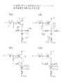
図1は、本発明の第1実施形態のnMOSトランジスタ敷居値補償回路を示す。
【0022】
nMOSトランジスタ21は、通常動作時の回路の一部であり、そのドレインDには、スイッチ素子SW0〜SW2の各々の一端が接続されている。このドレインDは、スイッチ素子SW0を介して通常動作時の回路の他の部分(不図示)に接続されており、スイッチ素子SW0は、敷居値補償動作時にドレインDをこの他の部分から切り離すためのものである。
【0023】
スイッチ素子SW1の他端は、nMOSトランジスタ21のゲートG及びコンデンサC1の一方の電極N1に接続され、コンデンサC1の他方の電極P1に入力信号Vinが供給される。スイッチ素子SW1がオフのときには、ゲートGと電極N1とこの間の接続線とが、nMOSトランジスタ21の疑似フローティングゲートになり、電極P1がnMOSトランジスタ21の疑似制御電極になっている。
【0024】
疑似フローティングゲートに蓄えられる電荷をΔq、電極P1上及びN1上の電荷をそれぞれ+q、−qとすると、ゲートGの電荷はq+Δqとなる。ゲートGと電極P1との電位差をΔV、ゲートGの電位をVfとすると、Vf=Vin+ΔVとなる。nMOSトランジスタ21自体の敷居値をVthとすると、疑似制御電極P1から見たnMOSトランジスタ21の敷居値VTHはVth−ΔVになるので、この敷居値VTHは、疑似フローティングゲートに蓄えられる電荷Δqを調整することにより変更することができる。
【0025】
スイッチ素子SW2の他端はコンデンサC2の一方の電極N2に接続され、コンデンサC2の他方の電極P2は電源供給線Vccに接続されている。
nMOSトランジスタ21のソースSには、電位Vgが印加される。
敷居値補償動作時には、電位Vgは一定にされ、入力信号Vinの値は、電位Vgに所望の敷居値VTHを加算した値の電位Vrefにされる。電源供給線の電位Vcc、電位Vg及びVrefはそれぞれ、例えば1.0V、0.3V及び0.5Vである。上述のようにnMOSトランジスタ21が通常動作時の回路の一部であるので、敷居値補償動作時において電位Vgは、nMOSトランジスタ21が通常動作時のソース電位にされる。
【0026】
敷居値補償動作は、制御回路10がスイッチ素子SW0〜SWS2をオン/オフ制御することにより行われる。
次に、上記の如く構成された本第1実施形態の動作を説明する。
図2は、図1の制御回路10によるスイッチ素子SW0〜SW2の制御及びゲート電位Vfの変化を示す。図2中の期間B〜Dはそれぞれ、図3(B)〜(D)の状態に対応している。
【0027】
図3(A)は、nMOSトランジスタ21の通常使用状態を示しており、スイッチ素子SW0がオン、スイッチ素子SW1及びSW2がオフになっている。
この状態からスイッチ素子SW0がオフにされて、通常使用状態でドレインD接続されていた回路が切り離され、また、スイッチ素子SW1がオン、スイッチ素子SW2がオンにされて、図3(B)に示す状態になる。これにより、nMOSトランジスタ21がオンになり、コンデンサC2の電極N2に、電位Vgの配線及びnMOSトランジスタ21のゲートGから負電荷が移動し、コンデンサC2の電極P2に正電荷が移動する。したがって、ゲート電位Vfが上昇する。
【0028】
次に、スイッチ素子SW2がオフにされ、図3(C)に示すように負電荷が電位Vgの配線からnMOSトランジスタ21のソース・ドレイン間及びスイッチ素子SW1を通ってnMOSトランジスタ21のゲートGへ移動し、ゲート電位Vfが低下する。この移動は、ゲート電位Vfが低下してnMOSトランジスタ21がオフになるまで、すなわちゲート電位Vfと電位Vgとの差がnMOSトランジスタ21自体の敷居値Vthに等しくなるまで続く。コンデンサC1の電圧ΔVの符号は、この負電荷移動量が少ないと正になり多いと負になる。
【0029】
スイッチ素子SW2がオフになってから、ゲート電位Vfがほぼ一定値に収束すると想定される設定時間の経過後に、スイッチ素子SW1がオフにされ、図3(D)に示す状態なる。これにより、コンデンサC1の電極N1とnMOSトランジスタ21のゲートGとその間の接続線が疑似フローティングゲートになり、これに電荷Δqが保持される。
【0030】
次に、スイッチ素子SW0がオンにされ、図3(A)に示す状態、すなわちnMOSトランジスタ21の通常使用状態になる。
この状態で入力信号Vinが例えば低レベルから高レベルに変化する途中で、入力信号Vinが電位Vrefに達したとき、図3(D)での関係Vf=Vg+Vthが成立し、nMOSトランジスタ21がオフからオンに切り換わる。
【0031】
したがって、製造プロセスのばらつきによるnMOSトランジスタ21自体の敷居値Vthのばらつきによらず、コンデンサC1の疑似制御電極P1から見たnMOSトランジスタ21の敷居値VTHが電位Vrefになる。
また、電位Vrefを低めにすれば、入力信号Vinの立ち上がりによるnMOSトランジスタ21のオン動作を高速化することができる。
【0032】
さらに、スイッチ素子SW2と電源供給線Vccとの間にコンデンサC2が接続されているので、図3(B)の状態でnMOSトランジスタ21に流れる電流が、コンデンサC2の部分を短絡してその間電流を流し続ける場合よりも少なくなる。
疑似フローティングゲート及びコンデンサC2に保持された電荷は、リーク電流により減少するので、以上の敷居値補償動作を定期的に行う必要がある。例えば、ゲート電位Vfが20mV減衰する時間は、125°Cのワーストケースで340μsec程度であり、これ以下の周期で敷居値補償動作を行う必要がある。
【0033】
しかし、MOSトランジスタ敷居値補償回路を例えばDRAMのフリップフロップ型センスアンプに適用した場合には、メモリセルのリフレッシュ周期は例えば16μsecであるので、リフレッシュ動作と並列的に敷居値補償動作を行えば充分であり、敷居値補償動作による通常動作時間のロスは生じない。また、1チップ中に複数のセルアレイブロックを備えている場合には、アクセス中に、アクセスしていないセルアレイで敷居値補償動作を行うことも可能である。
【0034】
敷居値補償動作の周期を長くするには、電位VrefをVg+Vthの平均値に近付ければよい。なぜならば、電圧ΔVの平均値が0Vに近付くので、疑似フローティングゲートに蓄えられる電荷が少なくなり、同一極性の電荷間の反発力に依存するリーク電流も少なくなるからである。
[第2実施形態]
図4は、本発明の第2実施形態のnMOSトランジスタ敷居値補償回路の動作説明図である。
【0035】
この回路では、スイッチ素子SW2とコンデンサC2との直列接続の順序を、図1の場合と逆にしている。他の点は図1と同一である。スイッチ素子SW0〜SW2は図2のように制御され、図4(B)〜(D)の状態はそれぞれ、図2中の期間B〜Dに対応している。
図4(B)〜(D)での電荷移動はそれぞれ図3(B)〜(D)でのそれと同一であり、本第2実施形態によれば、第1実施形態と同じ効果が得られる。
【0036】
[第3実施形態]
図5は、本発明の第3実施形態のpMOSトランジスタ敷居値補償回路の動作説明図である。
この回路は、pMOSトランジスタ23に対する敷居値補償であるので、図3においてVccとVgとを互いに入れ替えた接続と同じになっている。但し、図5ではVc及びVgの替わりにそれぞれVc及びVggと記載している。Vc>Vggであり、かつ、pMOSトランジスタ23のソースS、ドレインD及びゲートGへの接続はそれぞれ図1のソースS、ドレインD及びゲートGへの接続と同一である。電位Vc、Vgg及びVrefはそれぞれ、例えば1.0V、0.3V及び0.7Vである。スイッチ素子SW0〜SW2は図2のように制御され、図5(B)〜(D)の状態はそれぞれ、図2中の期間B〜Dに対応している。
【0037】
図5(B)〜(D)での電荷移動はそれぞれ、電荷の符号が逆であることを除き、図3(B)〜(D)でのそれと同一であり、本第3実施形態によれば、第1実施形態と同じ効果が得られる。
[第4実施形態]
図6は、本発明の第4実施形態のpMOSトランジスタ敷居値補償回路の動作説明図である。
【0038】
この回路では、スイッチ素子SW2とコンデンサC2との直列接続の順序を、図5の場合と逆にしている。他の点は図5と同一である。スイッチ素子SW0〜SW2は図2のように制御され、図6(B)〜(D)の状態はそれぞれ、図2中の期間B〜Dに対応している。
図6(B)〜(D)での電荷移動はそれぞれ図5(B)〜(D)でのそれと同一であり、本第4実施形態によれば、第3実施形態と同じ効果が得られる。
【0039】
[第5実施形態]
図7は、本発明の第5実施形態のフリップフロップ型センスアンプの回路を示す。図10と同一構成要素には、同一符号を付してその説明を省略する。
センスアンプ20A及び補償用電源回路30は、図11のセンスアンプ20のnMOSトランジスタ21及び22にそれぞれ図1と同一のMOSトランジスタ敷居値補償回路を付加したものである。図7では、スイッチ素子SW0及びSW1をnMOSトランジスタで構成し、スイッチ素子SW2をpMOSトランジスタで構成している。
【0040】
センスアンプ20Aに対する補償用電源回路30は、図1のMOSトランジスタ敷居値補償回路の一部であるが、センスアンプ20Aの通常使用時には使用されず敷居値補償動作時のみ使用されるので、センスアンプ20Aと別の回路として記載している。センスアンプ20Aと補償用電源回路30との間は、配線L1及びL2で接続されている。
【0041】
nMOSトランジスタ21に対するMOSトランジスタ敷居値補償回路は、センスアンプ20A中のスイッチ素子SW0、SW1及びコンデンサC1と、補償用電源回路30中のスイッチ素子SW2及びコンデンサC2とで構成されている。また、nMOSトランジスタ22に対するMOSトランジスタ敷居値補償回路は、センスアンプ20A中のスイッチ素子SW3、SW4及びコンデンサC4と、補償用電源回路30中のスイッチ素子SW5及びコンデンサC5とで構成されている。
【0042】
図7の回路の動作を、図8に示す。
敷居値補償動作時は図2の場合と同一(但し、電位Vgの値は図2の場合と異なる)であり、電位Vgはセンスアンプ20Aの通常動作時の電位0V(MOSトランジスタ敷居値補償回路で敷居値が補償されるnMOSトランジスタ21及び22の通常動作時のソース電位)にされる。但し、オン抵抗を小さくするためスイッチ素子SW0及びSW3をオンにするときは信号DIOを例えば1.75Vまでブーストする。図8中、Vf1及びVf2はそれぞれnMOSトランジスタ21及び22のゲート電位である。この例では、nMOSトランジスタ21及び22の電圧ΔV1及びΔV2がそれぞれ正及び負である場合を示している。
【0043】
センスアンプ20Aの非動作時には、電位Vc及びVgがいずれも電位Vcc/2にされる。
データ読み出し時には、まず、ビット線BL及び*BLが電位Vcc/2にプリチャージされ、次にワード線が活性化されてメモリセルの記憶内容がビット線BL及び*BLに読み出され、ビット線間の電位差が変化する。
【0044】
nMOSトランジスタ21及び22の敷居値Vthが補償されているので、最初、電位Vcを電位Vcc/2にしたまま電位Vgを0Vに低下させてnMOSトランジスタ21及び22のみで増幅動作が行われる。
製造ブロセスのばらつきによりnMOSトランジスタ21自体とnMOSトランジスタ22自体との敷居値Vthに差があっても、コンデンサC1の一方側から見たnMOSトランジスタ21とコンデンサC4の一方側から見たnMOSトランジスタ22との敷居値VTHには差がないので、ビット線BLとビット線*BLとの微小電位差を正確に増幅することができる。
【0045】
製造ブロセスのばらつきによるpMOSトランジスタ23とpMOSトランジスタ24との敷居値Vthの差が問題にならない程度まで増幅が行われた後に、電位Vcが電源供給線の電位Vccまで上昇されてpMOSトランジスタ23及び24が有効になる。この時の増幅動作は、正のフィードバック動作により高速に行われる。
【0046】
このようにして、センスアンプ20A内の互いに接近したMOSトランジスタの敷居値Vthのばらつきによる誤読み出しが防止される。また、回路素子のより微細化が可能になり、記憶容量増大に寄与する。
シミュレーションにおいて、nMOSトランジスタ21とnMOSトランジスタ22との敷居値Vthの差が200mVのセンスアンプに対し予め敷居値補償動作を行い、ビット線間の電位差70mVをセンスアンプで増幅した結果、誤り無く増幅することができた。
【0047】
図9(A)〜(C)は図7の補償用電源回路30の変形例を示す。
図9(A)の補償用電源回路30Aは、図7の補償用電源回路30のコンデンサC2とコンデンサC5とを1つのコンデンサC0にまとめた例であり、これにより補償用電源回路30よりも構成が簡単になる。コンデンサC0をこのように共通化できる理由は、図3(C)でコンデンサC0が切り離されるので、MOSトランジスタの敷居値Vthに応じた図3(C)の動作が他のMOSトランジスタのそれに影響しないからである。
【0048】
図9(B)は、図4の構成に対応している。この例では、複数の補償用電源回路30Bに対しスイッチ素子SWXを共通に用いており、図7の補償用電源回路30を用いた場合よりも全体として構成が簡単化される。
図9(C)は、図9(A)のコンデンサC0を省略した補償用電源回路30Cの複数個に対し、コンデンサCXを共通に用いており、補償用電源回路30Aを用いた場合よりも全体として構成が簡単化される。
【0049】
[第6実施形態]
図10は、本発明の第6実施形態のフリップフロップ型センスアンプの回路を示す。
センスアンプ20B及び補償用電源回路30Aは、図11のセンスアンプ20のpMOSトランジスタ23及び24にそれぞれ図5と同一のMOSトランジスタ敷居値補償回路を付加したものである。図10では、スイッチ素子SW0〜SW2をnMOSトランジスタで構成している。
【0050】
pMOSトランジスタ23に対するMOSトランジスタ敷居値補償回路は、センスアンプ20B中のスイッチ素子SW0、SW1及びコンデンサC1と、補償用電源回路30A中のスイッチ素子SW2及びコンデンサC2である。また、pMOSトランジスタ24に対するMOSトランジスタ敷居値補償回路は、センスアンプ20B中のスイッチ素子SW3、SW4及びコンデンサC4と、補償用電源回路30A中のスイッチ素子SW5及びコンデンサC5である。
【0051】
図10の回路の動作は、以上の説明から容易に理解できるので、その説明を省略する。
なお、本発明には外にも種々の変形例が含まれる。
例えば、上記第5及び第6実施形態ではMOSトランジスタ敷居値補償回路をフリップフロップ型センスアンプに適用した場合を説明したが、本発明の補償回路は敷居値のばらつきが問題になる各種回路に適用可能であり、例えば、差動増幅回路、特に敷居値のばらつきが比較的大きい薄膜トランジスタで構成した差動増幅回路(液晶表示パネルのデータ電極に接続される差動増幅回路等)に適用しても有効である。
【0052】
また、MOSトランジスタ敷居値補償回路に用いられるスイッチ素子としては、pMOSトランジスタとnMOSトランジスタとを並列接続した転送ゲート等であってもよい。
【図面の簡単な説明】
【図1】本発明の第1実施形態のnMOSトランジスタ敷居値補償回路を示す図である。
【図2】図1の回路の動作を示す波形図である。
【図3】図1の回路の動作説明図である。
【図4】本発明の第2実施形態のnMOSトランジスタ敷居値補償回路の動作説明図である。
【図5】本発明の第3実施形態のnMOSトランジスタ敷居値補償回路の動作説明図である。
【図6】本発明の第4実施形態のnMOSトランジスタ敷居値補償回路の動作説明図である。
【図7】本発明の第5実施形態のフリップフロップ型センスアンプを示す回路図である。
【図8】図7の回路の動作を示す波形図である。
【図9】図7の補償用電源回路の変形例を示す図である。
【図10】本発明の第6実施形態のフリップフロップ型センスアンプを示す回路図である。
【図11】従来のフリップフロップ型センスアンプを示す回路図である。
【符号の説明】
10 制御回路
20、20A、20B センスアンプ
21、22 nMOSトランジスタ
23、24 pMOSトランジスタ
30、30A 補償用電源回路
SW0〜SW5、SWX スイッチ素子
C0〜C2、C4、C5、CX コンデンサ[0001]
The present invention relatesto a MOS transistor threshold value compensation circuitand a flip-flop type Sensuanflophaving the same.
[0002]
[Prior art]
FIG. 11 shows a conventional flip-flop type sense amplifier used in a DRAM.
In the figure, 21 and 22 are nMOS transistors, and 23 and 24 are pMOS transistors. The bit line * BL is connected to the input terminal of the CMOS inverter composed of the
[0003]
When reading data from this memory cell, first, the bit lines BL and * BL are precharged to the potential Vcc / 2, then the word line is activated to select the memory cell, and the stored contents are stored in the bit line BL. And a potential difference is generated between both bit lines, and this is amplified by the
Since the floating capacitance of the bit lines BL and * BL is as large as several tens of times the capacitance of the memory cell, the potential difference between the bit lines before amplification is as small as 70 mV, for example. For this reason, if there is a difference between the threshold values of the
[0004]
The threshold value of the MOS transistor decreases as the gate length decreases due to manufacturing process variations, and increases as the gate width decreases. With the miniaturization of semiconductor circuit elements, a short channel effect, a narrow channel effect, etc. appear, and slight variations in the gate length and gate width greatly change the threshold value of the MOS transistor, resulting in a difference between the threshold values of adjacent MOS transistors. Will occur.
[0005]
In order to compensate for this variation, there is a method of changing the potential of the well, but this method is effective only when the variation of the threshold value is compensated in units of blocks.
The conventional circuit that compensates for the threshold value of the adjacent transistor requires an operation for compensating the threshold value for each sensing operation, and thus speeding up the operation is hindered. Further, in the case where the source and drain of the transistor are reversed between the threshold value compensation operation and the sense operation, the compensation becomes inaccurate when the threshold value of the transistor is directional.
[0006]
[Problems to be solved by the invention]
Therefore, the present inventor connects a capacitor to the gate of the transistor, makes the gate side electrode of the capacitor and the gate connected to the capacitor a pseudo floating gate, and charges the pseudo floating gate through the switch element according to the threshold value. The invention has been devised and applied for a configuration in which the threshold value of the transistor viewed from the electrode (pseudo control electrode) not connected to the gate of the pair of electrodes of the capacitor is made to be a predetermined value.
[0007]
According to this configuration, the above problems can be solved.
However, since the through current flows through the compensated transistor during the threshold value compensation operation, the current consumption increases slightly.
An object of the present invention is to provide sucha consideration of the problems, MOS transistor threshold compensation circuit capable of reducing current consumption in the threshold compensation operationand the flip-flop type Sensuanflophaving the same is there.
[0008]
In a first aspect of the presentinvention, the circuit for compensating the threshold value of the MOS transistorhaving a source during normal operation is at a constant potential,
A first switch element connected between the drain and gate of the MOS transistor;
A first capacitor connectedbetween thesignal supply line and the gate;
A second capacitor and a second switch element connected in series between the power supply line and the drain;
At the time of threshold value compensation, theMOS transistor is turned on by turning on the first switch element and the second switch element while thesource is at the constant potential and the signal supply line is at the reference potential . and a control circuit which turns off the first switching elementafter switching off said second switching elementwas then,
Have
[0009]
When the MOS transistor is an nMOS transistor, when the first switch element and the second switch element are turned on during threshold value compensation, positive charges are accumulated in the gate, the gate potential is increased, and the nMOS transistor is turned on. Next, when the second switch element is turned off, a part of the accumulated electric charge is discharged through the drain and source of the on-state nMOS transistor, and when the gate and source become approximately the threshold value or threshold value, the nMOS The transistor is almost off or off. Next, when the first switch element is turned off, the gate of the nMOS transistor, one electrode of the first capacitor connected to the nMOS transistor, and the wiring between them become a pseudo floating gate, and the first charge is stored in the first switch element. The threshold value of the nMOS transistor viewed from the other electrode (pseudo control electrode) of the capacitor becomes a desired value.
When the MOS transistor is a pMOS transistor, when the first switch element and the second switch element are turned on during threshold value compensation, negative charges are accumulated in the gate, the gate potential is lowered, and the pMOS transistor is turned on. Next, when the second switch element is turned off, a part of the accumulated electric charge is discharged through the drain-source of the nMOS transistor in the on state, and when the gate-source becomes almost the threshold value or the threshold value, the pMOS The transistor is almost off or off. Next, when the first switch element is turned off, the gate of the nMOS transistor, one electrode of the first capacitor connected to the nMOS transistor, and the wiring between them become a pseudo floating gate, and the first charge is stored in the first switch element. The threshold value of the pMOS transistor viewed from the other electrode (pseudo control electrode) of the capacitor becomes a desired value.
Since the second capacitor and a second switching element between the drain of thepower supply line and the MOS transistor are connected in series, the current flowing through the MOS transistor while turning on the second switching element, a second capacitor This is less than when the parts are short-circuited, and the current consumption can be reduced.
[0016]
In thesecond aspect of the present invention, one end of the second capacitor is connected to the power supply line,
Each of the plurality of MOS transistors includes the first switch element, the first capacitor, and the second switch element.
The other end of the second capacitor is commonly connected to one end of each of the plurality of second switch elements.
[0017]
According to thisconfiguration , since the other end of the second capacitor is commonly connected to one end of each of the plurality of second switch elements, the configuration of the MOS transistor threshold value compensation circuit for the plurality of MOS transistors can be simplified as a whole. The effect of becoming.
In thethird aspect of the present invention, one end of the second switch element is connected to the power supply line,
Each of the plurality of MOS transistors includes the first switch element, the first capacitor, and the second capacitor;
The other end of the second switch element is commonly connected to one end of each of the plurality of second capacitors.
[0018]
According to thisconfiguration , the other end of the second switch element is commonly connected to one end of each of the plurality of second capacitors, so that the configuration of the MOS transistor threshold value compensation circuit for the plurality of MOS transistors can be simplified as a whole. The effect of becoming.
In thefourth aspect of the present invention, for example, as shown in FIG. 7, in a flip-flop type sense amplifier circuit in which a first CMOS inverter (21, 23) and a second CMOS inverter (22, 24) are cross-connected,
Any one of the MOS transistor threshold value compensation circuits is connected to one MOS transistor (21) constituting the first CMOS inverter,
Of the pair of electrodes of the first capacitor (C1), the electrode not connected to the gate of the MOS transistor is connected to the output terminal of the second CMOS inverter,
A third switch element (SW0) is connected between the drain of the MOS transistor and the drain of the other MOS transistor (23) constituting the first CMOS inverter,
The control circuit turns off the third switch element during the threshold value compensation.
[0019]
According to thisconfiguration , even if the threshold value Vth of the MOS transistor itself varies due to variations in the manufacturing process, the threshold value VTH of the MOS transistor viewed from one side of the first capacitor can be set to the set value. It is possible to accurately amplify a minute potential difference and prevent erroneous reading, thereby achieving an effect that circuit elements can be further miniaturized.
[0021]
DETAILED DESCRIPTION OF THE INVENTION
Hereinafter, embodiments of the present invention will be described with reference to the drawings.
[First Embodiment]
FIG. 1 shows an nMOS transistor threshold value compensation circuit according to a first embodiment of the present invention.
[0022]
The
[0023]
The other end of the switch element SW1 is connected to the gate G of the
[0024]
If the charge stored in the pseudo floating gate is Δq, and the charges on the electrode P1 and N1 are + q and −q, respectively, the charge on the gate G is q + Δq. When the potential difference between the gate G and the electrode P1 is ΔV and the potential of the gate G is Vf, Vf = Vin + ΔV. Assuming that the threshold value of the
[0025]
The other end of the switch element SW2 is connected to one electrode N2 of the capacitor C2, and the other electrode P2 of the capacitor C2 is connected to the power supply line Vcc.
A potential Vg is applied to the source S of the
During the threshold value compensation operation, the potential Vg is kept constant, and the value of the input signal Vin is set to the potential Vref which is a value obtained by adding the desired threshold value VTH to the potential Vg. The potential Vcc, potential Vg and Vref of the power supply line are, for example, 1.0 V, 0.3 V and 0.5 V, respectively.As described above, since the
[0026]
The threshold value compensation operation is performed by the
Next, the operation of the first embodiment configured as described above will be described.
FIG. 2 shows control of the switch elements SW0 to SW2 by the
[0027]
FIG. 3A shows a normal use state of the
From this state, the switch element SW0 is turned off, the circuit connected to the drain D in the normal use state is disconnected, the switch element SW1 is turned on, and the switch element SW2 is turned on, as shown in FIG. It will be in the state shown. As a result, the
[0028]
Next, the switch element SW2 is turned off, and as shown in FIG. 3C, the negative charge passes from the wiring having the potential Vg to the gate G of the
[0029]
After a set time when the gate potential Vf is assumed to converge to a substantially constant value after the switch element SW2 is turned off, the switch element SW1 is turned off and the state shown in FIG. As a result, the electrode N1 of the capacitor C1, the gate G of the
[0030]
Next, the switch element SW0 is turned on, and the state shown in FIG. 3A, that is, the normal use state of the
In this state, for example, when the input signal Vin reaches the potential Vref while the input signal Vin changes from a low level to a high level, the relationship Vf = Vg + Vth in FIG. 3D is established, and the
[0031]
Therefore, the threshold value VTH of the
If the potential Vref is lowered, the ON operation of the
[0032]
Further, since the capacitor C2 is connected between the switch element SW2 and the power supply line Vcc, the current flowing through the
Since the charges held in the pseudo floating gate and the capacitor C2 are reduced by the leakage current, it is necessary to periodically perform the above threshold value compensation operation. For example, the time for the gate potential Vf to decay by 20 mV is about 340 μsec in the worst case of 125 ° C., and it is necessary to perform the threshold value compensation operation with a period shorter than this.
[0033]
However, when the MOS transistor threshold value compensation circuit is applied to, for example, a DRAM flip-flop type sense amplifier, the refresh cycle of the memory cell is, for example, 16 μsec. Thus, there is no loss of normal operation time due to the threshold value compensation operation. Further, when a plurality of cell array blocks are provided in one chip, it is possible to perform threshold value compensation operation on a cell array that is not accessed during access.
[0034]
In order to lengthen the period of the threshold value compensation operation, the potential Vref may be brought close to the average value of Vg + Vth. This is because the average value of the voltage ΔV approaches 0 V, so that the charge stored in the pseudo floating gate is reduced, and the leakage current depending on the repulsive force between charges of the same polarity is also reduced.
[Second Embodiment]
FIG. 4 is an operation explanatory diagram of the nMOS transistor threshold value compensation circuit according to the second embodiment of the present invention.
[0035]
In this circuit, the order of series connection of the switch element SW2 and the capacitor C2 is reversed from that in FIG. The other points are the same as in FIG. The switch elements SW0 to SW2 are controlled as shown in FIG. 2, and the states of FIGS. 4B to 4D correspond to the periods B to D in FIG.
Charge transfer in FIGS. 4B to 4D is the same as that in FIGS. 3B to 3D, respectively. According to the second embodiment, the same effect as in the first embodiment can be obtained. .
[0036]
[Third Embodiment]
FIG. 5 is an operation explanatory diagram of the pMOS transistor threshold value compensation circuit according to the third embodiment of the present invention.
This circuit, since it is the threshold value compensation for
[0037]
The charge transfer in FIGS. 5B to 5D is the same as that in FIGS. 3B to 3D except that the sign of the charge is opposite, and according to the third embodiment. In this case, the same effect as in the first embodiment can be obtained.
[Fourth Embodiment]
FIG. 6 is an operation explanatory diagram of the pMOS transistor threshold value compensation circuit according to the fourth embodiment of the present invention.
[0038]
In this circuit, the order of series connection of the switch element SW2 and the capacitor C2 is reversed from that in FIG. The other points are the same as in FIG. The switch elements SW0 to SW2 are controlled as shown in FIG. 2, and the states of FIGS. 6B to 6D correspond to the periods B to D in FIG.
The charge transfer in FIGS. 6B to 6D is the same as that in FIGS. 5B to 5D, respectively. According to the fourth embodiment, the same effect as in the third embodiment can be obtained. .
[0039]
[Fifth Embodiment]
FIG. 7 shows a circuit of a flip-flop type sense amplifier according to the fifth embodiment of the present invention. The same components as those in FIG. 10 are denoted by the same reference numerals, and the description thereof is omitted.
The sense amplifier 20A and the compensating
[0040]
The compensation
[0041]
The MOS transistor threshold value compensation circuit for the
[0042]
The operation of the circuit of FIG. 7 is shown in FIG.
Threshold value compensation operation is the same as in FIG. 2(however,the value ofthe potential Vgis different from that of FIG. 2) deris,normal operation of the potential 0V (MOS transistors thresholdpotentialVgis the sense amplifier 20A value compensation circuit threshold values Ruis the source potential) during normal operation of the
[0043]
When the sense amplifier 20A is not operating, the potentials Vc and Vg are both set to the potential Vcc / 2.
At the time of data reading, first, the bit lines BL and * BL are precharged to the potential Vcc / 2, then the word line is activated, and the stored contents of the memory cells are read to the bit lines BL and * BL. The potential difference between them changes.
[0044]
Since the threshold value Vth of the
Even if there is a difference in threshold value Vth between the
[0045]
After amplification is performed to such an extent that the difference in threshold value Vth between the
[0046]
In this way, erroneous reading due to variations in the threshold value Vth of the MOS transistors close to each other in the sense amplifier 20A is prevented. In addition, circuit elements can be further miniaturized, which contributes to an increase in storage capacity.
In the simulation, a threshold value compensation operation is performed in advance for a sense amplifier having a threshold value Vth of 200 mV between the
[0047]
9A to 9C show modifications of the compensation
The
[0048]
FIG. 9B corresponds to the configuration of FIG. In this example, the switch element SWX is commonly used for the plurality of compensation power supply circuits 30B, and the configuration is simplified as a whole as compared with the case where the compensation
In FIG. 9C, the capacitor CX is used in common for a plurality of compensation power supply circuits 30C in which the capacitor C0 of FIG. 9A is omitted, and the whole is more than the case where the compensation
[0049]
[Sixth Embodiment]
FIG. 10 shows a circuit of a flip-flop type sense amplifier according to the sixth embodiment of the present invention.
The
[0050]
The MOS transistor threshold value compensation circuit for the
[0051]
Since the operation of the circuit of FIG. 10 can be easily understood from the above description, the description thereof is omitted.
Note that the present invention includes various other modifications.
For example, in the fifth and sixth embodiments, the case where the MOS transistor threshold value compensation circuit is applied to a flip-flop type sense amplifier has been described. However, the compensation circuit of the present invention is applied to various circuits in which variation in threshold value is a problem. For example, the present invention can be applied to a differential amplifier circuit, particularly a differential amplifier circuit (such as a differential amplifier circuit connected to a data electrode of a liquid crystal display panel) configured by a thin film transistor having a relatively large threshold value variation. It is valid.
[0052]
The switch element used in the MOS transistor threshold value compensation circuit may be a transfer gate in which a pMOS transistor and an nMOS transistor are connected in parallel.
[Brief description of the drawings]
FIG. 1 is a diagram illustrating an nMOS transistor threshold value compensation circuit according to a first embodiment of the present invention.
FIG. 2 is a waveform diagram showing an operation of the circuit of FIG.
FIG. 3 is an operation explanatory diagram of the circuit of FIG. 1;
FIG. 4 is an operation explanatory diagram of an nMOS transistor threshold value compensation circuit according to a second embodiment of the present invention.
FIG. 5 is an operation explanatory diagram of an nMOS transistor threshold value compensation circuit according to a third embodiment of the present invention.
FIG. 6 is an operation explanatory diagram of an nMOS transistor threshold value compensation circuit according to a fourth embodiment of the present invention.
FIG. 7 is a circuit diagram showing a flip-flop type sense amplifier according to a fifth embodiment of the present invention.
FIG. 8 is a waveform diagram showing the operation of the circuit of FIG.
9 is a diagram showing a modification of the compensation power supply circuit of FIG.
FIG. 10 is a circuit diagram showing a flip-flop type sense amplifier according to a sixth embodiment of the present invention.
FIG. 11 is a circuit diagram showing a conventional flip-flop type sense amplifier.
[Explanation of symbols]
DESCRIPTION OF
Claims (4)
Translated fromJapanese該MOSトランジスタのドレインとゲートとの間に接続された第1スイッチ素子と、
信号供給線と該ゲートとの間に接続された第1コンデンサと、
電源供給線と該ドレインとの間に直列接続された第2コンデンサ及び第2スイッチ素子と、
敷居値補償時において、該ソースが該一定電位にされ該信号供給線が参照電位にされた状態で、該第1スイッチ素子及び該第2スイッチ素子をオンにすることにより該MOSトランジスタをオンにさせ次いで該第2スイッチ素子をオフにした後該第1スイッチ素子をオフにする制御回路と、
を有することを特徴とするMOSトランジスタ敷居値補償回路。In a circuit that compensates for the threshold value ofa MOS transistor whosesource is set to a constant potential during normal operation ,
A first switch element connected between the drain and gate of the MOS transistor;
A first capacitor connectedbetween thesignal supply line and the gate;
A second capacitor and a second switch element connected in series between the power supply line and the drain;
At the time of threshold value compensation, theMOS transistor is turned on by turning on the first switch element and the second switch element while thesource is at the constant potential and the signal supply line is at the reference potential . and a control circuit which turns off the first switching elementafter switching off said second switching elementwas then,
A MOS transistor threshold value compensation circuit comprising:
複数の上記MOSトランジスタの各々について上記第1スイッチ素子と上記第1コンデンサと上記第2スイッチ素子とを備え、
該第2コンデンサの他端が該複数の該第2スイッチ素子の各々の一端に共通に接続されている、
ことを特徴とする請求項1に記載のMOSトランジスタ敷居値補償回路。One end of the second capacitor is connected to the power supply line,
Each of the plurality of MOS transistors includes the first switch element, the first capacitor, and the second switch element.
The other end of the second capacitor is commonly connected to one end of each of the plurality of second switch elements.
The MOS transistor threshold value compensation circuit according to claim1, wherein:
複数の上記MOSトランジスタの各々について上記第1スイッチ素子と上記第1コンデンサと上記第2コンデンサとを備え、
該第2スイッチ素子の他端が該複数の該第2コンデンサの各々の一端に共通に接続されている、
ことを特徴とする請求項1又は2に記載のMOSトランジスタ敷居値補償回路。One end of the second switch element is connected to the power supply line,
Each of the plurality of MOS transistors includes the first switch element, the first capacitor, and the second capacitor;
The other end of the second switch element is commonly connected to one end of each of the plurality of second capacitors;
MOS transistor threshold compensation circuit according to claim 1or 2, characterized in that.
請求項1乃至3のいずれか1つに記載のMOSトランジスタ敷居値補償回路が、該第1のCMOSインバータを構成する一方のMOSトランジスタに接続され、
上記第1コンデンサの1対の電極のうち該MOSトランジスタのゲートと非接続の電極が、該第2のCMOSインバータの出力端に接続され、
該MOSトランジスタのドレインと該第1のCMOSインバータを構成する他方のMOSトランジスタのドレインとの間に第3スイッチ素子が接続され、
上記制御回路は、上記敷居値補償時に該第3スイッチ素子をオフにする、
ことを特徴とするフリップフロップ型センスアンプ。In the flip-flop type sense amplifier circuit in which the first CMOS inverter and the second CMOS inverter are cross-connected,
The MOS transistor threshold value compensation circuit according to any one of claims 1 to3 is connected to one MOS transistor that constitutes the first CMOS inverter,
Of the pair of electrodes of the first capacitor, an electrode not connected to the gate of the MOS transistor is connected to the output terminal of the second CMOS inverter,
A third switch element is connected between the drain of the MOS transistor and the drain of the other MOS transistor constituting the first CMOS inverter;
The control circuit turns off the third switch element during the threshold value compensation.
Flip-flop type sense amplifieryou, characterized in that.
Priority Applications (1)
| Application Number | Priority Date | Filing Date | Title |
|---|---|---|---|
| JP30325396AJP4069963B2 (en) | 1996-11-14 | 1996-11-14 | MOS transistor threshold compensation circuit and flip-flop type sense amplifier having the same |
Applications Claiming Priority (1)
| Application Number | Priority Date | Filing Date | Title |
|---|---|---|---|
| JP30325396AJP4069963B2 (en) | 1996-11-14 | 1996-11-14 | MOS transistor threshold compensation circuit and flip-flop type sense amplifier having the same |
Publications (3)
| Publication Number | Publication Date |
|---|---|
| JPH10149678A JPH10149678A (en) | 1998-06-02 |
| JPH10149678A5 JPH10149678A5 (en) | 2004-08-26 |
| JP4069963B2true JP4069963B2 (en) | 2008-04-02 |
Family
ID=17918732
Family Applications (1)
| Application Number | Title | Priority Date | Filing Date |
|---|---|---|---|
| JP30325396AExpired - Fee RelatedJP4069963B2 (en) | 1996-11-14 | 1996-11-14 | MOS transistor threshold compensation circuit and flip-flop type sense amplifier having the same |
Country Status (1)
| Country | Link |
|---|---|
| JP (1) | JP4069963B2 (en) |
Cited By (2)
| Publication number | Priority date | Publication date | Assignee | Title |
|---|---|---|---|---|
| US8205766B2 (en) | 2009-05-20 | 2012-06-26 | The Bergquist Company | Method for packaging thermal interface materials |
| US8430264B2 (en) | 2009-05-20 | 2013-04-30 | The Bergquist Company | Method for packaging thermal interface materials |
Families Citing this family (7)
| Publication number | Priority date | Publication date | Assignee | Title |
|---|---|---|---|---|
| US6768348B2 (en) | 2001-11-30 | 2004-07-27 | Semiconductor Energy Laboratory Co., Ltd. | Sense amplifier and electronic apparatus using the same |
| JP4624340B2 (en)* | 2002-11-20 | 2011-02-02 | 株式会社半導体エネルギー研究所 | Semiconductor display device |
| US7327168B2 (en) | 2002-11-20 | 2008-02-05 | Semiconductor Energy Laboratory Co., Ltd. | Semiconductor device and driving method thereof |
| US7528643B2 (en)* | 2003-02-12 | 2009-05-05 | Semiconductor Energy Laboratory Co., Ltd. | Semiconductor device, electronic device having the same, and driving method of the same |
| JP5284415B2 (en)* | 2011-06-03 | 2013-09-11 | 株式会社半導体理工学研究センター | Flip-flop circuit device and processor device using the same |
| CN108155901B (en)* | 2016-12-05 | 2023-11-24 | 中国工程物理研究院电子工程研究所 | Parameter drift resistance inverter |
| US10163481B1 (en) | 2017-07-20 | 2018-12-25 | Micron Technology, Inc. | Offset cancellation for latching in a memory device |
- 1996
- 1996-11-14JPJP30325396Apatent/JP4069963B2/ennot_activeExpired - Fee Related
Cited By (2)
| Publication number | Priority date | Publication date | Assignee | Title |
|---|---|---|---|---|
| US8205766B2 (en) | 2009-05-20 | 2012-06-26 | The Bergquist Company | Method for packaging thermal interface materials |
| US8430264B2 (en) | 2009-05-20 | 2013-04-30 | The Bergquist Company | Method for packaging thermal interface materials |
Also Published As
| Publication number | Publication date |
|---|---|
| JPH10149678A (en) | 1998-06-02 |
Similar Documents
| Publication | Publication Date | Title |
|---|---|---|
| US5815446A (en) | Potential generation circuit | |
| US6232948B1 (en) | Liquid crystal display driving circuit with low power consumption and precise voltage output | |
| US5757225A (en) | Voltage generation circuit that can stably generate intermediate potential independent of threshold voltage | |
| KR100419816B1 (en) | Signal potential conversion circuit | |
| KR20060065671A (en) | Amplifier circuit, active matrix device, active matrix display device and signal amplification method | |
| KR19980033971A (en) | Semiconductor integrated circuit device | |
| US4792922A (en) | Dynamic semiconductor memory with smaller memory cells | |
| US4112508A (en) | Semiconductor memory | |
| US6859380B2 (en) | Ferroelectric memory and method of operating same | |
| US6262910B1 (en) | Semiconductor memory device having a ferroelectric memory capacitor | |
| US4715015A (en) | Dynamic semiconductor memory with improved sense signal | |
| US6625056B1 (en) | Semiconductor memory device having memory cells requiring no refresh operations | |
| US4833643A (en) | Associative memory cells | |
| US9105351B2 (en) | Semiconductor memory device including amplifier circuit | |
| JP4069963B2 (en) | MOS transistor threshold compensation circuit and flip-flop type sense amplifier having the same | |
| US4259729A (en) | Dynamic memory | |
| HK1054275A1 (en) | A memory device | |
| KR100848418B1 (en) | Ferroelectric memory device, electronic apparatus, and ferroelectric memory device driving method | |
| JP4264758B2 (en) | Ferroelectric memory device and electronic device | |
| US5528545A (en) | Semiconductor memory device | |
| US6707703B2 (en) | Negative voltage generating circuit | |
| JPH07105136B2 (en) | Semiconductor memory device | |
| US6657909B2 (en) | Memory sense amplifier | |
| KR100298912B1 (en) | Semiconductor device having device supplying voltage higher than power supply voltage | |
| JPH0516119B2 (en) |
Legal Events
| Date | Code | Title | Description |
|---|---|---|---|
| A977 | Report on retrieval | Free format text:JAPANESE INTERMEDIATE CODE: A971007 Effective date:20060627 | |
| A131 | Notification of reasons for refusal | Free format text:JAPANESE INTERMEDIATE CODE: A131 Effective date:20060704 | |
| A521 | Written amendment | Free format text:JAPANESE INTERMEDIATE CODE: A523 Effective date:20060831 | |
| A131 | Notification of reasons for refusal | Free format text:JAPANESE INTERMEDIATE CODE: A131 Effective date:20070508 | |
| A521 | Written amendment | Free format text:JAPANESE INTERMEDIATE CODE: A523 Effective date:20070706 | |
| TRDD | Decision of grant or rejection written | ||
| A01 | Written decision to grant a patent or to grant a registration (utility model) | Free format text:JAPANESE INTERMEDIATE CODE: A01 Effective date:20080108 | |
| A61 | First payment of annual fees (during grant procedure) | Free format text:JAPANESE INTERMEDIATE CODE: A61 Effective date:20080108 | |
| R150 | Certificate of patent or registration of utility model | Free format text:JAPANESE INTERMEDIATE CODE: R150 | |
| FPAY | Renewal fee payment (event date is renewal date of database) | Free format text:PAYMENT UNTIL: 20110125 Year of fee payment:3 | |
| FPAY | Renewal fee payment (event date is renewal date of database) | Free format text:PAYMENT UNTIL: 20110125 Year of fee payment:3 | |
| FPAY | Renewal fee payment (event date is renewal date of database) | Free format text:PAYMENT UNTIL: 20120125 Year of fee payment:4 | |
| FPAY | Renewal fee payment (event date is renewal date of database) | Free format text:PAYMENT UNTIL: 20130125 Year of fee payment:5 | |
| FPAY | Renewal fee payment (event date is renewal date of database) | Free format text:PAYMENT UNTIL: 20130125 Year of fee payment:5 | |
| FPAY | Renewal fee payment (event date is renewal date of database) | Free format text:PAYMENT UNTIL: 20140125 Year of fee payment:6 | |
| LAPS | Cancellation because of no payment of annual fees |