JP4060919B2 - Electrical connection device, contact manufacturing method, and semiconductor test method - Google Patents
Electrical connection device, contact manufacturing method, and semiconductor test methodDownload PDFInfo
- Publication number
- JP4060919B2 JP4060919B2JP32910697AJP32910697AJP4060919B2JP 4060919 B2JP4060919 B2JP 4060919B2JP 32910697 AJP32910697 AJP 32910697AJP 32910697 AJP32910697 AJP 32910697AJP 4060919 B2JP4060919 B2JP 4060919B2
- Authority
- JP
- Japan
- Prior art keywords
- electrode
- contact
- coiled spring
- electrical connection
- conductive member
- Prior art date
- Legal status (The legal status is an assumption and is not a legal conclusion. Google has not performed a legal analysis and makes no representation as to the accuracy of the status listed.)
- Expired - Fee Related
Links
Images


Classifications
- H—ELECTRICITY
- H01—ELECTRIC ELEMENTS
- H01R—ELECTRICALLY-CONDUCTIVE CONNECTIONS; STRUCTURAL ASSOCIATIONS OF A PLURALITY OF MUTUALLY-INSULATED ELECTRICAL CONNECTING ELEMENTS; COUPLING DEVICES; CURRENT COLLECTORS
- H01R13/00—Details of coupling devices of the kinds covered by groups H01R12/70 or H01R24/00 - H01R33/00
- H01R13/02—Contact members
- H01R13/22—Contacts for co-operating by abutting
- H01R13/24—Contacts for co-operating by abutting resilient; resiliently-mounted
- H01R13/2407—Contacts for co-operating by abutting resilient; resiliently-mounted characterized by the resilient means
- H01R13/2421—Contacts for co-operating by abutting resilient; resiliently-mounted characterized by the resilient means using coil springs
- G—PHYSICS
- G01—MEASURING; TESTING
- G01R—MEASURING ELECTRIC VARIABLES; MEASURING MAGNETIC VARIABLES
- G01R1/00—Details of instruments or arrangements of the types included in groups G01R5/00 - G01R13/00 and G01R31/00
- G01R1/02—General constructional details
- G01R1/06—Measuring leads; Measuring probes
- G01R1/067—Measuring probes
- G01R1/06711—Probe needles; Cantilever beams; "Bump" contacts; Replaceable probe pins
- G01R1/06716—Elastic
- G01R1/06722—Spring-loaded
- H—ELECTRICITY
- H01—ELECTRIC ELEMENTS
- H01R—ELECTRICALLY-CONDUCTIVE CONNECTIONS; STRUCTURAL ASSOCIATIONS OF A PLURALITY OF MUTUALLY-INSULATED ELECTRICAL CONNECTING ELEMENTS; COUPLING DEVICES; CURRENT COLLECTORS
- H01R11/00—Individual connecting elements providing two or more spaced connecting locations for conductive members which are, or may be, thereby interconnected, e.g. end pieces for wires or cables supported by the wire or cable and having means for facilitating electrical connection to some other wire, terminal, or conductive member, blocks of binding posts
- H01R11/11—End pieces or tapping pieces for wires, supported by the wire and for facilitating electrical connection to some other wire, terminal or conductive member
- H01R11/18—End pieces terminating in a probe
- G—PHYSICS
- G01—MEASURING; TESTING
- G01R—MEASURING ELECTRIC VARIABLES; MEASURING MAGNETIC VARIABLES
- G01R1/00—Details of instruments or arrangements of the types included in groups G01R5/00 - G01R13/00 and G01R31/00
- G01R1/02—General constructional details
- G01R1/04—Housings; Supporting members; Arrangements of terminals
- G01R1/0408—Test fixtures or contact fields; Connectors or connecting adaptors; Test clips; Test sockets
- G01R1/0433—Sockets for IC's or transistors
- G01R1/0441—Details
- G01R1/0466—Details concerning contact pieces or mechanical details, e.g. hinges or cams; Shielding
- G—PHYSICS
- G01—MEASURING; TESTING
- G01R—MEASURING ELECTRIC VARIABLES; MEASURING MAGNETIC VARIABLES
- G01R1/00—Details of instruments or arrangements of the types included in groups G01R5/00 - G01R13/00 and G01R31/00
- G01R1/02—General constructional details
- G01R1/04—Housings; Supporting members; Arrangements of terminals
- G01R1/0408—Test fixtures or contact fields; Connectors or connecting adaptors; Test clips; Test sockets
- G01R1/0433—Sockets for IC's or transistors
- G01R1/0483—Sockets for un-leaded IC's having matrix type contact fields, e.g. BGA or PGA devices; Sockets for unpackaged, naked chips
- H—ELECTRICITY
- H01—ELECTRIC ELEMENTS
- H01L—SEMICONDUCTOR DEVICES NOT COVERED BY CLASS H10
- H01L2924/00—Indexing scheme for arrangements or methods for connecting or disconnecting semiconductor or solid-state bodies as covered by H01L24/00
- H01L2924/0001—Technical content checked by a classifier
- H01L2924/00013—Fully indexed content
Landscapes
- Physics & Mathematics (AREA)
- General Physics & Mathematics (AREA)
- Measuring Leads Or Probes (AREA)
- Testing Of Individual Semiconductor Devices (AREA)
- Testing Or Measuring Of Semiconductors Or The Like (AREA)
- Connecting Device With Holders (AREA)
Description
Translated fromJapanese【0001】
【発明の属する技術分野】
本発明は、一般に半導体装置及び他の電気部品等の電気的な接続機構に関し、詳しくは微細ピッチで多数ピンが配列されたICパッケージ、ベアチップやウェハ等の高速・高周波IC、及び他の電気部品等に対して電気的な接続を行う接続装置に関する。
【0002】
【従来の技術】
従来、半導体装置や他の電気部品等に対して電気的な接続を行う装置としては、プローブピン等の接触子が一般に用いられる。
図12は、従来のプローブピンの構成を示す図である。図12のプローブピンは、金属管200、コイル状スプリング201、金属片202、及び端子部分203を含む。コイル状スプリング201は金属管200内部に設けられ、このコイル状スプリング201のバネ圧によって、金属片202が図面上方に押圧される。金属片202は、非試験対象物である半導体装置等の外部電極と電気的な接続を行うために設けられ、上記バネ圧が金属片202と外部電極との間の接触圧を生み出す。端子部分203は、半導体装置等を試験する試験装置に接続される。
【0003】
図12のプローブピンに於いては、半導体装置等の外部電極に金属片202が接触すると、金属片202から金属管200を介して、端子部分203に電流が流れる。このような構成のプローブピンを、ICパッケージに微細ピッチで配置された多数のピンに対応して設けるためには、プローブピン自体を微細な構造にする必要がある。しかしながら、プローブピンは比較的複雑な構成をしているために、微細なプローブピンを製造することは難しい。また微細化できたとしても、高価になるといった問題がある。
【0004】
そこで最近では、図13に示すようなプローブピンが用いられる傾向にある。図13のプローブピンは、ガイド版210、ガイド版210に設けられた複数の穴211、及び穴211に挿入された複数のコイル状スプリング212を含む。接触子であるコイル状スプリング212の一端が、半導体装置等の外部電極に接触し、他端が試験装置に接続される。このような構成のプローブピンは、構成が単純であり、微細なピッチで多数のコイル状スプリング212を配置することは容易である。
【0005】
【発明が解決しようとする課題】
図13の構成のプローブピンに於いては、電流がコイル状スプリング212を介して伝達される。コイル状スプリング212のある一巻きと次の一巻きとが非接触に保たれているとすると、電流はコイル状スプリング212の金属線の螺旋状経路を介して伝わる。従ってこの場合、抵抗及びインダクタンスが大きくなるという問題がある。
【0006】
図13のように、コイル状スプリング212のある一巻きと次の一巻きとが接触している部分が多い構造とすると、抵抗やインダクタンスを小さくすることが出来る。しかしこの場合、コイル状スプリング212が外部電極からの接触圧力で縮むと、ある一巻きと次の一巻きとの接触状態が変化し、電流伝達経路が微妙に変化してしまう。従って、接触時の電流伝達特性には、ばらつきが生じてしまうという問題がある。
【0007】
従って本発明は、安定した良好な電流伝達特性を有した接触子及び電気的接続装置を提供することを目的とする。
【0008】
【課題を解決するための手段】
請求項1の発明に於ては、電気的接続装置は、コイル状スプリングと、該コイル状スプリングの伸縮方向に延在し該コイル状スプリングが縮むときに変形する変形可能な導電部材を含み、該導電部材の一端が第1の電極に接触され他端が第2の電極に接触されると、該導電部材を介して該第1の電極と該第2の電極とを電気的に接続すると共に、該コイル状スプリングが縮むことで該第1の電極及び該第2の電極に対する接触の圧力を生成することを特徴とする。
【0009】
上記発明に於いては、第1の電極と第2の電極との間の電気的接続を、コイル状スプリングではなく導電部材を介して行うことで、電流の伝達経路を短くして低抵抗かつ低インダクタンスの安定した電気伝達特性を実現すると共に、コイル状スプリングにより接触圧を生成することが可能となる。また安定した良好な電気伝達特性を実現することで、電気信号の劣化を防ぐことが出来る。
【0010】
請求項2の発明に於ては、請求項1記載の電気的接続装置に於て、前記導電部材は前記コイル状スプリングの径内で該コイル状スプリングの伸縮方向に延在し、該コイル状スプリングの内径よりも大きな端部を有することを特徴とする。
上記発明に於いては、導電部材の端部の大きさをコイル状スプリングの内径よりも大きくすることで、導電部材がコイル状スプリングから抜け落ちるのを防ぐことが出来る。
【0011】
請求項3の発明に於ては、請求項1記載の電気的接続装置に於て、前記導電部材は前記コイル状スプリングの径内で該コイル状スプリングの伸縮方向に延在し、該コイル状スプリングの両端に接続される端部を有することを特徴とする。
上記発明に於いては、コイル状スプリングの伸縮方向に延在する導電部材の端部をコイル状スプリングの両端に接続することで、導電部材がコイル状スプリングから抜け落ちるのを防ぐことが出来る。
【0012】
請求項4の発明に於ては、請求項1記載の電気的接続装置に於て、前記導電部材は前記コイル状スプリングの径外で該コイル状スプリングの伸縮方向に延在し、該コイル状スプリングの両端に接続される端部を有することを特徴とする。
上記発明に於いては、コイル状スプリングの伸縮方向に延在する導電部材の端部をコイル状スプリングの両端に接続することで、導電部材がコイル状スプリングから分離するのを防ぐことが出来る。
【0013】
請求項5の発明に於ては、請求項1記載の電気的接続装置に於て、前記導電部材は並列に配置された複数の導電部材を含むことを特徴とする。
上記発明に於いては、複数の導電部材を並列に配置することで、単一の導電部材を用いる場合に比較して、導電部材の抵抗を更に小さくすることが出来る。
請求項6の発明に於ては、請求項1記載の電気的接続装置に於て、前記第1の電極及び前記第2の電極との電気的接続を確立するために前記導電部材の両端に設けられたコンタクト用金属片を更に含むことを特徴とする。
【0014】
上記発明に於いては、導電部材の両端にコンタクト用金属片を設けることで、安定した電気接続のためのコンタクトを確立することが出来る。
請求項7の発明に於ては、請求項6記載の電気的接続装置に於て、前記コンタクト用金属片は、突起状電極をはめ込むためのくぼみを有することを特徴とする。
【0015】
上記発明に於いては、ボール状電極をはめ込むためのくぼみをコンタクト用金属片に設けることで、ボール状電極に対する安定したコンタクトを確立することが出来る。
請求項8の発明に於ては、請求項6記載の電気的接続装置に於て、前記コンタクト用金属片は、電極に押しつけるための尖鋭先端部を有することを特徴とする。
【0016】
上記発明に於いては、電極に押しつけるための尖鋭先端部をコンタクト用金属片に設けることで、ピン状電極等に対する安定したコンタクトを確立することが出来る。
請求項9の発明に於ては、請求項1記載の電気的接続装置に於て、前記導電部材の該一端及び該他端の少なくとも一方に設けられた導電性の金属メッキ層を更に含むことを特徴とする。
【0017】
上記発明に於いては、導電性の高い金属メッキ層を介して電気接続を行うことで、安定した電気接続を行うことが出来る。請求項10の発明に於ては、電気的接続装置は、コイル状スプリングと、該コイル状スプリングの伸縮方向に延在し該コイル状スプリングが縮むときに変形する変形可能な導電部材を含み、該導電部材の一端が第1の電極に接触され他端が第2の電極に接触されると、該導電部材を介して該第1の電極と該第2の電極とを電気的に接続すると共に、該コイル状スプリングが縮むことで該第1の電極及び該第2の電極に対する接触の圧力を生成する接触子と、各々に該接触子が挿入される複数の貫通穴を有するガイド板を含むことを特徴とする。
【0018】
上記発明に於いては、第1の電極と第2の電極との間の電気的接続を、コイル状スプリングではなく導電部材を介して行うことで、電流の伝達経路を短くして低抵抗かつ低インダクタンスの安定した電気伝達特性を実現すると共に、コイル状スプリングにより接触圧を生成することが可能となる。また微細なピッチで多数のピンが配列された半導体装置に対しても、対応した微細ピッチで貫通穴を配置して接触子を挿入することは容易であり、安価で高性能の電気的接続装置を提供することが出来る。
【0019】
請求項11の発明に於ては、請求項10記載の電気的接続装置に於て、前記貫通穴はテーパ状に形成された内壁を有し、内径の狭まった部分により該接触子が抜け落ちることを防ぐことを特徴とする。上記発明に於いては、貫通穴をテーパ状に形成することで、接触子が貫通穴から抜け落ちるのを防ぐことが出来る。請求項12の発明に於ては、請求項10記載の電気的接続装置に於て、前記複数の貫通穴の各々の内部で、複数の前記接触子が直列に配置されていることを特徴とする。
【0020】
上記発明に於いては、貫通穴内で複数の接触子を直列に配置することで、ガイド板により接触子を支持することが容易になる。
請求項13の発明に於ては、請求項12記載の電気的接続装置に於て、前記複数の貫通穴はその延長の途中に段差部分を有し、前記直列に配置される複数の接触子同士の接続部が該段差部分にはめ込まれることを特徴とする。
【0021】
上記発明に於いては、ガイド板によって接触子を支持することで、接触子が貫通穴から抜け落ちるのを防ぐことが出来る。
請求項14の発明に於ては、請求項12記載の電気的接続装置に於て、前記複数の貫通穴はその延長の途中に段差部分を有し、前記直列に配置される複数の接触子は該段差部分にはめ込まれる中継部材を介して接続されることを特徴とする。
【0022】
上記発明に於いては、ガイド板によって中継部材を支持することで、接触子が貫通穴から抜け落ちるのを防ぐことが出来る。
請求項15の発明に於ては、請求項10記載の電気的接続装置に於て、前記第2の電極を含む基板を更に含み、前記接触子の前記他端は該第2の電極に圧着実装されることを特徴とする。
【0023】
上記発明に於いては、接触子を基板に圧着実装することによって、基板との電気的接続性を向上することが出来る。
請求項16の発明に於ては、接触子製造方法は、コイル状スプリングを治具で固定し、導電性の金属からなるワイヤーを該コイル状スプリング径内に通し、該コイル状スプリングの両端で該ワイヤーを溶解切断することで、該コイル状スプリングの内径よりも大きな金属球を両端に有し該コイル状スプリング内に挿入された導電部材を形成する各段階を含むことを特徴とする。
【0024】
上記発明に於いては、単純な工程で接触子を製造することが可能であり、接触子を低いコストで大量に製造することが出来る。請求項17の発明に於ては、半導体装置の試験方法は、コイル状スプリングと該コイル状スプリングの伸縮方向に延在し該コイル状スプリングが縮むときに変形する変形可能な導電部材を含み該導電部材の一端が第1の電極に接触され他端が第2の電極に接触されると該導電部材を介して該第1の電極と該第2の電極とを電気的に接続すると共に該コイル状スプリングが縮むことで該第1の電極及び該第2の電極に対する接触の圧力を生成する接触子と、各々に該接触子が挿入される複数の貫通穴を有するガイド板を含む電気的接続装置に、該第1の電極を有した半導体装置を装着し、該第2の電極を介して該半導体装置に対する試験を実施し、該電気的接続装置から該半導体装置を取り除く各段階を含むことを特徴とする。
【0025】
上記発明に於いては、導電部材を介して安定した良好な電気伝達特性を提供することが出来るので、電気信号の劣化を防いだ精度の高い半導体装置試験を実施することが可能になる。
【0026】
【発明の実施の形態】
以下に、本発明の実施例を添付の図面を用いて説明する。
図1(A)及び(B)は、本発明による接触子の実施例を示す。
図1(A)の接触子10は、容易に変形可能な導電部材11及びコイル状スプリング12を含む。導電部材11は、例えば金属製のワイヤー等からなる電流を伝達させるための部材であり、その両端に金属ボール11aを有する。コイル状スプリング12は、金属ボール11aが半導体装置等の外部電極に接触したときに、図1(B)に示すように縮むことで接触圧を提供する。このとき導電部材11は、図1(B)に示されるように変形する。
【0027】
金属ボール11aの直径は、コイル状スプリング12の内径よりも大きいことが望ましく、この場合導電部材11がコイル状スプリング12から抜け落ちてしまうことがない。コイル状スプリング12が導電材料で構成されていても、殆どの電流は最短経路である導電部材11を通って伝達する。従ってコイル状スプリング12は、導電材料であっても非導電材料であってもかまわない。
【0028】
このように、本発明による接触子の実施例に於いては、コイル状スプリング12が接触圧を生成するための弾性を提供し、変形可能な導電部材11が電流伝達経路を提供する。導電部材11の経路は短いので、インダクタンス及び抵抗の小さな良好な電流伝達特性を実現し、また外部電極への接触時にも電流伝達経路は変化しないので、安定した電流伝達特性を実現することが出来る。
【0029】
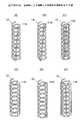
図2(A)乃至(F)は、本発明による接触子の実施例の変形例を示す。
図2(A)に於いては、導電部材11Aの両端が、コイル状スプリング12に溶接される。図2(B)に於いては、導電部材11Bの両端が、コイル状スプリング12に引っかけて固定される。図2(C)に於いては、複数の導電部材11Cが設けられ、その両端がコイル状スプリング12に溶接される。図2(D)に於いては、導電部材11Dがコイル状スプリング12の外部に配置され、その両端がコイル状スプリング12に溶接される。図2(E)に於いては、導電部材11Eがコイル状スプリング12の外部に配置され、その両端がコイル状スプリング12に引っかけて固定される。図2(F)に於いては、複数の導電部材11Fがコイル状スプリング12の外部に配置され、その両端がコイル状スプリング12に溶接される。
【0030】
このように、図1の接触子と同一の機能は、様々な変形例によって実施することが可能である。特に図2(C)或いは(F)のように、複数の導電部材が設けられる構成に於いては、一本の導電部材の場合に比較して、電流伝達経路の抵抗及びインダクタンスを更に小さくすることが出来る。
図3(A)及び(B)は、本発明による電気的接続装置の実施例を示す図である。
【0031】
図3(A)に示されるように、本発明による電気的接続装置は、本発明による接触子10、ガイド板20、ねじ22、ねじ止め23、及び基板24を含む。ガイド板20には複数の穴21が、半導体装置30の外部電極31に位置に対応して設けられ、接触子10が穴21内部に挿入される。ガイド板20は、ねじ22及びねじ止め23によって、基板24に固定される。
【0032】
図3(B)は、図3(A)に示される電気的接続装置に於いて、部分Aを拡大して示す部分拡大図である。図3(B)に示されるように、接触子10はランドパターン25に接するように、ガイド板20の穴21内に配置される。ここで穴21は、図に示されるように例えば中央部で内径の狭まったテーパ状になっており、接触子10が抜け落ちることを防ぐ。ランドパターン25には配線26が設けられており、試験装置(図示せず)と接続される。
【0033】
上記実施例の電気的接続装置によれば、半導体装置30等の外部電極31と、安定した良好な電気的接続を行うことが可能であり、試験装置によって半導体装置30等の試験を容易に行うことが可能になる。また接触子10及びガイド板20の構造は比較的単純であるために、微細化することが容易であり、微細ピッチで外部電極31が配置された半導体装置30に対しても十分に対応することが出来る。
【0034】
図4は、本発明による電気的接続装置の別の実施例を示す。図4に於いて、図3と同一の要素は同一の番号で参照され、その説明は省略される。
図4の実施例に於いては、接触子10の代わりに接触子10Aが用いられる。接触子10Aは、ランドパターン25側の端部が金属圧着部11bとして、ランドパターン25に圧着される。圧着としては、例えば半田を用いて、金属ボール11aを溶解してランドパターン25に接続することが考えられる。
【0035】
図4に示す実施例に於いては、接触子10Aとランドパターン25とを圧着することで、電気的接続の信頼性を向上させることが出来る。
図5は、本発明による電気的接続装置の更なる別の実施例を示す。図5に於いて、図3と同一の要素は同一の番号で参照され、その説明は省略される。
図5の実施例に於いては、穴27を有する2枚のガイド板20A及び20Bが、重ね合わせて用いられる。重ね合わせる面の穴27の位置には、段差27aが設けられる。ガイド板20Aの段差27aとガイド板20Bの段差27aとが形成する空間内に、直列接続される接触子10Bの接続部分11cをはめ込むように配置する。この構成によって、接触子10Bの抜け落ちを防止することが出来る。
【0036】
図6は、本発明による電気的接続装置の更なる別の実施例を示す。図6に於いて、図5と同一の要素は同一の番号で参照され、その説明は省略される。
図6の実施例に於いては、穴27を有する2枚のガイド板20A及び20Bが、重ね合わせて用いられる。重ね合わせる面の穴27の位置には、段差27aが設けられる。ガイド板20Aの段差27aとガイド板20Bの段差27aとが形成する空間内に、中継部材13がはめ込まれる。直列接続される接触子10Bの接続部分11cが、中継部材13に接続される。この構成によって、接触子10Bの抜け落ちを防止することが出来る。
【0037】
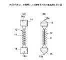
図7(A)及び(B)は、本発明による接触子の別の実施例を示す。図7(A)及び(B)に於いて、図1(A)及び(B)と同一の要素は同一の番号で参照され、その説明は省略される。
図7(A)の接触子は、導電部材11と、コイル状スプリング12と、導電部材11の両端に接続されるコンタクト用金属片14を含む。図7(A)のコンタクト用金属片14は、へこみ14aを有しており、へこみ14a内にBGA(Ball Grid Array )タイプの半導体装置等のボール状外部電極をはめ込むことで、確実な電気的接続を確立することが出来る。
図7(B)の接触子は、導電部材11と、コイル状スプリング12と、導電部材11の両端に接続されるコンタクト用金属片15を含む。図7(B)のコンタクト用金属片15は、尖った先端部15aを有しており、先端部15aをQFPタイプの半導体装置等のピン状外部電極や、図3(B)の基板24のランドパターン25のような電極に強く押しつけることで、確実な電気的接続を確立することが出来る。
【0038】
このように図7(A)及び(B)に示される接触子に於いては、接続する電極の形状に適したコンタクト用金属片を設けることで、確実な電気的接続を確立することが出来る。なお接触子の両端に同一形状のコンタクト用金属片を設ける必要はなく、例えば図7(A)のコンタクト用金属片14を一端に設け、図7(B)のコンタクト用金属片15を他端に設ける構成としてもよい。
【0039】
図8は、図7(A)及び(B)に示されるタイプの接触子を用いた接続の様子を示す図である。図8に於いて、図3(A)及び(B)並びに図7(A)及び(B)と同一の要素は同一の番号で参照され、その説明は省略される。
図8の接触子に於いては、コンタクト用金属片14が一端に設けられ、コンタクト用金属片15が他端に設けられる。またコンタクト用金属片14のへこみ14aとコンタクト用金属片15の先端部15aには、電気的接続を向上させるためにAu等の金属メッキ16が施される。
【0040】
コンタクト用金属片14のへこみ14aには、半導体装置30のボール状外部電極31がはめ込まれ、コンタクト用金属片15の先端部15aは、基板24のランドパターン25に押しつけられる。これによって、半導体装置30のボール状外部電極31とランドパターン25との間で確実な電気的接続を行うことが出来る。
【0041】
図9(A)乃至(D)は、図1(A)に示される接触子10を製造する製造方法を示す図である。
図9(A)に示されるように、ワイヤーリール40からワイヤー42が引き出され、押さえ治具41に固定されるコイル状スプリング12内に挿入される。図9(B)は、ワイヤー42がコイル状スプリング12内に挿入された状態を示す。この状態で、図9(C)に示すように、例えば水素トーチ法によって、コイル状スプリング12の両端でワイヤー42を熱切断する。ワイヤー42が熱切断されると、切断端でワイヤー42が球状に固まり、図9(D)に示されるようにコイル状スプリング12の内部に挿入された導電部材11とその両端の金属ボール11aが構成される。
【0042】
図9(C)に於いては、水素トーチ法によってワイヤー42を熱切断したが、例えば電気放電処理により、ワイヤー42を熱切断してもよい。
このように本発明による接触子10は、単純な工程によって容易に製造することが可能であり、大量生産に適している。
図10は、本発明による電気的接続装置を用いた半導体装置試験システムの構成を示す図である。
【0043】
図10の半導体装置試験システムは、テスター50、テストヘッド部51、テストヘッド部51とテスタ50とを接続する配線52、テストヘッド部51に設けられた本発明による電気的接続装置を用いたコンタクタ部53を含む。コンタクタ部53にはLSI60がはめ込まれ、テスター50によってLSI60の試験を行う。図10の半導体装置試験システムは、例えば図3(A)に示す本発明による電気的接続装置を用いる以外は、従来技術の範囲内であるので詳細な説明は省略する。
【0044】
図11(A)乃至(C)は、図10の半導体装置試験システムによる半導体装置試験工程を示す図である。図11(A)乃至(C)に於いて、図3(A)及び(B)並びに図10と同一の要素は同一の番号で参照され、その説明は省略される。図11(A)に示されるように、コンタクタ部53は、LSI60の外部電極61の配置に対応して、本発明による接触子10を配列したガイド板20を含む。LSI60が、コンタクタ部53内部に挿入されて、外部電極61と接触子10との電気的接続が確立される。図11(B)は、LSI60が、コンタクタ部53内部に挿入された状態を示し、この状態で、LSI60に対する種々の電気的試験が実施される。試験終了後に、図11(C)に示されるように、LSI60がコンタクト部43から取り除かれる。
【0045】
このように、本発明による電気的接続装置を備えた図10に示す半導体試験システムを用いて、図11(A)乃至(C)に示される工程で半導体装置の試験を行えば、容易に半導体装置の装着・取り外しを行いながらも、安定した良好な電気的接続条件のもとで半導体装置試験を実行することが可能になる。
以上、本発明を実施例に基づいて説明したが、本発明は上述の実施例に限定されるものではなく、特許請求の範囲に記載される範囲内で、自由に変形・変更が可能である。
【0046】
【発明の効果】
請求項1の発明に於ては、第1の電極と第2の電極との間の電気的接続を、コイル状スプリングではなく導電部材を介して行うことで、電流の伝達経路を短くして低抵抗かつ低インダクタンスの安定した電気伝達特性を実現すると共に、コイル状スプリングにより接触圧を生成することが可能となる。また安定した良好な電気伝達特性を実現することで、電気信号の劣化を防ぐことが出来る。
【0047】
請求項2の発明に於ては、導電部材の端部の大きさをコイル状スプリングの内径よりも大きくすることで、導電部材がコイル状スプリングから抜け落ちるのを防ぐことが出来る。
請求項3の発明に於ては、コイル状スプリングの伸縮方向に延在する導電部材の端部をコイル状スプリングの両端に接続することで、導電部材がコイル状スプリングから抜け落ちるのを防ぐことが出来る。
【0048】
請求項4の発明に於ては、コイル状スプリングの伸縮方向に延在する導電部材の端部をコイル状スプリングの両端に接続することで、導電部材がコイル状スプリングから分離するのを防ぐことが出来る。
請求項5の発明に於ては、複数の導電部材を並列に配置することで、単一の導電部材を用いる場合に比較して、導電部材の抵抗を更に小さくすることが出来る。
【0049】
請求項6の発明に於ては、導電部材の両端にコンタクト用金属片を設けることで、安定した電気接続のためのコンタクトを確立することが出来る。
請求項7の発明に於ては、ボール状電極をはめ込むためのくぼみをコンタクト用金属片に設けることで、ボール状電極に対する安定したコンタクトを確立することが出来る。
【0050】
請求項8の発明に於ては、電極に押しつけるための尖鋭先端部をコンタクト用金属片に設けることで、ピン状電極等に対する安定したコンタクトを確立することが出来る。
請求項9の発明に於ては、導電性の高い金属メッキ層を介して電気接続を行うことで、安定した電気接続を行うことが出来る。
【0051】
請求項10の発明に於ては、第1の電極と第2の電極との間の電気的接続を、コイル状スプリングではなく導電部材を介して行うことで、電流の伝達経路を短くして低抵抗かつ低インダクタンスの安定した電気伝達特性を実現すると共に、コイル状スプリングにより接触圧を生成することが可能となる。また微細なピッチで多数のピンが配列された半導体装置に対しても、対応した微細ピッチで貫通穴を配置して接触子を挿入することは容易であり、安価で高性能の電気的接続装置を提供することが出来る。
【0052】
請求項11の発明に於ては、貫通穴をテーパ状に形成することで、接触子が貫通穴から抜け落ちるのを防ぐことが出来る。
請求項12の発明に於ては、貫通穴内で複数の接触子を直列に配置することで、ガイド板により接触子を支持することが容易になる。
請求項13の発明に於ては、ガイド板によって接触子を支持することで、接触子が貫通穴から抜け落ちるのを防ぐことが出来る。
【0053】
請求項14の発明に於ては、ガイド板によって中継部材を支持することで、接触子が貫通穴から抜け落ちるのを防ぐことが出来る。
請求項15の発明に於ては、接触子を基板に圧着実装することによって、基板との電気的接続性を向上することが出来る。
請求項16の発明に於ては、単純な工程で接触子を製造することが可能であり、接触子を低いコストで大量に製造することが出来る。
【0054】
請求項17の発明に於ては、導電部材を介して安定した良好な電気伝達特性を提供することが出来るので、電気信号の劣化を防いだ精度の高い半導体装置試験を実施することが可能になる。
【図面の簡単な説明】
【図1】(A)及び(B)は、本発明による接触子の実施例を示す図である。
【図2】(A)乃至(F)は、本発明による接触子の実施例の変形例を示す図である。
【図3】(A)及び(B)は、本発明による電気的接続装置の実施例を示す図である。
【図4】本発明による電気的接続装置の別の実施例を示す図である。
【図5】本発明による電気的接続装置の更なる別の実施例を示す図である。
【図6】本発明による電気的接続装置の更なる別の実施例を示す図である。
【図7】(A)及び(B)は、本発明による接触子の別の実施例を示す図である。
【図8】図7(A)及び(B)に示されるタイプの接触子を用いた接続の様子を示す図である。
【図9】(A)乃至(D)は、図1(A)に示される接触子を製造する製造方法を示す図である。
【図10】本発明による電気的接続装置を用いた半導体装置試験システムの構成を示す図である。
【図11】(A)乃至(C)は、図10の半導体装置試験システムによる半導体装置試験工程を示す図である。
【図12】従来のプローブピンの構成を示す図である。
【図13】従来のプローブピンの別の構成を示す図である。
【符号の説明】
10 接触子
11 導電部材
11a 金属ボール
12 コイル状スプリング
20 ガイド板
21 穴
22 ねじ
23 ねじ止め
24 基板
30 半導体装置
31 外部電極
40 ワイヤーリール
41 押さえ治具
42 ワイヤー
50 テスター
51 テストヘッド部
52 配線
53 コンタクタ部
60 LSI
61 外部電極[0001]
BACKGROUND OF THE INVENTION
The present invention generally relates to an electrical connection mechanism for semiconductor devices and other electrical components, and more particularly, an IC package in which a large number of pins are arranged at a fine pitch, a high-speed / high-frequency IC such as a bare chip or a wafer, and other electrical components. The present invention relates to a connection device that performs an electrical connection to the like.
[0002]
[Prior art]
Conventionally, a contact such as a probe pin is generally used as a device for making an electrical connection to a semiconductor device or other electrical components.
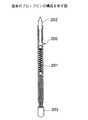
FIG. 12 is a diagram showing a configuration of a conventional probe pin. The probe pin of FIG. 12 includes a
[0003]
In the probe pin of FIG. 12, when the
[0004]
Therefore, recently, a probe pin as shown in FIG. 13 tends to be used. The probe pin of FIG. 13 includes a guide plate 210, a plurality of
[0005]
[Problems to be solved by the invention]
In the probe pin configured as shown in FIG. 13, current is transmitted through the
[0006]
As shown in FIG. 13, when the structure in which a part of the
[0007]
Accordingly, an object of the present invention is to provide a contact and an electrical connection device having stable and good current transfer characteristics.
[0008]
[Means for Solving the Problems]
In the first aspect of the present invention, the electrical connection device includes a coil spring and an extension direction of the coil spring.Deform when the coiled spring shrinks When the conductive member includes a deformable conductive member and one end of the conductive member is in contact with the first electrode and the other end is in contact with the second electrode, the first electrode and the second electrode are interposed via the conductive member. In addition to being electrically connected to the electrode, the coiled spring is contracted to generate a pressure of contact with the first electrode and the second electrode.
[0009]
In the above invention, the electrical connection between the first electrode and the second electrode is performed not through the coiled spring but through the conductive member. A stable electrical transmission characteristic with low inductance can be realized, and a contact pressure can be generated by a coil spring. In addition, by realizing stable and good electrical transmission characteristics, it is possible to prevent deterioration of electrical signals.
[0010]
According to a second aspect of the present invention, in the electrical connection device according to the first aspect, the conductive member extends in the expansion and contraction direction of the coiled spring within the diameter of the coiled spring, and the coiled It has an end portion larger than the inner diameter of the spring.
In the above invention, the size of the end portion of the conductive member is made larger than the inner diameter of the coil spring, so that the conductive member can be prevented from falling off the coil spring.
[0011]
According to a third aspect of the present invention, in the electrical connection device according to the first aspect, the conductive member extends in the expansion and contraction direction of the coiled spring within the diameter of the coiled spring, and the coiled It has the edge part connected to the both ends of a spring, It is characterized by the above-mentioned.
In the above-mentioned invention, it is possible to prevent the conductive member from falling out of the coiled spring by connecting the ends of the conductive member extending in the expansion / contraction direction of the coiled spring to both ends of the coiled spring.
[0012]
According to a fourth aspect of the present invention, in the electrical connecting device according to the first aspect, the conductive member extends outside the diameter of the coil spring and extends in the expansion and contraction direction of the coil spring. It has the edge part connected to the both ends of a spring, It is characterized by the above-mentioned.
In the said invention, it can prevent that a conductive member isolate | separates from a coiled spring by connecting the edge part of the conductive member extended in the expansion-contraction direction of a coiled spring to the both ends of a coiled spring.
[0013]
According to a fifth aspect of the present invention, in the electrical connecting device according to the first aspect, the conductive member includes a plurality of conductive members arranged in parallel.
In the above invention, by arranging a plurality of conductive members in parallel, the resistance of the conductive members can be further reduced as compared with the case where a single conductive member is used.
According to a sixth aspect of the present invention, there is provided the electrical connection device according to the first aspect, wherein both ends of the conductive member are provided to establish an electrical connection between the first electrode and the second electrode. It further includes a provided metal piece for contact.
[0014]
In the above-mentioned invention, a contact for stable electrical connection can be established by providing contact metal pieces on both ends of the conductive member.
According to a seventh aspect of the present invention, in the electrical connecting device according to the sixth aspect, the contact metal piece has a recess for fitting the protruding electrode.
[0015]
In the above invention, a stable contact with the ball-shaped electrode can be established by providing the contact metal piece with a recess for fitting the ball-shaped electrode.
According to an eighth aspect of the present invention, in the electrical connecting device according to the sixth aspect, the contact metal piece has a sharp tip for pressing against the electrode.
[0016]
In the above-mentioned invention, a stable contact with the pin-shaped electrode or the like can be established by providing the pointed tip for pressing against the electrode on the contact metal piece.
According to a ninth aspect of the present invention, in the electrical connection device according to the first aspect, the method further includes a conductive metal plating layer provided on at least one of the one end and the other end of the conductive member. It is characterized by.
[0017]
In the said invention, the stable electrical connection can be performed by performing electrical connection through a highly electroconductive metal plating layer. According to a tenth aspect of the present invention, the electrical connection device includes a coiled spring and an extension / contraction direction of the coiled spring.Deform when the coiled spring shrinks When the conductive member includes a deformable conductive member and one end of the conductive member is in contact with the first electrode and the other end is in contact with the second electrode, the first electrode and the second electrode are interposed via the conductive member. A plurality of contacts for electrically connecting the electrodes and generating a pressure of contact with the first electrode and the second electrode by contraction of the coiled spring; It includes a guide plate having through holes.
[0018]
In the above invention, the electrical connection between the first electrode and the second electrode is performed not through the coiled spring but through the conductive member. A stable electrical transmission characteristic with low inductance can be realized, and a contact pressure can be generated by a coil spring. In addition, even for semiconductor devices in which a large number of pins are arranged at a fine pitch, it is easy to place through-holes at a corresponding fine pitch and insert a contact, and this is an inexpensive and high-performance electrical connection device. Can be provided.
[0019]
According to an eleventh aspect of the present invention, in the electrical connecting device according to the tenth aspect, the through hole has an inner wall formed in a tapered shape.And prevents the contact from falling off due to the narrowed inner diameter. It is characterized by that. In the above invention, the contact hole can be prevented from falling out of the through hole by forming the through hole in a tapered shape. According to a twelfth aspect of the present invention, in the electrical connection device according to the tenth aspect, the plurality of contacts are arranged in series inside each of the plurality of through holes. To do.
[0020]
In the above invention, by arranging a plurality of contacts in series in the through hole, it becomes easy to support the contacts by the guide plate.
According to a thirteenth aspect of the present invention, in the electrical connection device according to the twelfth aspect, the plurality of through holes have step portions in the middle of the extension, and the plurality of contactors arranged in series. A connecting portion between each other is fitted into the stepped portion.
[0021]
In the above invention, the contact can be prevented from falling out of the through hole by supporting the contact with the guide plate.
According to a fourteenth aspect of the present invention, in the electrical connecting device according to the twelfth aspect, the plurality of through holes have step portions in the middle of the extension, and the plurality of contactors arranged in series. Are connected via a relay member fitted in the stepped portion.
[0022]
In the above invention, the relay member is supported by the guide plate, so that the contact can be prevented from falling out of the through hole.
According to a fifteenth aspect of the present invention, in the electrical connection device according to the tenth aspect of the present invention, the electric connection device further includes a substrate including the second electrode, and the other end of the contact is crimped to the second electrode. It is implemented.
[0023]
In the above invention, the electrical connection with the substrate can be improved by crimping and mounting the contact to the substrate.
In a sixteenth aspect of the present invention, the contactor manufacturing method includes fixing a coiled spring with a jig, passing a wire made of a conductive metal into the coiled spring diameter, and at both ends of the coiled spring. The method includes the steps of forming a conductive member having metal balls larger than the inner diameter of the coiled spring at both ends and inserted into the coiled spring by melting and cutting the wire.
[0024]
In the above-mentioned invention, it is possible to manufacture the contacts by a simple process, and it is possible to manufacture a large number of contacts at a low cost. According to a seventeenth aspect of the present invention, there is provided a test method for a semiconductor device in which a coil spring and an extension direction of the coil spring are extended.Deform when the coiled spring shrinks When one end of the conductive member including the deformable conductive member is in contact with the first electrode and the other end is in contact with the second electrode, the first electrode and the second electrode are interposed via the conductive member. And a plurality of through-holes into which the contacts are inserted, respectively, and a coil spring that contracts to generate a pressure of contact with the first electrode and the second electrode A semiconductor device having the first electrode is mounted on an electrical connection device including a guide plate having a guide plate, a test is performed on the semiconductor device through the second electrode, and the electrical connection device Each step of removing the semiconductor device is included.
[0025]
In the above invention, stable and good electric transmission characteristics can be provided through the conductive member, and therefore it becomes possible to carry out a highly accurate semiconductor device test in which deterioration of electric signals is prevented.
[0026]
DETAILED DESCRIPTION OF THE INVENTION
Embodiments of the present invention will be described below with reference to the accompanying drawings.
1A and 1B show an embodiment of a contact according to the present invention.
The
[0027]
The diameter of the
[0028]
Thus, in the embodiment of the contact according to the present invention, the
[0029]
2A to 2F show a modification of the embodiment of the contact according to the present invention.
In FIG. 2A, both ends of the
[0030]
Thus, the same function as the contact of FIG. 1 can be implemented by various modifications. Particularly in the configuration in which a plurality of conductive members are provided as shown in FIG. 2 (C) or (F), the resistance and inductance of the current transmission path are further reduced as compared with the case of a single conductive member. I can do it.
3 (A) and 3 (B) are diagrams showing an embodiment of an electrical connection device according to the present invention.
[0031]
As shown in FIG. 3A, the electrical connection device according to the present invention includes the
[0032]
FIG. 3B is an enlarged partial view showing the portion A in the electrical connection apparatus shown in FIG. As shown in FIG. 3B, the
[0033]
According to the electrical connection device of the above embodiment, stable and good electrical connection with the
[0034]
FIG. 4 shows another embodiment of the electrical connection device according to the present invention. 4, the same elements as those of FIG. 3 are referred to by the same numerals, and a description thereof will be omitted.
In the embodiment of FIG. 4, a
[0035]
In the embodiment shown in FIG. 4, the reliability of electrical connection can be improved by pressing the
FIG. 5 shows a further alternative embodiment of the electrical connection device according to the invention. 5, the same elements as those of FIG. 3 are referred to by the same numerals, and a description thereof will be omitted.
In the embodiment of FIG. 5, two
[0036]
FIG. 6 shows a further alternative embodiment of the electrical connection device according to the invention. In FIG. 6, the same elements as those of FIG. 5 are referred to by the same numerals, and a description thereof will be omitted.
In the embodiment of FIG. 6, two
[0037]
7A and 7B show another embodiment of the contact according to the present invention. 7A and 7B, the same elements as those in FIGS. 1A and 1B are referred to by the same numerals, and a description thereof will be omitted.
The contact shown in FIG. 7A includes a
The contact shown in FIG. 7B includes a
[0038]
In this way, in the contact shown in FIGS. 7A and 7B, a reliable electrical connection can be established by providing a contact metal piece suitable for the shape of the electrode to be connected. . It is not necessary to provide contact metal pieces of the same shape at both ends of the contact. For example, the
[0039]
FIG. 8 is a diagram showing a state of connection using the type of contact shown in FIGS. 7 (A) and 7 (B). In FIG. 8, the same elements as those in FIGS. 3A and 3B and FIGS. 7A and 7B are referred to by the same numerals, and a description thereof will be omitted.
In the contact shown in FIG. 8, a
[0040]
The ball-shaped
[0041]
9A to 9D are views showing a manufacturing method for manufacturing the
As shown in FIG. 9A, the
[0042]
In FIG. 9C, the
Thus, the
FIG. 10 is a diagram showing a configuration of a semiconductor device test system using the electrical connection device according to the present invention.
[0043]
The semiconductor device test system of FIG. 10 includes a tester 50, a test head unit 51, a wiring 52 for connecting the test head unit 51 and the tester 50, and a contactor using the electrical connection device according to the present invention provided in the test head unit 51.
[0044]
11A to 11C are diagrams showing a semiconductor device test process by the semiconductor device test system of FIG. 11A to 11C, the same elements as those in FIGS. 3A and 3B and FIG. 10 are referred to by the same numerals, and a description thereof will be omitted. As shown in FIG. 11A, the
[0045]
As described above, the semiconductor device can be easily tested by testing the semiconductor device in the steps shown in FIGS. 11A to 11C using the semiconductor test system shown in FIG. It is possible to perform a semiconductor device test under stable and good electrical connection conditions while mounting / removing the device.
The present invention has been described based on the embodiments. However, the present invention is not limited to the above-described embodiments, and can be freely modified and changed within the scope described in the claims. .
[0046]
【The invention's effect】
In the first aspect of the present invention, the electrical connection between the first electrode and the second electrode is performed not through the coiled spring but through the conductive member, thereby shortening the current transmission path. A stable electric transmission characteristic with low resistance and low inductance is realized, and a contact pressure can be generated by a coiled spring. In addition, by realizing stable and good electrical transmission characteristics, it is possible to prevent deterioration of electrical signals.
[0047]
In the invention of claim 2, by making the size of the end of the conductive member larger than the inner diameter of the coiled spring, it is possible to prevent the conductive member from falling off the coiled spring.
According to the third aspect of the present invention, it is possible to prevent the conductive member from falling off the coiled spring by connecting the ends of the conductive member extending in the expansion / contraction direction of the coiled spring to both ends of the coiled spring. I can do it.
[0048]
In the invention of claim 4, the end of the conductive member extending in the expansion / contraction direction of the coil spring is connected to both ends of the coil spring to prevent the conductive member from being separated from the coil spring. I can do it.
In the invention of claim 5, by arranging a plurality of conductive members in parallel, the resistance of the conductive members can be further reduced as compared with the case of using a single conductive member.
[0049]
According to the sixth aspect of the present invention, a contact for stable electrical connection can be established by providing contact metal pieces on both ends of the conductive member.
In the seventh aspect of the present invention, a stable contact with the ball-shaped electrode can be established by providing the contact metal piece with a recess for fitting the ball-shaped electrode.
[0050]
In the eighth aspect of the invention, by providing the contact metal piece with a sharp tip for pressing against the electrode, a stable contact with the pin electrode or the like can be established.
According to the ninth aspect of the present invention, stable electrical connection can be performed by performing electrical connection through a highly conductive metal plating layer.
[0051]
In the tenth aspect of the invention, the electrical connection between the first electrode and the second electrode is performed not through the coiled spring but through the conductive member, thereby shortening the current transmission path. A stable electric transmission characteristic with low resistance and low inductance is realized, and a contact pressure can be generated by a coiled spring. In addition, even for semiconductor devices in which a large number of pins are arranged at a fine pitch, it is easy to place through-holes at a corresponding fine pitch and insert a contact, and this is an inexpensive and high-performance electrical connection device. Can be provided.
[0052]
In the invention of
In the invention of
According to the thirteenth aspect of the present invention, the contact can be prevented from falling out of the through hole by supporting the contact with the guide plate.
[0053]
In the invention of
According to the fifteenth aspect of the present invention, the electrical connection with the substrate can be improved by crimping and mounting the contact to the substrate.
In the invention of
[0054]
In the invention of claim 17, since stable and good electric transmission characteristics can be provided through the conductive member, it is possible to carry out a highly accurate semiconductor device test in which deterioration of the electric signal is prevented. Become.
[Brief description of the drawings]
FIGS. 1A and 1B are diagrams showing an embodiment of a contact according to the present invention.
FIGS. 2A to 2F are views showing a modification of the embodiment of the contact according to the present invention. FIGS.
FIGS. 3A and 3B are diagrams showing an embodiment of an electrical connection device according to the present invention. FIGS.
FIG. 4 is a diagram showing another embodiment of the electrical connecting device according to the present invention.
FIG. 5 is a view showing still another embodiment of the electrical connecting apparatus according to the present invention.
FIG. 6 is a view showing still another embodiment of the electrical connecting apparatus according to the present invention.
FIGS. 7A and 7B are views showing another embodiment of the contact according to the present invention. FIGS.
FIG. 8 is a diagram showing a state of connection using a contact of the type shown in FIGS. 7A and 7B.
9A to 9D are views showing a manufacturing method for manufacturing the contact shown in FIG. 1A.
FIG. 10 is a diagram showing a configuration of a semiconductor device test system using an electrical connection device according to the present invention.
11A to 11C are diagrams showing a semiconductor device test process by the semiconductor device test system of FIG.
FIG. 12 is a diagram showing a configuration of a conventional probe pin.
FIG. 13 is a diagram showing another configuration of a conventional probe pin.
[Explanation of symbols]
10 Contact
11 Conductive members
11a metal ball
12 Coiled spring
20 Guide plate
21 holes
22 screws
23 Screwing
24 Substrate
30 Semiconductor device
31 External electrode
40 wire reel
41 Holding jig
42 wires
50 tester
51 Test head
52 Wiring
53 Contactor
60 LSI
61 External electrode
Claims (17)
Translated fromJapanese該コイル状スプリングの伸縮方向に延在し該コイル状スプリングが縮むときに変形する変形可能な導電部材
を含み、該導電部材の一端が第1の電極に接触され他端が第2の電極に接触されると、該導電部材を介して該第1の電極と該第2の電極とを電気的に接続すると共に、該コイル状スプリングが縮むことで該第1の電極及び該第2の電極に対する接触の圧力を生成することを特徴とする電気的接続装置。A coiled spring;
Includes a deformable conductivemember is deformed when said coil springs extend in the expansion and contraction direction of the coil springis contracted, the other end one end of the conductive member is in contact with the first electrode to the second electrode When contacted, the first electrode and the second electrode are electrically connected via the conductive member, and the coiled spring is contracted to contract the first electrode and the second electrode. An electrical connection device that generates a pressure of contact with the device.
該コイル状スプリングの伸縮方向に延在し該コイル状スプリングが縮むときに変形する変形可能な導電部材
を含み、該導電部材の一端が第1の電極に接触され他端が第2の電極に接触されると、該導電部材を介して該第1の電極と該第2の電極とを電気的に接続すると共に、該コイル状スプリングが縮むことで該第1の電極及び該第2の電極に対する接触の圧力を生成する接触子と、
各々に該接触子が挿入される複数の貫通穴を有するガイド板
を含むことを特徴とする電気的接続装置。A coiled spring;
Includes a deformable conductivemember is deformed when said coil springs extend in the expansion and contraction direction of the coil springis contracted, the other end one end of the conductive member is in contact with the first electrode to the second electrode When contacted, the first electrode and the second electrode are electrically connected via the conductive member, and the coiled spring is contracted to contract the first electrode and the second electrode. A contact for generating a pressure of contact against,
An electrical connection device comprising a guide plate having a plurality of through holes into which the contacts are inserted.
導電性の金属からなるワイヤーを該コイル状スプリング径内に通し、
該コイル状スプリングの両端で該ワイヤーを溶解切断することで、該コイル状スプリングの内径よりも大きな金属球を両端に有し該コイル状スプリング内に挿入された導電部材を形成する
各段階を含むことを特徴とする接触子製造方法。Fix the coil spring with a jig,
Pass a wire made of conductive metal into the coiled spring diameter,
Each step includes forming a conductive member having metal balls larger than the inner diameter of the coiled spring at both ends and being inserted into the coiled spring by melting and cutting the wire at both ends of the coiled spring. A contactor manufacturing method characterized by the above.
該第2の電極を介して該半導体装置に対する試験を実施し、
該電気的接続装置から該半導体装置を取り除く
各段階を含むことを特徴とする半導体装置の試験方法。The other end one end of the conductive member comprises a deformable conductive memberto deform when extend in the expansion and contraction direction of the coil spring and the coil springshrinks the coiled spring is brought into contact with the first electrode and the second The first electrode and the second electrode are electrically connected to each other through the conductive member and the coiled spring is contracted when the first electrode and the second electrode are contracted. A semiconductor device having the first electrode is mounted on an electrical connection device including a contact plate that generates a pressure of contact with the electrode and a plurality of through holes into which the contact is inserted. ,
Performing a test on the semiconductor device via the second electrode;
A test method for a semiconductor device, comprising: removing each of the semiconductor devices from the electrical connection device.
Priority Applications (4)
| Application Number | Priority Date | Filing Date | Title |
|---|---|---|---|
| JP32910697AJP4060919B2 (en) | 1997-11-28 | 1997-11-28 | Electrical connection device, contact manufacturing method, and semiconductor test method |
| US09/104,332US6033233A (en) | 1997-11-28 | 1998-06-25 | Electrical connecting device, and semiconductor device testing method |
| KR1019980029646AKR100302554B1 (en) | 1997-11-28 | 1998-07-23 | Electrical connection device, contact manufacturing method and semiconductor test method |
| US09/480,001US6624645B2 (en) | 1997-11-28 | 2000-01-10 | Semiconductor device testing method, using a spring-biased transformable conductive member electrode connection |
Applications Claiming Priority (1)
| Application Number | Priority Date | Filing Date | Title |
|---|---|---|---|
| JP32910697AJP4060919B2 (en) | 1997-11-28 | 1997-11-28 | Electrical connection device, contact manufacturing method, and semiconductor test method |
Publications (2)
| Publication Number | Publication Date |
|---|---|
| JPH11162270A JPH11162270A (en) | 1999-06-18 |
| JP4060919B2true JP4060919B2 (en) | 2008-03-12 |
Family
ID=18217686
Family Applications (1)
| Application Number | Title | Priority Date | Filing Date |
|---|---|---|---|
| JP32910697AExpired - Fee RelatedJP4060919B2 (en) | 1997-11-28 | 1997-11-28 | Electrical connection device, contact manufacturing method, and semiconductor test method |
Country Status (3)
| Country | Link |
|---|---|
| US (2) | US6033233A (en) |
| JP (1) | JP4060919B2 (en) |
| KR (1) | KR100302554B1 (en) |
Cited By (1)
| Publication number | Priority date | Publication date | Assignee | Title |
|---|---|---|---|---|
| CN110389240A (en)* | 2018-04-20 | 2019-10-29 | 株洲中车时代电气股份有限公司 | A kind of electricity endurance test chip tooling |
Families Citing this family (97)
| Publication number | Priority date | Publication date | Assignee | Title |
|---|---|---|---|---|
| JP3949256B2 (en)* | 1998-02-19 | 2007-07-25 | 富士通株式会社 | Semiconductor element test carrier, semiconductor element test method, and semiconductor element test apparatus |
| JP4239268B2 (en)* | 1999-01-12 | 2009-03-18 | 日新電機株式会社 | Conductor and gas insulated switchgear using this conductor |
| JP4414017B2 (en)* | 1999-05-25 | 2010-02-10 | モレックス インコーポレイテド | IC socket |
| JP2001189743A (en)* | 2000-01-04 | 2001-07-10 | Toshiba Corp | Communications system |
| JP3801830B2 (en)* | 2000-02-02 | 2006-07-26 | 株式会社エンプラス | Socket for electrical parts |
| EP1296145B1 (en)* | 2000-06-28 | 2007-04-11 | NHK Spring Co., Ltd. | Conductive contact |
| JP2002050425A (en)* | 2000-08-03 | 2002-02-15 | Ulvac Japan Ltd | Current conducting terminal and receiving side terminal |
| US7254889B1 (en)* | 2000-09-08 | 2007-08-14 | Gabe Cherian | Interconnection devices |
| ATE388505T1 (en)* | 2000-09-22 | 2008-03-15 | Shinetsu Polymer Co | SPRING ELEMENT, PRESSURE CLAMP CONNECTOR AND HOLDER WITH PROBE FOR ELECTROACOUSTIC COMPONENT |
| US6439894B1 (en)* | 2001-01-31 | 2002-08-27 | High Connection Density, Inc. | Contact assembly for land grid array interposer or electrical connector |
| JP2002246098A (en)* | 2001-02-19 | 2002-08-30 | Usui Internatl Ind Co Ltd | Current introducing terminal for feeding power to vacuum chamber |
| JP2002270321A (en)* | 2001-03-07 | 2002-09-20 | Advanex Inc | Socket for semiconductor package |
| JP2002270320A (en)* | 2001-03-12 | 2002-09-20 | Advanex Inc | Socket for semiconductor package |
| US6695623B2 (en)* | 2001-05-31 | 2004-02-24 | International Business Machines Corporation | Enhanced electrical/mechanical connection for electronic devices |
| US7045889B2 (en)* | 2001-08-21 | 2006-05-16 | Micron Technology, Inc. | Device for establishing non-permanent electrical connection between an integrated circuit device lead element and a substrate |
| US7049693B2 (en)* | 2001-08-29 | 2006-05-23 | Micron Technology, Inc. | Electrical contact array for substrate assemblies |
| WO2003043161A1 (en)* | 2001-11-15 | 2003-05-22 | Min Kyiu Sin | Charger for mobile telephone |
| US7126062B1 (en)* | 2002-01-17 | 2006-10-24 | Ardent Concepts, Inc. | Compliant electrical contact assembly |
| USRE41663E1 (en) | 2002-01-17 | 2010-09-14 | Ardent Concepts, Inc. | Compliant electrical contact assembly |
| US7019222B2 (en)* | 2002-01-17 | 2006-03-28 | Ardent Concepts, Inc. | Compliant electrical contact assembly |
| US6909056B2 (en)* | 2002-01-17 | 2005-06-21 | Ardent Concepts, Inc. | Compliant electrical contact assembly |
| CA2473726A1 (en)* | 2002-01-17 | 2003-07-31 | Ardent Concepts, Inc. | Compliant electrical contact |
| US6860766B2 (en)* | 2002-03-08 | 2005-03-01 | Cinch Connectors, Inc. | Electrical connector |
| US6870251B2 (en)* | 2002-05-29 | 2005-03-22 | Intel Corporation | High-power LGA socket |
| WO2004005944A1 (en)* | 2002-07-05 | 2004-01-15 | Advantest Corporation | Contact, socket, socket board, and electronic component test apparatus |
| US6746252B1 (en)* | 2002-08-01 | 2004-06-08 | Plastronics Socket Partners, L.P. | High frequency compression mount receptacle with lineal contact members |
| US6823582B1 (en)* | 2002-08-02 | 2004-11-30 | National Semiconductor Corporation | Apparatus and method for force mounting semiconductor packages to printed circuit boards |
| TWI292196B (en)* | 2002-09-30 | 2008-01-01 | Via Tech Inc | Flip chip test structure |
| JP2004152536A (en)* | 2002-10-29 | 2004-05-27 | Otax Co Ltd | Socket for electronic component |
| US6801733B2 (en)* | 2003-01-21 | 2004-10-05 | Static Control Components, Inc. | Printer cartridge and method of making or refurbishing |
| US6846184B2 (en)* | 2003-01-24 | 2005-01-25 | High Connection Density Inc. | Low inductance electrical contacts and LGA connector system |
| JP3950799B2 (en)* | 2003-01-28 | 2007-08-01 | アルプス電気株式会社 | Connected device |
| JP4197659B2 (en)* | 2003-05-30 | 2008-12-17 | 富士通マイクロエレクトロニクス株式会社 | Contactor for electronic parts and test method using the same |
| JP4651965B2 (en)* | 2003-06-09 | 2011-03-16 | 株式会社リコー | Power storage chamber and apparatus having the power storage chamber |
| KR20050059417A (en) | 2003-12-12 | 2005-06-20 | 스미토모덴키고교가부시키가이샤 | Spiral terminal and method of manufacturing the same |
| KR100714599B1 (en)* | 2004-12-21 | 2007-05-07 | 삼성전기주식회사 | Built-in antenna assembly of wireless communication terminal |
| US7140884B2 (en) | 2005-01-26 | 2006-11-28 | International Business Machines Corporation | Contact assembly and method of making thereof |
| JP2006351327A (en)* | 2005-06-15 | 2006-12-28 | Alps Electric Co Ltd | Connection structure of members, its manufacturing method, and electronic equipment having connection structure of members |
| JP4792465B2 (en)* | 2005-08-09 | 2011-10-12 | 株式会社日本マイクロニクス | Probe for current test |
| JP4916719B2 (en)* | 2005-12-28 | 2012-04-18 | 日本発條株式会社 | Contact probe and contact probe mounting structure |
| US8102184B2 (en)* | 2006-01-17 | 2012-01-24 | Johnstech International | Test contact system for testing integrated circuits with packages having an array of signal and power contacts |
| US7463998B2 (en)* | 2006-02-23 | 2008-12-09 | University Of Southern California | Adaptive design of nanoscale electronic devices |
| EP1830620A1 (en)* | 2006-03-03 | 2007-09-05 | Lih Duo International Co., Ltd. | Elastomeric connector |
| TWM309110U (en)* | 2006-07-13 | 2007-04-01 | Lih Duo Int Co Ltd | Testing card for wafer quality |
| US7377822B1 (en)* | 2006-12-14 | 2008-05-27 | Lotes Co., Ltd. | Electrical connector |
| US7754972B2 (en)* | 2006-12-18 | 2010-07-13 | Illinois Tool Works Inc. | Grounded manifold and method for making the same |
| KR100907234B1 (en)* | 2007-06-12 | 2009-07-10 | 후지쯔 마이크로일렉트로닉스 가부시키가이샤 | Contactor member, contactor and contacting method |
| WO2009058858A1 (en)* | 2007-10-29 | 2009-05-07 | Ardent Concepts, Inc. | Compliant electrical contact and assembly |
| KR101013986B1 (en)* | 2008-06-30 | 2011-02-14 | 주식회사 아이에스시테크놀러지 | Test socket |
| KR101037786B1 (en)* | 2008-08-21 | 2011-05-27 | 주식회사 아이에스시테크놀러지 | Test socket with conductive wire inserted inside the spring and manufacturing method of the test socket |
| KR101019720B1 (en)* | 2008-10-24 | 2011-03-07 | 주식회사 아이에스시테크놀러지 | Test sockets in which the conductor can stick to the pad |
| US20100102841A1 (en)* | 2008-10-28 | 2010-04-29 | Ibiden Co., Ltd. | Device, method and probe for inspecting substrate |
| IT1395336B1 (en)* | 2009-01-20 | 2012-09-14 | Rise Technology S R L | ELASTIC CONTACT DEVICE FOR ELECTRONIC COMPONENTS WITH COLLASSANT COLUMNS |
| US8269516B1 (en)* | 2009-04-03 | 2012-09-18 | Xilinx, Inc. | High-speed contactor interconnect with circuitry |
| JP2011082482A (en)* | 2009-09-11 | 2011-04-21 | Fujitsu Ltd | Electronic device, method of manufacturing electronic device, and electronic equipment |
| US8427186B2 (en)* | 2010-01-12 | 2013-04-23 | Formfactor, Inc. | Probe element having a substantially zero stiffness and applications thereof |
| US8118604B2 (en)* | 2010-05-06 | 2012-02-21 | Hon Hai Precision Ind. Co., Ltd. | Socket connector having electrical element supported by insulated elastomer |
| US8562359B2 (en)* | 2011-01-18 | 2013-10-22 | Tyco Electronics Corporation | Electrical contact for interconnect member |
| JP2014508944A (en)* | 2011-03-21 | 2014-04-10 | ユニバーシティ・オブ・ウィンザー | Equipment for automatic testing / verification of electronic components |
| SG11201406561XA (en) | 2012-04-13 | 2014-11-27 | Capital Formation Inc | Test probe assembly and related methods |
| US9153890B2 (en)* | 2012-04-18 | 2015-10-06 | R+DCircuits, Inc. | Singulated elastomer electrical contactor for high performance interconnect systems and method for the same |
| US9059545B2 (en)* | 2012-07-11 | 2015-06-16 | Tyco Electronics Corporations | Socket connectors and methods of assembling socket connectors |
| US9831589B2 (en)* | 2012-10-03 | 2017-11-28 | Corad Technology Inc. | Compressible pin assembly having frictionlessly connected contact elements |
| US9570828B2 (en) | 2012-10-03 | 2017-02-14 | Corad Technology Inc. | Compressible pin assembly having frictionlessly connected contact elements |
| US20140094071A1 (en)* | 2012-10-03 | 2014-04-03 | Corad Technology Inc. | Compressible pin assembly having frictionlessly connected contact elements |
| US8956193B2 (en)* | 2012-12-12 | 2015-02-17 | Intel Corporation | Helicoil spring backing socket |
| KR102016427B1 (en)* | 2013-09-10 | 2019-09-02 | 삼성전자주식회사 | Pogo pin and probe card including the same |
| JP6489749B2 (en)* | 2014-03-17 | 2019-03-27 | コラド・テクノロジー・インコーポレーテッド | Compressible pin assembly with contact elements connected without friction |
| US9733304B2 (en)* | 2014-09-24 | 2017-08-15 | Micron Technology, Inc. | Semiconductor device test apparatuses |
| WO2017007200A2 (en)* | 2015-07-03 | 2017-01-12 | 주식회사 오킨스전자 | Test socket, test socket manufacturing method, and jig assembly for test socket |
| US9717148B2 (en)* | 2015-09-18 | 2017-07-25 | Quartzdyne, Inc. | Methods of forming a microelectronic device structure, and related microelectronic device structures and microelectronic devices |
| US10228391B2 (en)* | 2016-01-12 | 2019-03-12 | WinWay Tech. Co., Ltd. | Two-piece spring probe |
| CN106252295B (en)* | 2016-08-31 | 2018-12-07 | 国家电网公司 | Direct-current transmission converter valve cooling water channel and its electrode and metal electrode body |
| DE102016013412A1 (en) | 2016-11-10 | 2018-05-17 | Rosenberger Hochfrequenztechnik Gmbh & Co. Kg | Contact system and contact module |
| JP6760135B2 (en)* | 2017-03-02 | 2020-09-23 | オムロンヘルスケア株式会社 | Combination of low-frequency treatment device, main body for low-frequency treatment device, and pad and holder for low-frequency treatment device |
| FR3068781A1 (en) | 2017-07-06 | 2019-01-11 | Ateq | METHOD FOR DETECTING LEAKAGE OF HOLLOW PIECE AND INSTALLATION FOR IMPLEMENTING SUCH A METHOD |
| FR3073623B1 (en) | 2017-11-16 | 2019-11-08 | Ateq | INSTALLATION AND METHOD FOR DETECTING AND LOCATING A LEAK IN A FLUID TRANSPORT CIRCUIT, IN PARTICULAR AN AIRCRAFT |
| US11187752B2 (en)* | 2018-08-31 | 2021-11-30 | Ateq Corporation | Battery leak test device and methods |
| CN109404816B (en)* | 2018-09-21 | 2024-07-05 | 迪亚姆展示设备(昆山)有限公司 | Lamp bracket of display spotlight |
| US11973301B2 (en) | 2018-09-26 | 2024-04-30 | Microfabrica Inc. | Probes having improved mechanical and/or electrical properties for making contact between electronic circuit elements and methods for making |
| US12078657B2 (en) | 2019-12-31 | 2024-09-03 | Microfabrica Inc. | Compliant pin probes with extension springs, methods for making, and methods for using |
| US12181493B2 (en) | 2018-10-26 | 2024-12-31 | Microfabrica Inc. | Compliant probes including dual independently operable probe contact elements including at least one flat extension spring, methods for making, and methods for using |
| FR3092171B1 (en) | 2019-01-29 | 2021-04-30 | Ateq | Tracer gas leak detection system and corresponding use. |
| US12000865B2 (en) | 2019-02-14 | 2024-06-04 | Microfabrica Inc. | Multi-beam vertical probes with independent arms formed of a high conductivity metal for enhancing current carrying capacity and methods for making such probes |
| US11768227B1 (en) | 2019-02-22 | 2023-09-26 | Microfabrica Inc. | Multi-layer probes having longitudinal axes and preferential probe bending axes that lie in planes that are nominally parallel to planes of probe layers |
| EP3939708B1 (en)* | 2019-03-12 | 2023-11-08 | Alps Alpine Co., Ltd. | Electromagnetic drive device and operation device |
| US11322473B2 (en) | 2019-09-12 | 2022-05-03 | International Business Machines Corporation | Interconnect and tuning thereof |
| US11561243B2 (en) | 2019-09-12 | 2023-01-24 | International Business Machines Corporation | Compliant organic substrate assembly for rigid probes |
| US12196781B2 (en) | 2019-12-31 | 2025-01-14 | Microfabrica Inc. | Probes with planar unbiased spring elements for electronic component contact, methods for making such probes, and methods for using such probes |
| US11802891B1 (en) | 2019-12-31 | 2023-10-31 | Microfabrica Inc. | Compliant pin probes with multiple spring segments and compression spring deflection stabilization structures, methods for making, and methods for using |
| US12196782B2 (en) | 2019-12-31 | 2025-01-14 | Microfabrica Inc. | Probes with planar unbiased spring elements for electronic component contact, methods for making such probes, and methods for using such probes |
| US11761982B1 (en) | 2019-12-31 | 2023-09-19 | Microfabrica Inc. | Probes with planar unbiased spring elements for electronic component contact and methods for making such probes |
| FR3106661B1 (en) | 2020-01-28 | 2022-01-21 | Ateq | LEAK DETECTION DEVICE |
| US11774467B1 (en) | 2020-09-01 | 2023-10-03 | Microfabrica Inc. | Method of in situ modulation of structural material properties and/or template shape |
| US12146898B2 (en) | 2020-10-02 | 2024-11-19 | Microfabrica Inc. | Multi-beam probes with decoupled structural and current carrying beams and methods of making |
| KR102556869B1 (en)* | 2021-06-16 | 2023-07-18 | 주식회사 아이에스시 | Electrical connector |
| KR102722465B1 (en)* | 2022-05-24 | 2024-10-29 | 주식회사 아이에스시 | Connector for test |
Family Cites Families (16)
| Publication number | Priority date | Publication date | Assignee | Title |
|---|---|---|---|---|
| US4029375A (en)* | 1976-06-14 | 1977-06-14 | Electronic Engineering Company Of California | Miniature electrical connector |
| US4200351A (en)* | 1978-06-12 | 1980-04-29 | Everett/Charles, Inc. | Straight through electrical spring probe |
| US4199209A (en)* | 1978-08-18 | 1980-04-22 | Amp Incorporated | Electrical interconnecting device |
| US4528500A (en)* | 1980-11-25 | 1985-07-09 | Lightbody James D | Apparatus and method for testing circuit boards |
| US4841240A (en)* | 1988-01-29 | 1989-06-20 | American Telephone And Telegraph Company, At&T Bell Laboratories | Method and apparatus for verifying the continuity between a circuit board and a test fixture |
| US4904935A (en)* | 1988-11-14 | 1990-02-27 | Eaton Corporation | Electrical circuit board text fixture having movable platens |
| US5174763A (en)* | 1990-06-11 | 1992-12-29 | Itt Corporation | Contact assembly |
| US5371466A (en)* | 1992-07-29 | 1994-12-06 | The Regents Of The University Of California | MRI RF ground breaker assembly |
| EP0616394A1 (en)* | 1993-03-16 | 1994-09-21 | Hewlett-Packard Company | Method and system for producing electrically interconnected circuits |
| US5800184A (en)* | 1994-03-08 | 1998-09-01 | International Business Machines Corporation | High density electrical interconnect apparatus and method |
| JP3779346B2 (en)* | 1995-01-20 | 2006-05-24 | 日本発条株式会社 | LSI package socket |
| JP2648120B2 (en)* | 1995-02-08 | 1997-08-27 | 山一電機株式会社 | Surface contact type connector |
| US6046597A (en)* | 1995-10-04 | 2000-04-04 | Oz Technologies, Inc. | Test socket for an IC device |
| US5791914A (en)* | 1995-11-21 | 1998-08-11 | Loranger International Corporation | Electrical socket with floating guide plate |
| JPH1172534A (en)* | 1997-08-28 | 1999-03-16 | Mitsubishi Electric Corp | Semiconductor device with test terminal and IC socket |
| US6396293B1 (en)* | 1999-02-18 | 2002-05-28 | Delaware Capital Formation, Inc. | Self-closing spring probe |
- 1997
- 1997-11-28JPJP32910697Apatent/JP4060919B2/ennot_activeExpired - Fee Related
- 1998
- 1998-06-25USUS09/104,332patent/US6033233A/ennot_activeExpired - Lifetime
- 1998-07-23KRKR1019980029646Apatent/KR100302554B1/ennot_activeExpired - Fee Related
- 2000
- 2000-01-10USUS09/480,001patent/US6624645B2/ennot_activeExpired - Fee Related
Cited By (2)
| Publication number | Priority date | Publication date | Assignee | Title |
|---|---|---|---|---|
| CN110389240A (en)* | 2018-04-20 | 2019-10-29 | 株洲中车时代电气股份有限公司 | A kind of electricity endurance test chip tooling |
| CN110389240B (en)* | 2018-04-20 | 2020-11-20 | 株洲中车时代半导体有限公司 | Chip tool for electric endurance test |
Also Published As
| Publication number | Publication date |
|---|---|
| JPH11162270A (en) | 1999-06-18 |
| US20020060579A1 (en) | 2002-05-23 |
| KR19990044775A (en) | 1999-06-25 |
| US6624645B2 (en) | 2003-09-23 |
| US6033233A (en) | 2000-03-07 |
| KR100302554B1 (en) | 2001-11-22 |
Similar Documents
| Publication | Publication Date | Title |
|---|---|---|
| JP4060919B2 (en) | Electrical connection device, contact manufacturing method, and semiconductor test method | |
| US5973394A (en) | Small contactor for test probes, chip packaging and the like | |
| JP3414593B2 (en) | Conductive contact | |
| US7534654B2 (en) | Socket for making with electronic component, particularly semiconductor device with spring packaging, for fixturing, testing, burning-in or operating such a component | |
| KR100454546B1 (en) | Contact structure having silicon finger contactors and total stack-up structure using same | |
| EP1523229B1 (en) | Semiconductor exercising apparatus, test socket apparatus and method of making thereof | |
| US20010054906A1 (en) | Probe card and a method of manufacturing the same | |
| US6079987A (en) | Connector for electronic parts | |
| US7990168B2 (en) | Probe card including a sub-plate with a main supporter and a sub-supporter with the sub-supporter having probe needles | |
| JP2012501528A (en) | Test contact system for testing an integrated circuit having a package having an array of signal and power contacts | |
| JPH09184852A (en) | Conductive probe | |
| JP2008122403A (en) | Assembly method of wafer probe | |
| JP2004251884A (en) | Integrated circuit test probe | |
| JP3342789B2 (en) | Conductive contact | |
| JP4167202B2 (en) | Conductive contact | |
| JP2004333459A (en) | Contact probe, and semiconductor and electrical inspection device using the same | |
| JPH09219267A (en) | Bga-ic package testing contact socket | |
| KR100480665B1 (en) | Vertical Type Probe Device | |
| KR200328984Y1 (en) | Test socket for high frequency | |
| JP2001013166A (en) | Probe structure for semiconductor device evaluation and method of manufacturing the same | |
| CN111293448A (en) | Integrated spring needle with pressure welding structure | |
| JPH07326693A (en) | Contactor for bga package | |
| JP2002164137A (en) | Contact structure and is socket | |
| JP2024024262A (en) | electrical contacts | |
| JP2002131375A (en) | Semiconductor IC contact structure |
Legal Events
| Date | Code | Title | Description |
|---|---|---|---|
| A977 | Report on retrieval | Free format text:JAPANESE INTERMEDIATE CODE: A971007 Effective date:20050201 | |
| A131 | Notification of reasons for refusal | Free format text:JAPANESE INTERMEDIATE CODE: A131 Effective date:20061121 | |
| A521 | Written amendment | Free format text:JAPANESE INTERMEDIATE CODE: A523 Effective date:20070119 | |
| TRDD | Decision of grant or rejection written | ||
| A01 | Written decision to grant a patent or to grant a registration (utility model) | Free format text:JAPANESE INTERMEDIATE CODE: A01 Effective date:20071218 | |
| A61 | First payment of annual fees (during grant procedure) | Free format text:JAPANESE INTERMEDIATE CODE: A61 Effective date:20071221 | |
| FPAY | Renewal fee payment (event date is renewal date of database) | Free format text:PAYMENT UNTIL: 20101228 Year of fee payment:3 | |
| R150 | Certificate of patent or registration of utility model | Free format text:JAPANESE INTERMEDIATE CODE: R150 | |
| S111 | Request for change of ownership or part of ownership | Free format text:JAPANESE INTERMEDIATE CODE: R313111 | |
| FPAY | Renewal fee payment (event date is renewal date of database) | Free format text:PAYMENT UNTIL: 20101228 Year of fee payment:3 | |
| R350 | Written notification of registration of transfer | Free format text:JAPANESE INTERMEDIATE CODE: R350 | |
| FPAY | Renewal fee payment (event date is renewal date of database) | Free format text:PAYMENT UNTIL: 20111228 Year of fee payment:4 | |
| FPAY | Renewal fee payment (event date is renewal date of database) | Free format text:PAYMENT UNTIL: 20111228 Year of fee payment:4 | |
| S531 | Written request for registration of change of domicile | Free format text:JAPANESE INTERMEDIATE CODE: R313531 | |
| S533 | Written request for registration of change of name | Free format text:JAPANESE INTERMEDIATE CODE: R313533 | |
| FPAY | Renewal fee payment (event date is renewal date of database) | Free format text:PAYMENT UNTIL: 20111228 Year of fee payment:4 | |
| R350 | Written notification of registration of transfer | Free format text:JAPANESE INTERMEDIATE CODE: R350 | |
| FPAY | Renewal fee payment (event date is renewal date of database) | Free format text:PAYMENT UNTIL: 20111228 Year of fee payment:4 | |
| FPAY | Renewal fee payment (event date is renewal date of database) | Free format text:PAYMENT UNTIL: 20121228 Year of fee payment:5 | |
| FPAY | Renewal fee payment (event date is renewal date of database) | Free format text:PAYMENT UNTIL: 20121228 Year of fee payment:5 | |
| FPAY | Renewal fee payment (event date is renewal date of database) | Free format text:PAYMENT UNTIL: 20131228 Year of fee payment:6 | |
| S111 | Request for change of ownership or part of ownership | Free format text:JAPANESE INTERMEDIATE CODE: R313111 | |
| R350 | Written notification of registration of transfer | Free format text:JAPANESE INTERMEDIATE CODE: R350 | |
| LAPS | Cancellation because of no payment of annual fees |