JP4057468B2 - Illumination device with light transmission mechanism - Google Patents
Illumination device with light transmission mechanismDownload PDFInfo
- Publication number
- JP4057468B2 JP4057468B2JP2003157684AJP2003157684AJP4057468B2JP 4057468 B2JP4057468 B2JP 4057468B2JP 2003157684 AJP2003157684 AJP 2003157684AJP 2003157684 AJP2003157684 AJP 2003157684AJP 4057468 B2JP4057468 B2JP 4057468B2
- Authority
- JP
- Japan
- Prior art keywords
- light
- optical
- modulated
- transmission mechanism
- transmission
- Prior art date
- Legal status (The legal status is an assumption and is not a legal conclusion. Google has not performed a legal analysis and makes no representation as to the accuracy of the status listed.)
- Expired - Fee Related
Links
Images


Classifications
- H—ELECTRICITY
- H04—ELECTRIC COMMUNICATION TECHNIQUE
- H04B—TRANSMISSION
- H04B10/00—Transmission systems employing electromagnetic waves other than radio-waves, e.g. infrared, visible or ultraviolet light, or employing corpuscular radiation, e.g. quantum communication
- H04B10/11—Arrangements specific to free-space transmission, i.e. transmission through air or vacuum
- H04B10/114—Indoor or close-range type systems
- H04B10/1141—One-way transmission
- H—ELECTRICITY
- H04—ELECTRIC COMMUNICATION TECHNIQUE
- H04B—TRANSMISSION
- H04B10/00—Transmission systems employing electromagnetic waves other than radio-waves, e.g. infrared, visible or ultraviolet light, or employing corpuscular radiation, e.g. quantum communication
- H04B10/11—Arrangements specific to free-space transmission, i.e. transmission through air or vacuum
- H04B10/114—Indoor or close-range type systems
- H04B10/116—Visible light communication
Landscapes
- Physics & Mathematics (AREA)
- Electromagnetism (AREA)
- Engineering & Computer Science (AREA)
- Computer Networks & Wireless Communication (AREA)
- Signal Processing (AREA)
- Optical Communication System (AREA)
- Circuit Arrangement For Electric Light Sources In General (AREA)
- Led Device Packages (AREA)
- Photo Coupler, Interrupter, Optical-To-Optical Conversion Devices (AREA)
Description
Translated fromJapanese【0001】
【発明の属する技術分野】
本発明は、発光素子とその光の波長を変換して様々な色を発光し得る蛍光体とを含む照明装置に関し、特に空間を介して光信号を伝達する光伝送機能を兼ね備えた照明装置に関する。
【0002】
【従来の技術】
空間光伝送機能を兼ね備えた照明装置の1例として、特許文献1の特開2002−290335号公報において空間光伝送装置が開示されている。この空間光伝送装置は、照明用光源である赤、緑、および青のLED(発光ダイオード)へ供給する電力波形を情報に応じて変調しながらその光源を点灯させる送信側装置と、この送信側装置からの照明光を受ける受光手段を介してその照明光から情報を復調する受信側装置とを含んでいる。
【0003】
このような空間光伝送装置によれば、送信側装置を天井に配置できるので光伝送の障害が少なく、さらに通信機能と照明機能とを共通化することによって通信と照明の機能を兼ねる設備を簡素化し得る。
【0004】
【特許文献1】
特開2002−290335号公報
【0005】
【発明が解決しようとする課題】
上述のような特許文献1の空間光伝送装置は、照明機能を兼ね備えるために、伝送用の光の光源として最低でも赤、緑、および青の3色を発光する複数のLEDを用いる必要がある。
【0006】
また、このように伝送光として可視帯の波長を用いる場合には、太陽光が存在する状況においてその太陽光が伝送用の各色光に対する背景ノイズ光となるので、光伝送において十分なS/N(信号対ノイズ)比を保つことができず、したがって十分な伝送速度を実現することができない。
【0007】
特許文献1においては、空間光伝送装置の3原色光に別々の信号情報を含めて伝送することによって、いわゆるWDM(Wavelength Division Multiplex:波長分割多重)通信が可能であることも示唆されている。しかしながら、赤色、緑色、および青色を発光するそれぞれのLEDの駆動電圧は、それらのLEDに含まれる半導体発光層のバンドギャップに依存する。すなわち、異なる色を発光するLEDを駆動するための駆動電圧は互いに顕著に異なり、LED毎に個別の電圧で動作するよう設計された異なる駆動回路を設ける必要が生じる。
【0008】
上述のような先行技術における状況に鑑み、本発明は、ただ1つの光源を含みかつS/N比が良好な光通信機構を備えた照明装置を提供することを目的とし、さらにはWDM通信において複数の光源を駆動するために実質的に同一の電圧で動作する駆動回路を含む光通信機構を備えた照明装置を提供することをも目的としている。
【0009】
【課題を解決するための手段】
本発明による光伝送機構を備えた照明装置は、情報に応じて変調電気信号を生じる送信側電気回路と、変調電気信号に応じて強度変調光を放射する光源と、その光源から放射された光が通過する第1種類と第2種類の光路とを含み、第1種類の光路を通る光は光源に基づく当初の波長を維持し、第2種類の光路を通る光の少なくとも一部を照明光に波長変換する蛍光体を含む光波長変換手段と、光源に基づく当初の波長を有する光を受光して再生変調電気信号に変換する光電変換手段と、再生変調電気信号から情報を再生する受信側電気回路とをさらに含むことを特徴としている。
【0010】
なお、光源としては、半導体発光ダイオードと半導体レーザのいずれかが好ましく利用され得る。光源からの強度変調光は、380nm以上で430nm以下の範囲内の波長を有していることが好ましい。
【0011】
照明装置は、第1種類の光路において光の少なくとも一部を散乱させる光拡散手段をさらに含むことが好ましい。光波長変換手段に含まれる蛍光体は、第2種類の光路において光の少なくとも一部を散乱させるようにも作用し得る。
【0012】
変調光の変調帯域と蛍光体の発光強度の減衰係数とは、[変調光の変調帯域(Hz)>1/蛍光体の発光強度の減衰係数(sec)]の関係を満たすことが好ましい。光源は、蛍光体を励起し得る異なる波長の光を放射する複数の発光源を含むことができる。光電変換手段として受光素子を利用することができ、その上には光源に基づく当初の波長を有する光のみを透過する光学膜が設けられ得る。
【0013】
【発明の実施の形態】
(実施形態1)
図1は本発明の実施形態1による光伝送機構を備えた照明装置を模式的なブロック図で示しており、図2は図1の照明装置によって伝送される信号を模式的に示すタイミングチャートである。なお、本願の図面において、同一の参照符号は同一部分または相当部分を表している。
【0014】
図1の照明装置においては、光伝送機能を備えた照明光学系105と送信用回路部112が部屋の天井部に配置されている。そして、この光伝送機能を備えた照明光学系105中の照明用光学部は、波長390nmで発光するGaN系発光ダイオード100と、この発光ダイオードから放射された光を拡散させるレンズ101と、その光を2分割するビームスプリッタ102とを含み、分割された一方の光は赤色(Y2O2S:Eu3+)、緑色(ZnS:Cu,Al)、および青色((Sr,Ca,Ba,Mg)10(PO4)6:Eu3+)の蛍光体が分散されたアクリル樹脂板103に照射される。そして、それらの蛍光体からの蛍光115の混色光が空間に放射されることによって白色照明が行われ得る。
【0015】
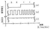
他方、光伝送機能を備えた照明光学系105中の伝送用の光学部では、ビームスプリッタ102で分割された他方の光が反射鏡117と透明アクリル樹脂板104を介して信号光116として空間に放射される。ここで、GaN系発光ダイオード100は、伝送速度10Mbps(Mbits/sec)の0と1からなる2値のデジタル伝送信号列108に基づいた出力と、環境温度の変動により生じる出力変動の補正と照明の光量を調整するためのバイアス供給回路107からの出力とが入力される変調回路106の出力によって駆動される。
【0016】
図2の模式的なタイミングチャートには、2値のデジタル電気信号列(a)、これに基づいて変調駆動されたGaN系発光ダイオードの光出力強度(b)、および蛍光体から放射される蛍光強度(c)が示されている。すなわち、図2中の横軸は1目盛りが0.1μsecの時間軸を表し、縦軸は電気信号レベルまたは光出力強度を表している。この図2から分かるように、GaN系発光ダイオードは伝送信号の周波数(10Mbps)に基づいて変調駆動されているが、蛍光体から放射される蛍光の強度の減衰係数は通常数μsec程度であるので、1ビットの信号伝送中の蛍光強度の変化は無視できる程度に小さい。また、この蛍光の強度変化は人間の目の光応答速度に対して十分に遅いので、目に感じるちらつきの問題をほとんど生じることがない。
【0017】
他方、部屋の任意の場所に設置されているPC(パソコン)や情報端末の1部分には、光伝送用の受信光学系111とそれに接続された受信用回路部114とが備えられている(図1参照)。この受信光学系111は、保護用の透明アクリル樹脂板110と、集光用レンズ101と、シリコン系の受光素子109を含んでいる。この受信光学系111によって、GaN系発光ダイオード100から空間に放射された光が受光素子109へ効率よく入射する。そして、この受光素子109によって光電変換された電気信号が復調回路112に入力されて、伝送信号113が復調される。ここで、復調回路112は、入力された信号を増幅するプリアンプ回路、信号の0と1を識別するコンパレータ回路、およびコンパレータ回路の信号を波形整形する波形整形回路を含んでいる。
【0018】
以上のように、蛍光体を励起する光源と伝送信号用の光源とを兼ねることが可能な光伝送機構を含む照明装置が実現され得る。そして、発光ダイオード100から蛍光体103を介して放射される蛍光115の照明領域とその蛍光体を介することなく放射される伝送信号光116の領域とがほぼ一致するので、その照明領域によって伝送領域を明らかにすることもできる。
【0019】
なお、本実施形態1における光学構成や回路構成などは、上述の例示に限られずに様々な形態をとることが可能である。また、本実施形態1においては送信部105、112と受信部111、114とが1対1で構成されているが、1対N(Nは複数の整数)やN対Nなどの配置を採用することも可能である。
【0020】
発光ダイオード100から放射される光の波長としては、太陽光による背景光ノイズを低減するために、太陽光スペクトルに存在しない波長である430nm以下で、かつ光伝送機構を備えた照明装置の各所に用いられるエポキシ樹脂の紫外線による黄色への変色を防止するために380nm以上であることが好ましい。
【0021】
(参考形態)
図3は、本発明に密接に関連する参考形態において利用される光伝送機能を備えた照明光学系105を模式的断面図で示している。すなわち、実施形態1に比べて参考形態の光伝送機構を備えた照明装置に特徴的なこととして、光源として発光ダイオードの代わりに半導体レーザ300を用いている。また、蛍光体が分散されているアクリル樹脂板103の厚さおよび/またはそのアクリル樹脂板中の蛍光体の分散状態において、光源300からのレーザ光の全てが蛍光板103に吸収されなくてその1部が空間に透過放射されるような厚さまたは分散状態に設定されている。
【0022】
このように、発光ダイオードに比べて素子容量により決まる時定数が小さくて数GHz以上の高速変調を行なうことが可能な半導体レーザ300を光源として用いることによって、高速の光伝送を行なうことができる。また、この蛍光板103中で吸収されずに透過した光を信号光116として利用することによって、実施形態1に比べて本参考形態の光学系の簡素化を図ることができる。
【0023】
ところで、空間的なコヒーレンス(可干渉性)を有する半導体レーザを光源として用いる場合には、空間に放射されるレーザ光に関して目に対する安全性の問題が懸念される。しかしながら、本参考形態におけるように蛍光板103に光を照射して、その蛍光体で吸収されずに空間に放射される光を信号光106として利用する場合には、蛍光板103内の蛍光体によってレーザ光が散乱されて空間的なコヒーレンスが低下するので、人間の目に対する安全性への問題を回避することができる。
【0024】
本参考形態の構成によって、実施形態1に比べてさらに高速伝送が可能な光伝送機構を含む照明装置が実現され得る。
【0025】
(実施形態2)
図4は、本発明の実施形態2において利用される光伝送機能を備えた照明光学系105を模式的断面図で示している。すなわち、実施形態1に比べて実施形態2の光伝送機構を含む照明装置に特徴的なこととして、照明光学系105において、発光ダイオードの代わりに半導体レーザ300を用いている。また、その半導体レーザから放射された光が照射される領域として、蛍光体が分散されている領域103と光を散乱させるTiO2粒子が分散された領域400とを含むアクリル樹脂板が設けられている。
【0026】
このような実施形態2においても、光学系の簡素化を図ることができる。また、半導体レーザ300から放射されたレーザ光の空間的なコヒーレンスは、TiO2粒子が分散された領域400によって低下させられ得る。さらに、本実施形態2によって、高速の伝送が可能な光伝送機構を含む照明装置を実現し得る。なお、非常に高い伝送速度を要しない場合には、半導体レーザ以外に発光ダイオードも光源として用いられ得ることは言うまでもない。
【0027】
(実施形態3)
図5と図6の模式的なタイミングチャートを参照して、本発明の実施形態3による光伝送機構を備えた照明装置における光伝送用の変調回路による変調方式が説明される。すなわち、本実施形態3では、光伝送信号の変調方法に関して、より好ましい方法が提供される。
【0028】
例えば、0と1からなる2値のデジタル伝送信号列では、確率的に伝送信号が0または1に偏ってしまう(続けて発生する)場合が発生し得る。また、デジタル伝送信号の伝送速度が非常に低速(例えば数100bps)の場合もあり得る。これらの場合には、蛍光体を励起する光の変調速度(Hz)が蛍光体の発光強度の減衰係数(sec)の逆数より小さいことに起因して蛍光のちらつきが発生してしまうので、照明装置においては不適当である。
【0029】
2値信号中の同じ信号が連続してしまうことを防ぐ手法として、伝送信号を任意のデータ数だけユニット化して、このユニット毎に信号列の配列に基づいた符号を付加するいわゆる符号化の処理が行なわれ得る(0が連続して続く場合や1が連続して続く場合に、1または0を付加するような処理)。この手法の具体例としては、例えば…0、0、0、0…の4つの伝送信号列に対して1を付加して…0、0、0、0、1…の信号列にする処理を行ない得る。
【0030】
しかしながら、このような対策によっても、蛍光のちらつきを完全には抑制することは困難であり、さらに、低速の伝送速度の場合に蛍光のちらつきを防ぐことができない。このような問題を解決すべく、本実施形態3の伝送方式による伝送信号列の一例が、図5に示されている。
【0031】
図5のタイミングチャートにおいて、横軸は1目盛りが0.1secの時間軸を表し、縦軸は信号電力または光出力を表している。図5に示されているように、10bpsの伝送速度における0と1の伝送電気信号列(a)に対応して、発光素子を駆動する駆動電流パルスの波高値が一定でデューティ比が50%となるパルス周波数を変化させた変調電気信号列(b)が用いられる。ここで、この変調信号列(b)の変調帯域(Hz)は、蛍光体の発光強度の減衰係数(sec)の逆数よりも大きくされる。
【0032】
なお、蛍光の減衰係数とは、初期の光強度を1とした場合に光強度が1/eに減少するまでの時間を意味する。一般的に、蛍光の減衰係数は数μsec程度であるので変調帯域はMHz以上に設定しておけばよい。
【0033】
このような本実施形態3においては、伝送信号列に0の信号列が続くような場合であっても、照明装置の蛍光強度(図5中の(c)参照)のちらつきを抑制することが可能な光伝送機構を含む照明装置を実現し得る。すなわち、実際の蛍光体による蛍光強度は図5中の光出力(c)の点線で表されるが、この点線の変動周波数は人間の目の応答速度に比べて十分速いので、実線で示された一定の蛍光強度として感じられる。さらに、このような変調信号列は、中速(数10kbps)の伝送に対しても効果を有し得る。そのような中速の伝送の例が、図6に図解されている。
【0034】
図6のタイミングチャートにおいて、横軸は1目盛りが0.1msecの時間軸を表し、縦軸は信号電力または光出力を表している。すなわち、図6において、10kbpsの伝送速度における0と1の伝送電気信号列(d)に基づいて、発光素子の入力が直接変調される。そして、その場合に蛍光体から放射される蛍光の光強度は、図6中の光出力(e)の点線で示される。しかし、この点線の変動周波数は人間の目の応答速度に比べて十分速いので、光出力(e)の実線で示された一定の蛍光強度として感じられる。
【0035】
このように、中速の伝送信号列の場合には、直接にその伝送信号列に基づいて光源が変調されても、蛍光体から放射される蛍光のちらつきを人間が感じることはない。しかしながら、実際の蛍光強度は光出力(e)の点線で示されているように変調されている。そして、伝送信号によって変調された信号光と蛍光体からの照明用蛍光が同時に受光素子に入射する場合には、その入射光強度は信号光の強度成分に蛍光強度の裾部の影響が重畳された光強度(f)となり、復調される伝送信号に対して蛍光強度の裾部がジッター成分となる。そして、このジッター成分がS/N比の低下の原因となる。
【0036】
これに対して、本実施形態3におけるように図5中の伝送信号列(b)により光源が変調される変調帯域(Hz)を蛍光体の発光強度の減衰係数(sec)の逆数より大きくなるように設定することによって、ジッター成分の影響を抑制することができる。
【0037】
なお、本実施形態3においては0と1からなる2値のデジタル信号について説明されたが、多値のデジタル信号やアナログ信号であれば、それに応じてパルス周期を多値またはアナログ的に変調することもできる。また、このパルスのディーティ比を適宜に変更する方式を採用してもよい。
【0038】
(実施形態4)
図7の模式的グラフは、本発明の実施形態4による光伝送機構を備えた照明装置の光学的特性を図解している。すなわち、実施形態1に比べて実施形態4の光伝送機構を含む照明装置に特徴的なこととして、光伝送用の受信光学系111に含まれるシリコン受光素子109上に(図1参照)、信号光116のみを透過させる光学特性を有する光学膜(図示せず)が形成されている。
【0039】
図7のグラフにおいて、横軸は光の波長(nm)を表し、左の縦軸は光強度(arb.:任意単位)を表し、そして右の縦軸は光学膜の反射率(%)を表している。また、図7中の曲線(a)は発光素子からの光の波長スペクトルを表し、曲線(b)は光学膜の光学特性(反射率)を表し、そして曲線(c)は蛍光体から放射される蛍光のスペクトルを表している。すなわち、この光学膜は、光源から放射される中心波長375nmの伝送信号に基づいて変調された光(a)のみを透過して、それ以外の波長の光を反射する光学特性(b)を有している。
【0040】
なお、このような光学特性を有する光学膜の設計手法においては、例えば酸化シリコン膜と窒化シリコン膜を含む多層膜構造が、膜中での光干渉の原理を利用して設定され得る。
【0041】
本実施形態4によれば、蛍光体から放射される赤、緑、青色などの可視光帯の照明光や背景光ノイズとなる太陽光が受光素子に入射することを防止し得る。このことによって、空間に放射された信号光のパワーとそれ以外の波長の光のパワーとの比によって決まるS/N比を良好にすることができ、高速の伝送が可能な光伝送機構を含む照明装置を実現し得る。
【0042】
(実施形態5)
図8は本発明の実施形態5による光伝送機構を備えた照明装置を模式的なブロック図で示しており、図9と図10はこの照明装置の光学的特性を模式的なグラフで示している。実施形態1に比べて本実施形態5において特徴的なこととして、420nm、425nm、および430nmの波長で発振する3つのGaN系半導体レーザを含む光源と、これらの半導体レーザを駆動する3つの回路が用いられている。なお、図8中においては、図面の簡略化のために、2つGaN系半導体レーザ300とそれらに接続された2対の回路部のみが示されている。
【0043】
図10のグラフにおいて、横軸は光の波長(nm)を表し、左の縦軸は蛍光体の吸収係数(%)を表し、そして右の縦軸は光強度(arb.)を表している。また、図10中で、光源となる3つのGaN系半導体レーザ300の発振スペクトルが破線の曲線(a)で表され、蛍光体の吸収スペクトルが実線の曲線(b)で示されている。図10に示されているように、各GaN系半導体レーザの発振波長は、用いられる蛍光体の吸収帯内に含まれるように選択されている。
【0044】
そして、図8に示されているように、各発振波長を有するGaN系半導体レーザ300は、実施形態1と同じ構成の伝送信号列108、バイアス供給回路107、および変調回路106によって個別に駆動される。これらのGaN系半導体レーザ300から放射されるレーザ光の1部は蛍光体が分散された媒質103に照射され、蛍光体から放射される蛍光115により照明が行われる。また、光拡散材が分散された媒質400で散乱された光は信号光116として空間に放射される。
【0045】
また、本実施形態5による光伝送用の受信光学系においては、3つの発振波長に対応して3つの受光素子設けられている。そして、ぞれぞれの受光素子上には、図9に示されているように、3つの波長420nm、425nm、および430nmのうちの1つのみが透過する帯域フィルタとなる光学膜が設けられている。すなわち、図9のグラフにおいて、横軸は光の波長(nm)を表し、左の縦軸は光強度(arb.)を表し、そして右の縦軸はフィルタの反射率(%)を表している。また、図9中の曲線(a)は半導体レーザの発光スペクトル分布を表し、曲線(b)は信号光に対する光学膜の反射特性を示している。
【0046】
このような本実施形態5によって、WDM(波長分割多重通信)方式の光伝送機構を備えた照明装置を実現し得る。また、この場合の複数の半導体レーザは、ほぼ同じ発振波長すなわちほぼ同一のエネルギーギャップを有しているので、ほぼ同じ駆動電圧で駆動することができ、半導体レーザ毎に駆動回路の動作電圧を変更する必要がない。
【0047】
なお、本実施形態5によるWDM方式の光伝送機構を備えた照明装置において用い得る発光素子としては、GaN系半導体レーザに限られず、GaN系発光ダイオードを使用することもできる。ただし、より多くの波長を用いて多重化する観点と、ノイズ成分光を光学膜で低減させてS/N比を良好に保つ観点とからは、発振スペクトル線幅の狭い半導体レーザを用いる方が好ましい。
【0048】
また、本実施形態5では個々の伝送信号列に基づいて個別にGaN系半導体レーザを駆動しているが、1つの伝送信号列をTDM(Time Divisions Multiplex:時分割多重)処理して、それぞれのGaN系発光ダイオードを時分割駆動することも可能である。
【0049】
【発明の効果】
以上のように、本発明によれば、光伝送と照明光とを1つの光源を用いて共通化することができるので、光伝送機能を備えた照明装置が簡略に実現し得る。また、本発明によれば、波長の異なる複数の発光素子を光源に利用することによって、WDM方式の光伝送機構を備えた照明装置を提供することもできる。
【図面の簡単な説明】
【図1】 本発明の一態様による光伝送機構を含む照明装置を模式的に示すブロック図である。
【図2】 図1の照明装置における伝送電気信号列(a)と、これに基づいて送信用の変調回路部で変調された光信号強度(b)と、蛍光体から放射される蛍光強度(c)とにおける時間変化を示すタイミングチャートである。
【図3】 本発明に密接に関連する参考形態おける光伝送用の光学部の形態を示す模式的断面図である。
【図4】 本発明における光伝送用の光学部の他の形態を示す模式断面図である。
【図5】 伝送電気信号列(a)と、これに基づいて送信用の変調回路部で変調された光信号強度(b)と、蛍光体から放射される蛍光強度(c)とにおける時間変化を示すタイミングチャートである。
【図6】 伝送電気信号列(d)と、蛍光体から放射される蛍光強度(e)と、受光素子に入射する信号光と蛍光が重畳された光強度(f)とにおける時間変化を示すタイミングチャートである。
【図7】 本発明の他の態様による光伝送用の受信光学系における光学特性を示す模式的グラフである。
【図8】 本発明の他の態様による光伝送機構を含む照明光学系を示す模式的ブロック図である。
【図9】 図8に示された光伝送用の受信光学系における光学特性を示す模式的グラフである。
【図10】 図8に示された光伝送機構を含む照明光学系における蛍光体の吸収特性と光源光の波長特性との関係を示す模式的グラフである。
【符号の説明】
100 発光ダイオード、101 拡散レンズ、102 ビームスプリッタ、103 蛍光体が分散されたアクリル樹脂、104 透明アクリル樹脂、105 光伝送機能を備えた照明光学系、106 変調回路、107 バイアス供給回路、108 伝送信号列、109 受光素子、110 透明アクリル樹脂、111 受信光学系、112 送信用電気回路部、113 再生伝送信号列、114 受信用電気回路部、115 照明用蛍光、116 信号光、117 反射鏡、300 半導体レーザ、400 拡散体(TiO2)が分散されたアクリル樹脂。[0001]
BACKGROUND OF THE INVENTION
The present invention relates to an illuminating device including a light emitting element and a phosphor capable of emitting various colors by converting the wavelength of the light, and particularly relates to an illuminating device having an optical transmission function of transmitting an optical signal through a space. .
[0002]
[Prior art]
As an example of a lighting device having a spatial light transmission function, Japanese Patent Application Laid-Open No. 2002-290335 discloses a spatial light transmission device. This spatial light transmission device includes a transmission-side device that lights a light source while modulating a power waveform supplied to red, green, and blue LEDs (light-emitting diodes), which are illumination light sources, according to information, and the transmission side. And a receiving side device for demodulating information from the illumination light via a light receiving means for receiving illumination light from the device.
[0003]
According to such a spatial light transmission device, since the transmission side device can be arranged on the ceiling, there are few obstacles in light transmission, and the communication function and the illumination function are made common, thereby simplifying the facility that functions as the communication and the illumination. Can be
[0004]
[Patent Document 1]
Japanese Patent Laid-Open No. 2002-290335
[Problems to be solved by the invention]
Since the spatial light transmission device of
[0006]
In addition, when a wavelength in the visible band is used as the transmission light in this way, since the sunlight becomes background noise light for each color light for transmission in a situation where sunlight exists, a sufficient S / N for optical transmission is obtained. The (signal to noise) ratio cannot be maintained, and therefore a sufficient transmission rate cannot be realized.
[0007]
[0008]
In view of the situation in the prior art as described above, an object of the present invention is to provide an illumination device including an optical communication mechanism that includes only one light source and has a good S / N ratio, and further in WDM communication. Another object of the present invention is to provide an illumination device including an optical communication mechanism including a drive circuit that operates at substantially the same voltage in order to drive a plurality of light sources.
[0009]
[Means for Solving the Problems]
An illumination device having an optical transmission mechanism according to the present invention includes a transmission-side electric circuit that generates a modulated electric signal according to information, a light source that emits intensity-modulated light according to the modulated electric signal, andlight emitted from the light source. The first type and the second type of optical path through which the light passes, the light passing through the first type of optical path maintains the original wavelength based on the light source, andat least part of the lightpassing through the second type of optical path is illumination light Optical wavelength conversion means including a phosphor forwavelength conversion, photoelectric conversion meansfor receiving lighthaving an initial wavelength based on thelight source and converting it to a reproduction modulated electric signal, and a receiving side for reproducing information from the reproduction modulated electric signal It is characterizedby further comprising an electric circuit.
[0010]
As the light source, either a semiconductor light emitting diode or a semiconductor laser can be preferably used. The intensity-modulated light from the light source preferably has a wavelength in the range of 380 nm to 430 nm.
[0011]
It is preferable that the illuminating device further includes a light diffusing unit that scatters at least a partof the light inthe first type optical path .The phosphorcontained in the light wavelength conversion means canalso act to scatter at least part of the light in the second type optical path .
[0012]
It is preferable that the modulation band of the modulated light and the attenuation coefficient of the emission intensity of the phosphor satisfy the relationship of [modulation band of the modulated light (Hz)> 1 / decay coefficient of the emission intensity of the phosphor (sec)]. The light source can include a plurality of light emitting sources that emit light of different wavelengths that can excite the phosphor. A light receiving element can be used as the photoelectric conversion means, and an optical film that transmits only lighthaving an initial wavelength based on the light source can be provided thereon.
[0013]
DETAILED DESCRIPTION OF THE INVENTION
(Embodiment 1)
FIG. 1 is a schematic block diagram showing a lighting device having an optical transmission mechanism according to
[0014]
In the illumination device of FIG. 1, an illumination
[0015]
On the other hand, in the optical unit for transmission in the illumination
[0016]
The schematic timing chart of FIG. 2 shows a binary digital electric signal string (a), the light output intensity (b) of a GaN-based light emitting diode modulated and driven based on this, and the fluorescence emitted from the phosphor. Intensity (c) is shown. That is, the horizontal axis in FIG. 2 represents the time axis with one scale of 0.1 μsec, and the vertical axis represents the electric signal level or the light output intensity. As can be seen from FIG. 2, the GaN-based light emitting diode is modulated and driven based on the frequency (10 Mbps) of the transmission signal, but the attenuation coefficient of the intensity of the fluorescence emitted from the phosphor is usually about several μsec. The change in fluorescence intensity during 1-bit signal transmission is negligibly small. In addition, since the change in the intensity of the fluorescence is sufficiently slow with respect to the light response speed of the human eye, there is almost no problem of flickering perceived by the eye.
[0017]
On the other hand, a part of a PC (personal computer) or information terminal installed in an arbitrary place in the room is provided with a receiving
[0018]
As described above, an illumination device including an optical transmission mechanism that can serve as both a light source that excites a phosphor and a light source for a transmission signal can be realized. Since the illumination region of the
[0019]
In addition, the optical configuration, the circuit configuration, and the like in the first embodiment are not limited to the above examples, and can take various forms. Further, in the first embodiment, the
[0020]
The wavelength of light emitted from the
[0021]
(Reference form)
FIG. 3 is a schematic cross-sectional view showing an illumination
[0022]
As described above, high-speed optical transmission can be performed by using the
[0023]
By the way, when a semiconductor laser having spatial coherence (coherence) is used as a light source, there is a concern about the safety of eyes with respect to laser light emitted into space. However, when irradiated with light to
[0024]
With the configuration of the presentembodiment , an illuminating device including an optical transmission mechanism capable of higher speed transmission than that of the first embodiment can be realized.
[0025]
(Embodiment2 )
FIG. 4 is a schematic cross-sectional view showing an illumination
[0026]
Also in thesecond embodiment, the optical system can be simplified. Further, the spatial coherence of the laser light emitted from the
[0027]
(Embodiment3 )
With reference to the schematic timing charts of FIG. 5 and FIG. 6, the modulation method by the light transmission modulation circuit in the illumination device having the light transmission mechanism according to thethird embodiment of the present invention will be described. That is, in thethird embodiment, a more preferable method is provided regarding the modulation method of the optical transmission signal.
[0028]
For example, in a binary digital transmission signal sequence composed of 0 and 1, there may occur a case where the transmission signal is probabilistically biased to 0 or 1 (occurs continuously). In addition, the transmission speed of the digital transmission signal may be very low (for example, several hundred bps). In these cases, the flickering of the fluorescence occurs due to the modulation rate (Hz) of the light that excites the phosphor being smaller than the reciprocal of the decay coefficient (sec) of the emission intensity of the phosphor. Inappropriate in the device.
[0029]
As a technique for preventing the same signal in the binary signal from continuing, a so-called encoding process in which the transmission signal is unitized by an arbitrary number of data and a code based on the arrangement of the signal sequence is added to each unit. (When 0 continues continuously or when 1 continues continuously, processing such as adding 1 or 0). As a specific example of this method, for example, a process is performed in which 1 is added to four transmission signal sequences of 0, 0, 0, 0 ... to make a signal sequence of 0, 0, 0, 0, 1 ... You can do it.
[0030]
However, even with such countermeasures, it is difficult to completely suppress the flickering of the fluorescence, and furthermore, it is not possible to prevent the flickering of the fluorescence when the transmission speed is low. In order to solve such a problem, an example of a transmission signal sequence according to the transmission system of thethird embodiment is shown in FIG.
[0031]
In the timing chart of FIG. 5, the horizontal axis represents a time axis with one scale of 0.1 sec, and the vertical axis represents signal power or optical output. As shown in FIG. 5, the peak value of the drive current pulse for driving the light emitting element is constant and the duty ratio is 50% corresponding to the transmission electric signal train (a) of 0 and 1 at a transmission rate of 10 bps. A modulated electric signal sequence (b) in which the pulse frequency is changed is used. Here, the modulation band (Hz) of the modulation signal sequence (b) is made larger than the reciprocal of the attenuation coefficient (sec) of the emission intensity of the phosphor.
[0032]
The fluorescence attenuation coefficient means the time until the light intensity decreases to 1 / e when the initial light intensity is 1. In general, since the fluorescence attenuation coefficient is about several μsec, the modulation band may be set to MHz or higher.
[0033]
In thethird embodiment, flickering of the fluorescence intensity of the illumination device (see (c) in FIG. 5) is suppressed even when the transmission signal sequence is followed by a 0 signal sequence. An illumination device including a possible light transmission mechanism can be realized. That is, the fluorescence intensity of the actual phosphor is represented by the dotted line of the light output (c) in FIG. 5, and the fluctuation frequency of this dotted line is sufficiently faster than the response speed of the human eye, and is represented by the solid line. It is felt as a constant fluorescence intensity. Furthermore, such a modulated signal sequence can be effective for medium-speed (several tens of kbps) transmission. An example of such a medium speed transmission is illustrated in FIG.
[0034]
In the timing chart of FIG. 6, the horizontal axis represents a time axis with one scale of 0.1 msec, and the vertical axis represents signal power or optical output. That is, in FIG. 6, the input of the light emitting element is directly modulated based on the transmission electric signal sequence (d) of 0 and 1 at a transmission rate of 10 kbps. In this case, the intensity of the fluorescence emitted from the phosphor is indicated by the dotted line of the light output (e) in FIG. However, since the fluctuation frequency of this dotted line is sufficiently faster than the response speed of the human eye, it can be felt as a constant fluorescence intensity indicated by the solid line of the light output (e).
[0035]
Thus, in the case of a medium-speed transmission signal sequence, even if the light source is directly modulated based on the transmission signal sequence, humans do not feel the flickering of the fluorescence emitted from the phosphor. However, the actual fluorescence intensity is modulated as indicated by the dotted line of light output (e). When the signal light modulated by the transmission signal and the fluorescent light for illumination from the phosphor enter the light receiving element at the same time, the intensity of the incident light is superimposed on the intensity component of the signal light by the influence of the tail of the fluorescence intensity. And the bottom of the fluorescence intensity becomes a jitter component with respect to the demodulated transmission signal. This jitter component causes a decrease in the S / N ratio.
[0036]
In contrast, as in thethird embodiment, the modulation band (Hz) in which the light source is modulated by the transmission signal sequence (b) in FIG. 5 is larger than the reciprocal of the attenuation coefficient (sec) of the emission intensity of the phosphor. By setting in this way, the influence of the jitter component can be suppressed.
[0037]
In thethird embodiment, a binary digital signal consisting of 0 and 1 has been described. However, in the case of a multi-value digital signal or an analog signal, the pulse period is modulated in a multi-value or analog manner accordingly. You can also. Further, a method of appropriately changing the duty ratio of this pulse may be adopted.
[0038]
(Embodiment4 )
The schematic graph of FIG. 7 illustrates the optical characteristics of a lighting device including an optical transmission mechanism according to Embodiment4 of the present invention. That is, as compared with the first embodiment, a characteristic of the illumination device including the light transmission mechanism of thefourth embodiment is that on the silicon
[0039]
In the graph of FIG. 7, the horizontal axis represents the wavelength of light (nm), the left vertical axis represents the light intensity (arb .: arbitrary unit), and the right vertical axis represents the reflectance (%) of the optical film. Represents. Also, curve (a) in FIG. 7 represents the wavelength spectrum of light from the light emitting element, curve (b) represents the optical characteristics (reflectance) of the optical film, and curve (c) is emitted from the phosphor. Represents the fluorescence spectrum. That is, this optical film has an optical characteristic (b) that transmits only light (a) modulated based on a transmission signal having a central wavelength of 375 nm emitted from a light source and reflects light of other wavelengths. is doing.
[0040]
In the design method of the optical film having such optical characteristics, for example, a multilayer film structure including a silicon oxide film and a silicon nitride film can be set using the principle of optical interference in the film.
[0041]
According to thefourth embodiment, it is possible to prevent illumination light in the visible light band such as red, green, and blue emitted from the phosphor and sunlight that becomes background light noise from entering the light receiving element. As a result, the S / N ratio determined by the ratio of the power of the signal light radiated to the space and the power of light of other wavelengths can be improved, and an optical transmission mechanism capable of high-speed transmission is included. An illumination device can be realized.
[0042]
(Embodiment5 )
FIG. 8 is a schematic block diagram showing an illuminating device provided with an optical transmission mechanism according to Embodiment5 of the present invention. FIGS. 9 and 10 are schematic graphs showing optical characteristics of the illuminating device. Yes. A characteristic of thefifth embodiment compared to the first embodiment is that a light source including three GaN-based semiconductor lasers that oscillate at wavelengths of 420 nm, 425 nm, and 430 nm, and three circuits that drive these semiconductor lasers. It is used. In FIG. 8, only two
[0043]
In the graph of FIG. 10, the horizontal axis represents the wavelength of light (nm), the left vertical axis represents the absorption coefficient (%) of the phosphor, and the right vertical axis represents the light intensity (arb.). . Further, in FIG. 10, the oscillation spectra of the three GaN-based
[0044]
As shown in FIG. 8, the GaN-based
[0045]
In the receiving optical system for optical transmission according to thefifth embodiment, three light receiving elements are provided corresponding to three oscillation wavelengths. On each of the light receiving elements, as shown in FIG. 9, an optical film serving as a bandpass filter that transmits only one of the three wavelengths 420 nm, 425 nm, and 430 nm is provided. ing. That is, in the graph of FIG. 9, the horizontal axis represents light wavelength (nm), the left vertical axis represents light intensity (arb.), And the right vertical axis represents filter reflectivity (%). Yes. Further, the curve (a) in FIG. 9 represents the emission spectrum distribution of the semiconductor laser, and the curve (b) represents the reflection characteristic of the optical film with respect to the signal light.
[0046]
According to thefifth embodiment, it is possible to realize an illuminating device including a WDM (wavelength division multiplexing) optical transmission mechanism. In addition, since the plurality of semiconductor lasers in this case have substantially the same oscillation wavelength, that is, almost the same energy gap, they can be driven with substantially the same drive voltage, and the operating voltage of the drive circuit is changed for each semiconductor laser. There is no need to do.
[0047]
Note that the light emitting element that can be used in the illumination device having the WDM optical transmission mechanism according to thefifth embodiment is not limited to the GaN semiconductor laser, and a GaN light emitting diode can also be used. However, from the viewpoint of multiplexing using more wavelengths and reducing the noise component light with an optical film and maintaining a good S / N ratio, it is better to use a semiconductor laser with a narrow oscillation spectrum line width. preferable.
[0048]
In thefifth embodiment, the GaN semiconductor lasers are individually driven based on the individual transmission signal sequences, but one transmission signal sequence is subjected to TDM (Time Divisions Multiplex) processing, It is also possible to drive the GaN-based light emitting diode in a time division manner.
[0049]
【The invention's effect】
As described above, according to the present invention, since light transmission and illumination light can be shared by using one light source, an illumination device having a light transmission function can be realized simply. In addition, according to the present invention, it is possible to provide an illumination device including a WDM optical transmission mechanism by using a plurality of light emitting elements having different wavelengths as light sources.
[Brief description of the drawings]
FIG. 1 is a block diagram schematically illustrating a lighting device including an optical transmission mechanism according to an aspect of the present invention.
2 shows a transmission electric signal sequence (a) in the illuminating device of FIG. 1, an optical signal intensity (b) modulated by a modulation circuit section for transmission based on this, and an intensity of fluorescence emitted from a phosphor ( It is a timing chart which shows the time change in c).
Figure 3 is a schematic sectional view showing aclosely related reference embodiment definitiveform stateof the optical part for light transmission to the present invention.
FIG. 4 is a schematic cross-sectional view showing another embodiment of the optical part for optical transmission in the present invention.
FIG. 5 shows temporal changes in a transmission electrical signal sequence (a), an optical signal intensity (b) modulated by a modulation circuit unit for transmission based on the transmission electric signal string (a), and a fluorescence intensity (c) emitted from a phosphor. It is a timing chart which shows.
FIG. 6 shows temporal changes in a transmission electric signal sequence (d), fluorescence intensity (e) emitted from a phosphor, and light intensity (f) in which signal light incident on a light receiving element and fluorescence are superimposed. It is a timing chart.
FIG. 7 is a schematic graph showing optical characteristics of a receiving optical system for optical transmission according to another embodiment of the present invention.
FIG. 8 is a schematic block diagram showing an illumination optical system including a light transmission mechanism according to another aspect of the present invention.
9 is a schematic graph showing optical characteristics in the optical transmission receiving optical system shown in FIG.
10 is a schematic graph showing the relationship between the absorption characteristic of the phosphor and the wavelength characteristic of the light source light in the illumination optical system including the light transmission mechanism shown in FIG.
[Explanation of symbols]
DESCRIPTION OF
Claims (8)
Translated fromJapanese前記変調電気信号に応じて強度変調光を放射する光源と、
前記光源から放射された光が通過する第1種類と第2種類の光路とを含み、
前記第1種類の光路を通る光は前記光源に基づく当初の波長を維持し、
前記第2種類の光路を通る光の少なくとも一部を照明光に波長変換する蛍光体を含む光波長変換手段と、
前記光源に基づく当初の波長を有する光を受光して再生変調電気信号に変換する光電変換手段と、
前記再生変調電気信号から前記情報を再生する受信側電気回路とをさらに含むことを特徴とする光伝送機構を備えた照明装置。A transmitting electrical circuit that generates a modulated electrical signal in response to information;
A light source that emits intensity-modulated light in response to the modulated electrical signal;
Including a first type and a second type of optical path through which light emitted from the light source passes,
The light passing through the first type of optical path maintains an initial wavelength based on the light source;
A light wavelength conversion means including a phosphor that converts thewavelength ofat least part of the lightpassing through the second type of optical path into illumination light;
Photoelectric conversion meansfor receiving lighthaving an initial wavelength based on the light source and converting it into a reproduction modulated electric signal;
A lighting device comprising an optical transmission mechanism,further comprising: a receiving-side electric circuit for reproducing the information from the reproduction-modulated electric signal.
Priority Applications (3)
| Application Number | Priority Date | Filing Date | Title |
|---|---|---|---|
| JP2003157684AJP4057468B2 (en) | 2003-06-03 | 2003-06-03 | Illumination device with light transmission mechanism |
| US10/861,126US7389051B2 (en) | 2003-06-03 | 2004-06-03 | Illuminator including optical transmission mechanism |
| US12/118,372US7734182B2 (en) | 2003-06-03 | 2008-05-09 | Illuminator including optical transmission mechanism |
Applications Claiming Priority (1)
| Application Number | Priority Date | Filing Date | Title |
|---|---|---|---|
| JP2003157684AJP4057468B2 (en) | 2003-06-03 | 2003-06-03 | Illumination device with light transmission mechanism |
Related Child Applications (1)
| Application Number | Title | Priority Date | Filing Date |
|---|---|---|---|
| JP2007285135ADivisionJP4684278B2 (en) | 2007-11-01 | 2007-11-01 | Illumination device with light transmission mechanism |
Publications (2)
| Publication Number | Publication Date |
|---|---|
| JP2004363756A JP2004363756A (en) | 2004-12-24 |
| JP4057468B2true JP4057468B2 (en) | 2008-03-05 |
Family
ID=33487409
Family Applications (1)
| Application Number | Title | Priority Date | Filing Date |
|---|---|---|---|
| JP2003157684AExpired - Fee RelatedJP4057468B2 (en) | 2003-06-03 | 2003-06-03 | Illumination device with light transmission mechanism |
Country Status (2)
| Country | Link |
|---|---|
| US (2) | US7389051B2 (en) |
| JP (1) | JP4057468B2 (en) |
Families Citing this family (41)
| Publication number | Priority date | Publication date | Assignee | Title |
|---|---|---|---|---|
| EP1865631B1 (en) | 2002-10-24 | 2011-04-13 | Nakagawa Laboratories, Inc. | Illumination light communication device |
| JP2004229273A (en)* | 2003-09-16 | 2004-08-12 | Global Com:Kk | Communication method using illumination light |
| JP4057468B2 (en)* | 2003-06-03 | 2008-03-05 | シャープ株式会社 | Illumination device with light transmission mechanism |
| JP4822451B2 (en)* | 2005-02-07 | 2011-11-24 | パナソニック株式会社 | Spatial transmission device and spatial transmission method of wavelength division multiplexed light |
| JP4506502B2 (en)* | 2005-02-23 | 2010-07-21 | パナソニック電工株式会社 | Illumination light transmission system |
| GB2424777A (en)* | 2005-04-01 | 2006-10-04 | Agilent Technologies Inc | Transmitting a wake-up instruction to a receiving device by modulating data on illumination light, such as that provided by an electroluminescent room light. |
| JP4660818B2 (en)* | 2005-06-03 | 2011-03-30 | 清水建設株式会社 | Lighting system |
| US7689132B2 (en)* | 2005-06-07 | 2010-03-30 | Industrial Technology Research Institute | Interference-rejection coding method for an optical wireless communication system and the optical wireless communication system thereof |
| JP4616714B2 (en)* | 2005-07-05 | 2011-01-19 | アバゴ・テクノロジーズ・ジェネラル・アイピー(シンガポール)プライベート・リミテッド | OPTICAL COMMUNICATION SYSTEM, LIGHTING DEVICE USED FOR THE SAME, AND TERMINAL DEVICE |
| JP2007165728A (en)* | 2005-12-15 | 2007-06-28 | Toshiba Discrete Technology Kk | Light emitting device and lighting device for visible light communication |
| CN101026413B (en)* | 2006-02-17 | 2012-01-04 | 华为技术有限公司 | Lighting light wireless communication system |
| DE102006024421B3 (en)* | 2006-05-24 | 2007-10-25 | Siemens Ag | Data transmission method, involves emitting radiation such as infrared or ultraviolet radiation, with respective intensities in temporal unit by radiation sources e.g. LED, where radiation contains single wavelength |
| WO2007144816A2 (en)* | 2006-06-12 | 2007-12-21 | Koninklijke Philips Electronics N.V. | A method and a lighting system |
| WO2008010274A1 (en)* | 2006-07-19 | 2008-01-24 | Panasonic Corporation | Visible light communication apparatus |
| JP4885234B2 (en)* | 2006-10-23 | 2012-02-29 | パナソニック株式会社 | Optical space transmission system using visible light and infrared light |
| KR100810297B1 (en)* | 2006-10-31 | 2008-03-06 | 삼성전자주식회사 | Wireless communication interface of portable wireless terminal |
| DE102006055156A1 (en)* | 2006-11-22 | 2008-06-05 | Siemens Ag | Data transmission arrangement, has base LED emitting light converted into light with wavelengths, and filter e.g. color filter, designed such that light emitted by base LED is passed to diode while light with wavelengths is suppressed |
| KR100856194B1 (en)* | 2006-11-30 | 2008-09-03 | 삼성전자주식회사 | Communication link connection method using visible light communication |
| US8244134B2 (en)* | 2007-06-19 | 2012-08-14 | Charles Santori | Optical interconnect |
| US8488971B2 (en)* | 2007-07-19 | 2013-07-16 | Koninklijke Philips N.V. | Method, system and device for transmitting lighting device data |
| DE102007043255B4 (en)* | 2007-09-11 | 2016-09-22 | Siemens Aktiengesellschaft | Method and arrangement for the transmission of data |
| JP2009186203A (en)* | 2008-02-04 | 2009-08-20 | B-Core Inc | Optical recognition data display method and marking method by light-emitting object with a plurality of colors, light-emitting device, and data and position detection method |
| JP5068680B2 (en)* | 2008-02-07 | 2012-11-07 | 太陽誘電株式会社 | Optical receiver and visible light communication device |
| DE102008011823B4 (en)* | 2008-02-29 | 2010-02-04 | Siemens Aktiengesellschaft | Method for flicker-free transmission of digital data in a free-space optical transmission system |
| BRPI0909955A2 (en)* | 2008-06-11 | 2015-10-06 | Konink Philps Electronics Nv | '' optical receiver and lighting system |
| US20130223846A1 (en) | 2009-02-17 | 2013-08-29 | Trilumina Corporation | High speed free-space optical communications |
| DE102009012518A1 (en)* | 2009-03-10 | 2010-09-16 | Fujitsu Siemens Computers Gmbh | Transmission unit for transmitting data in an optical data network and method for aligning such a transmission unit |
| CN103188838A (en)* | 2011-08-06 | 2013-07-03 | 深圳光启高等理工研究院 | LED illumination system for achieving wireless communication |
| BR112014004612A2 (en)* | 2011-08-26 | 2017-05-16 | Trilumina Corp | high speed free space optical communications |
| US11095365B2 (en) | 2011-08-26 | 2021-08-17 | Lumentum Operations Llc | Wide-angle illuminator module |
| CN102801470B (en)* | 2012-01-14 | 2016-03-16 | 深圳市光峰光电技术有限公司 | Flashlight emitter and optical communication system |
| WO2014013639A1 (en)* | 2012-07-18 | 2014-01-23 | パナソニック株式会社 | Visible light communication system |
| JP5891439B2 (en)* | 2012-11-16 | 2016-03-23 | パナソニックIpマネジメント株式会社 | Visible light communication system |
| CN104518835B (en)* | 2013-10-08 | 2019-07-23 | 中兴通讯股份有限公司 | A kind of reception device of visible light communication mimo system |
| CN103763030A (en)* | 2014-01-13 | 2014-04-30 | 刘鹏 | Unidirectional transmission device based on LIFI lamplight |
| CN105179959A (en)* | 2015-06-10 | 2015-12-23 | 金陵科技学院 | Adjustable illumination communication device and system |
| JP6907130B2 (en)* | 2015-06-12 | 2021-07-21 | シグニファイ ホールディング ビー ヴィSignify Holding B.V. | AC-LED with hybrid LED channel |
| DE102017102878A1 (en)* | 2017-02-14 | 2018-08-16 | Osram Gmbh | Arrangement, information transmission method, headlights, set of headlamps |
| US10771155B2 (en) | 2017-09-28 | 2020-09-08 | Soraa Laser Diode, Inc. | Intelligent visible light with a gallium and nitrogen containing laser source |
| JP7227076B2 (en)* | 2019-05-27 | 2023-02-21 | 京セラ株式会社 | Lighting device and lighting system |
| US20230318707A1 (en)* | 2022-03-31 | 2023-10-05 | Intel Corporation | Apparatus, system and method of visible light communication (vlc) |
Family Cites Families (10)
| Publication number | Priority date | Publication date | Assignee | Title |
|---|---|---|---|---|
| US5307194A (en)* | 1992-03-24 | 1994-04-26 | Grumman Aerospace Corporation | Covert communication system using ultraviolet light |
| JP2596709B2 (en)* | 1994-04-06 | 1997-04-02 | 都築 省吾 | Illumination light source device using semiconductor laser element |
| TW330233B (en)* | 1997-01-23 | 1998-04-21 | Philips Eloctronics N V | Luminary |
| JP4770058B2 (en) | 2000-05-17 | 2011-09-07 | 日亜化学工業株式会社 | LIGHT EMITTING ELEMENT AND DEVICE |
| US6542270B2 (en)* | 2000-12-08 | 2003-04-01 | Motorola, Inc. | Interference-robust coded-modulation scheme for optical communications and method for modulating illumination for optical communications |
| JP2002190776A (en) | 2000-12-20 | 2002-07-05 | Showa Electric Wire & Cable Co Ltd | Optical data transmission system |
| JP2002290335A (en) | 2001-03-28 | 2002-10-04 | Sony Corp | Optical space transmitter |
| JP3465017B2 (en) | 2002-04-23 | 2003-11-10 | 学校法人慶應義塾 | Illumination light transmitting device, illumination light receiving device, and phosphor type illumination light communication system |
| US7187866B2 (en)* | 2003-01-21 | 2007-03-06 | The Johns Hopkins University | System for distributing information and energy using fiber optic and optical wireless networks |
| JP4057468B2 (en)* | 2003-06-03 | 2008-03-05 | シャープ株式会社 | Illumination device with light transmission mechanism |
- 2003
- 2003-06-03JPJP2003157684Apatent/JP4057468B2/ennot_activeExpired - Fee Related
- 2004
- 2004-06-03USUS10/861,126patent/US7389051B2/enactiveActive
- 2008
- 2008-05-09USUS12/118,372patent/US7734182B2/ennot_activeExpired - Lifetime
Also Published As
| Publication number | Publication date |
|---|---|
| US7389051B2 (en) | 2008-06-17 |
| US20080260392A1 (en) | 2008-10-23 |
| US20040247323A1 (en) | 2004-12-09 |
| JP2004363756A (en) | 2004-12-24 |
| US7734182B2 (en) | 2010-06-08 |
Similar Documents
| Publication | Publication Date | Title |
|---|---|---|
| JP4057468B2 (en) | Illumination device with light transmission mechanism | |
| JP4580052B2 (en) | Projector light source using solid green light source | |
| JP4616714B2 (en) | OPTICAL COMMUNICATION SYSTEM, LIGHTING DEVICE USED FOR THE SAME, AND TERMINAL DEVICE | |
| US6682207B2 (en) | Green phosphor converted light emitting diode | |
| KR101329264B1 (en) | Light source and method for producing light modifiable in colour and/or luminosity | |
| KR100794866B1 (en) | Light emitting diode device | |
| JP4822919B2 (en) | Light emitting device and vehicle headlamp | |
| JP4376464B2 (en) | Lighting device | |
| US6611000B2 (en) | Lighting device | |
| JP4366016B2 (en) | Lighting device | |
| KR101106818B1 (en) | Light source and device lighting method | |
| US8482663B2 (en) | Light-emitting diode arrangement, optical recording device and method for the pulsed operation of at least one light-emitting diode | |
| US20020084748A1 (en) | UV Reflecting materials for LED lamps using UV-emitting diodes | |
| US20020084749A1 (en) | UV reflecting materials for LED lamps using UV-emitting diodes | |
| CN110703553B (en) | Laser projection device | |
| JP2010508621A (en) | Light source with luminous clusters | |
| GB2419965A (en) | Electronic flash of visible and infrared wavelengths | |
| CN101615955A (en) | Illumination light receiver and illumination light communication system | |
| CN107430319A (en) | Projecting apparatus and image light projection method | |
| JP4684278B2 (en) | Illumination device with light transmission mechanism | |
| CN108535943B (en) | A light source device and its projection display system | |
| US20060038198A1 (en) | Device and method for producing output light having a wavelength spectrum in the visible range and the infrared range using a fluorescent material | |
| JP4375270B2 (en) | Light emitting device | |
| JP4445745B2 (en) | Endoscope device | |
| KR20110020534A (en) | Visible light communication system |
Legal Events
| Date | Code | Title | Description |
|---|---|---|---|
| A621 | Written request for application examination | Free format text:JAPANESE INTERMEDIATE CODE: A621 Effective date:20050810 | |
| A977 | Report on retrieval | Free format text:JAPANESE INTERMEDIATE CODE: A971007 Effective date:20070823 | |
| A131 | Notification of reasons for refusal | Free format text:JAPANESE INTERMEDIATE CODE: A131 Effective date:20070904 | |
| A521 | Request for written amendment filed | Free format text:JAPANESE INTERMEDIATE CODE: A523 Effective date:20071101 | |
| TRDD | Decision of grant or rejection written | ||
| A01 | Written decision to grant a patent or to grant a registration (utility model) | Free format text:JAPANESE INTERMEDIATE CODE: A01 Effective date:20071204 | |
| A61 | First payment of annual fees (during grant procedure) | Free format text:JAPANESE INTERMEDIATE CODE: A61 Effective date:20071213 | |
| R150 | Certificate of patent or registration of utility model | Ref document number:4057468 Country of ref document:JP Free format text:JAPANESE INTERMEDIATE CODE: R150 Free format text:JAPANESE INTERMEDIATE CODE: R150 | |
| FPAY | Renewal fee payment (event date is renewal date of database) | Free format text:PAYMENT UNTIL: 20101221 Year of fee payment:3 | |
| FPAY | Renewal fee payment (event date is renewal date of database) | Free format text:PAYMENT UNTIL: 20101221 Year of fee payment:3 | |
| FPAY | Renewal fee payment (event date is renewal date of database) | Free format text:PAYMENT UNTIL: 20111221 Year of fee payment:4 | |
| FPAY | Renewal fee payment (event date is renewal date of database) | Free format text:PAYMENT UNTIL: 20111221 Year of fee payment:4 | |
| FPAY | Renewal fee payment (event date is renewal date of database) | Free format text:PAYMENT UNTIL: 20121221 Year of fee payment:5 | |
| FPAY | Renewal fee payment (event date is renewal date of database) | Free format text:PAYMENT UNTIL: 20121221 Year of fee payment:5 | |
| S111 | Request for change of ownership or part of ownership | Free format text:JAPANESE INTERMEDIATE CODE: R313113 | |
| S531 | Written request for registration of change of domicile | Free format text:JAPANESE INTERMEDIATE CODE: R313531 | |
| S111 | Request for change of ownership or part of ownership | Free format text:JAPANESE INTERMEDIATE CODE: R313113 | |
| R371 | Transfer withdrawn | Free format text:JAPANESE INTERMEDIATE CODE: R371 | |
| R350 | Written notification of registration of transfer | Free format text:JAPANESE INTERMEDIATE CODE: R350 | |
| S111 | Request for change of ownership or part of ownership | Free format text:JAPANESE INTERMEDIATE CODE: R313113 | |
| R350 | Written notification of registration of transfer | Free format text:JAPANESE INTERMEDIATE CODE: R350 | |
| LAPS | Cancellation because of no payment of annual fees |