JP4054631B2 - Semiconductor light emitting device and method for manufacturing the same, LED lamp, and LED display device - Google Patents
Semiconductor light emitting device and method for manufacturing the same, LED lamp, and LED display deviceDownload PDFInfo
- Publication number
- JP4054631B2 JP4054631B2JP2002234781AJP2002234781AJP4054631B2JP 4054631 B2JP4054631 B2JP 4054631B2JP 2002234781 AJP2002234781 AJP 2002234781AJP 2002234781 AJP2002234781 AJP 2002234781AJP 4054631 B2JP4054631 B2JP 4054631B2
- Authority
- JP
- Japan
- Prior art keywords
- layer
- light emitting
- emitting device
- semiconductor light
- light
- Prior art date
- Legal status (The legal status is an assumption and is not a legal conclusion. Google has not performed a legal analysis and makes no representation as to the accuracy of the status listed.)
- Expired - Lifetime
Links
Images


Classifications
- H—ELECTRICITY
- H10—SEMICONDUCTOR DEVICES; ELECTRIC SOLID-STATE DEVICES NOT OTHERWISE PROVIDED FOR
- H10H—INORGANIC LIGHT-EMITTING SEMICONDUCTOR DEVICES HAVING POTENTIAL BARRIERS
- H10H20/00—Individual inorganic light-emitting semiconductor devices having potential barriers, e.g. light-emitting diodes [LED]
- H10H20/80—Constructional details
- H10H20/81—Bodies
- H10H20/816—Bodies having carrier transport control structures, e.g. highly-doped semiconductor layers or current-blocking structures
- H10H20/8162—Current-blocking structures
- H—ELECTRICITY
- H10—SEMICONDUCTOR DEVICES; ELECTRIC SOLID-STATE DEVICES NOT OTHERWISE PROVIDED FOR
- H10H—INORGANIC LIGHT-EMITTING SEMICONDUCTOR DEVICES HAVING POTENTIAL BARRIERS
- H10H20/00—Individual inorganic light-emitting semiconductor devices having potential barriers, e.g. light-emitting diodes [LED]
- H10H20/01—Manufacture or treatment
- H—ELECTRICITY
- H10—SEMICONDUCTOR DEVICES; ELECTRIC SOLID-STATE DEVICES NOT OTHERWISE PROVIDED FOR
- H10H—INORGANIC LIGHT-EMITTING SEMICONDUCTOR DEVICES HAVING POTENTIAL BARRIERS
- H10H20/00—Individual inorganic light-emitting semiconductor devices having potential barriers, e.g. light-emitting diodes [LED]
- H10H20/80—Constructional details
- H10H20/81—Bodies
- H10H20/814—Bodies having reflecting means, e.g. semiconductor Bragg reflectors
- H—ELECTRICITY
- H01—ELECTRIC ELEMENTS
- H01L—SEMICONDUCTOR DEVICES NOT COVERED BY CLASS H10
- H01L2224/00—Indexing scheme for arrangements for connecting or disconnecting semiconductor or solid-state bodies and methods related thereto as covered by H01L24/00
- H01L2224/01—Means for bonding being attached to, or being formed on, the surface to be connected, e.g. chip-to-package, die-attach, "first-level" interconnects; Manufacturing methods related thereto
- H01L2224/26—Layer connectors, e.g. plate connectors, solder or adhesive layers; Manufacturing methods related thereto
- H01L2224/31—Structure, shape, material or disposition of the layer connectors after the connecting process
- H01L2224/32—Structure, shape, material or disposition of the layer connectors after the connecting process of an individual layer connector
- H01L2224/321—Disposition
- H01L2224/32151—Disposition the layer connector connecting between a semiconductor or solid-state body and an item not being a semiconductor or solid-state body, e.g. chip-to-substrate, chip-to-passive
- H01L2224/32221—Disposition the layer connector connecting between a semiconductor or solid-state body and an item not being a semiconductor or solid-state body, e.g. chip-to-substrate, chip-to-passive the body and the item being stacked
- H01L2224/32245—Disposition the layer connector connecting between a semiconductor or solid-state body and an item not being a semiconductor or solid-state body, e.g. chip-to-substrate, chip-to-passive the body and the item being stacked the item being metallic
- H—ELECTRICITY
- H01—ELECTRIC ELEMENTS
- H01L—SEMICONDUCTOR DEVICES NOT COVERED BY CLASS H10
- H01L2224/00—Indexing scheme for arrangements for connecting or disconnecting semiconductor or solid-state bodies and methods related thereto as covered by H01L24/00
- H01L2224/01—Means for bonding being attached to, or being formed on, the surface to be connected, e.g. chip-to-package, die-attach, "first-level" interconnects; Manufacturing methods related thereto
- H01L2224/42—Wire connectors; Manufacturing methods related thereto
- H01L2224/44—Structure, shape, material or disposition of the wire connectors prior to the connecting process
- H01L2224/45—Structure, shape, material or disposition of the wire connectors prior to the connecting process of an individual wire connector
- H01L2224/45001—Core members of the connector
- H01L2224/45099—Material
- H01L2224/451—Material with a principal constituent of the material being a metal or a metalloid, e.g. boron (B), silicon (Si), germanium (Ge), arsenic (As), antimony (Sb), tellurium (Te) and polonium (Po), and alloys thereof
- H01L2224/45138—Material with a principal constituent of the material being a metal or a metalloid, e.g. boron (B), silicon (Si), germanium (Ge), arsenic (As), antimony (Sb), tellurium (Te) and polonium (Po), and alloys thereof the principal constituent melting at a temperature of greater than or equal to 950°C and less than 1550°C
- H01L2224/45144—Gold (Au) as principal constituent
- H—ELECTRICITY
- H01—ELECTRIC ELEMENTS
- H01L—SEMICONDUCTOR DEVICES NOT COVERED BY CLASS H10
- H01L2224/00—Indexing scheme for arrangements for connecting or disconnecting semiconductor or solid-state bodies and methods related thereto as covered by H01L24/00
- H01L2224/01—Means for bonding being attached to, or being formed on, the surface to be connected, e.g. chip-to-package, die-attach, "first-level" interconnects; Manufacturing methods related thereto
- H01L2224/42—Wire connectors; Manufacturing methods related thereto
- H01L2224/47—Structure, shape, material or disposition of the wire connectors after the connecting process
- H01L2224/48—Structure, shape, material or disposition of the wire connectors after the connecting process of an individual wire connector
- H01L2224/4805—Shape
- H01L2224/4809—Loop shape
- H01L2224/48091—Arched
- H—ELECTRICITY
- H01—ELECTRIC ELEMENTS
- H01L—SEMICONDUCTOR DEVICES NOT COVERED BY CLASS H10
- H01L2224/00—Indexing scheme for arrangements for connecting or disconnecting semiconductor or solid-state bodies and methods related thereto as covered by H01L24/00
- H01L2224/01—Means for bonding being attached to, or being formed on, the surface to be connected, e.g. chip-to-package, die-attach, "first-level" interconnects; Manufacturing methods related thereto
- H01L2224/42—Wire connectors; Manufacturing methods related thereto
- H01L2224/47—Structure, shape, material or disposition of the wire connectors after the connecting process
- H01L2224/48—Structure, shape, material or disposition of the wire connectors after the connecting process of an individual wire connector
- H01L2224/481—Disposition
- H01L2224/48151—Connecting between a semiconductor or solid-state body and an item not being a semiconductor or solid-state body, e.g. chip-to-substrate, chip-to-passive
- H01L2224/48221—Connecting between a semiconductor or solid-state body and an item not being a semiconductor or solid-state body, e.g. chip-to-substrate, chip-to-passive the body and the item being stacked
- H01L2224/48245—Connecting between a semiconductor or solid-state body and an item not being a semiconductor or solid-state body, e.g. chip-to-substrate, chip-to-passive the body and the item being stacked the item being metallic
- H01L2224/48247—Connecting between a semiconductor or solid-state body and an item not being a semiconductor or solid-state body, e.g. chip-to-substrate, chip-to-passive the body and the item being stacked the item being metallic connecting the wire to a bond pad of the item
- H—ELECTRICITY
- H01—ELECTRIC ELEMENTS
- H01L—SEMICONDUCTOR DEVICES NOT COVERED BY CLASS H10
- H01L2224/00—Indexing scheme for arrangements for connecting or disconnecting semiconductor or solid-state bodies and methods related thereto as covered by H01L24/00
- H01L2224/01—Means for bonding being attached to, or being formed on, the surface to be connected, e.g. chip-to-package, die-attach, "first-level" interconnects; Manufacturing methods related thereto
- H01L2224/42—Wire connectors; Manufacturing methods related thereto
- H01L2224/47—Structure, shape, material or disposition of the wire connectors after the connecting process
- H01L2224/48—Structure, shape, material or disposition of the wire connectors after the connecting process of an individual wire connector
- H01L2224/484—Connecting portions
- H01L2224/48463—Connecting portions the connecting portion on the bonding area of the semiconductor or solid-state body being a ball bond
- H01L2224/48465—Connecting portions the connecting portion on the bonding area of the semiconductor or solid-state body being a ball bond the other connecting portion not on the bonding area being a wedge bond, i.e. ball-to-wedge, regular stitch
- H—ELECTRICITY
- H01—ELECTRIC ELEMENTS
- H01L—SEMICONDUCTOR DEVICES NOT COVERED BY CLASS H10
- H01L2224/00—Indexing scheme for arrangements for connecting or disconnecting semiconductor or solid-state bodies and methods related thereto as covered by H01L24/00
- H01L2224/73—Means for bonding being of different types provided for in two or more of groups H01L2224/10, H01L2224/18, H01L2224/26, H01L2224/34, H01L2224/42, H01L2224/50, H01L2224/63, H01L2224/71
- H01L2224/732—Location after the connecting process
- H01L2224/73251—Location after the connecting process on different surfaces
- H01L2224/73265—Layer and wire connectors
Landscapes
- Led Devices (AREA)
- Formation Of Insulating Films (AREA)
- Led Device Packages (AREA)
Abstract
Description
Translated fromJapanese【0001】
【発明の属する技術分野】
この発明は、表示用・光通信用等に使われる発光ダイオード等の半導体発光素子およびその製造方法に関する。また、そのような半導体発光素子を備えたLEDランプおよびLED表示装置に関する。
【0002】
【従来の技術】
近年、赤外から青色の波長の光を発する高輝度の発光ダイオード(LED)が開発されている。この理由は、直接遷移型III−V族化合物半導体材料の結晶成長技術が飛躍的に向上して、III−V族化合物半導体であれば殆ど全ての結晶を成長できるようになったためである。これらの直接遷移型材料を用いたLEDは、高出力で高輝度の発光が可能であるため、屋外表示板等の高輝度LEDランプ、低消費電力の携帯機器用表示灯等の表示用光源や、プラスチック光ファイバによる光伝送・光通信用の光源として広く用いられるようになってきた。
【0003】
この種の新しい高出力・高輝度発光ダイオードとして、図11に示すようなAlGaInP系材料を用いた発光ダイオードが知られている。この発光ダイオードは次のようにして作製されている。すなわち、
n型GaAs基板1の上に、
n型GaAsバッファ層2と、
n型(AlxGa1−x)0.51In0.49P(x=0.45)とn型Al0.51In0.49Pを交互に積層した多層膜から構成される分布帰還形光反射層(不純物濃度5×1017cm−3)4と、
n型(AlxGa1−x)0.51In0.49P下部クラッド層(0≦x≦1、例えばx=1.0、厚さ1.0μm、不純物濃度5×1017cm−3)5と、
p型(AlxGa1−x)0.51In0.49P活性層(0≦x≦1、例えばx=0.42、厚さ0.6μm、不純物濃度1×1017cm−3)6と、
p型(AlxGa1−x)0.51In0.49P上部クラッド層(0≦x≦1、例えばx=1.0、厚さ1.0μm、不純物濃度5×1017cm−3)7と、
を順次積層し、さらにその上に
p型(AlxGa1−x)vIn1−vP中間層(x=0.2、v=0.4、厚さ0.15μm、不純物濃度1×1018cm−3)8と、
p型(AlxGa1−x)vIn1−vP電流拡散層(x=0.05、v=0.05、厚さ1.5μm、不純物濃度5×1018cm−3)10と、
n型GaP電流阻止層(厚さ0.3μm、不純物濃度1×1018cm−3)9を形成する。
【0004】
その後、通常のフォトリソグラフィ法による選択エッチングを行って、n型GaP電流阻止層9のうち図中に示す直径50μmφ〜150μmφの部分を残し、その周りの部分を除去する。n型GaP電流阻止層9を除去して露出させたp型(AlxGa1−x)vIn1−vP電流拡散層表面およびn型GaP電流阻止層9を覆うように、p型(AlxGa1−x)vIn1−vP電流拡散層(x=0.05、v=0.95、厚さ7μm、不純物濃度5×1018cm−3)10を再成長する。
【0005】
最後に、p型電流拡散層10の上に例えばAu−Be膜を蒸着して、これを例えば発光領域と逆になるように円形にパターニングしてp型電極12を形成し、一方、GaAs基板1の下面には、例えばAu−Zn膜からなるn型電極11を蒸着により形成する。
【0006】
以下では、簡単のために、AlのGaに対する割合xや、AlとGaとを併せたときの他のIII族元素に対する割合v等は、適宜省略して表記する。
【0007】
p型AlGaInP電流拡散層10については、このAlGaInP系発光ダイオードの発光波長帯550nm〜670nmに対して透明で、抵抗率が低く、かつp側電極とオーミック接触するように、既述のようにAl混晶比xとIn混晶比(1−v)が低く設定される(つまりx=0.05、v=0.95)。AlGaInP系発光ダイオードにおいては、通常n型ドーパントとしてSi、p型ドーパントとしてZnが用いられる。また、活性層の導電型としては通常p型が用いられる。
【0008】
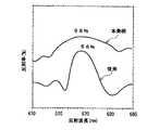
(AlxGa1−x)vIn1−vP系発光ダイオードのための基板としては、各層の材料と格子整合するように、通常はGaAs基板が用いられる。しかし、GaAs基板のバンドギャップは1.42eVと(AlxGa1−x)vIn1−vP系半導体のそれに比べて小さく、それゆえ(AlxGa1−x)vIn1−vP系半導体の発光波長である550nm〜670nmの発光を吸収してしまうため、活性層から発生する光のうち、基板側に放出される光はチップの内部で吸収され、外部にとりだすことができない。したがって、(AlxGa1−x)vIn1−vP系発光ダイオードにおいて、高効率・高輝度の発光ダイオードを作製するためには、図11中に示すように、GaAs基板1と活性層6との間に、屈折率の小さい層と大きい層を順次組み合わせ、多重反射によって反射率を上げた分布帰還形光反射層(Distributed Bragg Reflector (DBR))4を設けることが重要である。この図11の例では、活性層の発光波長570nmを吸収しない(Al0.65Ga0.35)0.51In0.49P(屈折率3.51)を高屈折率材料に、Al0.51In0.49P(屈折率3.35)を低屈折率材料に選び、発光波長λに対し低屈折率材料、高屈折率材料各層の光学的膜厚をλ/4に設定し、これらの材料を交互に10ペア分積層することによって、反射率を向上させ、トータルの光反射層の反射率を約50%にしている。図13(a)は、このようなAlGaInP系光反射層を設けた場合のペア数に対する反射率の特性を示している。図中に「AlInP/Q(0.4)」と記載されているのは、(Al0.65Ga0.35)0.51In0.49PとAl0.51In0.49Pとのペアを用いた場合の特性を意味する。同様に、「AlInP/Q(0.5)」と記載されているのは、(Al0.55Ga0.45)0.51In0.49PとAl0.51In0.49Pとのペアを用いた場合の特性を意味する。この光反射層を採用した場合、光反射層のない場合に比べ、チップ光度を20mcdから35mcdに向上させることができる。
【0009】
なお、良く知られているように、光学的膜厚は、結晶の層厚をd、屈折率をnとしたときndで与えられる。
【0010】
(AlxGa1−x)vIn1−vP系発光ダイオードにおいては、図12に示すように、AlxGa1−xAsとAlAsとのペアを積層してなり、GaAs基板と格子整合する光反射層14が使用される。図13(b)は、このようなAlGaAs系光反射層14を設けた場合のペア数に対する反射率の特性を示している。図中に「Al0.60」と記載された点線は、活性層の発光波長570nmを吸収しないAl0.65Ga0.35As(屈折率3.66)を高屈折率材料に、AlAs(屈折率3.10)を低屈折率材料に選び、これらの材料を交互にペアとして積層してなる光反射層を設けた場合の特性を示している。同様に、図中に「Al0.70」と記載された破線は、Al0.70Ga0.30AsとAlAsとのペアを用いた場合の特性、図中に「Al0.75」と記載された実線は、Al0.65Ga0.35AsとAlAsとのペアを用いた場合の特性を示している。この結果、Al0.65Ga0.35As(屈折率3.66)を高屈折材料に、AlAs(屈折率3.10)を低屈折率材料に選んだ場合には、図13(a)に示した例に比べてより屈折率差を設けることができ、光反射層のトータルの反射率を約60%にすることが可能である。この光反射層を採用した場合、光反射層のない場合に比べ、チップ光度を20mcdから40mcdに向上させることができる。
【0011】
【発明が解決しようとする課題】
ところで、図13(a)(b)から分かるように、光度を2倍以上に改善できる90%以上の高反射率を得るためには、光反射層4,14を構成する半導体層ペアの数を30以上にする必要がある。これは、(AlxGa1−x)0.51In0.49P(x=0.45)/Al0.51In0.49Pの場合は屈折率差が0.18、AlAs/AlxGa1−xAsの場合は屈折率差が0.32程度と、それぞれ屈折率差が非常に小さいためである。
【0012】
しかしながら、ペア数を30以上にすると、成長時間が長くなってしまい、量産性に乏しくなる。また、屈折率差が小さいと、反射スペクトルの半値幅が狭くなってしまい、光反射層の層厚が少し変動するだけで、反射スペクトルが大きくシフトするため、発光波長と光反射層を合わせることが困難になり、再現性ひいては量産性に乏しくなる。また、ペア数が多くなると、光反射層だけで3μm以上の厚膜になってしまい、エピタキシャル成長後の基板が反ったり、変形しやすなり、その後の工程にかけにくくなる。
【0013】
この事情は、AlGaInP系材料に限らず、他の様々な材料を用いた半導体発光素子でも同様である。
【0014】
そこで、この発明の課題は、活性層から放出された光を有効に外部に取り出すことができる半導体発光素子を提供することにある。
【0015】
また、この発明の課題は、そのような半導体発光素子を量産性良く作製できる半導体発光素子の製造方法を提供することにある。
【0016】
また、この発明の課題は、そのような半導体発光素子を備えたLEDランプおよびLED表示装置を提供することにある。
【0017】
【課題を解決するための手段】
上記課題を解決するため、この発明の半導体発光素子は、次のように構成される。すなわち、この発明の半導体発光素子は、
半導体基板上に所定の波長の光を発生する半導体からなる活性層を含む複数の層が積層されてなる半導体発光素子において、
上記半導体基板と活性層との間に、Alを含む半導体層からなる副反射部分と、Alを含む誘電体からなり、上記副反射部分よりも上記活性層からの光に対する反射率が高い主反射部分とを、層方向に連なって有する第1の光反射層を備え、
上記半導体基板は第1導電型であり、
上記活性層の上に第2導電型の電流拡散層が設けられ、
上記電流拡散層の内部の所定領域に設けられた第1導電型の電流阻止層と、
上記電流拡散層の上部表面で上記電流阻止層に対応する領域に設けられた電極層とを備え、
上記第1の光反射層の副反射部分は上記電流阻止層に対応する領域に配置され、
上記第1の光反射層の主反射部分は上記電流阻止層の周りに対応する領域に配置されていることを特徴とする。
【0018】
この発明の半導体発光素子では、上記半導体基板と活性層との間に、Alを含む半導体層からなる副反射部分と、Alを含む誘電体からなり、上記副反射部分よりも上記活性層からの光に対する反射率が高い主反射部分とを、層方向に連なって有する第1の光反射層を備えている。したがって、上記活性層が発した光は第1の光反射層の主反射部分によって高い反射率で反射される。第1の光反射層の主反射部分を必要な領域、例えば活性層上に電極が存在しない領域に配置すれば、上記活性層が発した光は第1の光反射層の主反射部分によって反射され、電極に遮られることなく外部へ出射する。したがって、活性層から放出された光を有効に外部に取り出すことができる。
【0019】
また、この半導体発光素子では、電極層から電流拡散層に注入された通電電流は、上記電流拡散層の内部の所定領域に設けられた電流阻止層によって遮られて、電流阻止層の周りの領域に多く流れる。この結果、活性層のうち上記電流阻止層の周りに相当する部分が多く発光する。上記第1の光反射層の主反射部分は上記電流阻止層の周りに対応する領域に配置されているので、上記活性層のうち上記電流阻止層の周りに相当する部分が発した光は第1の光反射層の主反射部分によって反射され、電極に遮られることなく外部へ出射する。したがって、活性層から放出された光を有効に外部に取り出すことができる。
【0020】
一実施形態の半導体発光素子は、上記第1の光反射層と活性層との間に、上記活性層からの光を反射するように、低屈折率材料層と高屈折率材料層とのペアを複数積層してなる第2の光反射層を備えたことを特徴とする。
【0021】
この一実施形態の半導体発光素子では、上記第1の光反射層と活性層との間に、上記活性層からの光を反射するように、低屈折率材料層と高屈折率材料層とのペアを複数積層してなる第2の光反射層を備えるので、活性層から放出された光をさらに有効に外部に取り出すことができる。また、第1の光反射層の主反射部分はAlを含む誘電体からなるので、Alを含む半導体層からなる副反射部分よりも屈折率nが低くなる。第1の光反射層の主反射部分の屈折率nが低いので、第2の光反射層のペア数が少なくとも反射率が高くなる。
【0022】
なお、第2の光反射層は、分布帰還形光反射層(Distributed Bragg Reflector (DBR))であるのが望ましい。
【0023】
一実施形態の半導体発光素子では、上記第1の光反射層の副反射部分はAlxGa1−xAs、(AlxGa1−x)vIn1−vP、(AlxGa1−x)vIn1−vN、(AlxGa1−x)vIn1−vAs、(AlxGa1−x)vIn1−vSb(ただし、0<x≦1、0<v<1である。)のうちいずれか一種類の半導体からなる。また、上記第1の光反射層の主反射部分はAlOy(ただし、yは正の実数である。)からなる。
【0024】
この明細書では、酸化アルミニウムの表記をAlOyで統一する。AlOyはAlxOy(ただし、xとyは正の実数である。)と同義である。
【0025】
なお、組成を表すx、v、y等は、異なる化合物間では独立の値をとり得るものとする。
【0026】
また、一実施形態の半導体発光素子では、上記第1の光反射層の副反射部分はAlxGa1−xAs層とAlzGa1−zAs層とを交互に積層した多層膜、(AlxGa1−x)vIn1−vP層と(AlzGa1−z)vIn1−vP層とを交互に積層した多層膜、(AlxGa1−x)vIn1−vN層と(AlzGa1−z)vIn1−vN層とを交互に積層した多層膜、(AlxGa1−x)vIn1−vAs層と(AlzGa1−z)vIn1−vAs層とを交互に積層した多層膜、(AlxGa1−x)vIn1−vSb層と(AlzGa1−z)vIn1−vSb層とを交互に積層した多層膜(ただし、0<x<z≦1、0<v<1である。)のうちいずれか一組の多層膜からなる。また、上記第1の光反射層の主反射部分は、上記副反射部分をなす上記多層膜に対応したAlxGa1−xAs、(AlxGa1−x)vIn1−vP、(AlxGa1−x)vIn1−vN、(AlxGa1−x)vIn1−vAs、(AlxGa1−x)vIn1−vSb(ただし、0<x≦1、0<v<1である。)のうちいずれか一種類の半導体とAlOy層(ただし、yは正の実数である。)とを交互に積層したものからなる。
【0027】
さて、従来技術に関して述べたように、光反射層により高反射率を得て光取り出し効率を上げ、高輝度化・高出力化を達成するためには、光反射層が単一の層の場合には光反射層の反射面を挟む2層の屈折率の差を大きくすることが必要である。また、光反射層が多層膜で構成されている場合は光反射層を構成する1対の半導体膜の屈折率差を大きくしなければならない。しかし、例えば(AlxGa1−x)vIn1−vP系の発光ダイオードの場合、光吸収がなくて活性層に格子整合する材料系は、いずれも化合物半導体材料である(AlxGa1−x)vIn1−vP系か、AlxGa1−xAs系に限られており、屈折率を変えることができるのはせいぜい2.9〜3.5程度の範囲内に止まる。
【0028】
一方、本発明の反射層の原理図を図1に示す。半導体基板a上に、AlAsを酸化したAlOy酸化層b、AlxGa1−xAs層と、高屈折率半導体材料と低屈折率半導体材料とを交互に積層してなる光反射層cと、活性層dとをこの順に堆積した構造である。これに対し、従来はAlOy酸化層bがなかった。このようにした場合、光反射層cとAlOy層bとの間に0.6〜1.4程度の大きな屈折率差が設けることができる。したがって、光反射層cとAlOy層bとの界面での反射率が大きくなり、通常の光反射層に比べ大きな反射率が得られる。例えば図2に示すように、本発明によれば、AlOy層を設けない場合(従来)に比して、反射率が高く、しかも、反射スペクトルの半値幅を大きくすることができる(反射率の高い波長範囲が広い)。
【0029】
一方、図3に本発明の別の反射層の原理図を示す。半導体基板a上に、AlAs層とAlxGa1−xAs層を交互に積層し、上記AlAs層をAlOy層(ただし、yは正の実数である。)bに変化させた光反射層fと活性層dとをこの順に堆積した構造である。従来のAlAs層とAlxGa1−xAs層を交互に積層したままの光反射層に比べ、AlOy層とAlxGa1−xAs層との間の屈折率差は0.6〜1.4程度と大きくできる。この結果、光反射層fの反射特性は図4に示すように反射率の最大値は99%と高くなり、その波長範囲も広くなる。更に、必要な波長範囲から外れた波長の光に対しては反射率が急に小さくなるために半導体発光素子の色純度が高くなるという利点もある。図1の場合と同様に、層厚のバラツキや変動があったとしても、反射率や反射スペクトルは変動しにくく、量産性に優れる。
【0030】
Alは酸素との結合が強いために極めて酸化されやすい性質があり、大気中に放置するだけでAl酸化物が形成される。ただ、このように自然に酸化しただけのAl酸化膜は膜に穴が多い等特性が良くない。したがって、例えばAlxGa1−xAs層(特にAl混晶比xが1に近いもの)を300℃〜400℃の温度で水蒸気雰囲気中に放置すると高温の水蒸気により酸化されて、より安定なAlOy層を形成することができる(例えば、米国特許5,517,039号明細書、または、伊賀健一他著「面発光レーザの基礎と応用」、共立出版株式会社、1999年6月、p.105−113)。このAlOy層は、酸化物(誘電体)であるため、屈折率nが半導体材料に比べて極めて低く、n=2.5〜1.9の値をとる。したがって、上記AlxGa1−xAs層をAlOy層に変化させて屈折率を低くすることによって、上記活性層が発した光に対する反射率を高めることができる。したがって、光反射層のペア数が少なくても反射率が高く、活性層から放出された光を有効に外部に取り出すことができる。
【0031】
また、AlOy層は、酸化物(誘電体)であるからバンドギャップが大きく、青色から赤色の可視光領域に対し透明である。したがって、本発明によれば、波長依存性が極めて小さく、かつ反射率が100%に近い良質の光反射層の形成が可能である。したがって、従来の半導体材料による光反射層のように、発光波長に対して吸収がないAl組成をわざわざ選ぶ必要がない。
【0032】
本発明によれば、AlOy層を設けない場合(従来)に比して、反射率が高く、しかも、反射スペクトルの半値幅を大きくすることができる。この結果、光反射層の層厚のバラツキや変動があったとしても、反射率や反射スペクトルは変動しにくい。したがって、量産性に優れる。
【0033】
光反射層を構成する低屈折率のAlリッチ層f2がさらに低屈折率のAlOy層になるので、上記活性層が発した光に対する反射率を高めることができる。したがって、光反射層のペア数が少なくても反射率が高く、活性層から放出された光を有効に外部に取り出すことができる。例えば図4に示すように、本発明によれば、AlOy層に変化させない場合(従来)に比して、反射率が高く、しかも、反射スペクトルの半値幅を大きくすることができる。この結果、光反射層の層厚のバラツキや変動があったとしても、反射率や反射スペクトルは変動しにくい。したがって、量産性に優れる。
【0034】
図5は、本発明による光反射層の反射率のペア数依存性を、従来例と比較して示している。図中、●印を結ぶ実線αは、本発明に基づいて低屈折率のAlOy層と高屈折率のAl0.60Ga0.40As層とのペアを用いた場合の特性を示している。その他の線β1,β2,β3,β4,β5は公知のペアを用いた場合の特性を示している。具体的には、β1はAl0.75Ga0.25As層とAlAs層とのペア、β2はAl0.70Ga0.30As層とAlAs層とのペア、β3はAl0.60Ga0.40As層とAlAs層とのペア、β4は(Al0.40Ga0.60)0.51In0.49P層とAl0.51In0.49P層とのペア、β5(Al0.50Ga0.50)0.51In0.49P層とAl0.51In0.49P層とのペアを用いた場合の特性をそれぞれ示している。図から分かるように、本発明によれば光反射層は屈折率差が大きいために、数ペアの光反射層でもほぼ100%に近い反射率が得られる。したがって、成長時間を短くでき、量産性も高い。
【0035】
この発明の半導体発光素子の製造方法は、次のように構成される。すなわち、この発明の半導体発光素子の製造方法は、上記発明の半導体発光素子を作製する半導体発光素子の製造方法である。そして、
上記半導体基板と活性層との間に、上記複数の層のうちの他の層よりもAlの割合が多いAlリッチ層を設ける工程と、
上記複数の層を積層したウェハをチップ単位に分割し、上記Alリッチ層の側面を露出させる工程と、
上記露出した側面から上記Alリッチ層に含まれたAlを酸化させて、そのAlリッチ層の周辺部分をAlOy層に変化させて、得られたAlOy層を上記主反射部分とする一方、上記Alリッチ層のうちの残りの部分を上記副反射部分とする工程と、
を有する。
【0036】
この発明の半導体発光素子の製造方法によれば、上記Alリッチ層の周辺部分をAlOy層(誘電体)に変化させて屈折率を低くすることによって、上記活性層が発した光に対する反射率を高めることができる。したがって、活性層から放出された光を有効に外部に取り出すことができる。
【0037】
一実施形態の半導体発光素子の製造方法では、上記Alリッチ層に含まれたAlを酸化させる工程を、上記Alリッチ層の側面が露出したチップを水蒸気中に放置して行うことを特徴とする。
【0038】
一実施形態の半導体発光素子の製造方法では、上記水蒸気を、沸騰水中を通した不活性ガス(Ar、窒素等)により上記Alリッチ層の側面に導入することを特徴とする。
【0039】
一実施形態の半導体発光素子の製造方法では、上記Alリッチ層に含まれたAlを酸化させる工程を、300℃乃至400℃の温度の雰囲気中で行うことを特徴とする。
【0040】
なお、上記Alリッチ層の周辺部分に生じた上記AlOy層をエッチングにより除去する工程を有しても良い。
【0041】
そのようにした場合、AlOy層が除去されて生じた空間領域の屈折率は1であるから、活性層の裏側のチップ周辺領域で全反射に近い状態が得られる。したがって、活性層から放出された光を有効に外部に取り出すことができる。
【0042】
また、この発明のLEDランプは、この発明の半導体発光素子を備えたことを特徴とする。
【0043】
一実施形態のLEDランプは、上記半導体発光素子として互いに波長が異なる複数の半導体発光素子を一体に備え、これらの半導体発光素子が独立に通電されるように接続されていることを特徴とする。
【0044】
また、この発明のLED表示装置は、そのようなLEDランプがマトリックス状に配置されていることを特徴とする。
【0045】
一実施形態の半導体発光素子の製造方法では、上記Alリッチ層のうち上記AlOy層に変化されない残りの部分に対応する上記活性層上の領域に、通電用の電極を形成することを特徴とする。
【0046】
この一実施形態の半導体発光素子の製造方法では、上記Alリッチ層のうち上記AlOy層に変化されない残りの部分に対応する上記活性層上の領域に、電極が形成される。したがって、上記Alリッチ層のうち上記AlOy層に変化された部分に対応する領域を、電極が占めるのを避けることができる。したがって、上記活性層で発生し上記AlOy層で反射された光が、上記電極に遮られることなく、有効に外部に取り出される。
【0047】
一実施形態の半導体発光素子の製造方法では、上記Alリッチ層のうち上記AlOy層に変化されない残りの部分に対応する領域に、通電電流を妨げる電流阻止層を形成することを特徴とする。
【0048】
この一実施形態の半導体発光素子の製造方法では、上記Alリッチ層のうち上記AlOy層に変化されない残りの部分に対応する領域に、通電電流を妨げる電流阻止層が形成される。したがって、上記電流阻止層が形成されない場合に比して、上記AlOy層に対応する領域に通電電流が多く流れる。したがって、上記活性層で発生し上記AlOy層で反射された光が、有効に外部に取り出される。
【0049】
一実施形態の半導体発光素子の製造方法では、上記光反射層は所定のAl混晶比を持つAlを含む層とAlOy層との交互の積層からなり、上記AlOy層に変化されたAlを含む層に隣接する、上記光反射層をなす層の1層の厚さを、上記波長の4分の1に設定することを特徴とする。
【0050】
一実施形態の半導体発光素子の製造方法では、上記各層をチップ単位に分割した後、上記Alリッチ層を露出した端面から上記AlOy層に変化させて、上記Alリッチ層のうち上記AlOy層に変化されない残りの部分の形状と上記活性層上の上記電極の形状とを一致させることを特徴とする。
【0051】
この一実施形態の半導体発光素子の製造方法によれば、従来の半導体材料による光反射層のように、発光波長に対して吸収がないAl組成をわざわざ選ぶ必要がない。
【0052】
また、別の面から、この発明の半導体発光素子は、半導体基板上に所定の波長を持つ光を発生する発光層を有する半導体発光素子において、上記半導体基板と発光層との間に、上記発光層が発した光を反射するように、層方向に関して屈折率が変化している半導体層が設けられていることを特徴とする。
【0053】
ここで「層方向」とは、層に沿った方向、つまり層が広がっている方向(面方向)を意味する。
【0054】
この発明の半導体発光素子では、上記半導体基板と発光層との間に、上記発光層が発した光を反射するように、層方向に関して屈折率が変化している半導体層が設けられている。この半導体層の屈折率を必要な領域、例えば発光層上に電極が存在しない領域で屈折率を低くすることによって、上記発光層が発した光に対する反射率を高めることができる。したがって、光反射層のペア数が少なくても反射率が高く、発光層から放出された光を有効に外部に取り出すことができる。
【0055】
さて、既に述べたように、光反射層により高反射率を得て光取り出し効率を上げ、高輝度化・高出力化を達成するためには、光反射層を構成する1対の半導体膜の屈折率差を大きくしなければならない。しかし、例えば(AlxGa1−x)vIn1−vP系の発光ダイオードの場合、光吸収がなくて発光層に格子整合する材料系は、いずれも化合物半導体材料である(AlxGa1−x)vIn1−vP系か、AlxGa1−xAs系に限られており、屈折率を変えることができるのはせいぜい2.9〜3.5程度の範囲内に止まる。
【0056】
そこで、本発明の半導体発光素子の製造方法では、半導体基板上に所定の波長を持つ光を発生する発光層を設ける半導体発光素子の製造方法において、上記半導体基板上にAlxGa1−xAs層と、上記発光層とをこの順に堆積し、層方向に関して上記AlxGa1−xAs層の一部をAlOy層(ただし、yは正の実数である。)に変化させることを特徴とする。
【0057】
AlxGa1−xAs層中のAlは酸素との結合が強いために極めて酸化されやすい性質があり、大気中に放置するとAl酸化物が形成される。したがって、AlxGa1−xAs層(特にAl混晶比xが1に近いもの)を300℃〜400℃の温度で水蒸気中で酸化すると、安定なAlOy層が形成される。このAlOy層は、Alを含む酸化物であるため、屈折率nが半導体材料に比べて極めて低く、n=2.5〜1.9の値をとる。したがって、上記AlxGa1−xAs層をAlOy層に変化させて屈折率を低くすることによって、上記発光層が発した光に対する反射率を高めることができる。したがって、光反射層のペア数が少なくても反射率が高く、発光層から放出された光を有効に外部に取り出すことができる。
【0058】
また、AlOy層は、酸化物であるからバンドギャップが大きく、可視光領域、特に(AlxGa1−x)vIn1−vP系の発光領域である560nm〜650nmに対し透明である。したがって、本発明によれば、波長依存性が極めて小さく、かつ反射率が100%に近い良質の光反射層の形成が可能である。したがって、従来の半導体材料による光反射層のように、発光波長に対して吸収がないAl組成をわざわざ選ぶ必要がない。
【0059】
一実施形態の半導体発光素子の製造方法では、図1に例示するように、半導体基板a上に、AlxGa1−xAs層と、高屈折率半導体材料と低屈折率半導体材料とを交互に積層してなる光反射層cと、発光層dとをこの順に堆積し、層方向に関して上記AlxGa1−xAs層の一部をAlOy層bに変化させる(ただし、図1ではAlOy層に変化した領域のみを示している。)。このようにした場合、光反射層cとAlOy層bとの間に0.6〜1.4程度の大きな屈折率差が設けることができる。したがって、光反射層cとAlOy層bとの界面での反射率が大きくなり、通常の光反射層に比べ大きな反射率が得られる。例えば図2に示すように、本発明によれば、AlOy層を設けない場合(従来)に比して、反射率が高く、しかも、反射スペクトルの半値幅を大きくすることができる。この結果、光反射層の層厚のバラツキや変動があったとしても、反射率や反射スペクトルは変動しにくい。したがって、量産性に優れる。
【0060】
一実施形態の半導体発光素子の製造方法では、図3に例示するように、半導体基板a上に、高屈折率の半導体材料f1と低屈折率のAlxGa1−xAs層f2(ただし、0<x≦1である。)との交互の積層からなる光反射層fと、発光層dとをこの順に堆積し、層方向に関して上記AlxGa1−xAs層f2の一部をAlOy層に変化させる(ただし、図3ではAlOy層に変化した領域(点描)のみを示している。)。このようにした場合、光反射層を構成する低屈折率のAlxGa1−xAs層f2層がさらに低屈折率のAlOy層になるので、上記発光層が発した光に対する反射率を高めることができる。したがって、光反射層のペア数が少なくても反射率が高く、発光層から放出された光を有効に外部に取り出すことができる。例えば図4に示すように、本発明によれば、AlOy層に変化させない場合(従来)に比して、反射率が高く、しかも、反射スペクトルの半値幅を大きくすることができる。この結果、光反射層の層厚のバラツキや変動があったとしても、反射率や反射スペクトルは変動しにくい。したがって、量産性に優れる。
【0061】
図5は、本発明による光反射層の反射率のペア数依存性を、従来例と比較して示している。本発明によれば光反射層は屈折率差が大きいために、数ペアの光反射層でもほぼ100%に近い反射率が得られる。したがって、成長時間を短くでき、量産性も高い。
【0062】
一実施形態の半導体発光素子の製造方法では、層方向に関して上記AlxGa1−xAs層の一部をAlOy層に変化させた後、そのAlOy層を除去することを特徴とする。
【0063】
この一実施形態の半導体発光素子の製造方法では、AlOy層が除去されて生じた空間領域の屈折率は1であるから、発光層の裏側のチップ周辺領域で全反射に近い状態が得られる。したがって、発光層から放出された光を有効に外部に取り出すことができる。
【0064】
一実施形態の半導体発光素子の製造方法では、上記AlxGa1−xAs層のうち上記AlOy層に変化されない残りの部分に対応する上記発光層上の領域に、通電用の電極を形成することを特徴とする。
【0065】
この一実施形態の半導体発光素子の製造方法では、上記AlxGa1−xAs層のうち上記AlOy層に変化されない残りの部分に対応する上記発光層上の領域に、電極が形成される。したがって、上記AlxGa1−xAs層のうち上記AlOy層に変化された部分に対応する領域を、電極が占めるのを避けることができる。したがって、上記発光層で発生し上記AlOy層で反射された光が、上記電極に遮られることなく、有効に外部に取り出される。
【0066】
一実施形態の半導体発光素子の製造方法では、上記AlxGa1−xAs層のうち上記AlOy層に変化されない残りの部分に対応する領域に、通電電流を妨げる電流阻止層を形成することを特徴とする。
【0067】
この一実施形態の半導体発光素子の製造方法では、上記AlxGa1−xAs層のうち上記AlOy層に変化されない残りの部分に対応する領域に、通電電流を妨げる電流阻止層が形成される。したがって、上記電流阻止層が形成されない場合に比して、上記AlOy層に対応する領域に通電電流が多く流れる。したがって、上記発光層で発生し上記AlOy層で反射された光が、有効に外部に取り出される。
【0068】
一実施形態の半導体発光素子の製造方法では、上記光反射層は所定のAl混晶比を持つAlxGa1−xAs層(ただし、0<x≦1である。)とAlOy層との交互の積層からなり、上記AlOy層に変化されたAlxGa1−xAs層に隣接する、上記光反射層をなすAlxGa1−xAs層の1層の厚さを、上記波長の4分の1に設定することを特徴とする。
【0069】
この一実施形態の半導体発光素子の製造方法によれば、上記AlOy層に対応する領域で、上記発光層が発した光に対する反射率がさらに高まる。
【0070】
一実施形態の半導体発光素子の製造方法では、上記発光層を(AlxGa1−x)vIn1−vP系材料で形成することを特徴とする半導体発光素子の製造方法。
【0071】
この一実施形態の半導体発光素子の製造方法によれば、発光波長帯560nm〜650nmの半導体発光素子が作製される。
【0072】
一実施形態の半導体発光素子の製造方法では、上記各層をチップ単位に分割した後、上記AlxGa1−xAs層を露出した端面から上記AlOy層に変化させて、上記AlxGa1−xAs層のうち上記AlOy層に変化されない残りの部分の形状と上記発光層上の上記電極の形状とを一致させることを特徴とする。
【0073】
この一実施形態の半導体発光素子の製造方法では、上記AlxGa1−xAs層を露出した端面から上記AlOy層に変化させるので、AlOy層を安定かつ容易に形成できる。したがって、量産性に優れる。しかも、上記AlxGa1−xAs層のうち上記AlOy層に変化されない残りの部分の形状と上記発光層上の上記電極の形状とを一致させるので、上記AlxGa1−xAs層のうち上記AlOy層に変化された部分に対応する領域を、電極が占めるのを避けることができる。したがって、上記発光層で発生し上記AlOy層で反射された光が、上記電極に遮られることなく、有効に外部に取り出される。
【0074】
一実施形態の半導体発光素子の製造方法では、上記各層をチップ単位に分割した後、上記AlxGa1−xAs層を露出した端面から上記AlOy層に変化させて、上記AlxGa1−xAs層のうち上記AlOy層に変化されない残りの部分の形状と上記電流阻止層の形状とを一致させることを特徴とする。
【0075】
この一実施形態の半導体発光素子の製造方法では、上記AlxGa1−xAs層を露出した端面から上記AlOy層に変化させるので、AlOy層を安定かつ容易に形成できる。したがって、量産性に優れる。しかも、上記AlxGa1−xAs層のうち上記AlOy層に変化されない残りの部分の形状と上記電流阻止層の形状とを一致させるので、上記AlOy層に対応する領域に通電電流が多く流れる。したがって、上記発光層で発生し上記AlOy層で反射された光が、有効に外部に取り出される。
【0076】
一実施形態の半導体発光素子の製造方法では、上記AlxGa1−xAs層に代えて、AlxGa1−xP層、AlxIn1−xP層またはAlxIn1−xAs層を用いることを特徴とする。
【0077】
また、本発明の半導体発光素子の製造方法は、半導体基板上に所定の波長を持つ光を発生する発光層を設ける半導体発光素子の製造方法において、上記半導体基板上に、所定のAl混晶比を持つAlxGa1−xAs層(ただし、0<x≦1である。)と(AlxGa1−x)vIn1−vP層(ただし、0<x≦1、0<v<1である。)との交互の積層からなり上記波長の光を反射するための光反射層と、上記発光層とをこの順に堆積し、層方向に関して上記AlxGa1−xAs層の一部をAlOy層(ただし、yは正の実数である。)に変化させることを特徴とする。
【0078】
この発明の半導体発光素子の製造方法によれば、上記AlxGa1−xAs層をAlOy層に変化させて屈折率を低くすることによって、上記発光層が発した光に対する反射率を高めることができる。したがって、光反射層のペア数が少なくても反射率が高く、発光層から放出された光を有効に外部に取り出すことができる。
【0079】
また、AlOy層は、酸化物であるからバンドギャップが大きく、可視光領域、特に(AlxGa1−x)vIn1−vP系の発光領域である560nm〜670nmに対し透明である。したがって、本発明によれば、波長依存性が極めて小さく、かつ反射率が100%に近い良質の光反射層の形成が可能である。したがって、従来の半導体材料による光反射層のように、発光波長に対して吸収がないAl組成をわざわざ選ぶ必要がない。
【0080】
一実施形態の半導体発光素子の製造方法は、層方向に関して上記AlxGa1−xAs層の一部をAlOy層に変化させた後、そのAlOy層を除去するとき、ふっ酸系のエッチング液を用いることを特徴とする。
【0081】
この一実施形態の半導体発光素子の製造方法によれば、上記AlOy層のみをAlxGa1−xAs層等に対して選択的にエッチングして除去することができる。
【0082】
【発明の実施の形態】
以下、この発明を図示の実施の形態により詳細に説明する。
【0083】
(第1実施形態)
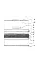
図6は第1実施形態の半導体発光ダイオードの断面構造を示している。この実施形態は、第1の光反射層の主反射部分がAlOy単層(ただし、yは正の実数である。)からなる点に特徴がある。
【0084】
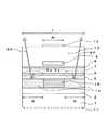
この発光ダイオードは、n型GaAs基板1の上に、n型GaAsバッファ層(例えば厚さ0.5μm、不純物濃度5×1017cm−3)2と、第1の光反射層として層方向に連なるように設けられた副反射部分としてのn型AlAs電導層3および主反射部分としてのAlOy酸化層13とを備えている。副反射部分としてのn型AlAs電導層3はチップの中央領域に配置され、主反射部分としてのAlOy酸化層13はその周りを取り巻くようにチップの周辺領域に配置されている。この発光ダイオードは、その上に、(AlxGa1−x)0.51In0.49P下部クラッド層(0≦x≦1、例えばx=1.0、厚さ1.0μm、不純物濃度5×1017cm−3)5と、p型(AlxGa1−x)vIn1−vP活性層(0≦x≦1、例えばx=0.42、厚さ0.6μm、不純物濃度1×1017cm−3)6と、p型(AlxGa1−x)0.51In0.49P上部クラッド層(0≦x≦1、例えばx=1.0、厚さ1.0μm、不純物濃度5×1017cm−3)7と、p型(AlxGa1−x)vIn1−vP中間層(x=0.2、v=0.4、厚さ0.15μm、不純物濃度1×1018cm−3)8とをこの順に備えている。この発光ダイオードは、さらにその上にp型(AlxGa1−x)vIn1−vP電流拡散層(x=0.05、v=0.05、トータル厚さ8.5μm、不純物濃度5×1018cm−3)10を備え、この電流拡散層中の中央領域に形成された、通電電流を妨げるためのn型GaP電流阻止層(厚さ0.3μm、不純物濃度1×1018cm−3)9を備えている。11はn側電極、12はp側電極である。
【0085】
この発光ダイオードは次のようにして作製される。
【0086】
i) n型GaAs基板1上の全域に、n型GaAsバッファ層(例えば厚さ0.5μm、不純物濃度5×1017cm−3)2と、Alリッチ層としてのn型AlAs電導層3と、(AlxGa1−x)0.51In0.49P下部クラッド層(0≦x≦1、例えばx=1.0、厚さ1.0μm、不純物濃度5×1017cm−3)5と、活性層としてのp型(AlxGa1−x)vIn1−vP活性層(0≦x≦1、例えばx=0.42、厚さ0.6μm、不純物濃度1×1017cm−3)6と、p型(AlxGa1−x)0.51In0.49P上部クラッド層(0≦x≦1、例えばx=1.0、厚さ1.0μm、不純物濃度5×1017cm−3)7と、p型(AlxGa1−x)vIn1−vP中間層(x=0.2、v=0.4、厚さ0.15μm、不純物濃度1×1018cm−3)8とをこの順に堆積する。
【0087】
ii) 次に、p型(AlxGa1−x)vIn1−vP中間層8上にp型(AlxGa1−x)vIn1−vP電流拡散層(x=0.05、v=0.05、厚さ1.5μm、不純物濃度5×1018cm−3)10を成長し、その上にn型GaP電流阻止層(厚さ0.3μm、不純物濃度1×1018cm−3)9を成長する。その後、n型GaP電流阻止層9をフォトリソグラフィによる選択エッチングによってM=100μm角〜150μm角にパターン加工して、その周囲に通電電流のための電流経路を作る。その後、p型(AlxGa1−x)vIn1−vP電流拡散層(x=0.05、v=0.05、厚さ7μm、不純物濃度5×1018cm−3)10を再成長する。
【0088】
iii) 次に、p側に電極となる金属層を設け、フォトリソグラフィによる選択エッチングによって電流阻止層9の位置に合わせて電極12をM=100μm角〜150μm角にパターン加工する。その後、基板1の裏面側から厚さ120μm程度に薄く研磨し、n側にも電極11を形成する(この状態の基板をウェハと呼ぶ。通常、直径50mm程度の大きさのものである。)。通常のブレーキング方法と同様に、このウェハの裏面側を粘着シートに貼り付けた後、ダイシングソーを用いて電極12のパターンに沿ってウェハの厚さの途中まで溝を切り、その後、粘着シートを引張って広げる。これにより、ウェハをL=280μm角の大きさのチップに分割する。
【0089】
iv) チップに分割することによりチップ側面にAlAs層3が露出する。この状態で各チップを温度400℃、窒素雰囲気中の酸化膜形成装置(図示せず)に入れる。酸化膜形成装置内部に沸騰水中を通した窒素ガスを流し込むことにより、この酸化膜形成装置内を高温の水蒸気で満たす。この高温の水蒸気が上記AlAs層3の露出した側面に導入されると、チップ側面端部から内部へ一定の速度で酸化が進行し、元のAlAs層3のうち周辺部分をAlOy層13に変化させることができる(例えば、米国特許5,517,039号明細書、または、伊賀健一他著「面発光レーザの基礎と応用」、共立出版株式会社、1999年6月、p.105−113))。このAlOy層13の層方向寸法(酸化の深さ)Nは、この酸化の温度と時間および材料によって決まる。
【0090】
また、単に酸素で酸化させた場合より水蒸気により酸化させた方が良質の酸化膜が得られる、という特徴がある。特に、窒素ガスにより水蒸気を恒温層に持ち込むのは酸素を入れないようにするためである。
【0091】
この層方向寸法NはチップサイズをL、電流阻止層又は電極の1辺の長さをMとして、
N≦(L−M)/2
が望ましい。本実施形態では、AlOy層13の層方向寸法Nが80μmになるように、400℃で3時間、酸化膜形成装置に入れておく。元のAlAs層3の屈折率は3.1であるが、酸化で得られたAlOy層13の屈折率は1.9と低い値になる。従来例では基板での反射率は30%程度であるが、本実施形態では、チップ周辺領域で光反射層の反射率を80%以上に改善できた。
【0092】
また、このように露出したAlAs層3をチップ側面の端部から酸化して、元のAlAs層3のうち周辺部分をAlOy層13に変化させた場合、AlOy層を安定かつ容易に形成でき、量産性に優れる。しかも、AlAs層3のうちAlOy層に変化されない残りの部分の形状と電流阻止層9の形状とを一致させるので、AlOy層13に対応するチップ周辺領域に通電電流が多く流れる。したがって、活性層6の周辺部分6aで光が多く発生する。活性層6の周辺部分6aで発生した光は、チップ周辺領域で光反射層の反射率が改善されているので効率良く反射される。具体的には、活性層6から裏面(基板)側へ放射される光90のうち80%以上をAlOy層13によって表面側へ反射することができる。そして、表面側へ反射された光は、電極12に遮られることなく、有効に外部に取り出される。実際に、本実施形態では、発光波長570nmにおけるチップ光度を、通常の35mcdから50mcdに向上させることができた。このように、輝度が向上して、歩留も改善された。
【0093】
(比較例)
図10は、比較例として、電流阻止層9が省略された構造をもつ半導体発光ダイオードを示している。この半導体発光ダイオードは、p型GaP電流阻止層9が省略されている点以外は、第1実施形態の半導体発光ダイオードと全く同じ、つまり各層の厚さや組成、導電型について全く同じに構成されている。
【0094】
しかし、この比較例の半導体発光ダイオードでは、輝度向上の効果が得られなかった。この理由は次のように考えられる。すなわち、この比較例の半導体発光ダイオードでは、電極12の直下に電流阻止層が存在せず、かつAlOy層13が絶縁層であるために、発光領域が活性層6の中央部分(電極12の直下に相当する部分)6bに限られてしまう。この場合、活性層6の中央部分6bから裏面(基板)側へ放射される光のうち、ごく一部90Bはチップ周辺領域へ進んでAlOy層13によって表面側へ反射されるが、大部分90Cは直下の電導層3に入射し、表面側へ反射されないで基板に吸収されるか、たとえ表面側へ反射されてもp型電極12で遮られて、外部へは取り出されない。その結果、発光効率が改善されず、輝度向上の効果が得られない。実際に、本比較例では、発光波長570nmにおけるチップ光度は、従来構造の35mcdに比べ、逆に10mcdに低下した。
【0095】
(第2実施形態)
図7は第2実施形態の半導体発光ダイオードの断面構造を示している。この実施形態は、第1の光反射層の主反射部分が、AlOy層とAlGaAs層とを交互にペアとして複数積層した多層膜からなる点に特徴がある。
【0096】
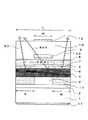
この発光ダイオードは、n型GaAs基板1の上に、n型GaAsバッファ層(例えば厚さ0.5μm、不純物濃度5×1017cm−3)2と、第1の光反射層として層方向に連なるように設けられた副反射部分としてのn型AlAs/AlxGa1−xAs電導型光反射層(例えばx=0.65、不純物濃度5×1017cm−3)15および主反射部分としてのAlOy/AlxGa1−xAs酸化光反射層14とを備えている。副反射部分としてのn型AlAs/AlxGa1−xAs電導型光反射層15はチップの中央領域に配置され、主反射部分としてのAlOy/AlxGa1−xAs酸化光反射層14はその周りを取り巻くようにチップの周辺領域に配置されている。この発光ダイオードは、その上に、(AlxGa1−x)0.51In0.49P下部クラッド層(0≦x≦1、例えばx=1.0、厚さ1.5μm、不純物濃度5×1017cm−3)5と、p型(AlxGa1−x)vIn1−vP活性層(例えばx=0.42、厚さ0.6μm、不純物濃度1×1017cm−3)6と、p型(AlxGa1−x)0.51In0.49P上部クラッド層(0≦x≦1、例えばx=1.0、厚さ1.0μm、不純物濃度5×1017cm−3)7と、p型(AlxGa1−x)vIn1−vP中間層(x=0.2、v=0.4、厚さ0.15μm、不純物濃度1×1018cm−3)8とをこの順に備えている。この発光ダイオードは、さらにその上にp型(AlxGa1−x)vIn1−vP電流拡散層(x=0.05、v=0.05、トータル厚さ8.5μm、不純物濃度5×1018cm−3)10を備え、この電流拡散層中の中央領域に形成された、通電電流を妨げるためのn型GaP電流阻止層(厚さ0.3μm、不純物濃度1×1018cm−3)9を備えている。11はn側電極、12はp側電極である。
【0097】
この発光ダイオードは次のようにして作製される。
【0098】
i) n型GaAs基板1上の全域に、n型GaAsバッファ層(例えば厚さ0.5μm、不純物濃度5×1017cm−3)2と、n型AlAs/AlxGa1−xAs電導型光反射層(例えばx=0.65、不純物濃度5×1017cm−3)15と、(AlxGa1−x)0.51In0.49P下部クラッド層(0≦x≦1、例えばx=1.0、厚さ1.5μm、不純物濃度5×1017cm−3)5と、p型(AlxGa1−x)vIn1−vP活性層(例えばx=0.42、厚さ0.6μm、不純物濃度1×1017cm−3)6と、p型(AlxGa1−x)0.51In0.49P上部クラッド層(0≦x≦1、例えばx=1.0、厚さ1.0μm、不純物濃度5×1017cm−3)7と、p型(AlxGa1−x)vIn1−vP中間層(x=0.2、v=0.4、厚さ0.15μm、不純物濃度1×1018cm−3)8とをこの順に堆積する。
【0099】
ここでn型AlAs/AlxGa1−xAs電導型光反射層15は、Alリッチ層としてのAlAs層と、AlxGa1−xAs層とを交互に積層して構成されている。
【0100】
ii) 次に、p型(AlxGa1−x)vIn1−vP中間層8上にp型(AlxGa1−x)vIn1−vP電流拡散層(x=0.05、v=0.05、厚さ1.5μm、不純物濃度5×1018cm−3)10を成長し、その上にn型GaP電流阻止層(厚さ0.3μm、不純物濃度1×1018cm−3)9を成長する。その後、n型GaP電流阻止層9をフォトリソグラフィによる選択エッチングによってM=100μm角〜150μm角にパターン加工して、その周囲に通電電流のための電流経路を作る。その後、p型(AlxGa1−x)vIn1−vP電流拡散層(x=0.05、v=0.05、厚さ7μm、不純物濃度5×1018cm−3)10を再成長する。
【0101】
iii) 次に、p側に電極となる金属層を設け、フォトリソグラフィによる選択エッチングによって電流阻止層9の位置に合わせて電極12をM=100μm角〜150μm角にパターン加工する。その後、基板1の裏面側から厚さ120μm程度に薄く研磨し、n側にも電極11を形成する。その後、第1実施形態の場合と同様にして、ウェハをL=280μm角の大きさのチップに分割する。
【0102】
iv) この後、チップ側面を大気に露出させてから、第1実施形態の場合と同様にしてn型AlAs/AlxGa1−xAs電導型光反射層15を構成する各AlAs層を側面端部から酸化して、元のAlAs層のうち周辺部分をそれぞれAlOy層に変化させる。すなわち、元のn型AlAs/AlxGa1−xAs電導型光反射層15のうち周辺部分を、低屈折材料層としてのAlOy層と高屈折材料層としてのAlxGa1−xAs層とが交互に複数積層された構造をもつAlOy/AlxGa1−xAs酸化光反射層14に変化させる。このAlOy/AlxGa1−xAs酸化光反射層14の層方向寸法(酸化の深さ)Nは、この酸化の温度と時間によって決まる。この層方向寸法Nは、第1実施形態と同様に、チップの一辺の長さをL、電流阻止層又は電極の1辺の長さをMとして、
N≦(L−M)/2
が望ましい。本実施形態では、第1実施形態の場合と同様に、AlOy/AlxGa1−xAs酸化光反射層14の層方向寸法Nが80μmになるように、400℃で3時間、酸化膜形成装置に入れておく。得られたAlOy/AlxGa1−xAs酸化光反射層14については、低屈折率材料層としてのAlOy層の屈折率が1.9と低くなる(元のAlAs層の屈折率は3.1である。)一方、高屈折率材料層としてのAlxGa1−xAs層の屈折率が3.4のままで変わらない。この理由は、高屈折率材料層としてのAlxGa1−xAs層は、Al混晶比が0.6というようにAlAsに比べ低いため、上述の条件ではチップの側面端部近傍しか酸化膜に変質しないからである。
【0103】
このように、得られたAlOy/AlxGa1−xAs酸化光反射層14は、低屈折率材料層と高屈折率材料層との屈折率差が1.5と大きい分布帰還形光反射層を構成する。通常は低屈折率材料層と高屈折率材料層とが10ペアで光反射層の反射率が55%程度になるが、本実施形態では、わずか5ペアで光反射層の反射率が99%になった。
【0104】
また、このようにn型AlAs/AlxGa1−xAs電導型光反射層15を構成する各AlAs層を側面端部から酸化した場合、分布帰還形光反射層14をチップ周辺領域に安定かつ容易に形成でき、量産性に優れる。しかも、元のn型AlAs/AlxGa1−xAs電導型光反射層15のうちAlOy層に変化されない残りの部分の形状と電流阻止層9の形状とを一致させるので、AlOy/AlxGa1−xAs酸化光反射層14に対応するチップ周辺領域に通電電流が多く流れる。したがって、活性層6の周辺部分6aで光が多く発生する。活性層6の周辺部分6aで発生した光90は、チップ周辺領域で光反射層の反射率が改善されているので効率良く反射され、電極12に遮られることなく、有効に外部に取り出される。実際に、本実施形態では、発光波長570nmにおけるチップ光度を、通常の35mcdから60mcdに向上させることができた。また、反射スペクトルの半値幅が通常の光反射層の半値幅約20nmに比べ5倍以上大きくなった。そのため、量産時に光反射層15の層厚の変動があった場合でも、反射率や反射スペクトルの変動が少なくなり、光度の均一性が向上し、歩留も改善された。
【0105】
(第3実施形態)
第3実施形態の発光ダイオードは、図示を省略するが、図7に示した第2実施形態の半導体発光素子における第1の光反射層の材料を変更した点に特徴がある。
【0106】
この実施形態の発光ダイオードは、第1の光反射層として層方向に連なるように設けられた副反射部分としてのn型AlInP/(AlxGa1−x)vIn1−vP電導型光反射層および主反射部分としてのn型AlOy/(AlxGa1−x)vIn1−vP酸化光反射層を備えている。その他の要素は第2実施形態の半導体発光素子と同じである。
【0107】
ここで、副反射部分としてのn型AlInP/(AlxGa1−x)vIn1−vP電導型光反射層は、分布帰還形光反射層として、AlInP層と(AlxGa1−x)vIn1−vP層とのペアを複数積層して構成されている。各ペアを構成するAlInP層、(AlxGa1−x)vIn1−vP層の厚さは、発光波長λの4分の1になるように、それぞれ設定されている。
【0108】
本実施形態の発光ダイオードは、第2実施形態の発光ダイオードを作製するのと同じ手順で作製される。特に、第1の光反射層の主反射部分に含まれた各n型AlOy層は、副反射部分に含まれた各AlInP層を、第1実施形態と同様に、酸化膜形成装置に入れてチップ端面側部から酸化して形成したものである。元のAlInP層3の屈折率は3.1であるが、酸化で得られたAlOy層13の屈折率は1.9と低い値になる。従来例では光反射層の反射率50%程度であるが、本実施形態では、チップ周辺領域で光反射層の反射率を99%以上に改善できた。
【0109】
本実施形態のように、酸化される材料がAlInPである場合、酸化される材料がAlAs層である場合に比べて酸化の進行が遅くなる。しかし、ペアをなす他方の材料をGaInPとすれば、GaInPは全く酸化されないので、時間をかけて酸化することができる。その結果、酸化される部分の層方向寸法(酸化の深さ)Nの制御性が良くなる。また、反射スペクトルの半値幅が通常の光反射層の半値幅(約20nm)に比べ3倍以上大きくなった。そのため、量産時に第1の光反射層を構成する各層の層厚に変動があった場合でも、反射率や反射スペクトルの変動が少なくなる。この結果、光度の均一性が向上し、歩留も改善された。
【0110】
(参考例)
図8は参考例の半導体発光ダイオードの断面構造を示している。この参考例は、第1の光反射層の主反射部分が空間からなる点に特徴がある。
【0111】
この発光ダイオードは、n型GaAs基板1の上に、n型GaAsバッファ層(例えば厚さ0.5μm、不純物濃度5×1017cm−3)2と、第1の光反射層として層方向に連なるように設けられた副反射部分としてのn型AlAs電導層16および主反射部分としての空間領域17とを備えている。副反射部分としてのn型AlAs電導層16はチップの中央領域に配置され、主反射部分としての空間領域17はその周りを取り巻くようにチップの周辺領域に配置されている。言い換えれば、第1の光反射層は、全面に積層されたn型AlAs電導層16からチップ周辺に相当する部分が除去された態様になっている。この発光ダイオードは、その上に、(AlxGa1−x)0.51In0.49P下部クラッド層(0≦x≦1、例えばx=1.0、厚さ1.0μm、不純物濃度5×1017cm−3)5と、p型(AlxGa1−x)vIn1−vP活性層(例えばx=0.42、厚さ0.6μm、不純物濃度1×1017cm−3)6と、p型(AlxGa1−x)0.51In0.49P上部クラッド層(0≦x≦1、例えばx=1.0、厚さ2.0μm、不純物濃度5×1017cm−3)7と、p型(AlxGa1−x)vIn1−vP中間層(x=0.2、v=0.4、厚さ0.15μm、不純物濃度1×1018cm−3)8とをこの順に備えている。この発光ダイオードは、さらにその上にp型(AlxGa1−x)vIn1−vP電流拡散層(x=0.05、v=0.05、トータル厚さ8.5μm、不純物濃度5×1018cm−3)10を備え、この電流拡散層中の中央領域に形成された、通電電流を妨げるためのn型GaP電流阻止層(厚さ0.3μm、不純物濃度1×1018cm−3)9を備えている。11はn側電極、12はp側電極である。
【0112】
この発光ダイオードは次のようにして作製される。
【0113】
i) n型GaAs基板1上の全域に、n型GaAsバッファ層(例えば厚さ0.5μm、不純物濃度5×1017cm−3)2と、Alリッチ層としてのn型AlAs電導層16と、(AlxGa1−x)0.51In0.49P下部クラッド層(0≦x≦1、例えばx=1.0、厚さ1.0μm、不純物濃度5×1017cm−3)5と、p型(AlxGa1−x)vIn1−vP活性層(例えばx=0.42、厚さ0.6μm、不純物濃度1×1017cm−3)6と、p型(AlxGa1−x)0.51In0.49P上部クラッド層(0≦x≦1、例えばx=1.0、厚さ2.0μm、不純物濃度5×1017cm−3)7と、p型(AlxGa1−x)vIn1−vP中間層(x=0.2、v=0.4、厚さ0.15μm、不純物濃度1×1018cm−3)8とをこの順に堆積する。
【0114】
ii) 次に、p型(AlxGa1−x)vIn1−vP中間層8上にp型(AlxGa1−x)vIn1−vP電流拡散層(x=0.05、v=0.05、厚さ1.5μm、不純物濃度5×1018cm−3)10を成長し、その上にn型GaP電流阻止層(厚さ0.3μm、不純物濃度1×1018cm−3)9を成長する。その後、n型GaP電流阻止層9をフォトリソグラフィによる選択エッチングによってM=100μm角〜150μm角にパターン加工して、その周囲に通電電流のための電流経路を作る。その後、p型(AlxGa1−x)vIn1−vP電流拡散層(x=0.05、v=0.05、厚さ7μm、不純物濃度5×1018cm−3)10を再成長する。
【0115】
iii) 次に、p側に電極となる金属層を設け、フォトリソグラフィによる選択エッチングによって電流阻止層9の位置に合わせて電極12をM=100μm角〜150μm角にパターン加工する。その後、基板1の裏面側から厚さ120μm程度に薄く研磨し、n側にも電極11を形成する。その後、第1実施形態の場合と同様にして、ウェハをL=280μm角の大きさのチップに分割する。
【0116】
iv) この後、チップ端面を大気に露出させてから、第1実施形態の場合と同様にして、AlAs層16を端面から酸化して、元のAlAs層16のうち周辺部分をAlOy層に変化させる。このAlOy層の層方向寸法(酸化の深さ)Nは、この酸化の温度と時間によって決まる。この層方向寸法Nは、第1実施形態と同様に、チップサイズをL、電流阻止層又は電極の1辺の長さをMとして、
N≦(L−M)/2
が望ましい。本参考例では、AlOy層の層方向寸法Nが80μmになるように、400℃で3時間、酸化膜形成装置に入れておく。元の半導体層の屈折率は2.9〜3.5であるが、酸化で得られたAlOy層の屈折率は1.9と低い値になる。
【0117】
v) 本参考例では、さらに低い反射率を得るため、チップ状態で、元のAlAs層16のうち周辺部分に生じたAlOy層のみを、ふっ酸若しくは弗化アンモニウム溶液、または2倍〜10倍に希釈したふっ酸で選択的にエッチングして除去する。
【0118】
このように、この発光ダイオードは、AlAs層16を酸化した後、周辺部分に生じたAlOy層を除去する点以外は、第1実施形態の半導体発光装置と同様の製造工程で製作される。
【0119】
AlOyが除去されて生じた空間領域17の屈折率は、その領域が真空であってもその領域に空気や窒素等の不活性ガスが存在していても、殆ど1である。したがって、活性層6の裏側のチップ周辺領域で全反射に近い状態が得られ、実質的に100%に近い反射率が得られた。
【0120】
実際に、本参考例では、発光波長570nmにおけるチップ光度を、通常の35mcdから60mcdに向上させることができた。また、第1の光反射層の主反射部分が空間領域17であり、そこを材料で満たす必要がないため、成長条件が変わって成長速度が変動しても裏面側の光反射率は変わらない。そのため、反射率や反射スペクトルの変動が少なくなり、光度の均一性が向上し、歩留も改善された。
【0121】
(第4実施形態)
図9は第4実施形態の半導体発光ダイオードの断面構造を示している。この実施形態は、第1の光反射層と活性層との間に第2の光反射層が設けられている点に特徴がある。
【0122】
この発光ダイオードは、n型GaAs基板1の上に、n型GaAsバッファ層(例えば厚さ0.5μm、不純物濃度5×1017cm−3)2と、第1の光反射層として層方向に連なるように設けられた副反射部分としてのn型AlAs電導層3および主反射部分としてのAlOy酸化層13とを備えている。副反射部分としてのn型AlAs電導層3はチップの中央領域に配置され、主反射部分としてのAlOy酸化層13はその周りを取り巻くようにチップの周辺領域に配置されている。この発光ダイオードは、その上に、第2の光反射層としてのn型AlInP/(AlxGa1−x)vIn1−vP光反射層4を備えている。この光反射層4は、分布帰還形光反射層として、低屈折材料層としてのAlInP層と高低屈折材料層としての(AlxGa1−x)vIn1−vP層とを交互にペアとして複数積層して構成されている。この発光ダイオードは、第1実施形態の半導体発光素子と同様に、さらにその上に(AlxGa1−x)0.51In0.49P下部クラッド層(0≦x≦1、例えばx=1.0、厚さ1.0μm、不純物濃度5×1017cm−3)5と、p型(AlxGa1−x)vIn1−vP活性層(0≦x≦1、例えばx=0.42、厚さ0.6μm、不純物濃度1×1017cm−3)6と、p型(AlxGa1−x)0.51In0.49P上部クラッド層(0≦x≦1、例えばx=1.0、厚さ1.0μm、不純物濃度5×1017cm−3)7と、p型(AlxGa1−x)vIn1−vP中間層(x=0.2、v=0.4、厚さ0.15μm、不純物濃度1×1018cm−3)8とをこの順に備えている。この発光ダイオードは、さらにその上にp型(AlxGa1−x)vIn1−vP電流拡散層(x=0.05、v=0.05、トータル厚さ8.5μm、不純物濃度5×1018cm−3)10を備え、この電流拡散層中に形成された、通電電流を妨げるためのn型GaP電流阻止層(厚さ0.3μm、不純物濃度1×1018cm−3)9を備えている。11はn側電極、12はp側電極である。
【0123】
この発光ダイオードは次のようにして作製される。
【0124】
i) n型GaAs基板1上の全域に、n型GaAsバッファ層(例えば厚さ0.5μm、不純物濃度5×1017cm−3)2と、n型AlAs電導層3と、n型AlInP/(AlxGa1−x)vIn1−vP光反射層4と、(AlxGa1−x)0.51In0.49P下部クラッド層(0≦x≦1、例えばx=1.0、厚さ1.0μm、不純物濃度5×1017cm−3)5と、発光層としてのp型(AlxGa1−x)vIn1−vP活性層(0≦x≦1、例えばx=0.42、厚さ0.6μm、不純物濃度1×1017cm−3)6と、p型(AlxGa1−x)0.51In0.49P上部クラッド層(0≦x≦1、例えばx=1.0、厚さ1.0μm、不純物濃度5×1017cm−3)7と、p型(AlxGa1−x)vIn1−vP中間層(x=0.2、v=0.4、厚さ0.15μm、不純物濃度1×1018cm−3)8とをこの順に堆積する。
【0125】
既述のように、n型AlInP/(AlxGa1−x)vIn1−vP光反射層4は、分布帰還形光反射層として、AlInP層と(AlxGa1−x)vIn1−vP層とを交互に積層して構成されている。n型AlAs電導層3、n型AlInP/(AlxGa1−x)vIn1−vP光反射層4は、原則として発光波長λの4分の1になるように、それぞれ層厚を設定している。ただし、後述する工程でAlAs電導層3が酸化されて屈折率が下がることを想定して、n型AlInP/(AlxGa1−x)vIn1−vP光反射層4のうちAlAs電導層3に最も近い層のみ、層厚が発光波長λの2分の1になるように設定されている。
【0126】
ii) 次に、p型(AlxGa1−x)vIn1−vP中間層8上にp型(AlxGa1−x)vIn1−vP電流拡散層(x=0.05、v=0.05、厚さ1.5μm、不純物濃度5×1018cm−3)10を成長し、その上にn型GaP電流阻止層(厚さ0.3μm、不純物濃度1×1018cm−3)9を成長する。その後、n型GaP電流阻止層9をフォトリソグラフィによる選択エッチングによってM=100μm角〜150μm角にパターン加工して、その周囲に通電電流のための電流経路を作る。その後、p型(AlxGa1−x)vIn1−vP電流拡散層(x=0.05、v=0.05、厚さ7μm、不純物濃度5×1018cm−3)10を再成長する。
【0127】
iii) 次に、p側に電極となる金属層を設け、フォトリソグラフィによる選択エッチングによって電流阻止層9の位置に合わせて電極12をM=100μm角〜150μm角にパターン加工する。その後、基板1の裏面側から厚さ120μm程度に薄く研磨し、n側にも電極11を形成する。その後、第1実施形態の場合と同様にして、ウェハをL=280μm角の大きさのチップに分割する。
【0128】
iv) この後、チップ端面を大気に露出させてから、第1実施形態の場合と同様にして、AlAs層3を端面から酸化して、元のAlAs層3のうち周辺部分をAlOy層13に変化させる。このAlOy層の層方向寸法(酸化の深さ)Nは、この酸化の温度と時間によって決まる。この層方向寸法Nは、第1実施形態と同様に、チップサイズをL、電流阻止層又は電極の1辺の長さをMとして、
N≦(L−M)/2
が望ましい。本実施形態では、第1実施形態と同様に、AlOy層13の層方向寸法Nが80μmになるように、400℃で3時間、酸化膜形成装置に入れておく。
【0129】
このようにして、この発光ダイオードは、主反射部分としてのAlOy層13を含む第1の光反射層を形成した後、その上に第2の光反射層としてn型AlInP/(AlxGa1−x)vIn1−vP光反射層4を形成する点以外は、第1実施形態の半導体発光装置と同様の製造工程で製作される。
【0130】
元のAlAs層3の屈折率は3.1であるが、酸化で得られたAlOy層13の屈折率は1.9と低い値になる。従来例では光反射層の反射率50%程度であるが、本実施形態では、チップ周辺領域で光反射層の反射率を99%以上に改善できた。
【0131】
また、このようにAlAs層3を端面から酸化して、元のAlAs層3のうち周辺部分をAlOy層13に変化させた場合、AlOy層を安定かつ容易に形成でき、量産性に優れる。しかも、AlAs層3のうちAlOy層に変化されない残りの部分の形状と電流阻止層9の形状とを一致させるので、AlOy層13に対応するチップ周辺領域に通電電流が多く流れる。したがって、活性層6の周辺部分6aで光が多く発生する。活性層6の周辺部分6aで発生した光90は、チップ周辺領域で光反射層の反射率が改善されているので効率良く反射され、電極12に遮られることなく、有効に外部に取り出される。
【0132】
また、第1の光反射層3,13と第2の光反射層4とで光反射層が2重になっているので、活性層6から裏面(基板)側へ放射されて電極12直下に回り込んだ光90Aであっても、有効に表面側へ反射して外部に取り出すことができる。
【0133】
実際に、本実施形態では、発光波長570nmにおけるチップ光度を、通常の35mcdから60mcdに向上させることができた。また、反射スペクトルの半値幅が通常の光反射層の半値幅約20nmに比べ3倍以上大きくなった。そのため、量産時に光反射層4の層厚の変動があった場合でも、反射率や反射スペクトルの変動が少なくなり、光度の均一性が向上し、歩留も改善された。
【0134】
上述の各実施形態では、(AlxGa1−x)vIn1−vP系発光ダイオードについて説明してきたが、他の発光ダイオード,例えばAlGaAs系やInGaAsP系、InGaAs系やGaInN系の発光ダイオードについても同様の効果が得られる。また、AlOy層に変化させる材料はAlxGa1−xAs等に限ったものではなく、AlxGa1−xP、AlxIn1−xP、AlxIn1−xAs等でも同様の効果が得られる
【0135】
また、上述の各実施形態の半導体発光素子では、略等しい格子定数をもつGaAs基板と(AlxGa1−x)vIn1−vP活性層とを備えたものについて説明してきたが、この発明は、他の材料を備えた場合でも適用できる。
【0136】
例えば、基板にサファイアを用い、活性層を(AlwGa1−w)vIn1−vNとした場合、電導層に(AlxGa1−x)vIn1−vNを用いれば良い。また、(AlxGa1−x)vIn1−vN/(AlzGa1−z)vIn1−vN半導体多層膜を用いることもできる。ただし、0<w<z<x≦1、0<v<1である。AlGaInN膜を酸化する条件は適宜変更すれば良い。これは基板のサファイアと活性層の(AlwGa1−w)vIn1−vNとは格子定数は全く違うが、通常のチップの大きさの範囲では、基板の上に形成された結晶薄膜の性質は基板と格子整合している場合と略同じであるためである。
【0137】
更に、基板にSiやGaNを用いても良い。また、活性層にAlxGa1−xAs、(AlxGa1−x)vIn1−vAs、(AlxGa1−x)vIn1−vSb等を用いても同様の効果が得られることは言うまでもない。
【0138】
(第5実施形態)
上述のような高輝度の半導体発光素子をレンズと一体化すれば、高い光度のLEDランプが得られる。
【0139】
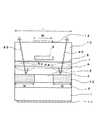
図14は本発明の半導体発光素子を用いた第5実施形態のLEDランプ110を示している。
【0140】
このLEDランプ110は、本発明が適用された半導体発光素子(チップ)114と、この半導体発光素子114を搭載した第1のリード113と、第1のリード113から離間して配置された第2のリード112とを備えている。半導体発光素子114の裏面(n側電極11)は第1のリード113先端に銀ペースト等の導電性接着剤を介して接合されている。半導体発光素子114のp側電極12は金属ワイヤ116によって第2のリード112の先端に接続されている。そして、半導体発光素子114と、第1のリード113、第2のリード112のうち先端近傍の部分とが、エポキシ樹脂等からなる透明の樹脂115で封止されている。樹脂115の先端部は、半導体発光素子114から表面(p側電極12)側へ出た光を効率よく前方に放射させるように、半球状のレンズに加工されている。しかも、半導体発光素子114は従来の半導体発光素子に比して高い輝度を示す。したがって、このLEDランプは高い光度を示すことができる。
【0141】
既述のように、半導体発光素子114は活性層と基板との間に光反射層を有しているので、チップの側面からの放射光が少ない。したがって、半導体発光素子114を搭載したリード113の先端は図のように反射板を設けた形状にされなくても、高い光度を実現できる。
【0142】
なお、活性層の材料が異なり、したがって、発光波長の異なる複数の半導体発光素子を1つのランプに一体に備えても良い。すなわち、第2のリード112を半導体発光素子の数の分だけ設ける。そのような複数の半導体発光素子を共通の第1のリード113の先端に並べて配置する。各半導体発光素子のp側電極12をそれぞれ対応する第2のリード112にAuワイヤによって接続する。このようにした場合、発光波長の異なる複数の半導体発光素子を独立に通電できる。したがって、白色をはじめ、様々な色で発光する高輝度のLEDランプを実現できる。
【0143】
また、より高い輝度を実現するために図14に示したランプを複数集めて集合ランプとしても良い。このような集合ランプは屋外で用いられる信号機等に適している。特に、高い視認性が要求される船舶の舷灯やブイに用いることができる。
【0144】
また、上述の半導体発光素子をマトリクス状に一体に配置して、LED表示装置としての表示盤120を構成しても良い。このようにした場合、屋外でも視認性の良い表示盤を実現することができる。図15は、そのような表示盤120の電気回路を示している。ここで、LED11、LED12、…、LED33は本発明が適用された半導体発光素子を表している。各LED11、LED12、…、LED33には、それぞれ対応するLEDの静電破壊を防ぐための保護ダイオードZ11、Z12、…、Z33が並列に接続されている。また、TR1・・・TR6はLED駆動用のトランジスタである。
【0145】
この例では、LEDと保護ダイオードとは1つのLEDランプとしてそれぞれ一体に構成されている。なお、LEDは一つに限定されることはなく、複数のLEDであっても良い。その場合、複数のLEDおよび保護ダイオードはすべて並列に接続される。さらに、複数のLEDは発光波長が同じであっても良く、そうすることにより輝度を更に高くすることができる。
【0146】
この表示盤120は次のように動作する。例えば、LED22を点灯させたいときは、そのLED22に対して行方向につながるトランジスタTR2と列方向につながるトランジスタTR5とをONすれば良い。このとき、保護ダイオードが単方向のダイオードであると、図のような経路A1を辿って電流が流れて、LED11、12、21も誤点灯することが有る。このため、保護ダイオードとしては双方向性のもの、つまり電圧の向きによらず順電圧が所定の値を超えないと電流が流れないものが望ましい。
【0147】
点灯させるLEDは任意に選ぶことができる。点灯させるLEDは一つに限らず複数であっても良い。
【0148】
【発明の効果】
以上より明らかなように、この発明の半導体発光素子によれば、光反射層のペア数が少なくても反射率が高く、活性層から放出された光を有効に外部に取り出すことができる。
【0149】
また、この発明の半導体発光素子の製造方法によれば、そのような半導体発光素子を量産性良く作製できる。
【0150】
また、この発明のLEDランプ、LED表示装置は高い輝度を示すことができる。
【図面の簡単な説明】
【図1】 本発明の第1の原理を説明する図である。
【図2】 上記第1の原理による光反射層の反射スペクトルを示す図である。
【図3】 本発明の第2の原理を説明する図である。
【図4】 上記第2の原理による光反射層の反射スペクトルを示す図である。
【図5】 本発明による光反射層の反射率のペア数依存性を示す図である。
【図6】 本発明の第1実施形態の発光ダイオードの構成を示す断面図である。
【図7】 本発明の第2実施形態の発光ダイオードの構成を示す断面図である。
【図8】参考例の発光ダイオードの構成を示す断面図である。
【図9】 本発明の第4実施形態の発光ダイオードの構成を示す断面図である。
【図10】 比較例の発光ダイオードを示す断面図である。
【図11】 従来例の発光ダイオードの構成を示す断面図である。
【図12】 別の従来例の発光ダイオードの構成を示す断面図である。
【図13】 従来例の発光ダイオードにおける光反射層の反射率のペア数依存性を示す図である。
【図14】 本発明の半導体発光素子を用いて構成されたLEDランプを示す図である。
【図15】 本発明の半導体発光素子を用いて構成された表示盤を示す図である。
【符号の説明】
1 n型GaAs基板
2 n型GaAsバッファ層
3 n型AlAS電導層
4 n型AlInP/(AlxGa1−x)vIn1−vP光反射層
5 n型AlInPクラッド層
6 p型(AlxGa1−x)vIn1−vP活性層
7 p型AlInPクラッド層
8 p型(AlxGa1−x)vIn1−vP中間層
9 p型GaP電流阻止層
10 p型(AlxGa1−x)vIn1−vP電流拡散層
11 n型電極
12 p型電極
13 AlOy酸化層
14 AlOy/ AlxGa1−xAs酸化光反射層
15 n型AlAs/AlxGa1−xAs電導型光反射層
16 n型AlAs電導層
17 空間領域[0001]
BACKGROUND OF THE INVENTION
The present invention relates to a semiconductor light-emitting element such as a light-emitting diode used for display and optical communication, and a method for manufacturing the same. Moreover, it is related with the LED lamp and LED display apparatus provided with such a semiconductor light-emitting device.
[0002]
[Prior art]
In recent years, high-intensity light-emitting diodes (LEDs) that emit light having wavelengths from infrared to blue have been developed. This is because the crystal growth technique of the direct transition type III-V compound semiconductor material has been dramatically improved, and almost all crystals can be grown if it is a III-V group compound semiconductor. Since LEDs using these direct transition materials can emit light with high output and high brightness, display light sources such as high-intensity LED lamps such as outdoor display boards, low power consumption display lamps, and the like It has come to be widely used as a light source for optical transmission and optical communication using a plastic optical fiber.
[0003]
A light emitting diode using an AlGaInP-based material as shown in FIG. 11 is known as a new high output / high luminance light emitting diode of this type. This light emitting diode is manufactured as follows. That is,
On the n-
an n-type
n-type (AlxGa1-x)0.51In0.49P (x = 0.45) and n-type Al0.51In0.49Distributed feedback type light reflecting layer (
n-type (AlxGa1-x)0.51In0.49P lower cladding layer (0 ≦ x ≦ 1, for example, x = 1.0, thickness 1.0 μm,
p-type (AlxGa1-x)0.51In0.49P active layer (0 ≦ x ≦ 1, for example, x = 0.42, thickness 0.6 μm,
p-type (AlxGa1-x)0.51In0.49P upper cladding layer (0 ≦ x ≦ 1, for example x = 1.0, thickness 1.0 μm,
Are stacked one after another
p-type (AlxGa1-x)vIn1-vP intermediate layer (x = 0.2, v = 0.4, thickness 0.15 μm,
p-type (AlxGa1-x)vIn1-vP current diffusion layer (x = 0.05, v = 0.05, thickness 1.5 μm,
n-type GaP current blocking layer (thickness 0.3 μm,
[0004]
Thereafter, selective etching by a normal photolithography method is performed to leave a portion of the n-type GaP
[0005]
Finally, for example, an Au—Be film is deposited on the p-type
[0006]
Hereinafter, for the sake of simplicity, the ratio x of Al to Ga, the ratio v of other Group III elements when Al and Ga are combined, and the like will be omitted as appropriate.
[0007]
As described above, the p-type AlGaInP
[0008]
(AlxGa1-x)vIn1-vAs the substrate for the P-based light emitting diode, a GaAs substrate is usually used so as to lattice match with the material of each layer. However, the band gap of the GaAs substrate is 1.42 eV (AlxGa1-x)vIn1-vSmaller than that of P-based semiconductors, hence (AlxGa1-x)vIn1-vSince light of 550 nm to 670 nm which is the emission wavelength of the P-based semiconductor is absorbed, light emitted from the active layer is absorbed inside the chip and cannot be extracted outside. . Therefore, (AlxGa1-x)vIn1-vIn order to fabricate a light-emitting diode with high efficiency and high brightness in a P-based light emitting diode, a layer having a small refractive index and a layer having a large refractive index are provided between the
[0009]
As is well known, the optical film thickness is given by nd, where d is the crystal layer thickness and n is the refractive index.
[0010]
(AlxGa1-x)vIn1-vIn a P-based light emitting diode, as shown in FIG.xGa1-xA
[0011]
[Problems to be solved by the invention]
By the way, as can be seen from FIGS. 13A and 13B, in order to obtain a high reflectance of 90% or more that can improve the luminous intensity by a factor of 2 or more, the number of semiconductor layer pairs constituting the
[0012]
However, if the number of pairs is 30 or more, the growth time becomes long and the mass productivity becomes poor. Also, if the difference in refractive index is small, the half width of the reflection spectrum will be narrowed, and the reflection spectrum will be greatly shifted by a slight change in the thickness of the light reflection layer, so the emission wavelength and the light reflection layer must be matched. Becomes difficult, and reproducibility, and hence mass productivity, is poor. Further, when the number of pairs increases, the light reflection layer alone becomes a thick film of 3 μm or more, and the substrate after epitaxial growth is warped or easily deformed, making it difficult to perform subsequent steps.
[0013]
This situation is not limited to the AlGaInP-based material, and the same applies to semiconductor light emitting devices using various other materials.
[0014]
Accordingly, an object of the present invention is to provide a semiconductor light emitting device capable of effectively extracting light emitted from an active layer to the outside.
[0015]
Moreover, the subject of this invention is providing the manufacturing method of the semiconductor light-emitting device which can produce such a semiconductor light-emitting device with sufficient mass productivity.
[0016]
Moreover, the subject of this invention is providing the LED lamp and LED display apparatus provided with such a semiconductor light-emitting device.
[0017]
[Means for Solving the Problems]
In order to solve the above problems, the semiconductor light emitting device of the present invention is configured as follows. That is, the semiconductor light emitting device of the present invention is
In a semiconductor light emitting device in which a plurality of layers including an active layer made of a semiconductor that generates light of a predetermined wavelength are stacked on a semiconductor substrate,
Between the semiconductor substrate and the active layer, a sub-reflective portion made of a semiconductor layer containing Al and a dielectric containing AlBodyAnd a first light reflection layer having a main reflection portion having a higher reflectance with respect to light from the active layer than the sub-reflection portion.,
The semiconductor substrate is of a first conductivity type;
A second conductivity type current spreading layer is provided on the active layer;
A current blocking layer of a first conductivity type provided in a predetermined region inside the current spreading layer;
An electrode layer provided in a region corresponding to the current blocking layer on the upper surface of the current spreading layer,
The sub-reflective portion of the first light reflecting layer is disposed in a region corresponding to the current blocking layer,
The main reflection portion of the first light reflection layer is disposed in a region corresponding to the periphery of the current blocking layer.It is characterized by that.
[0018]
In the semiconductor light emitting device of the present invention, a sub-reflection portion composed of a semiconductor layer containing Al and a dielectric containing Al between the semiconductor substrate and the active layer.BodyAnd a first light reflection layer having a main reflection portion having a higher reflectance with respect to light from the active layer than the sub-reflection portion, which is continuous in the layer direction. Therefore, the light emitted from the active layer is reflected with high reflectance by the main reflection portion of the first light reflection layer. If the main reflection portion of the first light reflection layer is disposed in a necessary region, for example, a region where no electrode is present on the active layer, the light emitted from the active layer is reflected by the main reflection portion of the first light reflection layer. The light is emitted to the outside without being blocked by the electrode. Therefore, the light emitted from the active layer can be effectively extracted outside.
[0019]
Further, in this semiconductor light emitting device, the conduction current injected from the electrode layer into the current diffusion layer is blocked by the current blocking layer provided in a predetermined region inside the current diffusion layer, and the region around the current blocking layer A lot flows. As a result, a large portion of the active layer corresponding to the periphery of the current blocking layer emits light. Since the main reflection portion of the first light reflection layer is disposed in the region corresponding to the periphery of the current blocking layer, the light emitted from the portion corresponding to the periphery of the current blocking layer in the active layer is the first. The light is reflected by the main reflection portion of the
[0020]
In one embodiment, the semiconductor light emitting device includes a pair of a low refractive index material layer and a high refractive index material layer so as to reflect light from the active layer between the first light reflecting layer and the active layer. A second light reflecting layer formed by laminating a plurality of layers is provided.
[0021]
In the semiconductor light emitting device of this embodiment, the low refractive index material layer and the high refractive index material layer are arranged between the first light reflection layer and the active layer so as to reflect light from the active layer. Since the second light reflecting layer formed by laminating a plurality of pairs is provided, the light emitted from the active layer can be extracted more effectively to the outside. The main reflection portion of the first light reflection layer is a dielectric containing Al.Consist ofTherefore, the refractive index n is lower than that of the sub-reflection portion made of a semiconductor layer containing Al. Since the refractive index n of the main reflection part of the first light reflection layer is low, the number of pairs of the second light reflection layer is at least high in reflectance.
[0022]
The second light reflecting layer is preferably a distributed feedback light reflecting layer (DBR).
[0023]
In the semiconductor light emitting device of one embodiment, the sub-reflection portion of the first light reflection layer is made of Al.xGa1-xAs, (AlxGa1-x)vIn1-vP, (AlxGa1-x)vIn1-vN, (AlxGa1-x)vIn1-vAs, (AlxGa1-x)vIn1-vIt is made of any one kind of semiconductors among Sb (where 0 <x ≦ 1, 0 <v <1). The main reflection portion of the first light reflection layer is AlO.y(However, y is a positive real number.OrIt becomes.
[0024]
In this specification, the notation of aluminum oxide is AlO.yTo unify. AlOyIs AlxOy(Where x and y are positive real numbers).
[0025]
In addition, x, v, y, etc. which represent a composition shall take an independent value between different compounds.
[0026]
In one embodiment, the sub-reflection portion of the first light reflection layer is made of Al.xGa1-xAs layer and AlzGa1-zA multilayer film in which As layers are alternately stacked, (AlxGa1-x)vIn1-vP layer and (AlzGa1-z)vIn1-vA multilayer film in which P layers are alternately stacked, (AlxGa1-x)vIn1-vN layer and (AlzGa1-z)vIn1-vA multilayer film in which N layers are alternately stacked, (AlxGa1-x)vIn1-vAs layer and (AlzGa1-z)vIn1-vA multilayer film in which As layers are alternately stacked, (AlxGa1-x)vIn1-vSb layer and (AlzGa1-z)vIn1-vThe multilayer film is composed of any one of the multilayer films in which Sb layers are alternately stacked (where 0 <x <z ≦ 1 and 0 <v <1). The main reflection portion of the first light reflection layer is Al corresponding to the multilayer film forming the sub-reflection portion.xGa1-xAs, (AlxGa1-x)vIn1-vP, (AlxGa1-x)vIn1-vN, (AlxGa1-x)vIn1-vAs, (AlxGa1-x)vIn1-vAny one of Sb (where 0 <x ≦ 1, 0 <v <1) and AlOyLayer (where y is a positive real number).)WhenIt consists of what laminated | stacked alternately.
[0027]
Now, as described with respect to the prior art, in order to increase the light extraction efficiency by obtaining a high reflectivity by the light reflection layer and achieve high brightness and high output, the light reflection layer is a single layer. For this, it is necessary to increase the difference in refractive index between the two layers sandwiching the reflecting surface of the light reflecting layer. Further, when the light reflecting layer is formed of a multilayer film, the difference in refractive index between the pair of semiconductor films constituting the light reflecting layer must be increased. But for example (AlxGa1-x)vIn1-vIn the case of a P-based light emitting diode, any material system that does not absorb light and lattice-matches to the active layer is a compound semiconductor material (AlxGa1-x)vIn1-vP or AlxGa1-xIt is limited to the As system, and the refractive index can be changed only within a range of about 2.9 to 3.5.
[0028]
On the other hand, the principle diagram of the reflective layer of the present invention is shown in FIG. AlOy oxide layer b obtained by oxidizing AlAs on semiconductor substrate a, AlxGa1-xIn this structure, an As layer, a light reflection layer c formed by alternately laminating a high refractive index semiconductor material and a low refractive index semiconductor material, and an active layer d are deposited in this order. On the other hand, there was no AlOy oxide layer b conventionally. In this case, the light reflection layer c and AlOyA large refractive index difference of about 0.6 to 1.4 can be provided between the layer b and the layer b. Therefore, the light reflection layer c and AlOyThe reflectivity at the interface with the layer b is increased, and a greater reflectivity than that of a normal light reflecting layer can be obtained. For example, as shown in FIG. 2, according to the present invention, AlOyCompared with the case where no layer is provided (conventional), the reflectance is high, and the half width of the reflection spectrum can be increased (the wavelength range with high reflectance is wide).
[0029]
On the other hand, FIG. 3 shows a principle diagram of another reflective layer of the present invention. On the semiconductor substrate a, an AlAs layer and AlxGa1-xAs layers are alternately stacked, and the AlAs layer is formed of AlO.yIt is a structure in which a light reflecting layer f and an active layer d, which are changed to a layer (where y is a positive real number) b, are deposited in this order. Conventional AlAs layer and AlxGa1-xCompared to the light-reflective layer in which As layers are alternately stacked, AlOyLayer and AlxGa1-xThe refractive index difference between the As layer and the As layer can be as large as about 0.6 to 1.4. As a result, the reflection characteristic of the light reflection layer f has a maximum reflectance as high as 99% as shown in FIG. 4, and its wavelength range is also widened. Furthermore, the reflectance of the light having a wavelength outside the required wavelength range is abruptly reduced, so that the color purity of the semiconductor light emitting element is increased. Similar to the case of FIG. 1, even if the layer thickness varies or fluctuates, the reflectance and the reflection spectrum hardly change, and the mass productivity is excellent.
[0030]
Since Al has a strong bond with oxygen, it has a property of being easily oxidized, and an Al oxide is formed only by leaving it in the atmosphere. However, the Al oxide film that has been naturally oxidized in this way has poor characteristics such as many holes in the film. Thus, for example, AlxGa1-xWhen an As layer (especially one having an Al mixed crystal ratio x close to 1) is left in a water vapor atmosphere at a temperature of 300 ° C. to 400 ° C., it is oxidized by high temperature water vapor, and more stable AlO.yA layer can be formed (for example, US Pat. No. 5,517,039, or Kenichi Iga et al., “Basics and Applications of Surface Emitting Lasers”, Kyoritsu Shuppan Co., Ltd., June 1999, p. 105). -113). This AlOySince the layer is an oxide (dielectric), the refractive index n is extremely lower than that of the semiconductor material, and takes a value of n = 2.5 to 1.9. Therefore, the above AlxGa1-xAs layer is AlOyBy changing the refractive index by changing the layer, the reflectance of the light emitted from the active layer can be increased. Therefore, even if the number of pairs of light reflecting layers is small, the reflectance is high, and the light emitted from the active layer can be effectively extracted outside.
[0031]
AlOySince the layer is an oxide (dielectric), it has a large band gap and is transparent to the visible light region from blue to red. Therefore, according to the present invention, it is possible to form a high-quality light reflecting layer that has extremely small wavelength dependency and a reflectance close to 100%. Therefore, there is no need to bother selecting an Al composition that does not absorb the emission wavelength, unlike a light reflecting layer made of a conventional semiconductor material.
[0032]
According to the present invention, AlOyCompared with the case where no layer is provided (conventional), the reflectance is high, and the half width of the reflection spectrum can be increased. As a result, even if there are variations or fluctuations in the thickness of the light reflection layer, the reflectance and the reflection spectrum are unlikely to change. Therefore, it is excellent in mass productivity.
[0033]
Low refractive index Al-rich layer f constituting the light reflecting layer2Is even lower refractive index AlOySince it becomes a layer, the reflectance with respect to the light which the said active layer emitted can be raised. Therefore, even if the number of pairs of light reflecting layers is small, the reflectance is high, and the light emitted from the active layer can be effectively extracted outside. For example, as shown in FIG. 4, according to the present invention, AlOyCompared with the case where the layer is not changed (conventional), the reflectance is high, and the half-value width of the reflection spectrum can be increased. As a result, even if there are variations or fluctuations in the thickness of the light reflection layer, the reflectance and the reflection spectrum are unlikely to change. Therefore, it is excellent in mass productivity.
[0034]
FIG. 5 shows the dependence of the reflectance of the light reflecting layer according to the present invention on the number of pairs in comparison with the conventional example. In the figure, the solid line α connecting the marks ● represents AlO having a low refractive index according to the present invention.yLayer and high refractive index Al0.60Ga0.40The characteristic at the time of using a pair with an As layer is shown. The other lines β1, β2, β3, β4, β5 show the characteristics when a known pair is used. Specifically, β1 is Al0.75Ga0.25Pair of As layer and AlAs layer, β2 is Al0.70Ga0.30Pair of As layer and AlAs layer, β3 is Al0.60Ga0.40Pair of As layer and AlAs layer, β4 is (Al0.40Ga0.60)0.51In0.49P layer and Al0.51In0.49Pair with P layer, β5 (Al0.50Ga0.50)0.51In0.49P layer and Al0.51In0.49The characteristics when a pair with a P layer is used are shown. As can be seen from the figure, according to the present invention, since the light reflection layer has a large difference in refractive index, even with several pairs of light reflection layers, a reflectance close to 100% is obtained. Therefore, the growth time can be shortened and the mass productivity is high.
[0035]
The method for manufacturing a semiconductor light emitting device of the present invention is configured as follows. That is, the method for manufacturing a semiconductor light emitting device of the present invention is a method for manufacturing a semiconductor light emitting device for producing the semiconductor light emitting device of the present invention. And
Providing an Al-rich layer having a higher Al ratio than the other layers of the plurality of layers between the semiconductor substrate and the active layer;
Dividing the wafer in which the plurality of layers are laminated into chips, and exposing the side surfaces of the Al-rich layer;
The Al contained in the Al-rich layer is oxidized from the exposed side surface, and the peripheral portion of the Al-rich layer is AlO.yThe resulting AlOyA layer as the main reflection portion, while the remaining portion of the Al-rich layer as the sub-reflection portion;
Have
[0036]
According to the method for manufacturing a semiconductor light emitting device of the present invention, the peripheral portion of the Al rich layer is formed of AlO.yBy changing to a layer (dielectric) and lowering the refractive index, the reflectance with respect to the light emitted from the active layer can be increased. Therefore, the light emitted from the active layer can be effectively extracted outside.
[0037]
In one embodiment of the method for manufacturing a semiconductor light emitting device, the step of oxidizing Al contained in the Al-rich layer is performed by leaving the chip with the side surface of the Al-rich layer exposed in water vapor. .
[0038]
In one embodiment of the method for manufacturing a semiconductor light emitting device, the water vapor is introduced into a side surface of the Al-rich layer by an inert gas (Ar, nitrogen, etc.) passed through boiling water.
[0039]
In one embodiment of the method for manufacturing a semiconductor light emitting device, the step of oxidizing Al contained in the Al-rich layer is performed in an atmosphere at a temperature of 300 ° C. to 400 ° C.
[0040]
In addition,The AlO generated in the peripheral portion of the Al-rich layeryRemoving the layer by etchingMay have.
[0041]
If you do soAlOySince the refractive index of the spatial region generated by removing the layer is 1, a state close to total reflection is obtained in the chip peripheral region on the back side of the active layer. Therefore, the light emitted from the active layer can be effectively extracted outside.
[0042]
In addition, the LED lamp of the present invention includes the semiconductor light emitting device of the present invention.
[0043]
The LED lamp of one embodiment is characterized in that a plurality of semiconductor light emitting elements having different wavelengths are integrally provided as the semiconductor light emitting elements, and these semiconductor light emitting elements are connected so as to be energized independently.
[0044]
The LED display device of the present invention is characterized in that such LED lamps are arranged in a matrix.
[0045]
In one embodiment of the method for manufacturing a semiconductor light emitting device, the AlO layer among the Al rich layers.yAn electrode for energization is formed in a region on the active layer corresponding to the remaining portion that is not changed into a layer.
[0046]
In the method of manufacturing a semiconductor light emitting device according to the embodiment, the AlO layer is included in the Al rich layer.yAn electrode is formed in a region on the active layer corresponding to the remaining portion that is not changed into a layer. Therefore, the AlO of the Al rich layeryIt can be avoided that the electrode occupies a region corresponding to the changed part of the layer. Therefore, the AlO is generated in the active layer.yThe light reflected by the layer is effectively extracted outside without being blocked by the electrode.
[0047]
In one embodiment of the method for manufacturing a semiconductor light emitting device, the AlO layer among the Al rich layers.yIt is characterized in that a current blocking layer that prevents an energized current is formed in a region corresponding to the remaining portion that is not changed into a layer.
[0048]
In the method of manufacturing a semiconductor light emitting device according to the embodiment, the AlO layer is included in the Al rich layer.yIn the region corresponding to the remaining portion that is not changed to the layer, a current blocking layer that prevents the energized current is formed. Therefore, compared with the case where the current blocking layer is not formed, the AlOyA large amount of energizing current flows in the region corresponding to the layer. Therefore, the AlO is generated in the active layer.yThe light reflected by the layer is effectively extracted outside.
[0049]
In one embodiment of the method for manufacturing a semiconductor light emitting device, the light reflecting layer includes an AlO layer having a predetermined Al mixed crystal ratio and AlO.yConsisting of alternating layers with layers, the AlOyThe thickness of one of the layers constituting the light reflection layer adjacent to the layer containing Al changed into the layer is set to ¼ of the wavelength.
[0050]
In one embodiment of the method for manufacturing a semiconductor light emitting device, after dividing each layer into chips, the AlO layer is exposed from the end face where the Al rich layer is exposed.yThe AlO layer in the Al-rich layer.yThe shape of the remaining portion that is not changed into a layer is made to coincide with the shape of the electrode on the active layer.
[0051]
According to the method for manufacturing a semiconductor light emitting device of this embodiment, there is no need to bother selecting an Al composition that does not absorb the emission wavelength, unlike a light reflecting layer made of a conventional semiconductor material.
[0052]
From another aspect, the semiconductor light-emitting device according to the present invention is a semiconductor light-emitting device having a light-emitting layer that generates light having a predetermined wavelength on a semiconductor substrate, wherein the light-emitting element is interposed between the semiconductor substrate and the light-emitting layer. A semiconductor layer having a refractive index changing in the layer direction is provided so as to reflect light emitted from the layer.
[0053]
Here, the “layer direction” means a direction along the layer, that is, a direction in which the layer spreads (plane direction).
[0054]
In the semiconductor light emitting device of the present invention, a semiconductor layer whose refractive index is changed in the layer direction is provided between the semiconductor substrate and the light emitting layer so as to reflect the light emitted from the light emitting layer. By reducing the refractive index in a region where the refractive index of the semiconductor layer is necessary, for example, in a region where no electrode is present on the light emitting layer, the reflectance of the light emitted from the light emitting layer can be increased. Therefore, even if the number of pairs of light reflecting layers is small, the reflectance is high, and the light emitted from the light emitting layer can be effectively extracted outside.
[0055]
As described above, in order to obtain a high reflectivity by the light reflection layer, increase the light extraction efficiency, and achieve high luminance and high output, a pair of semiconductor films constituting the light reflection layer is formed. The refractive index difference must be increased. But for example (AlxGa1-x)vIn1-vIn the case of P-based light emitting diodes, any material system that does not absorb light and lattice matches with the light emitting layer is a compound semiconductor material (AlxGa1-x)vIn1-vP or AlxGa1-xIt is limited to the As system, and the refractive index can be changed only within a range of about 2.9 to 3.5.
[0056]
Therefore, in the method for manufacturing a semiconductor light emitting device of the present invention, in the method for manufacturing a semiconductor light emitting device in which a light emitting layer that generates light having a predetermined wavelength is provided on a semiconductor substrate, AlxGa1-xThe As layer and the light-emitting layer are deposited in this order, and the Al direction with respect to the layer direction is deposited.xGa1-xPart of the As layer is made of AlOyIt is characterized by changing to a layer (where y is a positive real number).
[0057]
AlxGa1-xSince Al in the As layer has a strong bond with oxygen, it is very easily oxidized, and when left in the atmosphere, an Al oxide is formed. Therefore, AlxGa1-xWhen an As layer (especially one having an Al mixed crystal ratio x close to 1) is oxidized in water vapor at a temperature of 300 ° C. to 400 ° C., stable AlOyA layer is formed. This AlOySince the layer is an oxide containing Al, the refractive index n is extremely lower than that of the semiconductor material, and takes a value of n = 2.5 to 1.9. Therefore, the above AlxGa1-xAs layer is AlOyBy changing the refractive index by changing the layer, the reflectance of the light emitted from the light emitting layer can be increased. Therefore, even if the number of pairs of light reflecting layers is small, the reflectance is high, and the light emitted from the light emitting layer can be effectively extracted outside.
[0058]
AlOySince the layer is an oxide, the band gap is large, and the visible light region, particularly (AlxGa1-x)vIn1-vIt is transparent with respect to 560 nm to 650 nm which is a P-based light emitting region. Therefore, according to the present invention, it is possible to form a high-quality light reflecting layer that has extremely small wavelength dependency and a reflectance close to 100%. Therefore, there is no need to bother selecting an Al composition that does not absorb the emission wavelength, unlike a light reflecting layer made of a conventional semiconductor material.
[0059]
In the method of manufacturing a semiconductor light emitting device according to one embodiment, as illustrated in FIG.xGa1-xAn As layer, a light reflection layer c formed by alternately laminating a high refractive index semiconductor material and a low refractive index semiconductor material, and a light emitting layer d are deposited in this order.xGa1-xPart of the As layer is made of AlOyChange to layer b (however, in FIG. 1 AlOyOnly the changed areas in the layers are shown. ). In this case, the light reflection layer c and AlOyA large refractive index difference of about 0.6 to 1.4 can be provided between the layer b and the layer b. Therefore, the light reflection layer c and AlOyThe reflectivity at the interface with the layer b is increased, and a greater reflectivity than that of a normal light reflecting layer can be obtained. For example, as shown in FIG. 2, according to the present invention, AlOyCompared with the case where no layer is provided (conventional), the reflectance is high, and the half width of the reflection spectrum can be increased. As a result, even if there are variations or fluctuations in the thickness of the light reflection layer, the reflectance and the reflection spectrum are unlikely to change. Therefore, it is excellent in mass productivity.
[0060]
In the method for manufacturing a semiconductor light emitting device according to one embodiment, as illustrated in FIG. 3, a semiconductor material f having a high refractive index is formed on a semiconductor substrate a.1And low refractive index AlxGa1-xAs layer f2(However, 0 <x ≦ 1.) The light reflecting layer f and the light emitting layer d, which are alternately stacked, are deposited in this order, and the above-described Al in the layer direction is deposited.xGa1-xAs layer f2A part of AlOy(In FIG. 3, AlOyOnly the region (stipple) changed to the layer is shown. ). In this case, the low refractive index Al constituting the light reflecting layerxGa1-xAs layer f2AlO with a lower refractive index layerySince it becomes a layer, the reflectance with respect to the light which the said light emitting layer emitted can be raised. Therefore, even if the number of pairs of light reflecting layers is small, the reflectance is high, and the light emitted from the light emitting layer can be effectively extracted outside. For example, as shown in FIG. 4, according to the present invention, AlOyCompared with the case where the layer is not changed (conventional), the reflectance is high, and the half-value width of the reflection spectrum can be increased. As a result, even if there are variations or fluctuations in the thickness of the light reflection layer, the reflectance and the reflection spectrum are unlikely to change. Therefore, it is excellent in mass productivity.
[0061]
FIG. 5 shows the dependence of the reflectance of the light reflecting layer according to the present invention on the number of pairs in comparison with the conventional example. According to the present invention, since the light reflection layer has a large refractive index difference, a reflectance close to 100% can be obtained even with several pairs of light reflection layers. Therefore, the growth time can be shortened and the mass productivity is high.
[0062]
In one embodiment of a method for manufacturing a semiconductor light emitting device, the AlxGa1-xA part of the As layer is AlOyAfter changing to a layer, its AlOyThe layer is removed.
[0063]
In the method for manufacturing a semiconductor light emitting device of this embodiment, AlOySince the refractive index of the spatial region generated by removing the layer is 1, a state close to total reflection is obtained in the chip peripheral region on the back side of the light emitting layer. Therefore, the light emitted from the light emitting layer can be effectively extracted outside.
[0064]
In one embodiment of the method of manufacturing a semiconductor light emitting device, the AlxGa1-xOf the As layer, the above AlOyAn electrode for energization is formed in a region on the light emitting layer corresponding to the remaining portion which is not changed into a layer.
[0065]
In the method of manufacturing a semiconductor light emitting device according to this embodiment, the AlxGa1-xOf the As layer, the above AlOyAn electrode is formed in a region on the light emitting layer corresponding to the remaining portion that is not changed into a layer. Therefore, the above AlxGa1-xOf the As layer, the above AlOyIt can be avoided that the electrode occupies a region corresponding to the changed part of the layer. Therefore, the AlO is generated in the light emitting layer.yThe light reflected by the layer is effectively extracted outside without being blocked by the electrode.
[0066]
In one embodiment of the method of manufacturing a semiconductor light emitting device, the AlxGa1-xOf the As layer, the above AlOyIt is characterized in that a current blocking layer that prevents an energized current is formed in a region corresponding to the remaining portion that is not changed into a layer.
[0067]
In the method of manufacturing a semiconductor light emitting device according to this embodiment, the AlxGa1-xOf the As layer, the above AlOyIn the region corresponding to the remaining portion that is not changed to the layer, a current blocking layer that prevents the energized current is formed. Therefore, compared with the case where the current blocking layer is not formed, the AlOyA large amount of energizing current flows in the region corresponding to the layer. Therefore, the AlO is generated in the light emitting layer.yThe light reflected by the layer is effectively extracted outside.
[0068]
In one embodiment of the method for manufacturing a semiconductor light emitting device, the light reflecting layer is made of Al having a predetermined Al mixed crystal ratio.xGa1-xAs layer (where 0 <x ≦ 1) and AlOyConsisting of alternating layers with layers, the AlOyAl changed to layerxGa1-xAl forming the light reflecting layer adjacent to the As layerxGa1-xThe thickness of one layer of the As layer is set to ¼ of the wavelength.
[0069]
According to the method for manufacturing a semiconductor light emitting device of this embodiment, the AlOyIn the region corresponding to the layer, the reflectance with respect to the light emitted from the light emitting layer is further increased.
[0070]
In one embodiment of the method for manufacturing a semiconductor light emitting device, the light emitting layer is made of (AlxGa1-x)vIn1-vA method for manufacturing a semiconductor light emitting device, comprising forming a P-based material.
[0071]
According to the method for manufacturing a semiconductor light emitting device of this embodiment, a semiconductor light emitting device having an emission wavelength band of 560 nm to 650 nm is manufactured.
[0072]
In the method of manufacturing a semiconductor light emitting device according to one embodiment, after each of the layers is divided into chips, the AlxGa1-xFrom the end face where the As layer is exposed, the AlOyChange the layer to the above AlxGa1-xOf the As layer, the above AlOyThe shape of the remaining part which is not changed into the layer is made to coincide with the shape of the electrode on the light emitting layer.
[0073]
In the method of manufacturing a semiconductor light emitting device according to this embodiment, the AlxGa1-xFrom the end face where the As layer is exposed, the AlOyAlO changes to the layeryThe layer can be formed stably and easily. Therefore, it is excellent in mass productivity. Moreover, the above AlxGa1-xOf the As layer, the above AlOySince the shape of the remaining portion that is not changed into the layer matches the shape of the electrode on the light emitting layer, the AlxGa1-xOf the As layer, the above AlOyIt can be avoided that the electrode occupies a region corresponding to the changed part of the layer. Therefore, the AlO is generated in the light emitting layer.yThe light reflected by the layer is effectively extracted outside without being blocked by the electrode.
[0074]
In the method of manufacturing a semiconductor light emitting device according to one embodiment, after each of the layers is divided into chips, the AlxGa1-xFrom the end face where the As layer is exposed, the AlOyChange the layer to the above AlxGa1-xOf the As layer, the above AlOyThe shape of the remaining portion that is not changed into the layer is made to coincide with the shape of the current blocking layer.
[0075]
In the method of manufacturing a semiconductor light emitting device according to this embodiment, the AlxGa1-xFrom the end face where the As layer is exposed, the AlOyAlO changes to the layeryThe layer can be formed stably and easily. Therefore, it is excellent in mass productivity. Moreover, the above AlxGa1-xOf the As layer, the above AlOySince the shape of the remaining portion that is not changed into the layer matches the shape of the current blocking layer, the AlOyA large amount of energizing current flows in the region corresponding to the layer. Therefore, the AlO is generated in the light emitting layer.yThe light reflected by the layer is effectively extracted outside.
[0076]
In one embodiment of the method of manufacturing a semiconductor light emitting device, the AlxGa1-xInstead of As layer, AlxGa1-xP layer, AlxIn1-xP layer or AlxIn1-xAn As layer is used.
[0077]
The method for manufacturing a semiconductor light emitting device of the present invention is a method for manufacturing a semiconductor light emitting device in which a light emitting layer for generating light having a predetermined wavelength is provided on a semiconductor substrate. Al withxGa1-xAs layer (where 0 <x ≦ 1) and (AlxGa1-x)vIn1-vA light reflecting layer for reflecting light having the above wavelength and a light emitting layer are deposited in this order, which are composed of alternating layers of P layers (where 0 <x ≦ 1, 0 <v <1). The above Al in the layer directionxGa1-xPart of the As layer is made of AlOyIt is characterized by changing to a layer (where y is a positive real number).
[0078]
According to the method for manufacturing a semiconductor light emitting device of the present invention, the AlxGa1-xAs layer is AlOyBy changing the refractive index by changing the layer, the reflectance of the light emitted from the light emitting layer can be increased. Therefore, even if the number of pairs of light reflecting layers is small, the reflectance is high, and the light emitted from the light emitting layer can be effectively extracted outside.
[0079]
AlOySince the layer is an oxide, the band gap is large, and the visible light region, particularly (AlxGa1-x)vIn1-vIt is transparent with respect to 560 nm to 670 nm which is a P-type light emitting region. Therefore, according to the present invention, it is possible to form a high-quality light reflecting layer that has extremely small wavelength dependency and a reflectance close to 100%. Therefore, there is no need to bother selecting an Al composition that does not absorb the emission wavelength, unlike a light reflecting layer made of a conventional semiconductor material.
[0080]
In one embodiment, a method of manufacturing a semiconductor light emitting device includes the AlxGa1-xPart of the As layer is made of AlOyAfter changing to a layer, its AlOyWhen removing the layer, a hydrofluoric acid-based etchant is used.
[0081]
According to the method for manufacturing a semiconductor light emitting device of this embodiment, the AlOyAl layer onlyxGa1-xIt can be removed by selectively etching the As layer or the like.
[0082]
DETAILED DESCRIPTION OF THE INVENTION
Hereinafter, the present invention will be described in detail with reference to the illustrated embodiments.
[0083]
(First embodiment)
FIG. 6 shows a cross-sectional structure of the semiconductor light emitting diode of the first embodiment. This embodiment is characterized in that the main reflection portion of the first light reflection layer is composed of an AlOy single layer (where y is a positive real number).
[0084]
This light-emitting diode has an n-type GaAs buffer layer (for example, a thickness of 0.5 μm, an impurity concentration of 5 × 10 10) on an n-type GaAs substrate 1.17cm-3) 2, n-type AlAs
[0085]
This light emitting diode is manufactured as follows.
[0086]
i) An n-type GaAs buffer layer (e.g., a thickness of 0.5 μm, an impurity concentration of 5 × 10)17cm-3) 2, n-type AlAs
[0087]
ii) Next, p-type (AlxGa1-x)vIn1-vP-type (AlxGa1-x)vIn1-vP current diffusion layer (x = 0.05, v = 0.05, thickness 1.5 μm,
[0088]
iii) Next, a metal layer to be an electrode is provided on the p side, and the
[0089]
iv) The AlAs
[0090]
Further, there is a feature that a higher quality oxide film can be obtained by oxidizing with water vapor than when simply oxidizing with oxygen. In particular, the reason why water vapor is brought into the thermostatic layer by nitrogen gas is to prevent oxygen from entering.
[0091]
This layer direction dimension N is L for the chip size, M for the length of one side of the current blocking layer or electrode,
N ≦ (LM) / 2
Is desirable. In this embodiment, AlOyThe
[0092]
Further, the exposed AlAs
[0093]
(Comparative example)
FIG. 10 shows a semiconductor light emitting diode having a structure in which the
[0094]
However, in the semiconductor light emitting diode of this comparative example, the effect of improving the luminance was not obtained. The reason is considered as follows. That is, in the semiconductor light emitting diode of this comparative example, there is no current blocking layer immediately below the
[0095]
(Second Embodiment)
FIG. 7 shows a cross-sectional structure of the semiconductor light emitting diode of the second embodiment. This embodiment is characterized in that the main reflection portion of the first light reflection layer is formed of a multilayer film in which a plurality of AlOy layers and AlGaAs layers are alternately stacked.
[0096]
This light-emitting diode has an n-type GaAs buffer layer (for example, a thickness of 0.5 μm, an impurity concentration of 5 × 10 10) on an n-type GaAs substrate 1.17cm-3) 2 and n-type AlAs / Al as a sub-reflective portion provided so as to be continuous in the layer direction as the first light reflecting layerxGa1-xAs conductive light reflecting layer (for example, x = 0.65,
[0097]
This light emitting diode is manufactured as follows.
[0098]
i) An n-type GaAs buffer layer (e.g., a thickness of 0.5 μm, an impurity concentration of 5 × 10)17cm-32) and n-type AlAs / AlxGa1-xAs conductive light reflecting layer (for example, x = 0.65,
[0099]
Where n-type AlAs / AlxGa1-xThe As conductive light reflection layer 15 includes an AlAs layer as an Al-rich layer, an AlAs layer, and an AlAs layer.xGa1-xAs layers are alternately stacked.
[0100]
ii) Next, p-type (AlxGa1-x)vIn1-vP-type (AlxGa1-x)vIn1-vP current diffusion layer (x = 0.05, v = 0.05, thickness 1.5 μm,
[0101]
iii) Next, a metal layer to be an electrode is provided on the p side, and the
[0102]
iv) After this, the side surface of the chip is exposed to the atmosphere, and then n-type AlAs / Al is formed in the same manner as in the first embodiment.xGa1-xEach of the AlAs layers constituting the As conductive light reflecting layer 15 is oxidized from the side edge, and the peripheral portion of the original AlAs layer is made of AlO.yChange to layer. That is, the original n-type AlAs / AlxGa1-xA peripheral portion of the As conductive light reflecting layer 15 is made of AlO as a low refractive material layer.yLayer and Al as high refractive material layerxGa1-xAlO having a structure in which multiple As layers are stacked alternatelyy/ AlxGa1-xThe As oxidized
N ≦ (LM) / 2
Is desirable. In this embodiment, as in the case of the first embodiment, AlOy/ AlxGa1-xThe As-oxidized
[0103]
Thus, the obtained AlOy/ AlxGa1-xThe As oxidized
[0104]
In addition, n-type AlAs / AlxGa1-xWhen each AlAs layer constituting the As conductive light reflection layer 15 is oxidized from the side edge, the distributed feedback
[0105]
(Third embodiment)
Although not shown, the light emitting diode of the third embodiment is characterized in that the material of the first light reflecting layer in the semiconductor light emitting device of the second embodiment shown in FIG. 7 is changed.
[0106]
The light-emitting diode according to this embodiment has an n-type AlInP / (Al as a sub-reflection portion provided so as to be continuous in the layer direction as the first light reflection layer.xGa1-x)vIn1-vP-conducting light reflecting layer and n-type AlOy / (AlxGa1-x)vIn1-vA P-oxidized light reflecting layer is provided. Other elements are the same as those of the semiconductor light emitting device of the second embodiment.
[0107]
Here, n-type AlInP / (AlxGa1-x)vIn1-vThe P-conduction type light reflection layer is a distributed feedback light reflection layer.xGa1-x)vIn1-vA plurality of pairs with the P layer are stacked. AlInP layers constituting each pair, (AlxGa1-x)vIn1-vThe thickness of the P layer is set to be a quarter of the emission wavelength λ.
[0108]
The light emitting diode of this embodiment is manufactured by the same procedure as that of the light emitting diode of the second embodiment. In particular, each n-type AlOy layer included in the main reflection portion of the first light reflection layer is obtained by placing each AlInP layer included in the sub-reflection portion in the oxide film forming apparatus as in the first embodiment. It is formed by oxidation from the side surface of the chip end face. Although the refractive index of the
[0109]
As in this embodiment, when the material to be oxidized is AlInP, the progress of the oxidation is slower than when the material to be oxidized is an AlAs layer. However, if the other material of the pair is GaInP, GaInP is not oxidized at all, and can be oxidized over time. As a result, the controllability of the layer-direction dimension (oxidation depth) N of the oxidized portion is improved. In addition, the half-value width of the reflection spectrum was more than three times larger than the half-value width (about 20 nm) of a normal light reflection layer. Therefore, even when there is a change in the thickness of each layer constituting the first light reflection layer during mass production, the change in reflectance and reflection spectrum is reduced. As a result, the uniformity of luminous intensity was improved and the yield was also improved.
[0110]
(Reference example)
Figure 8Reference example2 shows a cross-sectional structure of the semiconductor light emitting diode. thisReference exampleIs characterized in that the main reflection portion of the first light reflection layer is formed of a space.
[0111]
This light-emitting diode has an n-type GaAs buffer layer (for example, a thickness of 0.5 μm, an impurity concentration of 5 × 10 10) on an n-type GaAs substrate 1.17cm-3) 2, and an n-type AlAs
[0112]
This light emitting diode is manufactured as follows.
[0113]
i) An n-type GaAs buffer layer (e.g., a thickness of 0.5 μm, an impurity concentration of 5 × 10)17cm-3) 2, n-type AlAs
[0114]
ii) Next, p-type (AlxGa1-x)vIn1-vP-type (AlxGa1-x)vIn1-vP current diffusion layer (x = 0.05, v = 0.05, thickness 1.5 μm,
[0115]
iii) Next, a metal layer to be an electrode is provided on the p side, and the
[0116]
iv) Thereafter, after exposing the chip end face to the atmosphere, the AlAs
N ≦ (LM) / 2
Is desirable. BookReference exampleAlOyIt is placed in an oxide film forming apparatus at 400 ° C. for 3 hours so that the layer dimension N of the layer is 80 μm. The refractive index of the original semiconductor layer is 2.9 to 3.5, but AlO obtained by oxidationyThe refractive index of the layer is as low as 1.9.
[0117]
v) BooksReference exampleThen, in order to obtain a lower reflectance, AlO generated in the peripheral portion of the original AlAs
[0118]
As described above, this light emitting diode is formed by oxidizing the AlAs
[0119]
AlOyThe refractive index of the
[0120]
Actually, bookReference exampleThen, the chip luminous intensity at the emission wavelength of 570 nm could be improved from the normal 35 mcd to 60 mcd. In addition, since the main reflection portion of the first light reflection layer is the
[0121]
(4thEmbodiment)
Figure 94th1 shows a cross-sectional structure of a semiconductor light emitting diode according to an embodiment. This embodiment is characterized in that a second light reflection layer is provided between the first light reflection layer and the active layer.
[0122]
This light-emitting diode has an n-type GaAs buffer layer (for example, a thickness of 0.5 μm, an impurity concentration of 5 × 10 10) on an n-type GaAs substrate 1.17cm-3) 2, n-type AlAs
[0123]
This light emitting diode is manufactured as follows.
[0124]
i) An n-type GaAs buffer layer (e.g., a thickness of 0.5 μm, an impurity concentration of 5 × 10)17cm-3) 2, n-type AlAs
[0125]
As already mentioned, n-type AlInP / (AlxGa1-x)vIn1-vThe P
[0126]
ii) Next, p-type (AlxGa1-x)vIn1-vP-type (AlxGa1-x)vIn1-vP current diffusion layer (x = 0.05, v = 0.05, thickness 1.5 μm,
[0127]
iii) Next, a metal layer to be an electrode is provided on the p side, and the
[0128]
iv) Thereafter, after exposing the end surface of the chip to the atmosphere, the AlAs
N ≦ (LM) / 2
Is desirable. In the present embodiment, similar to the first embodiment, AlOyThe
[0129]
In this way, this light emitting diode has AlO as the main reflection part.yAfter forming the first light reflecting layer including the
[0130]
The refractive index of the original AlAs
[0131]
Further, the AlAs
[0132]
In addition, since the first
[0133]
Actually, in this embodiment, the chip luminous intensity at the emission wavelength of 570 nm could be improved from the normal 35 mcd to 60 mcd. In addition, the half-value width of the reflection spectrum was more than three times larger than the half-value width of about 20 nm of a normal light reflecting layer. Therefore, even when the thickness of the
[0134]
In each of the embodiments described above, (AlxGa1-x)vIn1-vAlthough the P-type light emitting diode has been described, the same effect can be obtained with other light-emitting diodes such as AlGaAs-based, InGaAsP-based, InGaAs-based, and GaInN-based light-emitting diodes. AlOyThe material that changes the layer is AlxGa1-xNot limited to As etc., AlxGa1-xP, AlxIn1-xP, AlxIn1-xThe same effect can be obtained with As etc.
[0135]
In the semiconductor light emitting device of each of the embodiments described above, a GaAs substrate having substantially the same lattice constant and (AlxGa1-x)vIn1-vAlthough what has been provided with the P active layer has been described, the present invention is also applicable to cases with other materials.
[0136]
For example, sapphire is used for the substrate, and the active layer is (AlwGa1-w)vIn1-vIn the case of N, (AlxGa1-x)vIn1-vN may be used. Also, (AlxGa1-x)vIn1-vN / (AlzGa1-z)vIn1-vAn N semiconductor multilayer film can also be used. However, 0 <w <z <x ≦ 1 and 0 <v <1. The conditions for oxidizing the AlGaInN film may be changed as appropriate. This is because the sapphire of the substrate and the active layer (AlwGa1-w)vIn1-vThis is because the lattice constant is completely different from N, but in the normal chip size range, the properties of the crystal thin film formed on the substrate are substantially the same as those in the case of lattice matching with the substrate.
[0137]
Furthermore, Si or GaN may be used for the substrate. Also, the active layer is made of AlxGa1-xAs, (AlxGa1-x)vIn1-vAs, (AlxGa1-x)vIn1-vIt goes without saying that the same effect can be obtained even when Sb or the like is used.
[0138]
(5thEmbodiment)
If the above-described high-luminance semiconductor light-emitting element is integrated with a lens, a high-luminance LED lamp can be obtained.
[0139]
FIG. 14 uses the semiconductor light emitting device of the present invention.
[0140]
The
[0141]
As described above, since the semiconductor
[0142]
Note that a plurality of semiconductor light emitting elements having different active layer materials and different emission wavelengths may be integrally provided in one lamp. That is, as many
[0143]
In order to achieve higher luminance, a plurality of lamps shown in FIG. 14 may be collected to form a collective lamp. Such a collective lamp is suitable for a traffic light used outdoors. In particular, it can be used for ship lights and buoys that require high visibility.
[0144]
Further, the
[0145]
In this example, the LED and the protection diode are each integrally formed as one LED lamp. Note that the number of LEDs is not limited to one, and a plurality of LEDs may be used. In that case, the plurality of LEDs and the protection diode are all connected in parallel. Furthermore, the plurality of LEDs may have the same emission wavelength, and by doing so, the luminance can be further increased.
[0146]
The
[0147]
The LED to be lit can be arbitrarily selected. The number of LEDs to be lit is not limited to one and may be a plurality.
[0148]
【The invention's effect】
As is clear from the above, according to the semiconductor light emitting device of the present invention, even if the number of pairs of light reflecting layers is small, the reflectance is high, and the light emitted from the active layer can be effectively extracted outside.
[0149]
Moreover, according to the method for manufacturing a semiconductor light emitting device of the present invention, such a semiconductor light emitting device can be manufactured with high productivity.
[0150]
Moreover, the LED lamp and LED display device of the present invention can exhibit high luminance.
[Brief description of the drawings]
FIG. 1 is a diagram for explaining a first principle of the present invention.
FIG. 2 is a diagram showing a reflection spectrum of a light reflection layer according to the first principle.
FIG. 3 is a diagram illustrating a second principle of the present invention.
FIG. 4 is a diagram showing a reflection spectrum of a light reflection layer according to the second principle.
FIG. 5 is a graph showing the dependence of the reflectance of the light reflecting layer according to the present invention on the number of pairs.
FIG. 6 is a cross-sectional view showing a configuration of a light emitting diode according to the first embodiment of the present invention.
FIG. 7 is a cross-sectional view showing a configuration of a light emitting diode according to a second embodiment of the present invention.
[Fig. 8]Reference exampleIt is sectional drawing which shows the structure of this light emitting diode.
FIG. 9 shows the present invention.4thIt is sectional drawing which shows the structure of the light emitting diode of embodiment.
FIG. 10 is a cross-sectional view showing a light emitting diode of a comparative example.
FIG. 11 is a cross-sectional view showing a configuration of a conventional light emitting diode.
FIG. 12 is a cross-sectional view showing a configuration of another conventional light emitting diode.
FIG. 13 is a diagram showing the dependence of the reflectance of the light reflecting layer on the number of pairs in a conventional light emitting diode.
FIG. 14 is a view showing an LED lamp configured using the semiconductor light emitting device of the present invention.
FIG. 15 is a view showing a display panel constituted by using the semiconductor light emitting device of the present invention.
[Explanation of symbols]
1 n-type GaAs substrate
2 n-type GaAs buffer layer
3 n-type AlAS conductive layer
4 n-type AlInP / (AlxGa1-x)vIn1-vP light reflection layer
5 n-type AlInP cladding layer
6 p-type (AlxGa1-x)vIn1-vP active layer
7 p-type AlInP cladding layer
8 p-type (AlxGa1-x)vIn1-vP intermediate layer
9 p-type GaP current blocking layer
10 p-type (AlxGa1-x)vIn1-vP current diffusion layer
11 n-type electrode
12 p-type electrode
13 AlOyOxide layer
14 AlOy/ AlxGa1-xAs oxidation light reflection layer
15 n-type AlAs / AlxGa1-xAs conductive light reflection layer
16 n-type AlAs conductive layer
17 Spatial domain
Claims (11)
Translated fromJapanese上記半導体基板と活性層との間に、Alを含む半導体層からなる副反射部分と、Alを含む誘電体からなり、上記副反射部分よりも上記活性層からの光に対する反射率が高い主反射部分とを、層方向に連なって有する第1の光反射層を備え、
上記半導体基板は第1導電型であり、
上記活性層の上に第2導電型の電流拡散層が設けられ、
上記電流拡散層の内部の所定領域に設けられた第1導電型の電流阻止層と、
上記電流拡散層の上部表面で上記電流阻止層に対応する領域に設けられた電極層とを備え、
上記第1の光反射層の副反射部分は上記電流阻止層に対応する領域に配置され、
上記第1の光反射層の主反射部分は上記電流阻止層の周りに対応する領域に配置されていることを特徴とする半導体発光素子。In a semiconductor light emitting device in which a plurality of layers including an active layer made of a semiconductor that generates light of a predetermined wavelength are stacked on a semiconductor substrate,
Between the semiconductor substrate and the active layer, and a sub-reflecting portion composed of semiconductor layer containing Al,dielectric or Rannahli containing Al, the main high reflectance for light from the active layer than the sub reflecting portion A first light reflection layer having a reflection portion connected in the layer direction;
The semiconductor substrate is of a first conductivity type;
A second conductivity type current spreading layer is provided on the active layer;
A current blocking layer of a first conductivity type provided in a predetermined region inside the current spreading layer;
An electrode layer provided in a region corresponding to the current blocking layer on the upper surface of the current spreading layer,
The sub-reflective portion of the first light reflecting layer is disposed in a region corresponding to the current blocking layer,
The semiconductor light emitting element according toclaim 1, wherein a main reflection portion of the first light reflection layer is disposed in a region corresponding to the periphery of the current blocking layer .
上記第1の光反射層と活性層との間に、上記活性層からの光を反射するように、低屈折率材料層と高屈折率材料層とのペアを複数積層してなる第2の光反射層を備えたことを特徴とする半導体発光素子。The semiconductor light-emitting device according to claim 1.
A second layer formed by laminating a plurality of pairs of a low refractive index material layer and a high refractive index material layer so as to reflect light from the active layer between the first light reflecting layer and the active layer. A semiconductor light emitting device comprising a light reflecting layer.
上記第1の光反射層の副反射部分はAlxGa1−xAs、(AlxGa1−x)vIn1−vP、(AlxGa1−x)vIn1−vN、(AlxGa1−x)vIn1−vAs、(AlxGa1−x)vIn1−vSb(ただし、0<x≦1、0<v<1である。)のうちいずれか一種類の半導体からなり、
上記第1の光反射層の主反射部分はAlOy(ただし、yは正の実数である。)からなることを特徴とする半導体発光素子。The semiconductor light emitting device according to claim 1,
The sub-reflective portions of the first light reflecting layer are Alx Ga1-x As, (Alx Ga1-x )v In1-v P, (Alx Ga1-x )v In1-v N,(Al x Ga 1-x) v in 1-v as, any of a(Al x Ga 1-x) v in 1-v Sb ( provided that 0 <x ≦ 1,0 <v < 1.) Or one kind of semiconductor,
Said main reflecting portion of the first light-reflecting layer AlO y(however, y is a positive realnumber.) The semiconductor light emitting device according to claimor Ranaru that.
上記第1の光反射層の副反射部分はAlxGa1−xAs層とAlzGa1−zAs層とを交互に積層した多層膜、(AlxGa1−x)vIn1−vP層と(AlzGa1−z)vIn1−vP層とを交互に積層した多層膜、(AlxGa1−x)vIn1−vN層と(AlzGa1−z)vIn1−vN層とを交互に積層した多層膜、(AlxGa1−x)vIn1−vAs層と(AlzGa1−z)vIn1−vAs層とを交互に積層した多層膜、(AlxGa1−x)vIn1−vSb層と(AlzGa1−z)vIn1−vSb層とを交互に積層した多層膜(ただし、0<x<z≦1、0<v<1である。)のうちいずれか一組の多層膜からなり、
上記第1の光反射層の主反射部分は、上記副反射部分をなす上記多層膜に対応したAlxGa1−xAs、(AlxGa1−x)vIn1−vP、(AlxGa1−x)vIn1−vN、(AlxGa1−x)vIn1−vAs、(AlxGa1−x)vIn1−vSb(ただし、0<x≦1、0<v<1である。)のうちいずれか一種類の半導体とAlOy層(ただし、yは正の実数である。)とを交互に積層したものからなることを特徴とする半導体発光素子。The semiconductor light emitting device according to claim 1,
The sub-reflection portion of the first light reflection layer is a multilayer film in which Alx Ga1-x As layers and Alz Ga1-z As layers are alternately stacked, (Alx Ga1-x )v In1− v P layer(Al z Ga 1-z) v in 1-v multilayer film by laminating a P layeralternately, (Al x Ga 1-x ) v in 1-v N layer(Al zGa 1- z)v in1-v N layer and a multilayer film alternatelylaminated, and(Al x Ga 1-x) v in 1-v as layer(Al z Ga 1-z) v in 1-v as layer multilayer film formed by alternatelylaminating, (Al x Ga 1-x ) v in 1-v Sb layer(Al z Ga 1-z) v in 1-v multilayer film by laminating a Sb layer alternately (however, 0 <x <z ≦ 1, 0 <v <1)).
The main reflection portion of the first light reflection layer includes Alx Ga1-x As, (Alx Ga1-x )v In1-v P, (Alx Ga 1-x) v In 1-v N, (Al x Ga 1-x) v In 1-v As, (Al x Ga 1-x) v In 1-v Sb ( However, 0 <x ≦ 1 , 0 <v <1), and a semiconductor light emitting device comprising an AlOy layer (where y is a positive real number) stacked alternately. element.
上記半導体基板と活性層との間に、上記複数の層のうちの他の層よりもAlの割合が多いAlリッチ層を設ける工程と、
上記複数の層を積層したウェハをチップ単位に分割し、上記Alリッチ層の側面を露出させる工程と、
上記露出した側面から上記Alリッチ層に含まれたAlを酸化させて、そのAlリッチ層の周辺部分をAlOy層に変化させて、得られたAlOy層を上記主反射部分とする一方、上記Alリッチ層のうちの残りの部分を上記副反射部分とする工程と、
を有することを特徴とする半導体発光素子の製造方法。In the manufacturing method of the semiconductor light-emitting device which produces the semiconductor light-emitting device according to claim 1,
Providing an Al-rich layer having a higher Al ratio than the other layers of the plurality of layers between the semiconductor substrate and the active layer;
Dividing the wafer on which the plurality of layers are laminated into chips, and exposing the side surfaces of the Al-rich layer;
While from the side which is the exposed by oxidizing the Al contained in the Al-rich layer, the peripheral portion of the Al rich layer by changing the AlOy layer, the AlOy layer obtained with the main reflecting portion, Making the remaining part of the Al-rich layer the sub-reflective part;
A method for manufacturing a semiconductor light emitting device, comprising:
上記Alリッチ層に含まれたAlを酸化させる工程を、上記Alリッチ層の側面が露出したチップを水蒸気中に放置して行うことを特徴とする半導体発光素子の製造方法。In the manufacturing method of the semiconductor light-emitting device according to claim5 ,
A method of manufacturing a semiconductor light emitting device, wherein the step of oxidizing Al contained in the Al-rich layer is performed by leaving the chip with the side surface of the Al-rich layer exposed in water vapor.
上記水蒸気を、沸騰水中を通した不活性ガスにより上記Alリッチ層の側面に導入することを特徴とする半導体発光素子の製造方法。In the manufacturing method of the semiconductor light-emitting device according to claim6 ,
A method for producing a semiconductor light-emitting element, wherein the water vapor is introduced into a side surface of the Al-rich layer by an inert gas passed through boiling water.
上記Alリッチ層に含まれたAlを酸化させる工程を、300℃乃至400℃の温度の雰囲気中で行うことを特徴とする半導体発光素子の製造方法。In the manufacturing method of the semiconductor light-emitting device according to claim6 ,
A method for manufacturing a semiconductor light emitting device, wherein the step of oxidizing Al contained in the Al-rich layer is performed in an atmosphere at a temperature of 300 ° C. to 400 ° C.
上記半導体発光素子として互いに波長が異なる複数の半導体発光素子を一体に備え、これらの半導体発光素子が独立に通電されるように接続されていることを特徴とするLEDランプ。The LED lamp according to claim9 , wherein
An LED lamp comprising a plurality of semiconductor light emitting elements having different wavelengths as the semiconductor light emitting element, and these semiconductor light emitting elements are connected so as to be energized independently.
Priority Applications (4)
| Application Number | Priority Date | Filing Date | Title |
|---|---|---|---|
| JP2002234781AJP4054631B2 (en) | 2001-09-13 | 2002-08-12 | Semiconductor light emitting device and method for manufacturing the same, LED lamp, and LED display device |
| US10/241,728US6794688B2 (en) | 2001-09-13 | 2002-09-12 | Semiconductor light-emitting device and manufacturing method therefor, and LED lamp and LED display |
| TW91121009ATW575899B (en) | 2001-09-13 | 2002-09-13 | Semiconductor light-emitting device and manufacturing method therefor, and LED lamp and LED display |
| US10/919,270US7285436B2 (en) | 2001-09-13 | 2004-08-17 | Method of manufacturing a semiconductor light-emitting device |
Applications Claiming Priority (3)
| Application Number | Priority Date | Filing Date | Title |
|---|---|---|---|
| JP2001-278104 | 2001-09-13 | ||
| JP2001278104 | 2001-09-13 | ||
| JP2002234781AJP4054631B2 (en) | 2001-09-13 | 2002-08-12 | Semiconductor light emitting device and method for manufacturing the same, LED lamp, and LED display device |
Publications (2)
| Publication Number | Publication Date |
|---|---|
| JP2003163368A JP2003163368A (en) | 2003-06-06 |
| JP4054631B2true JP4054631B2 (en) | 2008-02-27 |
Family
ID=26622151
Family Applications (1)
| Application Number | Title | Priority Date | Filing Date |
|---|---|---|---|
| JP2002234781AExpired - LifetimeJP4054631B2 (en) | 2001-09-13 | 2002-08-12 | Semiconductor light emitting device and method for manufacturing the same, LED lamp, and LED display device |
Country Status (3)
| Country | Link |
|---|---|
| US (2) | US6794688B2 (en) |
| JP (1) | JP4054631B2 (en) |
| TW (1) | TW575899B (en) |
Families Citing this family (43)
| Publication number | Priority date | Publication date | Assignee | Title |
|---|---|---|---|---|
| JP3547344B2 (en)* | 1999-08-24 | 2004-07-28 | シャープ株式会社 | Semiconductor light emitting device |
| SG113443A1 (en) | 2001-12-05 | 2005-08-29 | Semiconductor Energy Laboratao | Organic semiconductor element |
| WO2003096387A2 (en) | 2002-05-08 | 2003-11-20 | Phoseon Technology, Inc. | High efficiency solid-state light source and methods of use and manufacture |
| EP1367659B1 (en)* | 2002-05-21 | 2012-09-05 | Semiconductor Energy Laboratory Co., Ltd. | Organic field effect transistor |
| US7511421B2 (en)* | 2003-08-25 | 2009-03-31 | Semiconductor Energy Laboratory Co., Ltd. | Mixed metal and organic electrode for organic device |
| US7504049B2 (en)* | 2003-08-25 | 2009-03-17 | Semiconductor Energy Laboratory Co., Ltd. | Electrode device for organic device, electronic device having electrode device for organic device, and method of forming electrode device for organic device |
| US7250632B2 (en)* | 2004-04-06 | 2007-07-31 | E. I. Du Pont De Nemours And Company | Electronic devices having a layer overlying an edge of a different layer and a process for forming the same |
| JP4525536B2 (en)* | 2004-11-22 | 2010-08-18 | セイコーエプソン株式会社 | EL device and electronic apparatus |
| EP1866954B1 (en) | 2004-12-30 | 2016-04-20 | Phoseon Technology, Inc. | Methods and systems relating to light sources for use in industrial processes |
| JP2006237467A (en) | 2005-02-28 | 2006-09-07 | Sanken Electric Co Ltd | Semiconductor light emitting device and manufacturing method thereof |
| US7572655B2 (en)* | 2005-03-23 | 2009-08-11 | E. I. Du Pont De Nemours And Company | Electronic devices having a layer overlying an edge of a different layer and a process for forming the same |
| JP4655920B2 (en)* | 2005-12-22 | 2011-03-23 | 日立電線株式会社 | Semiconductor light emitting device |
| JP4929924B2 (en) | 2006-08-25 | 2012-05-09 | サンケン電気株式会社 | Semiconductor light emitting device, manufacturing method thereof, and composite semiconductor device |
| US20080157117A1 (en)* | 2006-12-28 | 2008-07-03 | Mcnutt Ty R | Insulated gate bipolar transistor with enhanced conductivity modulation |
| CN100438110C (en)* | 2006-12-29 | 2008-11-26 | 北京太时芯光科技有限公司 | LED with the current transfer penetration-enhanced window layer structure |
| TW200834969A (en)* | 2007-02-13 | 2008-08-16 | Epistar Corp | Light-emitting diode and method for manufacturing the same |
| TWI452716B (en)* | 2007-06-08 | 2014-09-11 | Formosa Epitaxy Inc | Gallium nitride based light emitting diode and manufacturing method thereof |
| DE102007041896A1 (en)* | 2007-09-04 | 2009-03-05 | Osram Opto Semiconductors Gmbh | Semiconductor device and method for manufacturing a semiconductor device |
| DE102008010296A1 (en)* | 2007-11-30 | 2009-06-04 | Osram Opto Semiconductors Gmbh | LED i.e. thin film LED, has spreading layer joined to coating layer, where spreading layer contains aluminum and exhibits refractive index, which is larger than refractive index of adjacent coating layers |
| US8373152B2 (en)* | 2008-03-27 | 2013-02-12 | Lg Innotek Co., Ltd. | Light-emitting element and a production method therefor |
| TWI473292B (en) | 2008-12-15 | 2015-02-11 | Lextar Electronics Corp | Light-emitting diode chip |
| TWI416766B (en)* | 2009-01-13 | 2013-11-21 | Light-emitting diode with high luminous efficiency | |
| US20110058770A1 (en)* | 2009-09-10 | 2011-03-10 | E. I. Du Pont De Nemours And Company | Sub-surface engraving of oled substrates for improved optical outcoupling |
| CN101807650B (en)* | 2010-03-19 | 2017-07-25 | 厦门市三安光电科技有限公司 | Gallium nitride-based high-brightness light-emitting diode and its manufacture craft with distributed Bragg reflecting layer |
| JP2012124306A (en)* | 2010-12-08 | 2012-06-28 | Toyoda Gosei Co Ltd | Semiconductor light-emitting element |
| CN102097560B (en)* | 2010-12-31 | 2012-11-14 | 厦门市三安光电科技有限公司 | Nitride light emitting diode having composite double current spreading layer |
| TWI497763B (en)* | 2011-05-31 | 2015-08-21 | Epistar Corp | Horizontal type light emitting diode device and the manufacturing method thereof |
| JP6056154B2 (en)* | 2011-07-21 | 2017-01-11 | 富士ゼロックス株式会社 | Light emitting element, light emitting element array, optical writing head, and image forming apparatus |
| US9059362B2 (en) | 2011-08-30 | 2015-06-16 | Fuji Xerox Co., Ltd. | Light emitting element, light emitting element array, optical writing head, and image forming apparatus |
| US9117948B1 (en)* | 2012-02-02 | 2015-08-25 | The United States Of America As Represented By The Adminstrator Of National Aeronautics And Space Administration | Selenium interlayer for high-efficiency multijunction solar cell |
| US8858025B2 (en)* | 2012-03-07 | 2014-10-14 | Lg Innotek Co., Ltd. | Lighting device |
| US9627595B2 (en)* | 2012-06-27 | 2017-04-18 | Lg Innotek Co., Ltd. | Lighting device |
| KR101371832B1 (en)* | 2012-09-25 | 2014-03-12 | 한국과학기술원 | Optical device using semiconductor |
| CN104037273A (en)* | 2014-06-10 | 2014-09-10 | 北京太时芯光科技有限公司 | Method for improving light-extraction efficiency of LED (Light Emitting Diode) |
| US9611999B2 (en)* | 2014-07-21 | 2017-04-04 | GE Lighting Solutions, LLC | Reflecting apparatus including enhanced aluminum optical coatings |
| TW201607078A (en)* | 2014-08-13 | 2016-02-16 | Tekcore Co Ltd | Transparent conductive layer structure of light emitting diode |
| TWI686563B (en)* | 2018-04-11 | 2020-03-01 | 台灣愛司帝科技股份有限公司 | Micro led display and method of manufacturing the same |
| TWI803556B (en)* | 2018-12-28 | 2023-06-01 | 晶元光電股份有限公司 | Semiconductor stack, semiconductor device and method for manufacturing the same |
| CN111403565B (en)* | 2020-03-27 | 2021-08-27 | 安徽三安光电有限公司 | Light emitting diode and manufacturing method thereof |
| TWI775195B (en)* | 2020-10-26 | 2022-08-21 | 錼創顯示科技股份有限公司 | Micro light-emitting device |
| CN114038966B (en)* | 2021-07-27 | 2023-04-25 | 重庆康佳光电技术研究院有限公司 | LED epitaxial structure and manufacturing method thereof, LED device |
| CN117897756A (en) | 2021-09-09 | 2024-04-16 | 索尼半导体解决方案公司 | Light emitting element array, light emitting device, electronic device, and photonic crystal structure |
| DE112022005945T5 (en) | 2021-12-14 | 2024-10-10 | Sony Group Corporation | LIGHT EMISSION DEVICE AND ELECTRONIC EQUIPMENT |
Family Cites Families (6)
| Publication number | Priority date | Publication date | Assignee | Title |
|---|---|---|---|---|
| US5406095A (en)* | 1992-08-27 | 1995-04-11 | Victor Company Of Japan, Ltd. | Light emitting diode array and production method of the light emitting diode |
| US5517039A (en) | 1994-11-14 | 1996-05-14 | Hewlett-Packard Company | Semiconductor devices fabricated with passivated high aluminum-content III-V material |
| US5917202A (en)* | 1995-12-21 | 1999-06-29 | Hewlett-Packard Company | Highly reflective contacts for light emitting semiconductor devices |
| US6046465A (en)* | 1998-04-17 | 2000-04-04 | Hewlett-Packard Company | Buried reflectors for light emitters in epitaxial material and method for producing same |
| JP4114236B2 (en)* | 1998-07-08 | 2008-07-09 | 沖電気工業株式会社 | Semiconductor light emitting device |
| JP4048056B2 (en) | 2002-01-15 | 2008-02-13 | シャープ株式会社 | Semiconductor light emitting device and manufacturing method thereof |
- 2002
- 2002-08-12JPJP2002234781Apatent/JP4054631B2/ennot_activeExpired - Lifetime
- 2002-09-12USUS10/241,728patent/US6794688B2/ennot_activeExpired - Lifetime
- 2002-09-13TWTW91121009Apatent/TW575899B/ennot_activeIP Right Cessation
- 2004
- 2004-08-17USUS10/919,270patent/US7285436B2/ennot_activeExpired - Lifetime
Also Published As
| Publication number | Publication date |
|---|---|
| US6794688B2 (en) | 2004-09-21 |
| JP2003163368A (en) | 2003-06-06 |
| US20050012456A1 (en) | 2005-01-20 |
| US7285436B2 (en) | 2007-10-23 |
| US20030048822A1 (en) | 2003-03-13 |
| TW575899B (en) | 2004-02-11 |
Similar Documents
| Publication | Publication Date | Title |
|---|---|---|
| JP4054631B2 (en) | Semiconductor light emitting device and method for manufacturing the same, LED lamp, and LED display device | |
| JP6722221B2 (en) | Light emitting diode | |
| KR100503907B1 (en) | Semiconductor light emitting element | |
| EP3121857B1 (en) | Methof of manufacturing a diode having a vertical structure | |
| US7714343B2 (en) | Light emitting device | |
| US6838704B2 (en) | Light emitting diode and method of making the same | |
| CN101673794B (en) | Light emitting device | |
| US20090032830A1 (en) | Light emitting diode and manufacturing method thereof | |
| US20020145147A1 (en) | Light emitting diode and manufacturing method thereof | |
| US6552369B2 (en) | Light emitting diode and fabricating method thereof | |
| JP3087831B2 (en) | Nitride semiconductor device | |
| JP2006066518A (en) | Semiconductor light emitting device and method for manufacturing semiconductor light emitting device | |
| JPH0614564B2 (en) | Semiconductor light emitting element | |
| JP2002289912A (en) | Surface light emitting device, surface light emitting device array, and method of manufacturing the same | |
| JP2000196139A (en) | Method for manufacturing semiconductor light emitting device | |
| JP2012089801A (en) | Semiconductor light-emitting element, manufacturing method therefor, and package board | |
| WO2011090016A1 (en) | Light-emitting diode, light-emitting diode lamp and lighting device | |
| JP2010226013A (en) | Light emitting device and manufacturing method thereof | |
| JP3847061B2 (en) | Infrared communication LED | |
| KR102059974B1 (en) | Optoelectronic device | |
| KR101974976B1 (en) | Optoelectronic device and method for manufacturing the same | |
| KR20190143436A (en) | Optoelectronic device | |
| JP2011176269A (en) | Light emitting diode, light emitting diode lamp, and lighting system | |
| JP2008034888A (en) | Semiconductor light emitting device |
Legal Events
| Date | Code | Title | Description |
|---|---|---|---|
| A621 | Written request for application examination | Free format text:JAPANESE INTERMEDIATE CODE: A621 Effective date:20050525 | |
| A131 | Notification of reasons for refusal | Free format text:JAPANESE INTERMEDIATE CODE: A131 Effective date:20070612 | |
| A521 | Request for written amendment filed | Free format text:JAPANESE INTERMEDIATE CODE: A523 Effective date:20070810 | |
| A131 | Notification of reasons for refusal | Free format text:JAPANESE INTERMEDIATE CODE: A131 Effective date:20070904 | |
| A521 | Request for written amendment filed | Free format text:JAPANESE INTERMEDIATE CODE: A523 Effective date:20071105 | |
| TRDD | Decision of grant or rejection written | ||
| A01 | Written decision to grant a patent or to grant a registration (utility model) | Free format text:JAPANESE INTERMEDIATE CODE: A01 Effective date:20071204 | |
| A61 | First payment of annual fees (during grant procedure) | Free format text:JAPANESE INTERMEDIATE CODE: A61 Effective date:20071210 | |
| FPAY | Renewal fee payment (event date is renewal date of database) | Free format text:PAYMENT UNTIL: 20101214 Year of fee payment:3 | |
| R150 | Certificate of patent or registration of utility model | Ref document number:4054631 Country of ref document:JP Free format text:JAPANESE INTERMEDIATE CODE: R150 Free format text:JAPANESE INTERMEDIATE CODE: R150 | |
| FPAY | Renewal fee payment (event date is renewal date of database) | Free format text:PAYMENT UNTIL: 20101214 Year of fee payment:3 | |
| FPAY | Renewal fee payment (event date is renewal date of database) | Free format text:PAYMENT UNTIL: 20111214 Year of fee payment:4 | |
| FPAY | Renewal fee payment (event date is renewal date of database) | Free format text:PAYMENT UNTIL: 20111214 Year of fee payment:4 | |
| FPAY | Renewal fee payment (event date is renewal date of database) | Free format text:PAYMENT UNTIL: 20121214 Year of fee payment:5 | |
| FPAY | Renewal fee payment (event date is renewal date of database) | Free format text:PAYMENT UNTIL: 20121214 Year of fee payment:5 | |
| S111 | Request for change of ownership or part of ownership | Free format text:JAPANESE INTERMEDIATE CODE: R313113 | |
| R350 | Written notification of registration of transfer | Free format text:JAPANESE INTERMEDIATE CODE: R350 | |
| R250 | Receipt of annual fees | Free format text:JAPANESE INTERMEDIATE CODE: R250 | |
| R250 | Receipt of annual fees | Free format text:JAPANESE INTERMEDIATE CODE: R250 | |
| R250 | Receipt of annual fees | Free format text:JAPANESE INTERMEDIATE CODE: R250 | |
| R250 | Receipt of annual fees | Free format text:JAPANESE INTERMEDIATE CODE: R250 | |
| R250 | Receipt of annual fees | Free format text:JAPANESE INTERMEDIATE CODE: R250 | |
| R250 | Receipt of annual fees | Free format text:JAPANESE INTERMEDIATE CODE: R250 | |
| R250 | Receipt of annual fees | Free format text:JAPANESE INTERMEDIATE CODE: R250 | |
| EXPY | Cancellation because of completion of term |