JP4053786B2 - Socket for electrical parts - Google Patents
Socket for electrical partsDownload PDFInfo
- Publication number
- JP4053786B2 JP4053786B2JP2002050624AJP2002050624AJP4053786B2JP 4053786 B2JP4053786 B2JP 4053786B2JP 2002050624 AJP2002050624 AJP 2002050624AJP 2002050624 AJP2002050624 AJP 2002050624AJP 4053786 B2JP4053786 B2JP 4053786B2
- Authority
- JP
- Japan
- Prior art keywords
- spring
- contact
- circuit board
- contact portion
- socket
- Prior art date
- Legal status (The legal status is an assumption and is not a legal conclusion. Google has not performed a legal analysis and makes no representation as to the accuracy of the status listed.)
- Expired - Fee Related
Links
- 230000002950deficientEffects0.000description2
- 239000000758substrateSubstances0.000description2
- 239000000969carrierSubstances0.000description1
- 238000010586diagramMethods0.000description1
- 238000006073displacement reactionMethods0.000description1
- 230000000694effectsEffects0.000description1
- 239000000463materialSubstances0.000description1
- 238000000034methodMethods0.000description1
- 238000011056performance testMethods0.000description1
- 238000004080punchingMethods0.000description1
- 239000004065semiconductorSubstances0.000description1
- 229920003002synthetic resinPolymers0.000description1
- 239000000057synthetic resinSubstances0.000description1
Images


Classifications
- H—ELECTRICITY
- H05—ELECTRIC TECHNIQUES NOT OTHERWISE PROVIDED FOR
- H05K—PRINTED CIRCUITS; CASINGS OR CONSTRUCTIONAL DETAILS OF ELECTRIC APPARATUS; MANUFACTURE OF ASSEMBLAGES OF ELECTRICAL COMPONENTS
- H05K7/00—Constructional details common to different types of electric apparatus
- H05K7/02—Arrangements of circuit components or wiring on supporting structure
- H05K7/10—Plug-in assemblages of components, e.g. IC sockets
- H05K7/1015—Plug-in assemblages of components, e.g. IC sockets having exterior leads
- H05K7/1023—Plug-in assemblages of components, e.g. IC sockets having exterior leads co-operating by abutting, e.g. flat pack
- H—ELECTRICITY
- H01—ELECTRIC ELEMENTS
- H01R—ELECTRICALLY-CONDUCTIVE CONNECTIONS; STRUCTURAL ASSOCIATIONS OF A PLURALITY OF MUTUALLY-INSULATED ELECTRICAL CONNECTING ELEMENTS; COUPLING DEVICES; CURRENT COLLECTORS
- H01R12/00—Structural associations of a plurality of mutually-insulated electrical connecting elements, specially adapted for printed circuits, e.g. printed circuit boards [PCB], flat or ribbon cables, or like generally planar structures, e.g. terminal strips, terminal blocks; Coupling devices specially adapted for printed circuits, flat or ribbon cables, or like generally planar structures; Terminals specially adapted for contact with, or insertion into, printed circuits, flat or ribbon cables, or like generally planar structures
- H01R12/70—Coupling devices
- H01R12/7005—Guiding, mounting, polarizing or locking means; Extractors
- H—ELECTRICITY
- H01—ELECTRIC ELEMENTS
- H01R—ELECTRICALLY-CONDUCTIVE CONNECTIONS; STRUCTURAL ASSOCIATIONS OF A PLURALITY OF MUTUALLY-INSULATED ELECTRICAL CONNECTING ELEMENTS; COUPLING DEVICES; CURRENT COLLECTORS
- H01R12/00—Structural associations of a plurality of mutually-insulated electrical connecting elements, specially adapted for printed circuits, e.g. printed circuit boards [PCB], flat or ribbon cables, or like generally planar structures, e.g. terminal strips, terminal blocks; Coupling devices specially adapted for printed circuits, flat or ribbon cables, or like generally planar structures; Terminals specially adapted for contact with, or insertion into, printed circuits, flat or ribbon cables, or like generally planar structures
- H01R12/70—Coupling devices
- H01R12/71—Coupling devices for rigid printing circuits or like structures
- H01R12/712—Coupling devices for rigid printing circuits or like structures co-operating with the surface of the printed circuit or with a coupling device exclusively provided on the surface of the printed circuit
- H01R12/716—Coupling device provided on the PCB
Landscapes
- Engineering & Computer Science (AREA)
- Microelectronics & Electronic Packaging (AREA)
- Connecting Device With Holders (AREA)
Description
Translated fromJapanese【0001】
【発明の属する技術分野】
この発明は、半導体装置(以下「ICパッケージ」という)等の電気部品と回路基板との間に介在し、当該電気部品を回路基板に電気的に接続させるための電気部品用ソケットに関するものである。
【0002】
【従来の技術】
従来のこの種のものとしては、例えば図8に示すようなものがある。これは、ソケット本体1の凹所1aにコンタクトピン2が収容されて配設されており、このソケット本体1の下側に回路基板3が配置され、上側に「電気部品」としての図示省略のICパッケージが配置されるようになっている。
【0003】
そのコンタクトピン2は、下側に第1接触部2aが、上側に第2接触部2bが形成され、これら両接触部2a,2bの間に大略U字状のばね部2cが形成されている。その第1接触部2aが回路基板3に接触され、第2接触部2bがICパッケージの端子に接触されて、回路基板3とICパッケージの端子とがコンタクトピン2を介して電気的に接続されるようになっている。
【0004】
このように電気的に接続されることにより、IC試験装置にてICパッケージの試験が行われ、この試験結果に基づいて、良品、不良品の仕分けが行われることとなる。
【0005】
【発明が解決しようとする課題】
しかしながら、このような従来のものにあっては、略U字状のばね部2cで、両接触部2a,2bを付勢して回路基板3及びICパッケージの端子との接圧を確保するようにしているため、両接触部2a,2bの変位量を確保するのに、U字状の長さが長くなり、電路が長くなってしまうことから、高周波のICパッケージの試験を良好にできない虞があった。
【0006】
そこで、この発明は、回路基板及び電気部品への接圧を確保でき、電気部品から回路基板までの電路を短くできる電気部品用ソケットを提供する。
【0007】
【課題を解決するための手段】
かかる課題を達成するために、請求項1に記載の発明は、相対向する面側に電気部品と回路基板とが配置されるソケット本体と、該ソケット本体に取り付けられて前記電気部品を前記回路基板に電気的に導通させるためのコンタクトピンとを有する電気部品用ソケットにおいて、該コンタクトピンは、前記ソケット本体に取り付けられるベース部を有し、該ベース部から第1ばねが延長されて、該第1ばねの先端部側に前記回路基板に接触される第1接触部が形成され、該第1接触部から第2ばねが延長されて、該第2ばねの先端部側に前記電気部品の端子に接触される第2接触部が形成され、前記第1ばねは、前記第1接触部を前記回路基板側に付勢し、前記第2ばねは、前記第2接触部を前記端子側に付勢し、前記第1接触部と前記第2接触部との間に設けられて、前記電気部品の端子と前記回路基板との間の電路となっていると共に、湾曲部が一部に形成され、前記第1接触部は、前記回路基板が前記ソケット本体に配置された状態で、前記第1ばねの付勢力により当該回路基板に圧接され、前記第2接触部は、前記電気部品が前記ソケット本体に配置された状態で、前記第2ばねが弾性変形して当該電気部品に所定の圧接力で当接されるように構成された電気部品用ソケットとしたことを特徴とする。
【0008】
請求項2に記載の発明によれば、請求項1記載の構成に加え、前記第1ばねの弾性力と、前記第2ばねの弾性力とを異ならせたことを特徴とする。
【0010】
【発明の実施の形態】
以下、この発明の実施の形態について説明する。
【0011】
[発明の実施の形態1]
図1乃至図7には、この発明の実施の形態1を示す。
【0012】
まず構成を説明すると、図1中符号11は「電気部品用ソケット」としてのICソケットで、このICソケット11は、図6に示す「電気部品」であるICパッケージ12の性能試験を行うために、このICパッケージ12の端子12bと、IC試験装置側の回路基板13との電気的接続を図るものである。
【0013】
このICパッケージ12は、図6に示すように、長方形状のパッケージ本体12aの側面部から側方に向けて多数の端子12bが所定のピッチでクランク状に突出している。
【0014】
一方、ICソケット11は、合成樹脂製で絶縁性を有するソケット本体14に多数のコンタクトピン15が配設され、これらコンタクトピン15により、ICパッケージ12と回路基板13とが電気的に接続されるようになっている。
【0015】
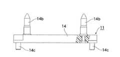
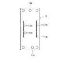
このソケット本体14は、図1及び図3に示すように、長方形状を呈し、中央部に開口部14aが形成されると共に、上面部に一対の位置決めピン14bが設けられ、又、下面部に嵌合ピン14cが突設されている。
【0016】
この位置決めピン14bが、ICパッケージ12を保持するICキャリア20に嵌合されてICソケット11とICキャリア20との位置決めを行うようになっており、そのICキャリア20は、自動機等により搬送されるようになっている。また、嵌合ピン14cは、回路基板13の嵌合孔13aに嵌合されることにより、ICソケット11と回路基板13とが位置決めされるようになっている。
【0017】
このコンタクトピン15は、導電性及びバネ性を有する薄板材料が打抜き加工されて形成され、これらコンタクトピン15は、ICパッケージ12の端子12bの端子数や端子間隔に応じて配設されている。
【0018】
このコンタクトピン15は、図3及び図4に示すように、ソケット本体14に取り付けられるベース部15aを有し、このベース部15aから第1ばね15bが延長されて、この第1ばね15bの先端部側に第1接触部15cが形成され、この第1接触部15cから第2ばね15dが延長されて、この第2ばね15dの先端部側に第2接触部15eが形成されている。
【0019】
そのベース部15aは、ソケット本体14に形成される嵌合孔14dに嵌合されて取り付けられるようになっていると共に、その第1接触部15cは、下方に突出する凸形状を呈し、回路基板13の電極部13bに接触され、第1ばね15bにより、第1接触部15cが回路基板13側に付勢されるようになっている。
【0020】
また、第2接触部15eは、上方に突出する凸形状を呈し、ICパッケージ12の端子12bに接触され、第2ばね15dにより、第2接触部15eが端子12b側に付勢されるようになっている。
【0021】
その第2ばね15dは、第1接触部15cと第2接触部15eとの間に設けられ、ICパッケージ12の端子12bと回路基板13との間の電路となっていると共に、湾曲部15fが一部に形成されている。
【0022】
そして、第2接触部15eが、図1及び図4に示すように、ソケット本体14の開口部14a内に突出している。
【0023】
次に、かかる構成のICソケット11の使用方法について説明する。
【0024】
予め、ICソケット11の嵌合ピン14cを回路基板13の嵌合孔13aに嵌合させて所定の位置に取り付ける。この状態で、コンタクトピン15の第1接触部15cが回路基板13の電極部13bに第1ばね15bの付勢力により圧接されて接圧が確保されている。
【0025】
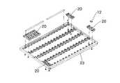
一方、図7に示すように、ハンドラのテストトレー23に、多数のICキャリア20が装着され、このICキャリア20にICパッケージ12が位置決めされて収納され、この状態でテストトレー23が図示省略の装置により搬送されることとなる。そして、そのICキャリア20を、IC試験装置側の回路基板13の所定位置に配置された複数のICソケット11上に位置させる。
【0026】
その後、このテストトレー23を下降させることにより、ICキャリア20に形成された位置決め孔にICソケット11の位置決めピン14bを嵌合させる。
【0027】
この状態で、ICキャリア20ひいてはICパッケージ12と、ICソケット11と、回路基板13とがそれぞれ所定の位置関係で組み付けられる。
【0028】
そして、ハンドラー側の図示省略の圧接子で、ICパッケージ12が上方から押圧されて、ICパッケージ12の端子12bがコンタクトピン15の第2接触部15eに圧接される。
【0029】
この際には、コンタクトピン15の第2ばね15dが弾性変形されて所定の圧接力で、ICパッケージ12の端子12bとコンタクトピン15の第2接触部15eとが当接される。
【0030】
これで、ICパッケージ12がICソケット11を介して回路基板13に電気的に接続されることにより、IC試験装置にてICパッケージ12の試験が行われ、この試験結果に基づいて、良品、不良品の仕分けが行われることとなる。
【0031】
このように第1ばね15bと第2ばね15dとに分割することにより、両ばね15b,15dの動作を小さくすることができるため、各ばね15b,15dの弾性力を大きくできることから、第1接触部15cの回路基板13に対する接圧及び、第2接触部15eのICパッケージ12の端子12bに対する接圧を確保することができる。
【0032】
そして、その第2ばね15dが回路基板13とICパッケージ12の端子12bとの間の電路となることにより、電路を短くできるため、高周波のICパッケージ12の試験を良好に行うことができる。
【0033】
また、第1ばね15bと第2ばね15dの付勢力を変えれば、ICパッケージ12の端子12b又は、回路基板13への接圧を異ならせることができる。
【0039】
なお、上記実施の形態では、「電気部品」として図6に示すようなICパッケージ12を適用したが、これに限らず、他のタイプのICパッケージでも良いし、又、ICパッケージ以外の電気部品でも良い。
【0040】
【発明の効果】
以上説明してきたように、請求項1に記載の発明によれば、ばね部を第1ばねと第2ばねとに分割することにより、両ばねの動作を小さくすることができるため、各ばねの弾性力を大きくできることから、第1接触部の回路基板に対する接圧及び、第2接触部の電気部品に対する接圧を確保することができる。しかも、コンタクトピンは、ソケット本体に取り付けられるベース部を有し、このベース部から第1ばねが延長されて、この第1ばねの先端部側に第1接触部が形成され、この第1接触部から第2ばねが延長されて、この第2ばねの先端部側に第2接触部が形成されたため、一枚の導電性部材からコンタクトピンを簡単に成形することができる。
【0041】
そして、その第2ばねが回路基板と電気部品との間の電路となることにより、電路を短くできるため、高周波の電気部品の試験を良好に行うことができる。
【0042】
請求項2に記載の発明によれば、第1ばねの弾性力と、第2ばねの弾性力とを異ならせることにより、それぞれ任意の接圧に設定することができる。
【図面の簡単な説明】
【図1】この発明の実施の形態1に係るICソケットの平面図である。
【図2】同実施の形態1に係る図1の一部を破断した右側面図である。
【図3】同実施の形態1に係る図1のA−A線に沿う断面図である。
【図4】同実施の形態1に係るコンタクトピン配設状態を示す断面図である。
【図5】同実施の形態1に係る回路基板の平面図である。
【図6】同実施の形態1に係るICパッケージを示す図で、(a)はICパッケージの平面図、(b)は(a)の右側面図である。
【図7】同実施の形態1に係るテストトレー及びICキャリア等の斜視図である。
【図8】従来例を示す断面図である。
【符号の説明】
11 ICソケット(電気部品用ソケット)
12 ICパッケージ(電気部品)
12b 端子
13 回路基板
14 ソケット本体
15 コンタクトピン
15a ベース部
15b第1ばね
15c 第1接触部
15d第2ばね
15e 第2接触部
15f 湾曲部[0001]
BACKGROUND OF THE INVENTION
The present invention relates to an electrical component socket that is interposed between an electrical component such as a semiconductor device (hereinafter referred to as an “IC package”) and a circuit board and electrically connects the electrical component to the circuit board. .
[0002]
[Prior art]
As this type of conventional one, for example, there is the one shown inFIG . The
[0003]
The
[0004]
By being electrically connected in this way, the IC package is tested by the IC test apparatus, and the non-defective product and the defective product are sorted based on the test result.
[0005]
[Problems to be solved by the invention]
However, in such conventional, substantially U-shaped
[0006]
Therefore, the present invention provides a socket for an electrical component that can secure a contact pressure to the circuit board and the electrical component and can shorten the electrical path from the electrical component to the circuit substrate.
[0007]
[Means for Solving the Problems]
In order to achieve the above object, the invention according to claim 1 is directed to a socket body in which an electrical component and a circuit board are disposed on opposite sides, and the electrical component attached to the socket body is connected to the circuit. An electrical component socket having a contact pin for electrical conduction to a substrate, the contact pin having a base portion attached to the socket body, and a first spring extending from the base portion, A first contact portion that is in contact with the circuit board is formed on the distal end side of one spring, a second spring is extended from the first contact portion, and a terminal of the electrical component is disposed on the distal end side of the second spring. A second contact portion is formed, and the first spring biases the first contact portion toward the circuit board, and the second spring attaches the second contact portion toward the terminal side. The first contact portion and the second contact portion. Is provided between the contact portion, with which a path between the terminal and the circuit boardof the electrical component, which curved portion formed in apart, the first contact portion, the circuit board The second spring is pressed against the circuit board by the urging force of the first spring in the state of being disposed in the socket body, and the second contact portion is in the state of being in the state of the electrical component being disposed in the socket body. This is characterized in that the socket foran electric componentis configured such that the elastic member is elastically deformed and is brought into contact with the electric component with a predetermined pressure contact force .
[0008]
According to the second aspect of the present invention, in addition to the configuration of the first aspect, the elastic force of the first spring and the elastic force of the second spring are made different.
[0010]
DETAILED DESCRIPTION OF THE INVENTION
Embodiments of the present invention will be described below.
[0011]
Embodiment 1 of the Invention
1 to 7 show a first embodiment of the present invention.
[0012]
First, the configuration will be described.
[0013]
As shown in FIG. 6, the
[0014]
On the other hand, the
[0015]
As shown in FIGS. 1 and 3, the socket
[0016]
The
[0017]
The
[0018]
As shown in FIGS. 3 and 4, the
[0019]
The
[0020]
Further, the
[0021]
The
[0022]
And the
[0023]
Next, a method of using the
[0024]
The
[0025]
On the other hand, as shown in FIG. 7, a large number of
[0026]
Thereafter, the
[0027]
In this state, the
[0028]
Then, the
[0029]
At this time, the
[0030]
As a result, the
[0031]
By dividing the
[0032]
And since the
[0033]
Further, if the urging force of the
[0039]
In the above embodiment, the
[0040]
【The invention's effect】
As described above, according to the first aspect of the present invention, the movement of both springs can be reduced by dividing the spring portion into the first spring and the second spring. Since the elastic force can be increased, the contact pressure of the first contact portion with respect to the circuit board and the contact pressure of the second contact portion with respect to the electrical component can be ensured.In addition, the contact pin has a base portion that is attached to the socket body, a first spring is extended from the base portion, and a first contact portion is formed on the tip end side of the first spring. Since the second spring is extended from the portion and the second contact portion is formed on the tip end side of the second spring, the contact pin can be easily formed from a single conductive member.
[0041]
And since the 2nd spring becomes an electrical circuit between a circuit board and an electrical component, since an electrical circuit can be shortened, a test of a high frequency electrical component can be performed favorably.
[0042]
According to invention of
[Brief description of the drawings]
FIG. 1 is a plan view of an IC socket according to Embodiment 1 of the present invention.
2 is a right side view in which a part of FIG. 1 according to the first embodiment is cut away. FIG.
3 is a cross-sectional view taken along line AA of FIG. 1 according to the first embodiment. FIG.
4 is a cross-sectional view showing a contact pin arrangement state according to the first embodiment. FIG.
FIG. 5 is a plan view of the circuit board according to the first embodiment.
6A and 6B are diagrams showing the IC package according to the first embodiment, where FIG. 6A is a plan view of the IC package, and FIG. 6B is a right side view of FIG.
7 is a perspective view of a test tray and an IC carrier according to the first embodiment. FIG.
FIG. 8is a cross-sectional view showing a conventional example .
[Explanation of symbols]
11 IC socket (socket for electrical parts)
12 IC package (electrical parts)
14
15f Curved part
Claims (2)
Translated fromJapanese該コンタクトピンは、前記ソケット本体に取り付けられるベース部を有し、該ベース部から第1ばねが延長されて、該第1ばねの先端部側に前記回路基板に接触される第1接触部が形成され、該第1接触部から第2ばねが延長されて、該第2ばねの先端部側に前記電気部品の端子に接触される第2接触部が形成され、
前記第1ばねは、前記第1接触部を前記回路基板側に付勢し、
前記第2ばねは、前記第2接触部を前記端子側に付勢し、前記第1接触部と前記第2接触部との間に設けられて、前記電気部品の端子と前記回路基板との間の電路となっていると共に、湾曲部が一部に形成され、
前記第1接触部は、前記回路基板が前記ソケット本体に配置された状態で、前記第1ばねの付勢力により当該回路基板に圧接され、
前記第2接触部は、前記電気部品が前記ソケット本体に配置された状態で、前記第2ばねが弾性変形して当該電気部品に所定の圧接力で当接されるように構成されたことを特徴とする電気部品用ソケット。A socket for an electrical component having a socket body in which an electrical component and a circuit board are arranged on opposite surfaces, and a contact pin attached to the socket body and electrically conducting the electrical component to the circuit board In
The contact pin has a base portion that is attached to the socket body, and a first contact portion that extends from the base portion and contacts the circuit board is provided on a distal end side of the first spring. Formed, the second spring is extended from the first contact portion, and a second contact portion that is in contact with the terminal of the electrical component is formed on the tip end side of the second spring,
The first spring biases the first contact portion toward the circuit board,
The second spring biases the second contact portion toward the terminal side, and is provided between the first contact portion and the second contact portion, so thatthe terminal of the electrical component and the circuit board And a curved part is formed in part,
The first contact portion is pressed against the circuit board by the biasing force of the first spring in a state where the circuit board is disposed in the socket body.
The second contact portion is configured such that the second spring is elastically deformed and is brought into contact with the electrical component with a predetermined pressing force in a state where the electrical component is disposed on the socket body. A socket for electrical components.
Priority Applications (2)
| Application Number | Priority Date | Filing Date | Title |
|---|---|---|---|
| JP2002050624AJP4053786B2 (en) | 2002-02-27 | 2002-02-27 | Socket for electrical parts |
| US10/372,170US7431591B2 (en) | 2002-02-27 | 2003-02-25 | Socket for electrical parts |
Applications Claiming Priority (1)
| Application Number | Priority Date | Filing Date | Title |
|---|---|---|---|
| JP2002050624AJP4053786B2 (en) | 2002-02-27 | 2002-02-27 | Socket for electrical parts |
Publications (2)
| Publication Number | Publication Date |
|---|---|
| JP2003249323A JP2003249323A (en) | 2003-09-05 |
| JP4053786B2true JP4053786B2 (en) | 2008-02-27 |
Family
ID=27750832
Family Applications (1)
| Application Number | Title | Priority Date | Filing Date |
|---|---|---|---|
| JP2002050624AExpired - Fee RelatedJP4053786B2 (en) | 2002-02-27 | 2002-02-27 | Socket for electrical parts |
Country Status (2)
| Country | Link |
|---|---|
| US (1) | US7431591B2 (en) |
| JP (1) | JP4053786B2 (en) |
Families Citing this family (45)
| Publication number | Priority date | Publication date | Assignee | Title |
|---|---|---|---|---|
| JP4522975B2 (en)* | 2006-06-19 | 2010-08-11 | 東京エレクトロン株式会社 | Probe card |
| JP4750820B2 (en)* | 2008-04-21 | 2011-08-17 | 東京エレクトロン株式会社 | Probe card |
| US9276336B2 (en) | 2009-05-28 | 2016-03-01 | Hsio Technologies, Llc | Metalized pad to electrical contact interface |
| US8955215B2 (en) | 2009-05-28 | 2015-02-17 | Hsio Technologies, Llc | High performance surface mount electrical interconnect |
| WO2011153298A1 (en) | 2010-06-03 | 2011-12-08 | Hsio Technologies, Llc | Electrical connector insulator housing |
| US9536815B2 (en) | 2009-05-28 | 2017-01-03 | Hsio Technologies, Llc | Semiconductor socket with direct selective metalization |
| WO2010147939A1 (en) | 2009-06-17 | 2010-12-23 | Hsio Technologies, Llc | Semiconductor socket |
| WO2010141313A1 (en) | 2009-06-02 | 2010-12-09 | Hsio Technologies, Llc | Compliant printed circuit socket diagnostic tool |
| US8525346B2 (en) | 2009-06-02 | 2013-09-03 | Hsio Technologies, Llc | Compliant conductive nano-particle electrical interconnect |
| US9414500B2 (en) | 2009-06-02 | 2016-08-09 | Hsio Technologies, Llc | Compliant printed flexible circuit |
| US8988093B2 (en) | 2009-06-02 | 2015-03-24 | Hsio Technologies, Llc | Bumped semiconductor wafer or die level electrical interconnect |
| US9231328B2 (en) | 2009-06-02 | 2016-01-05 | Hsio Technologies, Llc | Resilient conductive electrical interconnect |
| WO2011002709A1 (en) | 2009-06-29 | 2011-01-06 | Hsio Technologies, Llc | Compliant printed circuit semiconductor tester interface |
| US9184145B2 (en) | 2009-06-02 | 2015-11-10 | Hsio Technologies, Llc | Semiconductor device package adapter |
| WO2010141298A1 (en) | 2009-06-02 | 2010-12-09 | Hsio Technologies, Llc | Composite polymer-metal electrical contacts |
| US8955216B2 (en) | 2009-06-02 | 2015-02-17 | Hsio Technologies, Llc | Method of making a compliant printed circuit peripheral lead semiconductor package |
| WO2010141318A1 (en)* | 2009-06-02 | 2010-12-09 | Hsio Technologies, Llc | Compliant printed circuit peripheral lead semiconductor test socket |
| WO2010147934A1 (en) | 2009-06-16 | 2010-12-23 | Hsio Technologies, Llc | Semiconductor die terminal |
| US9054097B2 (en) | 2009-06-02 | 2015-06-09 | Hsio Technologies, Llc | Compliant printed circuit area array semiconductor device package |
| US9318862B2 (en) | 2009-06-02 | 2016-04-19 | Hsio Technologies, Llc | Method of making an electronic interconnect |
| US9930775B2 (en) | 2009-06-02 | 2018-03-27 | Hsio Technologies, Llc | Copper pillar full metal via electrical circuit structure |
| US9196980B2 (en) | 2009-06-02 | 2015-11-24 | Hsio Technologies, Llc | High performance surface mount electrical interconnect with external biased normal force loading |
| US9613841B2 (en) | 2009-06-02 | 2017-04-04 | Hsio Technologies, Llc | Area array semiconductor device package interconnect structure with optional package-to-package or flexible circuit to package connection |
| US9603249B2 (en) | 2009-06-02 | 2017-03-21 | Hsio Technologies, Llc | Direct metalization of electrical circuit structures |
| US8987886B2 (en) | 2009-06-02 | 2015-03-24 | Hsio Technologies, Llc | Copper pillar full metal via electrical circuit structure |
| US9136196B2 (en) | 2009-06-02 | 2015-09-15 | Hsio Technologies, Llc | Compliant printed circuit wafer level semiconductor package |
| US8610265B2 (en) | 2009-06-02 | 2013-12-17 | Hsio Technologies, Llc | Compliant core peripheral lead semiconductor test socket |
| US9320133B2 (en) | 2009-06-02 | 2016-04-19 | Hsio Technologies, Llc | Electrical interconnect IC device socket |
| US8912812B2 (en) | 2009-06-02 | 2014-12-16 | Hsio Technologies, Llc | Compliant printed circuit wafer probe diagnostic tool |
| US9699906B2 (en) | 2009-06-02 | 2017-07-04 | Hsio Technologies, Llc | Hybrid printed circuit assembly with low density main core and embedded high density circuit regions |
| US9232654B2 (en) | 2009-06-02 | 2016-01-05 | Hsio Technologies, Llc | High performance electrical circuit structure |
| US9276339B2 (en) | 2009-06-02 | 2016-03-01 | Hsio Technologies, Llc | Electrical interconnect IC device socket |
| WO2010141296A1 (en) | 2009-06-02 | 2010-12-09 | Hsio Technologies, Llc | Compliant printed circuit semiconductor package |
| WO2012074963A1 (en) | 2010-12-01 | 2012-06-07 | Hsio Technologies, Llc | High performance surface mount electrical interconnect |
| WO2010141264A1 (en) | 2009-06-03 | 2010-12-09 | Hsio Technologies, Llc | Compliant wafer level probe assembly |
| WO2010147782A1 (en) | 2009-06-16 | 2010-12-23 | Hsio Technologies, Llc | Simulated wirebond semiconductor package |
| US8984748B2 (en) | 2009-06-29 | 2015-03-24 | Hsio Technologies, Llc | Singulated semiconductor device separable electrical interconnect |
| US8758067B2 (en) | 2010-06-03 | 2014-06-24 | Hsio Technologies, Llc | Selective metalization of electrical connector or socket housing |
| US9350093B2 (en) | 2010-06-03 | 2016-05-24 | Hsio Technologies, Llc | Selective metalization of electrical connector or socket housing |
| US9689897B2 (en) | 2010-06-03 | 2017-06-27 | Hsio Technologies, Llc | Performance enhanced semiconductor socket |
| US10159154B2 (en) | 2010-06-03 | 2018-12-18 | Hsio Technologies, Llc | Fusion bonded liquid crystal polymer circuit structure |
| US9761520B2 (en) | 2012-07-10 | 2017-09-12 | Hsio Technologies, Llc | Method of making an electrical connector having electrodeposited terminals |
| US10506722B2 (en) | 2013-07-11 | 2019-12-10 | Hsio Technologies, Llc | Fusion bonded liquid crystal polymer electrical circuit structure |
| US10667410B2 (en) | 2013-07-11 | 2020-05-26 | Hsio Technologies, Llc | Method of making a fusion bonded circuit structure |
| US9559447B2 (en) | 2015-03-18 | 2017-01-31 | Hsio Technologies, Llc | Mechanical contact retention within an electrical connector |
Family Cites Families (12)
| Publication number | Priority date | Publication date | Assignee | Title |
|---|---|---|---|---|
| US3877064A (en)* | 1974-02-22 | 1975-04-08 | Amp Inc | Device for connecting leadless integrated circuit packages to a printed-circuit board |
| US3993384A (en)* | 1975-05-12 | 1976-11-23 | E. I. Du Pont De Nemours And Company | Connector block |
| US4050755A (en)* | 1976-04-02 | 1977-09-27 | E. I. Du Pont De Nemours And Company | Electrical connector |
| JP2554746B2 (en)* | 1989-07-04 | 1996-11-13 | 山一電機株式会社 | contact |
| FR2703839B1 (en)* | 1993-04-09 | 1995-07-07 | Framatome Connectors France | Intermediate connector between printed circuit board and electronic circuit substrate. |
| JPH10228966A (en)* | 1997-02-12 | 1998-08-25 | Hirose Electric Co Ltd | Intermediate electrical connector |
| JP3687886B2 (en)* | 1998-06-11 | 2005-08-24 | タイコエレクトロニクスアンプ株式会社 | Board mounted connector |
| JP2000133353A (en)* | 1998-10-27 | 2000-05-12 | Hirose Electric Co Ltd | Intermediate electrical connector |
| TW385071U (en)* | 1998-11-24 | 2000-03-11 | Hon Hai Prec Ind Co Ltd | Structure of electrical connector terminals |
| JP3737683B2 (en)* | 1999-09-29 | 2006-01-18 | 日本碍子株式会社 | Contact sheet |
| US6296495B1 (en)* | 1999-11-05 | 2001-10-02 | Hon Hai Precision Ind. Co., Ltd. | Land grid package connector |
| TW515592U (en)* | 2000-01-20 | 2002-12-21 | Hon Hai Prec Ind Co Ltd | Electrical connector |
- 2002
- 2002-02-27JPJP2002050624Apatent/JP4053786B2/ennot_activeExpired - Fee Related
- 2003
- 2003-02-25USUS10/372,170patent/US7431591B2/ennot_activeExpired - Fee Related
Also Published As
| Publication number | Publication date |
|---|---|
| US20030162418A1 (en) | 2003-08-28 |
| JP2003249323A (en) | 2003-09-05 |
| US7431591B2 (en) | 2008-10-07 |
Similar Documents
| Publication | Publication Date | Title |
|---|---|---|
| JP4053786B2 (en) | Socket for electrical parts | |
| JP4133141B2 (en) | Socket for electrical parts | |
| US6471524B1 (en) | IC socket | |
| KR200334763Y1 (en) | System for testing bare ic chips and a socket for such chips | |
| JP2003007412A (en) | Socket for electric component | |
| CN101604000A (en) | Component for testing device of electronic component and testing method of the electronic component | |
| JP2002367746A (en) | Socket and contact for test evaluation of semiconductor package | |
| JPH06112373A (en) | socket | |
| JPH10199646A (en) | Socket for electric part | |
| JP4279039B2 (en) | Socket for electrical parts | |
| JPH09219267A (en) | Bga-ic package testing contact socket | |
| JP3708623B2 (en) | Electrical connection device | |
| JP2002071750A (en) | Carrier and pusher for handler device and handler device | |
| JP2904193B2 (en) | IC socket | |
| JP3725456B2 (en) | Contact pin and IC socket | |
| JP3954161B2 (en) | Socket for electrical parts | |
| JP3670491B2 (en) | Handler socket | |
| JP4303045B2 (en) | Carrier for electrical parts | |
| JP4041341B2 (en) | Socket for electrical parts | |
| JPH11133104A (en) | Socket for testing semiconductor device | |
| JP2000133398A (en) | socket | |
| JP3019355U (en) | Probe card for testing semiconductor wafers | |
| KR100220916B1 (en) | Socket for testing semiconductor chip | |
| JP4651124B2 (en) | IC socket | |
| JP2001143841A (en) | Contact pin group arrangement body, method of manufacturing the same, and socket for electric parts using the same |
Legal Events
| Date | Code | Title | Description |
|---|---|---|---|
| A621 | Written request for application examination | Free format text:JAPANESE INTERMEDIATE CODE: A621 Effective date:20050121 | |
| A977 | Report on retrieval | Free format text:JAPANESE INTERMEDIATE CODE: A971007 Effective date:20070222 | |
| A131 | Notification of reasons for refusal | Free format text:JAPANESE INTERMEDIATE CODE: A131 Effective date:20070306 | |
| A521 | Written amendment | Free format text:JAPANESE INTERMEDIATE CODE: A523 Effective date:20070507 | |
| A131 | Notification of reasons for refusal | Free format text:JAPANESE INTERMEDIATE CODE: A131 Effective date:20070724 | |
| A521 | Written amendment | Free format text:JAPANESE INTERMEDIATE CODE: A523 Effective date:20070925 | |
| TRDD | Decision of grant or rejection written | ||
| A01 | Written decision to grant a patent or to grant a registration (utility model) | Free format text:JAPANESE INTERMEDIATE CODE: A01 Effective date:20071204 | |
| A61 | First payment of annual fees (during grant procedure) | Free format text:JAPANESE INTERMEDIATE CODE: A61 Effective date:20071206 | |
| FPAY | Renewal fee payment (event date is renewal date of database) | Free format text:PAYMENT UNTIL: 20101214 Year of fee payment:3 | |
| R150 | Certificate of patent or registration of utility model | Free format text:JAPANESE INTERMEDIATE CODE: R150 | |
| LAPS | Cancellation because of no payment of annual fees |