JP4050328B2 - High power laser equipment - Google Patents
High power laser equipmentDownload PDFInfo
- Publication number
- JP4050328B2 JP4050328B2JP54581898AJP54581898AJP4050328B2JP 4050328 B2JP4050328 B2JP 4050328B2JP 54581898 AJP54581898 AJP 54581898AJP 54581898 AJP54581898 AJP 54581898AJP 4050328 B2JP4050328 B2JP 4050328B2
- Authority
- JP
- Japan
- Prior art keywords
- volume
- cavity
- laser device
- laser
- gain medium
- Prior art date
- Legal status (The legal status is an assumption and is not a legal conclusion. Google has not performed a legal analysis and makes no representation as to the accuracy of the status listed.)
- Expired - Lifetime
Links
Images


Classifications
- H—ELECTRICITY
- H04—ELECTRIC COMMUNICATION TECHNIQUE
- H04N—PICTORIAL COMMUNICATION, e.g. TELEVISION
- H04N9/00—Details of colour television systems
- H04N9/12—Picture reproducers
- H04N9/31—Projection devices for colour picture display, e.g. using electronic spatial light modulators [ESLM]
- H04N9/3141—Constructional details thereof
- H04N9/315—Modulator illumination systems
- H—ELECTRICITY
- H01—ELECTRIC ELEMENTS
- H01S—DEVICES USING THE PROCESS OF LIGHT AMPLIFICATION BY STIMULATED EMISSION OF RADIATION [LASER] TO AMPLIFY OR GENERATE LIGHT; DEVICES USING STIMULATED EMISSION OF ELECTROMAGNETIC RADIATION IN WAVE RANGES OTHER THAN OPTICAL
- H01S5/00—Semiconductor lasers
- H01S5/04—Processes or apparatus for excitation, e.g. pumping, e.g. by electron beams
- H01S5/042—Electrical excitation ; Circuits therefor
- H01S5/0425—Electrodes, e.g. characterised by the structure
- H01S5/04256—Electrodes, e.g. characterised by the structure characterised by the configuration
- H—ELECTRICITY
- H01—ELECTRIC ELEMENTS
- H01S—DEVICES USING THE PROCESS OF LIGHT AMPLIFICATION BY STIMULATED EMISSION OF RADIATION [LASER] TO AMPLIFY OR GENERATE LIGHT; DEVICES USING STIMULATED EMISSION OF ELECTROMAGNETIC RADIATION IN WAVE RANGES OTHER THAN OPTICAL
- H01S5/00—Semiconductor lasers
- H01S5/10—Construction or shape of the optical resonator, e.g. extended or external cavity, coupled cavities, bent-guide, varying width, thickness or composition of the active region
- H01S5/18—Surface-emitting [SE] lasers, e.g. having both horizontal and vertical cavities
- H01S5/183—Surface-emitting [SE] lasers, e.g. having both horizontal and vertical cavities having only vertical cavities, e.g. vertical cavity surface-emitting lasers [VCSEL]
- H01S5/18308—Surface-emitting [SE] lasers, e.g. having both horizontal and vertical cavities having only vertical cavities, e.g. vertical cavity surface-emitting lasers [VCSEL] having a special structure for lateral current or light confinement
- H—ELECTRICITY
- H01—ELECTRIC ELEMENTS
- H01S—DEVICES USING THE PROCESS OF LIGHT AMPLIFICATION BY STIMULATED EMISSION OF RADIATION [LASER] TO AMPLIFY OR GENERATE LIGHT; DEVICES USING STIMULATED EMISSION OF ELECTROMAGNETIC RADIATION IN WAVE RANGES OTHER THAN OPTICAL
- H01S2301/00—Functional characteristics
- H01S2301/16—Semiconductor lasers with special structural design to influence the modes, e.g. specific multimode
- H01S2301/166—Single transverse or lateral mode
- H—ELECTRICITY
- H01—ELECTRIC ELEMENTS
- H01S—DEVICES USING THE PROCESS OF LIGHT AMPLIFICATION BY STIMULATED EMISSION OF RADIATION [LASER] TO AMPLIFY OR GENERATE LIGHT; DEVICES USING STIMULATED EMISSION OF ELECTROMAGNETIC RADIATION IN WAVE RANGES OTHER THAN OPTICAL
- H01S3/00—Lasers, i.e. devices using stimulated emission of electromagnetic radiation in the infrared, visible or ultraviolet wave range
- H01S3/10—Controlling the intensity, frequency, phase, polarisation or direction of the emitted radiation, e.g. switching, gating, modulating or demodulating
- H01S3/102—Controlling the intensity, frequency, phase, polarisation or direction of the emitted radiation, e.g. switching, gating, modulating or demodulating by controlling the active medium, e.g. by controlling the processes or apparatus for excitation
- H01S3/1022—Controlling the intensity, frequency, phase, polarisation or direction of the emitted radiation, e.g. switching, gating, modulating or demodulating by controlling the active medium, e.g. by controlling the processes or apparatus for excitation by controlling the optical pumping
- H—ELECTRICITY
- H01—ELECTRIC ELEMENTS
- H01S—DEVICES USING THE PROCESS OF LIGHT AMPLIFICATION BY STIMULATED EMISSION OF RADIATION [LASER] TO AMPLIFY OR GENERATE LIGHT; DEVICES USING STIMULATED EMISSION OF ELECTROMAGNETIC RADIATION IN WAVE RANGES OTHER THAN OPTICAL
- H01S3/00—Lasers, i.e. devices using stimulated emission of electromagnetic radiation in the infrared, visible or ultraviolet wave range
- H01S3/10—Controlling the intensity, frequency, phase, polarisation or direction of the emitted radiation, e.g. switching, gating, modulating or demodulating
- H01S3/106—Controlling the intensity, frequency, phase, polarisation or direction of the emitted radiation, e.g. switching, gating, modulating or demodulating by controlling devices placed within the cavity
- H01S3/108—Controlling the intensity, frequency, phase, polarisation or direction of the emitted radiation, e.g. switching, gating, modulating or demodulating by controlling devices placed within the cavity using non-linear optical devices, e.g. exhibiting Brillouin or Raman scattering
- H01S3/109—Frequency multiplication, e.g. harmonic generation
- H—ELECTRICITY
- H01—ELECTRIC ELEMENTS
- H01S—DEVICES USING THE PROCESS OF LIGHT AMPLIFICATION BY STIMULATED EMISSION OF RADIATION [LASER] TO AMPLIFY OR GENERATE LIGHT; DEVICES USING STIMULATED EMISSION OF ELECTROMAGNETIC RADIATION IN WAVE RANGES OTHER THAN OPTICAL
- H01S5/00—Semiconductor lasers
- H01S5/04—Processes or apparatus for excitation, e.g. pumping, e.g. by electron beams
- H01S5/041—Optical pumping
- H—ELECTRICITY
- H01—ELECTRIC ELEMENTS
- H01S—DEVICES USING THE PROCESS OF LIGHT AMPLIFICATION BY STIMULATED EMISSION OF RADIATION [LASER] TO AMPLIFY OR GENERATE LIGHT; DEVICES USING STIMULATED EMISSION OF ELECTROMAGNETIC RADIATION IN WAVE RANGES OTHER THAN OPTICAL
- H01S5/00—Semiconductor lasers
- H01S5/10—Construction or shape of the optical resonator, e.g. extended or external cavity, coupled cavities, bent-guide, varying width, thickness or composition of the active region
- H01S5/14—External cavity lasers
- H01S5/141—External cavity lasers using a wavelength selective device, e.g. a grating or etalon
- H—ELECTRICITY
- H01—ELECTRIC ELEMENTS
- H01S—DEVICES USING THE PROCESS OF LIGHT AMPLIFICATION BY STIMULATED EMISSION OF RADIATION [LASER] TO AMPLIFY OR GENERATE LIGHT; DEVICES USING STIMULATED EMISSION OF ELECTROMAGNETIC RADIATION IN WAVE RANGES OTHER THAN OPTICAL
- H01S5/00—Semiconductor lasers
- H01S5/10—Construction or shape of the optical resonator, e.g. extended or external cavity, coupled cavities, bent-guide, varying width, thickness or composition of the active region
- H01S5/18—Surface-emitting [SE] lasers, e.g. having both horizontal and vertical cavities
- H01S5/183—Surface-emitting [SE] lasers, e.g. having both horizontal and vertical cavities having only vertical cavities, e.g. vertical cavity surface-emitting lasers [VCSEL]
- H01S5/18386—Details of the emission surface for influencing the near- or far-field, e.g. a grating on the surface
- H01S5/18394—Apertures, e.g. defined by the shape of the upper electrode
Landscapes
- Physics & Mathematics (AREA)
- Electromagnetism (AREA)
- Optics & Photonics (AREA)
- Condensed Matter Physics & Semiconductors (AREA)
- General Physics & Mathematics (AREA)
- Engineering & Computer Science (AREA)
- Multimedia (AREA)
- Signal Processing (AREA)
- Nonlinear Science (AREA)
- Plasma & Fusion (AREA)
- Lasers (AREA)
- Semiconductor Lasers (AREA)
- Optical Modulation, Optical Deflection, Nonlinear Optics, Optical Demodulation, Optical Logic Elements (AREA)
Abstract
Description
Translated fromJapanese関連出願
この出願は、1997年3月21に出願された米国仮出願第60/041、185の利益を請求し、その内容をここで参照して取り込む。
発明の背景
今日通常使用されている半導体レーザは、エッジ放射ダイオードレーザと垂直キャビティ(cavity)面放射レーザ(VCSELs)とを有している。エッジ放射レーザにおいて、半導体利得媒体(gain medium)、例えば量子井戸(quantum−well)半導体基板は半導体基板の面上に形成されている。キャビティミラーは、利得媒体を有する共振キャビティを形成するために、基板面に垂直に基板の反対側に形成されるかまたは他の方法で配置される。利得媒体の電気的または光学的供給は、基板の平面に沿った方向へ伝搬するレーザビームを発生する。
エッジ放射レーザは、極めて普通の半導体レーザ装置である。個々の装置として商業的に利用可能で線形バーのアレー(array)は、たとえば、固体レーザを供給するための光学的供給源として使用される。エッジ放射レーザの、代表的には数百ミリワットより大きい適用構造は、通常高順位の空間モード(spatial mode)および複数の周波数において操作する。これは、単一空間モードおよび/または単一周波数において高出力レーザ出力が必要な、それらの応用の使用を阻止する。エッジ放射は、また、非点収差(astigmatism)と、ビームを小さなスポットに焦点を合わせるのを困難にする通常大きなビームの縦横比をかなりの程度有していて、焦点を合わされた出力ビームを必要とする応用に使用できなくする。ビーム品質が悪いエッジ放射レーザは、また、わかりにくく非効率的な非線型光学材料を使用したレーザ出力の周波数重畳(doubling)をする。
従来のVCSELにおいて、キャビティミラーは、半導体基板に成長した半導体利得媒体の向き合った面に形成されるか、または他の方法で配置される。電気的または光学的供給は、基板の面と直交する方向に放射されたレーザビームを発生する。
従来のVCSELsは、光学的通信および光学的連結システムの応用を見出した。VCSELレーザは、約8ミリワット(mW)の連続した波長(continuous wave)(cw)に制限される通常低い基本的空間モードのTEMoo出力によって特徴づけられ、また、数マイクロメータ(μm)のオーダーの小さな基本的モードのビーム直径によってさらに特徴づけられる。ビーム直径が、100μmのオーダーの直径を持った比較的大きな領域のVCSEL放射は、cw出力の数百mWを有する出力ビームを製造できる。しかしながら、従来のVCSELsを高出力の大きい直径で操作すると、通常、高いオーダーの空間モードと複数周波数を有する出力ビームのペナルティをもたらす。垂直外部キャビティ面放射レーザ(VECSEL)としてこの分野で参照される外部キャビティVCSEL構造において、外部リフレクタは外部カプラとして役立つ。外部キャビティVECSEL装置は、VCSEL装置よりも高い基本的空間モード出力を有する。
垂直に発生する半導体レーザの外部キャビティの従来の作業は、低出力の結果となる。たとえば、SanduskyとBrueckの作業は、半導体を励起するために低出力を生成し、光学的供給を使用した。Photonics Technology Letterの1996年第8巻313ページ〜315ページのj.V.SanduskyとS.R.J.Brueckの「cw外部キャビティ面放射レーザ」を参照してほしい。Hadley他の研究において、外部キャビティの電気的に励起されたVCSELは、基本的空間モードにおいて、2.4mWcwと100mW 脈動(pulse)とを生成した。この場合において、120μm迄の放射領域が使用された。Applied Phys. Letterの1993年の第63巻1607ページ〜1609ページのM.A.Hadley、G.C.Wilson、K.Y.Lau、およびJ.S.Smithの「高単一横断モード出力の外部キャビティ面放射レーザダイオード」を参照してほしい。
種々のレーザ応用のために、レーザによって発生されたビームは、周波数変換と周波数重畳(frequency doublihg)が実行される。これは、非線形材料、たとえば、KTP、KTN、KNbO3、LiNbO3をレーザ経路に導入することによって達成される。非線形材料へのビーム投射の周波数は、第2の周波数に変換される。非線形材料は、「重畳結晶」として参照され、材料の性質は、それが結晶を横断するビームの周波数を重畳するのに役立つようなものである。材料による効率的な周波数変換は、通常、高強度で単一モードの投射ビームが必要である。
半導体レーザの周波数重畳は、成功の程度を変えるために、エッジ放射ダイオードレーザキャビティの外部に設けられた重畳結晶を使用して過去において実証されてきた。エッジ放射ダイオードレーザからの出力ビームは、通常、高度に分岐し、効率的な周波数重畳のために理想的に要求されたそれからの光学的フィールド強度と位相前部とを劣化するような、非点収差のある程度と同様な大きな縦横比を有している。光学的フィールド強度を比較的長い経路の長さをある程度越えて維持するために、ダイオードレーザからの光が非線型材料に組み立てられた光学伝搬路に投射される実験が実行されてきた。この技術は、通常複雑で、レーザ光を外部伝搬路に投射するために十分なビーム品質を有している比較的低出力ダイオードレーザを使用する。
過去においていろいろな技術が、十分な変換が可能なようにビームパワーを装備するために試みられた。SPIEのProc.の1980年の第236巻第8ページ〜第18ページのGunter、P.Gunter他による「レーザダイオードを持った光学的周波数重畳用の非線型光学結晶」は、単一経路重畳構造にカリウムニオブ酸塩KNbO3を使用したダイオードレーザ放射の低効率周波数重畳を実証している。他の技術において、Koslovsky他の1987年のOptics Letter12、1014は、周波数変換を達成するために循環パワーを増加する外部リング共振器に単一空間モードのエッジ放射ダイオードレーザとKNbO3を使用している。Koslovsky構造は、非線型結晶の温度を両方の周波数に調波させるのと同様に、リングキャビティのファブリーペロー(fabbry−Perot)共振器に単一周波数レーザの周波数ロックが必要である。これは、周波数ロックを維持するために複雑な結晶配列と波長制御回路とが必要である。
発明の概要
本発明は、上述の制限を克服する単一空間モードにおける高出力レーザ放射を発生するための装置と方法に関する。本発明のレーザは、外部キャビティに形成された場合、効果的周波数変換のために適切な経路長を越えたビームパワー密度を提供するように、出力ビームの周波数変換のために特に受入可能である。
本発明の第1の実施例において、装置は、第1と第2の部分的リフレクタの間に規定された共振キャビティを有している。共振キャビティの構造は、基本的空間または横断するキャビティモードを規定する。利得媒体は、共振キャビティ内に配置され、エネルギー源は、第1の体積(volume)内の利得媒体を付勢する。これが、基本的なキャビティモードを横断する方向で利得媒体に伝搬する自然で誘導エネルギー放射を起こさせる。横断する放射は、次いで、第1の体積の周りに利得媒体の第2の体積を光学的に供給する。自然放射の強さが十分高い場合、逆変換と利得とは、第2の体積で生成される。第1と第2の体積内のエネルギーは、基本的なキャビティモードレーザビーム内に結合される。
基本的なキャビティモードが第1と第2の体積の両方に結合されるように、キャビティの構造を最適化することによって、第2の体積内へ横断的に向けられた第1の体積のエネルギーは、他の方法でも浪費されるが、レーザの全体のパワー効率を改良するために、代わって基本的ビームによって補足される。これを効果的にするために、好ましい実施例において、キャビティミラーは、基本的キャビティモードを第2の体積に断面積に調波させるために選択される。この方法において、基本的空間モードにおけるレーザエネルギーは、利得媒体の第1と第2の両方の体積から効率的に引出される。
好ましい実施例において、第1の体積は実質的に円筒状で断面積の直径がD1であり、第2の体積は実質的に環帯で断面積の外側の直径がD2であって断面積の内側の直径がD1であり、第1と第2の体積は断面積的に実質的に同心である。
利得媒体は、好ましくは、垂直キャビティ構造に半導体材料で形成されている。あるいは、利得媒体は、利得遷移のスペクトル領域に吸収を有する活性化イオンを有した固体材料で形成されてもよい。そのような固体材料の例としてエルビウム(Er):ガラス、イッテルビウム(Yb):ガラス、およびイッテルビウム(Yb):YAGがある。固体材料の場合、供給エネルギーは、好ましくは、たとえばダイオードレーザのような光学的手段によって発生される。
非線型結晶は、レーザ出力周波数を変更するために、光学的キャビティまたはレーザの外へ設けられる。非線型変更用の適切な材料は、KTP、KTN、KNbO3、およびLiNbO3、ならびに、周期的に極化された(poled)LiNbO3のような周期的に極化された材料を有している。
以下に詳細に述べられる本発明の好ましい実施例は、1mmの直径のビーム用として基本的空間モードにおいて100kWを越える内部キャビティ循環パワーレベルを発生することができる。レベルは、非線形材料の基本的放射の調波した変換を生成するために十分である。たとえば、GaInAs利得媒体を使用した半導体構造の周波数重畳は、900nmから1100nmの基本的な波長と、青から緑の波長の周波数重畳出力を提供する。
【図面の簡単な説明】
本発明の上述のおよび他の目的、態様、および利点は、異なった図を通して同様の部品に類似の参照符号を付してある添付した図面に示された、本発明の好ましい実施例の特別な記述から明らかになるであろう。図面は、寸法的には必要ではなく、発明の原理を示すのに代えて強調されている。
図1は、本発明によるVECSELレーザ構造の斜視図。
図2は、本発明による第1の供給された体積から第2の環状の体積への自然で誘導放射の横断する伝搬を示すための図1の構造の切除した側面図。
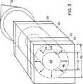
図3は、本発明による第1の供給された体積と第2の環状の体積との関係を示すVCSELレーザ構造の斜視図。
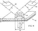
図4は、本発明による光学的増幅装置の構造を示す斜視図。
図5は、出力エネルギーを工学ファイバ内へ結合するための結合構造を示す側面図。
好ましい実施例の詳細な説明
図1は、VECSEL構造における本発明の好ましい実施例の斜視図である。図1のレーザは、半導体基板20を有していて、その第1の面上には、半導体量子井戸利得領域22が形成されている。第1のリフレクタ26、例えばp−Braggリフレクタが、量子井戸領域22上に形成されている。外方の第2のリフレクタ30は、第1のリフレクタ26に向き合って位置している。第1のリフレクタと第2のリフレクタ26、30の間の距離とそれらの各曲率は、共振キャビティ60の基本的なキャビティモードを規定している。第2のリフレクタ30は、図1において、VECSEL構造に従って外部キャビティミラーとして示されている。しかしながら、第2のリフレクタ30は、それに代わって、VCSEL構造を構成するように基板の第2の面に直接隣接する層としても良い。本発明のためにここで使用される用語「リフレクタ」は、部分的におよび/または完全に反射性の材料および/または面を含むことに注目してほしい。第2のリフレクタ30が面した基板20の表面42は、好ましくは、反反射性のコーティング42の処理がされ、境界面を横切る共振キャビティ60のどのようなビームエネルギーも、最小の反射で通過するであろう。好ましい態様は、従来技術において良く知られている。
図2の断面図に示したように、共振キャビティは、電気的な環状のコンタクト28によって電気的に供給され、基板20の向き合った面の環状のコンタクト28と円形のコンタクト40との間で電流38を流すようにする。結果としての合成的な電流の流れ38は、一般に形状が円錐状で、コーンの基部39Aは環状のコンタクト28にあり、コーンの頂部39Bはコンタクト40の近傍にある。頂部39B内の流れは、一般に断面積が環状であって、利得領域22の実質的に円筒状の第1の体積44を付勢するが、第1の体積44は断面積の直径がD1である。直径D1は、好ましくは、利得領域22の厚さよりも実質的に大きい。
直径D1の励起された利得領域22は、キャビティレーザビームの伝搬を横切った方向へ移動する、誘導されたおよび自然放射を矢印48で示されたように生ずる。標準的な従来のVCSELまたはVECSELレーザにおいて、そのようなエネルギーは、装置の外側へ逃げるか、または出力ビーム32に貢献しないエネルギーとして浪費された。本発明の構成においては、この横断エネルギーは、第1の供給された体積を取り巻く環状の第2の体積46に吸収される。この吸収されたエネルギーは、基本的なレーザモード60内への利得、したがってパワーを与える第2の体積46を供給するのに役立つ。
第1の領域D1の電気的または光学的供給が利得を生成すると、この利得は横断方向と長手方向の両方のために生ずる。横断利得長さが長手利得長さよりも大きいので、誘導放射(stimulated emission)をよりその方向に生ずることができる。寸法D1が大きければ大きいほど横断方向への誘導放射用の正味の利得は大きくなる。熱放散と制限が、長手方向における半導体の表面の光学パワー密度による悲劇的な劣化によって設定されるので、より大きい出力はより大きい領域の装置を要する。そのような大きい領域の装置のために、全体のパワー転換効率を減少するような横断する誘導放射の発生によって大きなパワーが失われる。自然放射(spontaneous emission)もまた起きるが、しかし、比較的大きい領域の装置用にはさほど重要ではなくなる。もし隣接する領域が、誘導放射を吸収するために(また、同様に、自然放射が比較的少ないために)構成されていると、別な方法で失われたエネルギーは、第2の領域D2をそれが利得を生ずる程度に光学的に供給するために使用することができる。第2の領域D2内に供給されたエネルギーは、D2に等しいモードくびれ(waist)を利得媒体に生ずるために、外側のミラー30を調整することによって抽出することができる。外側のキャビティミラー30は、D1とD2とによって規定された全体の領域の利得を固定すなわち「クランプ」する。供給された領域の中心から離れた強度の減少と共に、横断する供給の程度が減少するので、第2の領域D2の範囲には限界がある。この限界は、寸法D1と、D1によって規定された領域の供給強度(電気的または光学的)に関連する。
モードくびれ直径D2が与えられと、第2のリフレクタ30用の適切な曲率半径Rと適切な光学キャビティ長さとを有するキャビティを構成するための技術は、この分野で良く知られている。例えば、Herwig KogelnikおよびTingye Leeの、「ビーム、モードおよび共振装置」(1971のCRC発行のCRCレーザハンドブック421〜441頁)を参照してほしい。第2の直径D2は、励起レベルと直径D1との関数である。デザインは、半導体の悲劇的な劣化と第2の直径D2からの熱的パワー放散とによって限定された、循環パワー密度によって限定された最大出力パワーのために最適化されるであろう。キャビティ用のモードくびれ直径は、例えば、キャビティ長さLを第2のリフレクタ30用の固定された曲率半径R用に調整することによって釣り合わすこことができる。
図3は、本発明によるVCSEL構造のレーザの第1の供給体積44と第2の出力体積46との関係を示す斜視図である。供給された第1の体積44は、利得媒体22の領域において直径D1である。矢印48で示された自然および誘導放射の横への伝搬は、第1の体積44を取り巻いている第2の体積46を特徴付ける環状の体積46を光学的に供給するかまたは他の方法で励起する。環状の体積46は、内径D1と外径D2とを有していて、ガウスビーム(Gaussianbeam)分配をする第1の体積44と断面積的に実質的に同心である。基本的なキャビティモードは、第2の体積46の外径にほぼ等しい直径を有することによって最適化され、それによって、第1の体積と第2の体積の両方のエネルギーは捕捉されそしてそれ故出力ビーム32に貢献する。第1の体積44の励起は、電気的または光学的手段によって起こされるであろう。
レーザキャビティパラメータは、好ましくは、最大の操作パワーレベルにおいて、モードくびれを直径D2に実質的に等しく設定するために調節される。単一の平面ミラー26と、図2に示された曲率半径Rを有する単一の凹状の球面ミラー30を有するレーザキャビティにおいて、レーザチップw1と出力ミラーw2とのモードビーム直径は、次によって特徴付けられる:
半導体レーザ装置の好ましい実施例は、多数要素量子井戸構造かまたは、この多数要素量子井戸構造に等しい全体の利得厚さを有する単一利得領域を備えている。十分な単一の通過利得を達成するために、ガリュームインジューム砒素(GaInAs)のような半導体材料の900ナノメータ(nm)から1100nmの波長のレーザ構造は、少なくとも5量子井戸または等しい厚さを有している。より効率的な操作用として、導電性の基板層20のレーザ波長での自由搬送吸収による光学的損出を効率的に克服するために、少なくとも10量子井戸が使用される。単一の量子井戸の代表的な厚さは、ほぼ8nmである。光学的バンドギャップは量子井戸の厚さに依存していて、それ故、利得材料の単一層用の等価厚さは狭い量子井戸用の類似の組成構造から幾分シフトされた波長を有していることに注意してほしい。全体の厚さまたは量子井戸の数は、効率的操作のために全ての内部キャビティの損出を克服するための利得を増加するために増加することができる。これは、そのような構造を均一に成長する能力と、そのような構造用の実際のしきい値電流密度によってのみ限定される。従来のVCSELsは、代表的には、非常に高い反射能力ミラーの間の唯一のまたは幾つかの量子井戸と共に操作する。そのような装置は、低い光学利得を示し、それ故、本発明の装置のように効率的には操作しない。
レーザ装置内に注入された電気の流れまたは光学的供給エネルギーは、良く知られた方法のいずれからでも提供でき、例えば、米国物理学会発行の「半導体レーザ」のG.P.Agarwalの146から157頁がある。本発明の好ましい実施例において、ほとんどの射出電流38は、上述の方程式(1)および(2)によって規定されるような基本的な空間モードの直径D1に等しいかまたはそれよりも小さい直径の環状の領域内に向けられる。
上述のように、エッジ放射ダイオードレーザを使用した低効率周波数重畳は、過去においてGunterおよびKoslovsky他によって実証された。対照的に、本発明の好ましい実施例においては、全体の単一通過利得がエッジ放射ダイオードレーザよりもきわめて低いVCSELまたはVECSEL垂直キャビティレーザ構造を採用している。さらに、本発明の垂直キャビティ装置からの出力は、エッジ放射装置よりもより大きい環状ビーム領域、例えば数百倍も大きい領域に亘って分配する。基本的な循環空間モードにおける達成可能な内部キャビティ循環パワー密度は、半導体表面の悲劇的な劣化のみによって限定されて、数MW/cm2を越えることができる。類似のパワー密度がエッジ放射レーザで達成可能であるのに対して、ビームは、周波数重畳を困難にするダイオードキャビティの導波路に制限される。周波数変換の効率が光学的強度と相互作用領域の長さとの両方に依存するので、ダイオードレーザの周波数重畳は複雑になり、十分な相互作用距離のフィールド強度を維持するための導波路構造をもたらすことができる。ビームが光学的レーザキャビティ内において実質的に拡散しないことにより、高光学フィールド強度が十分に長い相互作用長さを越えて維持できるので、高変換効率が、本発明において達成することができる。高品質のビームは、最近研究された周期的に極化された非線形材料のような、キャビティの外側のあらゆる変換形状のために、より好適な周波数変換状態を提供する。さらに、本発明は、光学的パワーを増加しそれ故非線形変換効率を増加するために、脈打った、利得切り換えされた、および、モードロックされた形状で操作することができる。本発明は、調波周波数変換のみでなく和および差周波数変換にも適用できる。好ましい実施例において、非線形材料は、レーザが単一周波数を操作するファブリーペロー共振を有している。例示的構造が図2に示されていて、基板20と外部ミラー30との間に内部キャビティ非線形結晶58を有している。
上述の各技術の構造、例えば、Sandusky他およびHadley他のような構造は、キャビティ構造を供給された体積のみに釣り合わせることによって限定されるが、本発明はそうではなく、エネルギーを、第1の体積において発生した横断するエネルギー放射によって付勢された第2の体積に加えて、第1の供給された体積から引き出す。
本発明の出力は、上述したように、モード体積の直径を増加することにより、増大することができる。例えば10kWのピークの出力レベルは、直径1ミリメータの利得領域から発生することができる。連続的なcwの出力レベルは、単一要素の装置から10ワットを越え、熱的要件によってのみ限定される。
後ろの方向へ伝搬する第2の調波放射はさらに半導体レーザ構造に吸収されるが、それは、活性化利得領域へ移動する電子と正孔とを生成し、それによって基本的レーザ放射のパワーを増加するするようにしてなされる。これはまた、調波放射の単一終了出力を生成するのと同様に、第2の調波出力の効率増加の効果を有する。他の実施例において、調波放射が利得媒体内に反射して戻らないが中間のミラーによって存在する位置に非線形材料が設けられている3ミラーキャビティが使用できる。リング共振器構造もまた採用できる。
赤外線波長を可視に変換するのに適した代表的な周波数重畳材料は、周期的に極化されたLiNbO3、KTP、およびKNbO3を有する。900nmレンジで操作するGaInAsレーザを使用して、例えば、KTPは1μmの光線を緑の波長に変換するために位相を釣り合わすことができ、KNbO3は赤外光線を青の波長に変換することができる。
この分野で良く知られた内部キャビティ周波数重畳用の多くの構造は、本発明において使用することができる。例えば、パワー密度を増大するために、焦点式レンズをミラー24と30とによって規定されたレーザ共振器内に配置することができる。この技術は、非線形材料または比較的低い非線形性能計数の非線形材料を非常に短い長さで使用することを可能にする。
KTPおよびKNbO3のような重畳材料のために、本発明の構造において可能な循環パワーレベル用の活性結晶長さは1cmよりもかなり短い。比較的短い非線形材料の長さは、条件に釣り合う比較的広範囲な温度と波長位相を提供することができる。例えば、KNbO3用として、1mmまたはそれ以下の結晶長さは、セ氏数度以上の温度位相釣り合いバンド幅、および数ナノメータの波長バンド幅が提供できる。そのような広い受容レンジは、そのような装置の製造と操作をかなり実用的にする。波長は、利得媒体材料の合金組成の選択によって制御されるであろうが、正確な波長制御は、内部キャビティエタロン(etalon)またはこの分野で良く知られた他の波長制御技術によって達成可能である。KTPを含む他の非線形材料にも同様の結果が適用する。
半導体の利得領域22は好ましくは、マルチ要素量子井戸構造を有している。あるいは、全体の利得厚さがマルチ量子井戸構造のそれと等しい単一の利得領域を採用しても良い。十分な単一の通過利得を達成するために、GaInAsで作られた代表的には900nmから1100nm波長レーザ構造用の多くの量子井戸は、5以上で、代表的には10と25井戸の間の範囲である。電気的または光学的励起の何れかを使用する脈動条件下で操作する高ピークパワー装置用として、井戸の数は、50以上となろう。限界は、多くの応力のない量子井戸層を成長させるための実用的な能力によって管理される。この場合において、ヘテロ構造は、より効果的な選択であろう。高ピークパワー装置は、例えば、供給源としての高出力Q切り換え固体レーザを使用することによって作ることができる。
従来の垂直キャビティ半導体レーザは、代表的には、唯一または幾つかの量子井戸と非常な高反射性キャビティミラーと共に操作する。そのような装置は、本来の低光学利得により、本発明における効率のように操作しないであろう。実質利得は、基板材料22の自由搬送損出と、非線形材料と内部キャビティ光学要素の関連された反反射コーティングにおける光学損出とを含む外側キャビティにおける損出を克服するのに十分である。
図2は、半導体基板20に形成された代表的な量子井戸装置22を示している。高度に反射性のミラー26が、レーザ共振器の1つのミラーを提供するために装置の背面に増加される。頂部クラッド層は、非反射被覆42ができレーザ波長の光学吸収が低い導電性の接点として役立つ。他の実施例において、第2の調波放射よりも大きい光学的バンドギャップを持った電気的に導電性の材料は、キャリアの拡散長さよりも小さい厚さで、基本的レーザ放射に透過し、そして活動的な材料と熱くて幅のあるバンドギャップ材料との間で成長した第2の調波放射の吸収する第2の層を持った導電層として役立ち、利得領域内に拡散するために光学的に付勢されたキャリアを可能にする。厚い導電性の材料は、例えば、蒸着されたスズ酸化物を有する。単一周波数操作は、例えば、エタロンをキャビティに導くことによって達成される。あるいは、非線形結晶58が同様に周波数選択要素として役立っても良い。
高出力で可視波長を発生する能力は、プロジェクションディスプレー、読み出しおよび書き込みの光学的ディスク、光学的ホログラフィック記憶装置、およびバイオ蛍光センサを含む出願の範囲で本発明を魅力的にする。プロジェクションディスプレーの場合用に、色の3原則が発生できる。例えば、青の波長と緑の波長は、GaInAs半導体レーザの出力を波長重畳することによって生成でき、この出力は、900nm〜1100nm以上の範囲の波長から選択される。適切な波長重畳材料は、緑の波長用のKTPと、青の波長のKNbO3を含んでいる。パワーはそのような装置を使用しているアレー(array)で測定される。数十ワットの出力パワーレベルが発生する。そのようなアレーからの出力はアレーの要素間のコヒーレンスがないので、スペックル(speckle)の効果は、ディスプレーシステムにおいて投影された像の品質に影響を与えないように大きく減少する。アレー装置の場合において、出力カプラは、リソグラフィ的に製造された2光学系ミラーまたはマイクロミラーのアレーを有していて、その位置は、ダイオードレーザ発生領域の中心に正確に整列される。
本発明に採用した投影ディスプレーシステムは、液晶空間光変調装置のような種々の電球装置、Texas Instruments社から販売されているようなマイクロミラー、および、カリフォルニア州サニーヴェールのSilicon Light Machine社で開発されたようなグレーチィング(grating)偏向電球を使用して操作できる。レーザ源のアレーのために、電球の全ての要素は、各レーザビームが拡がり離れた区域で重なることができるように、あらゆるレーザ源によって照射することができる。このようにして、ある要素がなくともシステムの操作を大きく落とすことはない。2光学系レンズが、全ての利用可能なレーザ放射を効果的に使用するために、電球の各画素にシルクハット(top−hat)供給レーザ光を収束するのに使用できる。
本発明は、その好ましい実施例に関して特に示され述べられてきたが、当業者にとって、形式や詳細の種々の変更は、添付した請求項によって規定された発明の精神と範疇から離れることなくすることができる。
他の実施例として、図4は、光学的増幅器70として構成された本発明の斜視図である。レーザ構成において、光学的増幅器70の構成は、半導体基板20、半導体利得媒体22、および第1のリフレクタ26を有している。光学的増幅器70が共振キャビティを有していないので、第2のリフレクタは必要がないことに注目してほしい。利得媒体22の第1の体積44は、電気的または光学的エネルギー56と共に供給される。第1の体積44は、通常、直径D1を有する断面的に円形である。上述したように、これは、第1の体積44の周りで第2の体積46内への横断したエネルギーの誘導的で同時的な伝搬を起こす。好ましい実施例において、第2の体積46は、断面積が実質的に円形で、その直径はD2である。直径D2の入射ビーム50と第1の振幅は、供給された領域で、第1の体積44と第2の体積46との両方によって重ね合わされ付勢されるようになされる。入射ビーム50は、ミラー26で反射し、そして、同様の直径D2の出力ビーム52として解放される。出力ビーム52は、付勢された利得領域46で増幅され、そしてそれ故、入射ビーム50よりも高い強度である。そのような複数の利得要素が、システムの全体の利得を増加するために使用される。
第2の他の実施例が図5に示されていて、光学結合の側面が示されている。単一のミラー/レンズ要素70は、VECSELレーザ78用の共振装置ミラーとして操作する第1の凹面72と、光学ファイバ76内にレーザ放射32を向けるための収束要素として操作する第2の凸面74とを有している。光学ファイバ76は、単一モードまたはマルチモードのファイバで構成されていても良く、レーザエネルギーがファイバの沢山の開口内に実質的に向けられるように、レーザ放射32の焦点に位置している。第1の面72の反射性は、レーザ装置78からの出力が最大になるように最適化されるが、第2の面74と光学ファイバ76の入射面75とは、反射性を最小化するのにレーザ波長で反反射性の被覆がされている。
組み立て中において、ミラー/レンズ要素70は、レーザ出力結合を最大化するために整列され配置されていて、はんだ付け、エポキシおよび/またはレーザ溶接のような、良く知られた技術で固定される。ファイバは、次いで収束された放射32を受けるために位置付けられ、上述した技術の何れかによって設定される。この実施例は、キャビティミラーの機能と協同することによりファイバにエネルギーを収束するのに必要な光学要素の数の減少と、出力レンズを単一要素内へ入れることを提供する。Related applications
This application claims the benefit of US Provisional Application No. 60 / 041,185, filed Mar. 21, 1997, the contents of which are hereby incorporated by reference.
Background of the Invention
Semiconductor lasers commonly used today include edge emitting diode lasers and vertical cavity surface emitting lasers (VCSELs). In an edge emitting laser, a semiconductor gain medium, for example a quantum well semiconductor substrate, is formed on the surface of the semiconductor substrate. The cavity mirror is formed or otherwise disposed on the opposite side of the substrate perpendicular to the substrate surface to form a resonant cavity with a gain medium. The electrical or optical supply of the gain medium generates a laser beam that propagates in a direction along the plane of the substrate.
Edge emitting lasers are very common semiconductor laser devices. Commercially available as individual devices, linear bar arrays are used, for example, as an optical source for supplying solid state lasers. Application structures of edge emitting lasers, typically larger than a few hundred milliwatts, typically operate in higher order spatial modes and multiple frequencies. This prevents the use of those applications where high power laser power is required in a single spatial mode and / or a single frequency. Edge radiation also has a significant output beam astigmatism and usually a large beam aspect ratio that makes it difficult to focus the beam on a small spot and requires a focused output beam It cannot be used for applications. Edge-emitting lasers with poor beam quality also do frequency doubling of the laser output using non-obvious and inefficient nonlinear optical materials.
In conventional VCSELs, the cavity mirrors are formed on opposite surfaces of a semiconductor gain medium grown on a semiconductor substrate, or otherwise disposed. The electrical or optical supply generates a laser beam emitted in a direction perpendicular to the plane of the substrate.
Conventional VCSELs have found applications in optical communication and optical coupling systems. VCSEL lasers are typically low fundamental spatial mode TEM limited to a continuous wave (cw) of about 8 milliwatts (mW).oo Characterized by the power and further characterized by a small fundamental mode beam diameter on the order of a few micrometers (μm). A relatively large area of VCSEL radiation with a beam diameter on the order of 100 μm can produce an output beam with a cw output of several hundred mW. However, operating conventional VCSELs with large diameters of high power typically results in high order spatial modes and output beam penalties with multiple frequencies. In an external cavity VCSEL structure referred to in the art as a vertical external cavity surface emitting laser (VECSEL), the external reflector serves as an external coupler. The external cavity VECSEL device has a higher fundamental spatial mode output than the VCSEL device.
The conventional operation of the external cavity of a vertically generated semiconductor laser results in low power. For example, the work of Sandusky and Brueck produced low power and used an optical supply to excite the semiconductor. Photonics Technology Letter 1996, Vol. 8, pp. 313-315. V. Sandusky and S.M. R. J. et al. See Brueck's "cw external cavity surface emitting laser". In a study by Hadley et al., An electrically excited VCSEL in the external cavity produced 2.4 mWcw and 100 mW pulsations in the fundamental spatial mode. In this case, a radiation area up to 120 μm was used. Applied Phys. Letter 1993, Volume 63, pages 1607 to 1609. A. Hadley, G.M. C. Wilson, K.M. Y. Lau, and J.A. S. See Smith's "External cavity surface emitting laser diode with high single transverse mode output".
For various laser applications, the laser-generated beam is subjected to frequency conversion and frequency doublehg. This is a non-linear material such as KTP, KTN, KNbOThree LiNbOThree Can be achieved by introducing a laser into the laser path. The frequency of beam projection onto the non-linear material is converted to a second frequency. Non-linear materials are referred to as “superimposed crystals” and the nature of the material is such that it helps to superimpose the frequency of the beam traversing the crystal. Efficient frequency conversion by material usually requires a high intensity, single mode projection beam.
Semiconductor laser frequency superposition has been demonstrated in the past using superposition crystals placed outside the edge-emitting diode laser cavity to vary the degree of success. The output beam from an edge-emitting diode laser is typically highly divergent and is astigmatism that degrades the optical field strength and phase front from it ideally required for efficient frequency superposition. It has a large aspect ratio similar to the degree of aberration. In order to maintain the optical field intensity beyond some length of the relatively long path, experiments have been performed in which light from a diode laser is projected onto an optical propagation path assembled in a non-linear material. This technique typically uses a relatively low power diode laser that is complex and has sufficient beam quality to project laser light onto an external propagation path.
In the past, various techniques have been tried to equip the beam power so that sufficient conversion is possible. SPIE Proc. 1980, Vol. 236, pages 8-18, Gunter, P. et al. Gunter et al., “Nonlinear Optical Crystals with Laser Diodes for Optical Frequency Superimposition,” have potassium niobate KNbO in a single-path superposition structure.Three Demonstrates low-efficiency frequency superposition of diode laser radiation using In another technology, Koslovsky et al., 1987 Optics Letter 12, 1014, uses a single spatial mode edge emitting diode laser and KNbO in an external ring resonator that increases the circulating power to achieve frequency conversion.Three Is used. The Koslovsky structure requires a single-frequency laser frequency lock in the Fabry-Perot cavity of the ring cavity, as well as to tune the temperature of the nonlinear crystal to both frequencies. This requires a complex crystal arrangement and wavelength control circuit to maintain frequency lock.
Summary of the Invention
The present invention relates to an apparatus and method for generating high power laser radiation in a single spatial mode that overcomes the above limitations. The laser of the present invention is particularly acceptable for frequency conversion of the output beam so as to provide a beam power density beyond the appropriate path length for effective frequency conversion when formed in an external cavity. .
In a first embodiment of the invention, the apparatus has a resonant cavity defined between the first and second partial reflectors. The structure of the resonant cavity defines the fundamental space or transverse cavity mode. A gain medium is disposed in the resonant cavity, and an energy source energizes the gain medium in the first volume. This causes natural induced energy radiation that propagates to the gain medium in a direction that traverses the fundamental cavity mode. The transverse radiation then optically supplies a second volume of gain medium around the first volume. If the intensity of natural radiation is high enough, the inverse transform and gain are generated in the second volume. The energy in the first and second volumes is coupled into the basic cavity mode laser beam.
By optimizing the structure of the cavity such that the fundamental cavity mode is coupled to both the first and second volumes, the energy of the first volume directed transversely into the second volume Is wasted in other ways, but is instead supplemented by a basic beam to improve the overall power efficiency of the laser. To make this effective, in the preferred embodiment, a cavity mirror is selected to tune the fundamental cavity mode to a second volume in cross-sectional area. In this way, laser energy in the fundamental spatial mode is efficiently extracted from both the first and second volumes of the gain medium.
In a preferred embodiment, the first volume is substantially cylindrical and has a cross-sectional diameter of D1 And the second volume is substantially an annulus and the outer diameter of the cross-sectional area is D2 And the inner diameter of the cross-sectional area is D1 And the first and second volumes are substantially concentric in cross-sectional area.
The gain medium is preferably formed of a semiconductor material in a vertical cavity structure. Alternatively, the gain medium may be formed of a solid material with activated ions having absorption in the spectral region of the gain transition. Examples of such solid materials are erbium (Er): glass, ytterbium (Yb): glass, and ytterbium (Yb): YAG. In the case of solid materials, the supply energy is preferably generated by optical means such as a diode laser.
Non-linear crystals are placed out of the optical cavity or laser to change the laser output frequency. Suitable materials for non-linear modification are KTP, KTN, KNbOThree And LiNbOThree As well as periodically poled LiNbOThree And periodically poled material.
The preferred embodiment of the present invention, described in detail below, can generate internal cavity circulation power levels in excess of 100 kW in the fundamental spatial mode for a 1 mm diameter beam. The level is sufficient to produce a harmonic transformation of the fundamental radiation of the nonlinear material. For example, frequency superposition of a semiconductor structure using a GaInAs gain medium provides a frequency superposition output of fundamental wavelengths from 900 nm to 1100 nm and blue to green wavelengths.
[Brief description of the drawings]
The foregoing and other objects, aspects, and advantages of the present invention will be apparent from the following detailed description of the preferred embodiment of the present invention, as illustrated in the accompanying drawings in which like reference numerals refer to like parts throughout the different views. It will be clear from the description. The drawings are not necessarily to scale, emphasis instead being placed on illustrating the principles of the invention.
FIG. 1 is a perspective view of a VECSEL laser structure according to the present invention.
FIG. 2 is a cutaway side view of the structure of FIG. 1 to show the transverse propagation of natural stimulated radiation from a first supplied volume to a second annular volume according to the present invention.
FIG. 3 is a perspective view of a VCSEL laser structure showing the relationship between a first supplied volume and a second annular volume according to the present invention.
FIG. 4 is a perspective view showing the structure of the optical amplifying device according to the present invention.
FIG. 5 is a side view showing a coupling structure for coupling output energy into an engineering fiber.
Detailed Description of the Preferred Embodiment
FIG. 1 is a perspective view of a preferred embodiment of the present invention in a VECSEL structure. The laser shown in FIG. 1 has a
As shown in the cross-sectional view of FIG. 2, the resonant cavity is electrically supplied by an electrical
Diameter D1 The
First region D1 When the electrical or optical supply of the current produces a gain, this gain occurs for both the transverse and longitudinal directions. Since the transverse gain length is greater than the longitudinal gain length, stimulated emission can be generated in that direction more. Dimension D1 The larger the is, the greater the net gain for stimulated emission in the transverse direction. Since heat dissipation and limitations are set by catastrophic degradation due to the optical power density of the semiconductor surface in the longitudinal direction, higher power requires a larger area of equipment. For such large area devices, significant power is lost due to the generation of transverse induced radiation that reduces the overall power conversion efficiency. Spontaneous emission also occurs, but is less important for relatively large area devices. If the adjacent region is configured to absorb stimulated radiation (and also because of the relatively low spontaneous radiation), the energy lost otherwise is the second region D.2 Can be used optically to the extent that it produces gain. Second region D2 The energy supplied inside is D2 Can be extracted by adjusting the
Mode constriction diameter D2 Are well known in the art for constructing cavities having a suitable radius of curvature R and a suitable optical cavity length for the
FIG. 3 is a perspective view showing the relationship between the
The laser cavity parameter preferably has a mode constriction diameter D at the maximum operating power level.2 Adjusted to set substantially equal to. In a laser cavity having a
The preferred embodiment of the semiconductor laser device comprises a multi-element quantum well structure or a single gain region having an overall gain thickness equal to the multi-element quantum well structure. To achieve a sufficient single pass gain, a 900 nanometer (nm) to 1100 nm wavelength laser structure of a semiconductor material such as gallium indium arsenide (GaInAs) has at least 5 quantum wells or equal thickness. is doing. For more efficient operation, at least 10 quantum wells are used to efficiently overcome the optical loss due to free carrier absorption at the laser wavelength of the
The electrical flow or optical supply energy injected into the laser device can be provided by any of the well-known methods, such as G.S. P. There are pages 146 to 157 of Agarwal. In the preferred embodiment of the present invention, most of the emission current 38 is the fundamental spatial mode diameter D as defined by equations (1) and (2) above.1 In an annular region with a diameter equal to or smaller than.
As mentioned above, low efficiency frequency superposition using edge emitting diode lasers has been demonstrated in the past by Gunter and Koslovsky et al. In contrast, the preferred embodiment of the present invention employs a VCSEL or VECSEL vertical cavity laser structure where the overall single pass gain is much lower than edge emitting diode lasers. Furthermore, the output from the vertical cavity device of the present invention is distributed over a larger annular beam area, eg, several hundred times larger than the edge emitter. The achievable internal cavity circulation power density in the basic circulation space mode is limited only by the catastrophic degradation of the semiconductor surface and is several MW / cm2 Can be exceeded. While similar power densities can be achieved with edge-emitting lasers, the beam is limited to diode cavity waveguides that make frequency superposition difficult. Since the efficiency of frequency conversion depends on both the optical intensity and the length of the interaction region, the frequency superposition of the diode laser is complicated, resulting in a waveguide structure to maintain a sufficient interaction distance field strength be able to. High conversion efficiency can be achieved in the present invention because the high optical field intensity can be maintained beyond a sufficiently long interaction length by not substantially diffusing the beam in the optical laser cavity. A high quality beam provides a more favorable frequency conversion state for any conversion shape outside the cavity, such as the recently studied periodically poled nonlinear material. Furthermore, the present invention can be operated in a pulsed, gain-switched and mode-locked configuration to increase optical power and therefore increase non-linear conversion efficiency. The present invention can be applied not only to harmonic frequency conversion but also to sum and difference frequency conversion. In the preferred embodiment, the nonlinear material has a Fabry-Perot resonance where the laser operates at a single frequency. An exemplary structure is shown in FIG. 2 having an internal cavity
While the structures of each of the above-mentioned techniques, such as Sandusky et al. And Hadley et al., Are limited by balancing the cavity structure only to the supplied volume, the present invention does not, but the energy In addition to the second volume energized by the transverse energy radiation generated in the first volume, it is withdrawn from the first delivered volume.
The output of the present invention can be increased by increasing the diameter of the mode volume, as described above. For example, a peak power level of 10 kW can be generated from a gain region of 1 millimeter diameter. The continuous cw power level exceeds 10 watts from a single element device and is limited only by thermal requirements.
The second harmonic radiation propagating in the backward direction is further absorbed by the semiconductor laser structure, which generates electrons and holes that move to the activation gain region, thereby reducing the power of the fundamental laser radiation. It is made to increase. This also has the effect of increasing the efficiency of the second harmonic output, as well as producing a single-ended output of harmonic radiation. In other embodiments, a three-mirror cavity can be used in which the harmonic radiation does not reflect back into the gain medium but is provided with a non-linear material at a location that is present by an intermediate mirror. A ring resonator structure can also be employed.
A typical frequency superposition material suitable for converting infrared wavelengths to visible is a periodically poled LiNbO.Three , KTP, and KNbOThree Have Using a GaInAs laser operating in the 900 nm range, for example, KTP can balance phase to convert 1 μm rays to green wavelengths, and KNbOThree Can convert infrared rays into blue wavelengths.
Many structures for internal cavity frequency superposition well known in the art can be used in the present invention. For example, a focusing lens can be placed in a laser resonator defined by
KTP and KNbOThree For superposition materials such as, the active crystal length for circulating power levels possible in the structure of the present invention is much shorter than 1 cm. The relatively short non-linear material length can provide a relatively wide range of temperatures and wavelength phases commensurate with conditions. For example, KNbOThree For use, a crystal length of 1 mm or less can provide a temperature phase balance bandwidth of several degrees Celsius and a wavelength bandwidth of a few nanometers. Such a wide acceptance range makes the manufacture and operation of such devices quite practical. The wavelength will be controlled by the choice of the alloy composition of the gain medium material, but precise wavelength control can be achieved by an internal cavity etalon or other wavelength control techniques well known in the art. . Similar results apply to other nonlinear materials including KTP.
The
Conventional vertical cavity semiconductor lasers typically operate with only one or several quantum wells and a very highly reflective cavity mirror. Such a device will not operate like the efficiency in the present invention due to its inherently low optical gain. The substantial gain is sufficient to overcome the loss in the outer cavity including the free transport loss of the
FIG. 2 shows a representative
The ability to generate visible wavelengths at high powers makes the present invention attractive within the scope of applications that include projection displays, read and write optical discs, optical holographic storage devices, and biofluorescent sensors. Three principles of color can be generated for the projection display case. For example, the blue wavelength and the green wavelength can be generated by wavelength superimposing the output of the GaInAs semiconductor laser, and the output is selected from wavelengths in the range of 900 nm to 1100 nm or more. Suitable wavelength superposition materials are KTP for green wavelengths and KNbO for blue wavelengths.Three Is included. Power is measured in an array using such a device. An output power level of several tens of watts is generated. Since the output from such an array has no coherence between the elements of the array, the effect of speckle is greatly reduced so as not to affect the quality of the image projected in the display system. In the case of an array device, the output coupler has a lithographically manufactured two-optical mirror or micromirror array whose position is precisely aligned to the center of the diode laser generation region.
The projection display system employed in the present invention was developed by various light bulb devices such as liquid crystal spatial light modulators, micromirrors such as those sold by Texas Instruments, and Silicon Light Machine, Sunnyvale, California. It can be operated using a grating deflecting bulb. Due to the array of laser sources, all elements of the bulb can be illuminated by any laser source so that each laser beam can overlap in a distant area. In this way, the operation of the system is not greatly reduced even if there is no element. Two optics lenses can be used to focus the top-hat supply laser light on each pixel of the bulb in order to effectively use all available laser radiation.
Although the invention has been particularly shown and described with respect to preferred embodiments thereof, it will be apparent to those skilled in the art that various changes in form and detail do not depart from the spirit and scope of the invention as defined by the appended claims. Can do.
As another example, FIG. 4 is a perspective view of the present invention configured as an
A second alternative embodiment is shown in FIG. 5, where the side of the optical coupling is shown. A single mirror /
During assembly, the mirror /
Claims (25)
Translated fromJapanese予め定められたキャビティ構造を有する共振キャビティ(60)を規定する第1と第2のリフレクタ(26)、(30)と;
予め定められた厚さを有し前記共振キャビティ内に配置された利得媒体(22)と;および
電流(38)が前記利得媒体(22)の第1の体積(44)内に制限されて前記利得媒体(22)を通って流れるようにするためのエネルギー源と有していて;
前記予め定められたキャビティ構造は、
前記第1の体積(44)に対応する横断する寸法(D1)よりも大きい予め定められたモードくびれ寸法(D2)に関連するレーザビーム(32)の基本的なキャビティモードを規定し、前記横断する寸法は、利得媒体(22)の前記厚さより大きく、および
w12=4λL/π[(R−L)/L]1/2(1)
W22=4λL/π[L/(R−L)]1/2(2)
の第(1)式と第(2)式で規定されるキャビティ構造であって、w1は第1のリフレクタ(26)上のモードのレーザビーム直径、w2は第2のリフレクタ(30)上のモードのレーザビーム直径、Lは前記第1のリフレクタ(26)と前記第2のリフレクタ(30)との間の距離であるキャビティ長さ、λはレーザビームの波長、Rは前記第2のリフレクタ(30)の曲率半径であり;
前記利得媒体(22)の第1の体積(44)内に制限されて流された前記電流(38)は、前記第1の体積(44)から前記基本的なキャビティモードを横断する方向へ前記利得媒体(22)内で伝搬するための自然放射光による光学的エネルギー放射(48)を生じさせ;
横断する光学的エネルギー放射(48)は、前記第1の体積(44)の周りに前記利得媒体(22)の第2の体積(46)を光学的に励起し;
前記予め定められたモードくびれ寸法(D2)は、前記横断する光学的エネルギー放射(48)の予め定められた最大レベルで前記第2の体積(46)の対応する横断する寸法に一致し;
前記第1と第2の体積(44)、(46)内のエネルギーは、前記予め定められたキャビティ構造によって前記基本的なキャビティモード内に結合されているレーザ装置。A vertical cavity surface emitting laser device comprising:
First and second reflectors (26), (30) defining a resonant cavity (60) having a predetermined cavity structure;
Predetermined thickness is disposed in the resonant cavity has a gain medium (22); and a current (38) isrestricted to the first volume (44) of said gain medium (22) An energy source for flowing through the gain medium (22);
The predetermined cavity structure is:
Defining a fundamental cavity mode of the laser beam (32) associated with a predetermined mode constriction dimension (D2) greater than a transverse dimension (D1) corresponding to the first volume (44); dimensions, the I thicknessRedirecting a listening of the gain medium (22), and that
w12= 4λL / π [(R−L) / L]1/2(1)
W22= 4λL / π [L / (RL)]1/2(2)
The cavity structure defined by the first and second formulas (1) and (2), where w1is the laser beam diameter of the mode on the first reflector (26), and w2is the second reflector (30). The upper mode laser beam diameter, L is the cavity length which is the distance between the first reflector (26) and the second reflector (30), λ is the wavelength of the laser beam, and R is the second The radius of curvature of the reflector (30) of the
First volume (44) is limited in it streamed said currentof said gain medium (22) (38), the direction ofthe transverse cross-sectionalsaid basic cavity modefrom said first volume (44)Producing optical energy radiation (48)by natural radiation to propagate in the gain medium (22);
Transverse optical energy radiation (48) opticallyexcites a second volume (46) of the gain medium (22) around the first volume (44);
Said predetermined mode waist dimension (D2) ismatch the corresponding transverse dimension of said second volume at a maximum level predetermined optical energy radiation (48) (46) to said transverse;
Laser apparatus wherein energy in the first and second volumes (44), (46) is coupled into the basic cavity mode by the predetermined cavity structure.
第1と第2のリフレクタ(26)、(30)を配置し、それによってレーザ装置の基本的な放射モード(60)を規定するステップを有し;
前記規定するステップは、
w12=4λL/π[(R−L)/L]1/2(1)
W22=4λL/π[L/(R−L)]1/2(2)
の第(1)式と第(2)式で規定されるキャビティ構造を形成するものであって、w1は第1のリフレクタ(26)上のモードのレーザビーム直径、w2は第2のリフレクタ(30)上のモードのレーザビーム直径、Lは前記第1のリフレクタ(26)と前記第2のリフレクタ(30)との間の距離であるキャビティ長さ、λはレーザビームの波長、Rは前記第2のリフレクタ(30)の曲率半径であり;
第1のコンタクト(40)を前記第1のリフレクタ(26)に配置し、それによってレーザ装置の作動領域(22)に第1の体積(44)を規定するステップを有し、前記第1の体積(44)は、作動領域(22)の厚さよりも大きい横断する寸法(D1)を備えていて;
第1の体積に制限され、それによって第1の体積(44)内に光学的エネルギー放射を生成するように第1のコンタクト(40)を介して電流を印加するステップを有し;
横断する自然放射光による光学的放射(48)を作動領域に沿って第1の体積(44)からこの第1の体積(44)に直接隣接する第2の体積(46)に伝搬し、それによって前記第2の体積(46)を光学的に誘導するステップと;および、
第1と第2の体積(44)、(46)の両方の光学的エネルギー放射を結合するために、第1と第2のリフレクタ(26)、(30)を基本的な放射モード内に適合するステップを有し、予め定められたモードくびれ寸法(D2)は、前記第1の体積(44)の前記横断する寸法(D1)よりも大きく、前記横断する光学的エネルギー放射(48)の予め定められた最大レベルで前記第2の体積(46)の対応した横断する寸法に一致している方法。A method for improving the efficiency of a laser device comprising:
Disposing first and second reflectors (26), (30), thereby defining a basic radiation mode (60) of the laser device;
The defining step includes:
w12= 4λL / π [(R−L) / L]1/2(1)
W22= 4λL / π [L / (RL)]1/2(2)
In which the cavity structure defined by the equations (1) and (2) is formed, w1is the laser beam diameter of the mode on the first reflector (26), and w2is the second The laser beam diameter of the mode on the reflector (30), L is the cavity length which is the distance between the first reflector (26) and the second reflector (30), λ is the wavelength of the laser beam, R Is the radius of curvature of the second reflector (30);
Disposing a first contact (40) in the first reflector (26), thereby defining a first volume (44) in an operating region (22) of the laser device, the first contact (40)comprising : volume (44),than the thickness of the working region (22) have a dimension (D1) tothe large heard across;
It islimited to the first volume, comprising the step ofapplying a current through the first contact (40) to produce optical energy radiation to it by the first volume (44);
Propagating optical radiation (48)by traversingnatural radiation from the first volume (44) along the working area to a second volume (46) immediately adjacent to the first volume (44), Optically guiding the second volume (46) by: and
Fit the first and second reflectors (26), (30) within the basic radiation mode to combine the optical energy radiation of both the first and second volumes (44), (46) A predetermined mode constriction dimension (D2) is greater than the transverse dimension (D1) of the first volume (44), and the pre-set of the transverse optical energy radiation (48) the corresponding methodsmatch the dimension transverse of said at maximum level-determined second volume (46).
第2のコンタクト(28)を半導体材料層(20)に配置し、それによってレーザ装置内において第1のコンタクト(40)と第2のコンタクト(28)との間に半導体材料層(20)を通る電気的エネルギー経路を規定するステップをさらに備えた請求項23記載の方法。Placing the semiconductor material layer (20) directly adjacent to the working region (22) on the side remote from the first reflector (26); and
A second contact (28) is disposed on the semiconductor material layer (20), thereby placing the semiconductor material layer (20) between the first contact (40) and the second contact (28) in the laser device. 24. The method of claim 23, further comprising defining an electrical energy path through.
Applications Claiming Priority (5)
| Application Number | Priority Date | Filing Date | Title |
|---|---|---|---|
| US4118597P | 1997-03-21 | 1997-03-21 | |
| US60/041,185 | 1997-03-21 | ||
| US08/888,533 | 1997-07-07 | ||
| US08/888,533US6243407B1 (en) | 1997-03-21 | 1997-07-07 | High power laser devices |
| PCT/US1998/005472WO1998043329A1 (en) | 1997-03-21 | 1998-03-19 | High power laser devices |
Related Child Applications (1)
| Application Number | Title | Priority Date | Filing Date |
|---|---|---|---|
| JP2006278028ADivisionJP2007081415A (en) | 1997-03-21 | 2006-10-11 | High power laser devices |
Publications (2)
| Publication Number | Publication Date |
|---|---|
| JP2001502119A JP2001502119A (en) | 2001-02-13 |
| JP4050328B2true JP4050328B2 (en) | 2008-02-20 |
Family
ID=26717895
Family Applications (2)
| Application Number | Title | Priority Date | Filing Date |
|---|---|---|---|
| JP54581898AExpired - LifetimeJP4050328B2 (en) | 1997-03-21 | 1998-03-19 | High power laser equipment |
| JP2006278028AWithdrawnJP2007081415A (en) | 1997-03-21 | 2006-10-11 | High power laser devices |
Family Applications After (1)
| Application Number | Title | Priority Date | Filing Date |
|---|---|---|---|
| JP2006278028AWithdrawnJP2007081415A (en) | 1997-03-21 | 2006-10-11 | High power laser devices |
Country Status (16)
| Country | Link |
|---|---|
| US (3) | US6243407B1 (en) |
| EP (1) | EP0968552B1 (en) |
| JP (2) | JP4050328B2 (en) |
| KR (1) | KR100375850B1 (en) |
| AT (1) | ATE409362T1 (en) |
| AU (1) | AU732161B2 (en) |
| BR (1) | BR9808393A (en) |
| CA (1) | CA2284225C (en) |
| CZ (1) | CZ290895B6 (en) |
| DE (1) | DE69840043D1 (en) |
| HU (1) | HUP0001761A3 (en) |
| IL (1) | IL131977A (en) |
| NZ (1) | NZ337874A (en) |
| PL (1) | PL335834A1 (en) |
| RU (1) | RU2190910C2 (en) |
| WO (1) | WO1998043329A1 (en) |
Families Citing this family (111)
| Publication number | Priority date | Publication date | Assignee | Title |
|---|---|---|---|---|
| JP2950302B2 (en)* | 1997-11-25 | 1999-09-20 | 日本電気株式会社 | Semiconductor laser |
| US6813291B2 (en)* | 1998-06-26 | 2004-11-02 | Coretek Inc | Tunable fabry-perot filter and tunable vertical cavity surface emitting laser |
| US6542527B1 (en) | 1998-08-27 | 2003-04-01 | Regents Of The University Of Minnesota | Vertical cavity surface emitting laser |
| US6285702B1 (en) | 1999-03-05 | 2001-09-04 | Coherent, Inc. | High-power external-cavity optically-pumped semiconductor laser |
| US5991318A (en)* | 1998-10-26 | 1999-11-23 | Coherent, Inc. | Intracavity frequency-converted optically-pumped semiconductor laser |
| EP1125349B1 (en) | 1998-10-26 | 2007-02-21 | Coherent, Inc. | High-power external-cavity optically-pumped semiconductor lasers |
| US6574255B1 (en) | 1999-03-05 | 2003-06-03 | Coherent, Inc. | High-power external-cavity optically-pumped semiconductor lasers |
| US6298076B1 (en) | 1999-03-05 | 2001-10-02 | Coherent, Inc. | High-power external-cavity optically-pumped semiconductor lasers |
| US7249328B1 (en)* | 1999-05-21 | 2007-07-24 | E-Numerate Solutions, Inc. | Tree view for reusable data markup language |
| AU5168000A (en)* | 1999-05-26 | 2000-12-12 | Ii-Vi Incorporated | Improved optical contacting method and apparatus |
| US6370168B1 (en) | 1999-10-20 | 2002-04-09 | Coherent, Inc. | Intracavity frequency-converted optically-pumped semiconductor laser |
| US6522673B1 (en)* | 1999-12-22 | 2003-02-18 | New Focus, Inc. | Method and apparatus for optical transmission |
| US7043134B2 (en) | 1999-12-23 | 2006-05-09 | Spectalis Corp. | Thermo-optic plasmon-polariton devices |
| US6735234B1 (en)* | 2000-02-11 | 2004-05-11 | Giga Tera Ag | Passively mode-locked optically pumped semiconductor external-cavity surface-emitting laser |
| US6778582B1 (en) | 2000-03-06 | 2004-08-17 | Novalux, Inc. | Coupled cavity high power semiconductor laser |
| US6760359B2 (en)* | 2000-04-28 | 2004-07-06 | Photodigm, Inc. | Grating-outcoupled surface-emitting lasers with flared gain regions |
| US6647048B2 (en)* | 2000-04-28 | 2003-11-11 | Photodigm, Inc. | Grating-outcoupled surface-emitting lasers using quantum wells with thickness and composition variation |
| US6515305B2 (en)* | 2000-09-18 | 2003-02-04 | Regents Of The University Of Minnesota | Vertical cavity surface emitting laser with single mode confinement |
| US6972400B2 (en)* | 2000-11-02 | 2005-12-06 | Raytheon Company | Multi-mode vibration sensor laser |
| US6853658B1 (en)* | 2000-12-14 | 2005-02-08 | Finisar Corporation | Optical logical circuits based on lasing semiconductor optical amplifiers |
| US6714575B2 (en)* | 2001-03-05 | 2004-03-30 | Photodigm, Inc. | Optical modulator system |
| US6909536B1 (en)* | 2001-03-09 | 2005-06-21 | Finisar Corporation | Optical receiver including a linear semiconductor optical amplifier |
| FR2824188B1 (en)* | 2001-04-25 | 2003-12-12 | Commissariat Energie Atomique | OPTICAL DEVICE COMPRISING A PLURALITY OF RESONANT CAVITIES OF DIFFERENT LENGTHS ASSOCIATED WITH DIFFERENT WAVE LENGTHS |
| US6507593B1 (en) | 2001-09-24 | 2003-01-14 | Coherent, Inc. | Step-tunable external-cavity surface-emitting semiconductor laser |
| US6714581B2 (en) | 2001-10-01 | 2004-03-30 | Christopher J. Corcoran | Compact phase locked laser array and related techniques |
| US7539232B1 (en) | 2001-10-01 | 2009-05-26 | Corcoran Christopher J | Compact phase locked laser array and related techniques |
| US6765725B1 (en) | 2001-10-11 | 2004-07-20 | Boston Laser, Inc. | Fiber pigtailed high power laser diode module with high brightness |
| US20030071269A1 (en)* | 2001-10-15 | 2003-04-17 | Tseng Ampere A. | Apparatus and method for laser selective bonding technique for making sealed or enclosed microchannel structures |
| KR100404043B1 (en)* | 2001-10-19 | 2003-11-03 | 주식회사 비첼 | Vertically integrated high-power surface-emitting laser diode and method of manufacturing the same |
| US6628695B1 (en)* | 2002-03-07 | 2003-09-30 | The Board Of Trustees Of The Leland Stanford Junior University | Monolithically integrated mode-locked vertical cavity surface emitting laser (VCSEL) |
| US6768757B2 (en)* | 2002-03-29 | 2004-07-27 | Nortel Networks, Ltd. | Cavity mirror for optically-pumped vertical-cavity surface-emitting laser (VCSEL) |
| US7197059B2 (en)* | 2002-05-08 | 2007-03-27 | Melles Griot, Inc. | Short wavelength diode-pumped solid-state laser |
| WO2004021525A2 (en)* | 2002-09-02 | 2004-03-11 | Hentze-Lissotschenko Patentverwaltungs Gmbh & Co. Kg | Semiconductor laser device |
| US20040076204A1 (en) | 2002-10-16 | 2004-04-22 | Kruschwitz Brian E. | External cavity organic laser |
| US20040202223A1 (en)* | 2003-04-08 | 2004-10-14 | Eric Crosson | External cavity laser having improved single mode operation |
| CA2453760A1 (en)* | 2002-12-20 | 2004-06-20 | Spectalis Corp. | External-cavity lasers |
| DE10339980B4 (en) | 2003-08-29 | 2011-01-05 | Osram Opto Semiconductors Gmbh | Semiconductor laser with reduced heat loss |
| EP1670933A4 (en)* | 2003-09-22 | 2008-01-23 | Snake Creek Lasers Llc | High densiity methods for producing diode-pumped micro lasers |
| US20070166852A1 (en)* | 2003-09-22 | 2007-07-19 | Snake Creek Lasers Llc | Diode-pumped microlasers including resonator microchips and methods for producing the same |
| US20070121689A1 (en)* | 2003-09-22 | 2007-05-31 | Snake Creek Lasers Llc | Methods for Producing Diode-Pumped Micro Lasers |
| WO2005062434A1 (en) | 2003-12-22 | 2005-07-07 | Matsushita Electric Industrial Co., Ltd. | Surface-emitting laser and laser projector |
| EP1560306B1 (en)* | 2004-01-30 | 2014-11-19 | OSRAM Opto Semiconductors GmbH | VCSEL with optical filter |
| CN100474716C (en)* | 2004-05-28 | 2009-04-01 | 奥斯兰姆奥普托半导体有限责任公司 | Semiconductor laser component with surface emission perpendicular to the emission direction |
| DE102004040077A1 (en)* | 2004-05-28 | 2005-12-22 | Osram Opto Semiconductors Gmbh | Surface emitting semiconductor laser device having a vertical emission direction |
| KR101015499B1 (en)* | 2004-06-19 | 2011-02-16 | 삼성전자주식회사 | Laser pumping unit for semiconductor laser device and semiconductor laser device for generating a plurality of wavelengths |
| EP1608049B1 (en)* | 2004-06-19 | 2007-08-01 | Samsung Electronics Co., Ltd. | External cavity plural wavelength laser system |
| DE102004052686A1 (en)* | 2004-08-23 | 2006-03-02 | Osram Opto Semiconductors Gmbh | Semiconductor element as for a laser such as a vertical external cavity surface emitting laser has curved mirror integrated into a monolithic semiconductor body |
| US20060083276A1 (en)* | 2004-09-28 | 2006-04-20 | Snake Creek Lasers, Llc. | Cryogenically cooled solid state lasers |
| KR101015500B1 (en)* | 2004-10-11 | 2011-02-24 | 삼성전자주식회사 | High power laser device with tunnel junction and laser pumping part for the laser device |
| EP1648060B1 (en)* | 2004-10-14 | 2008-07-23 | Samsung Electronics Co.,Ltd. | Funnel structure vertical external cavity surface-emitting laser (VECSEL) |
| KR100982421B1 (en)* | 2004-10-14 | 2010-09-15 | 삼성전자주식회사 | Surface-emitting high power laser device having a funnel-type current injection region |
| US7244028B2 (en) | 2004-12-14 | 2007-07-17 | Coherent, Inc. | Laser illuminated projection displays |
| US7355657B2 (en)* | 2004-12-14 | 2008-04-08 | Coherent, Inc. | Laser illuminated projection displays |
| KR100982423B1 (en)* | 2004-12-28 | 2010-09-15 | 삼성전자주식회사 | Surface-emitting laser element with dual channel current injection structure |
| JP2008530809A (en)* | 2005-02-17 | 2008-08-07 | コーニンクレッカ フィリップス エレクトロニクス エヌ ヴィ | All solid state UV laser system |
| WO2006105258A2 (en) | 2005-03-30 | 2006-10-05 | Novalux, Inc. | Manufacturable vertical extended cavity surface emitting laser arrays |
| KR20080003386A (en) | 2005-03-30 | 2008-01-07 | 노바룩스 인코포레이티드 | Frequency Stabilized Vertically Extending Cavity Surface Emitting Laser |
| KR100718128B1 (en)* | 2005-06-02 | 2007-05-14 | 삼성전자주식회사 | Surface-emitting laser combined with pump laser on a single heat sink |
| US20070147458A1 (en)* | 2005-06-10 | 2007-06-28 | Novalux, Inc. | Cavity and packaging designs for arrays of vertical cavity surface emitting lasers with or without extended cavities |
| JP4285447B2 (en)* | 2005-06-20 | 2009-06-24 | セイコーエプソン株式会社 | Laser light source device, display device and projector |
| KR100738527B1 (en)* | 2005-07-13 | 2007-07-11 | 삼성전자주식회사 | Optically Pumped Semiconductor Lasers |
| JPWO2007029538A1 (en)* | 2005-09-02 | 2009-03-19 | 国立大学法人京都大学 | Two-dimensional photonic crystal surface emitting laser light source |
| DE102006010727B4 (en)* | 2005-12-05 | 2019-10-24 | Osram Opto Semiconductors Gmbh | Surface emitting semiconductor device with a tunnel junction |
| DE102006010728A1 (en) | 2005-12-05 | 2007-06-06 | Osram Opto Semiconductors Gmbh | Semiconductor component and laser device |
| US7411735B2 (en)* | 2005-12-06 | 2008-08-12 | 3M Innovative Property Company | Illumination system incorporating collimated light source |
| JP2007258260A (en)* | 2006-03-20 | 2007-10-04 | Kyoto Univ | Two-dimensional photonic crystal surface-emitting laser |
| DE102006024220A1 (en)* | 2006-04-13 | 2007-10-18 | Osram Opto Semiconductors Gmbh | Optoelectronic semiconductor component |
| EP2036172A2 (en)* | 2006-06-16 | 2009-03-18 | Vitaly Shchukin | Coupled cavity ld with tilted wave propagation |
| US7421001B2 (en)* | 2006-06-16 | 2008-09-02 | Pbc Lasers Gmbh | External cavity optoelectronic device |
| US7801197B2 (en)* | 2006-06-16 | 2010-09-21 | Epicrystals Oy | High power laser device |
| US7986454B1 (en) | 2006-07-03 | 2011-07-26 | Terahertz Technologies Llc | Tunable terahertz generator using a magnon gain medium with an antenna |
| US7706056B2 (en)* | 2006-07-03 | 2010-04-27 | Terahertz Technologies Llc | Modulation of terahertz radiation |
| US7471449B2 (en)* | 2006-07-03 | 2008-12-30 | Terahertz Technologies Llc | Method and apparatus for generating Terahertz radiation with magnon gain medium and magnon mirror |
| US8031397B1 (en) | 2006-07-03 | 2011-10-04 | Terahertz Technologies, Llc | Three-level magnon laser at room temperatures |
| EP2428241B1 (en) | 2006-07-28 | 2016-07-06 | ResMed Limited | Delivery of respiratory therapy |
| DE102006045626A1 (en)* | 2006-09-27 | 2008-04-03 | Giesecke & Devrient Gmbh | Device and method for the optical examination of value documents |
| RU2354020C2 (en)* | 2006-10-24 | 2009-04-27 | Открытое акционерное общество "КДП" | Semiconducting laser device with external resonator with provision for continuous frequency tuning |
| TWI338983B (en)* | 2007-07-20 | 2011-03-11 | Young Optics Inc | Laser light source module |
| US20090080063A1 (en)* | 2007-09-21 | 2009-03-26 | Hc Photonics Corp. | Array waveguide and light source using the same |
| JP5233235B2 (en)* | 2007-10-10 | 2013-07-10 | セイコーエプソン株式会社 | Control of semiconductor light emitting devices |
| US20090141749A1 (en)* | 2007-12-03 | 2009-06-04 | Young Optics Inc. | Laser module |
| US7630125B2 (en)* | 2007-12-11 | 2009-12-08 | Young Optics Inc. | Laser module |
| US7801195B2 (en)* | 2008-02-14 | 2010-09-21 | Koninklijke Philips Electronics N.V. | Electrically-pumped semiconductor zigzag extended cavity surface emitting lasers and superluminescent LEDs |
| JP2009212422A (en)* | 2008-03-06 | 2009-09-17 | Seiko Epson Corp | Control of semiconductor light-emitting element |
| RU2408119C2 (en)* | 2008-12-23 | 2010-12-27 | Учреждение Российской академии наук Физический институт им. П.Н. Лебедева РАН | Semiconductor laser |
| JP2010219307A (en)* | 2009-03-17 | 2010-09-30 | Seiko Epson Corp | Light source device and projector |
| US9740019B2 (en)* | 2010-02-02 | 2017-08-22 | Apple Inc. | Integrated structured-light projector |
| US9825425B2 (en)* | 2013-06-19 | 2017-11-21 | Apple Inc. | Integrated structured-light projector comprising light-emitting elements on a substrate |
| US8427740B1 (en) | 2010-03-10 | 2013-04-23 | Terahertz Technologies Llc | Modulation of terahertz radiation at room temperatures |
| US8194512B2 (en) | 2010-11-08 | 2012-06-05 | Hitachi Global Storage Technologies Netherlands B.V. | Head structure for thermally-assisted recording (TAR) disk drive |
| US8107326B1 (en) | 2010-11-15 | 2012-01-31 | Hitachi Global Storage Technologies Netherlands B.V. | Slider with integrated thermally-assisted recording (TAR) head and integrated long laser diode |
| US8184507B1 (en) | 2010-12-15 | 2012-05-22 | Hitachi Global Storage Technologies Netherlands B.V. | Slider with integrated thermally-assisted recording (TAR) head and long laser diode with optical body for directing laser radiation |
| US8139448B1 (en) | 2010-12-15 | 2012-03-20 | Hitachi Global Storage Technologies Netherlands B.V. | Slider with integrated thermally-assisted recording (TAR) head and vertical-cavity surface-emitting laser (VCSEL) with angled external cavity |
| US9789332B2 (en) | 2011-02-03 | 2017-10-17 | Tria Beauty, Inc. | Devices and methods for radiation-based dermatological treatments |
| US8685008B2 (en) | 2011-02-03 | 2014-04-01 | Tria Beauty, Inc. | Devices and methods for radiation-based dermatological treatments |
| WO2012106689A1 (en) | 2011-02-03 | 2012-08-09 | Tria Beauty, Inc. | Radiation-based dermatological devices and methods |
| US11406448B2 (en) | 2011-02-03 | 2022-08-09 | Channel Investments, Llc | Devices and methods for radiation-based dermatological treatments |
| US9414888B2 (en) | 2011-02-03 | 2016-08-16 | Tria Beauty, Inc. | Devices and methods for radiation-based dermatological treatments |
| US8679102B2 (en) | 2011-02-03 | 2014-03-25 | Tria Beauty, Inc. | Devices and methods for radiation-based dermatological treatments |
| US8774238B2 (en) | 2011-06-30 | 2014-07-08 | Coherent, Inc. | Mode-locked optically pumped semiconductor laser |
| US10054430B2 (en) | 2011-08-09 | 2018-08-21 | Apple Inc. | Overlapping pattern projector |
| US8749796B2 (en)* | 2011-08-09 | 2014-06-10 | Primesense Ltd. | Projectors of structured light |
| FR2986916A1 (en)* | 2012-02-09 | 2013-08-16 | Eolite Systems | OPTICAL AMPLIFIER AND PULSE LASER SYSTEM WITH IMPULSE ENERGY LIMITS. |
| GB2526063B (en)* | 2014-04-28 | 2016-10-26 | Solus Tech Ltd | Optical amplifier |
| BR112017012605A2 (en)* | 2014-12-19 | 2018-01-16 | Koninklijke Philips N.V. | laser sensor module for flight time measurements, distance sensing device and method for driving a laser sensor module for flight time measurements |
| US10153614B1 (en) | 2017-08-31 | 2018-12-11 | Apple Inc. | Creating arbitrary patterns on a 2-D uniform grid VCSEL array |
| RU199498U1 (en)* | 2019-12-24 | 2020-09-03 | федеральное государственное автономное образовательное учреждение высшего образования "Национальный исследовательский университет ИТМО" (Университет ИТМО) | HETEROSTRUCTURE OF A LONG-WAVE VERTICAL-RADIATING LASER |
| JP7384067B2 (en)* | 2020-02-19 | 2023-11-21 | ウシオ電機株式会社 | semiconductor laser equipment |
| WO2021194594A2 (en)* | 2020-02-28 | 2021-09-30 | Massachusetts Institute Of Technology | High-power light absorbers |
| DE102020115133A1 (en)* | 2020-06-08 | 2021-12-09 | Laser Zentrum Hannover E.V. | Method and device for generating a laser pulse |
| US20250062597A1 (en)* | 2023-08-17 | 2025-02-20 | Ii-Vi Delaware, Inc. | Semiconductor Laser Assembly with Thin Film Lithium Compound Waveguide |
Family Cites Families (32)
| Publication number | Priority date | Publication date | Assignee | Title |
|---|---|---|---|---|
| US4479224A (en) | 1981-10-26 | 1984-10-23 | Massachusetts Institute Of Technology | Fiber-coupled external cavity semiconductor laser |
| US4499569A (en)* | 1982-09-07 | 1985-02-12 | Discovision Associates | Writing beam focus monitor |
| JPS61239678A (en)* | 1985-04-16 | 1986-10-24 | Mitsubishi Electric Corp | Photoelectric conversion device |
| US4881236A (en) | 1988-04-22 | 1989-11-14 | University Of New Mexico | Wavelength-resonant surface-emitting semiconductor laser |
| US4991179A (en) | 1989-04-26 | 1991-02-05 | At&T Bell Laboratories | Electrically pumped vertical cavity laser |
| US5091915A (en)* | 1989-12-25 | 1992-02-25 | Mitsubishi Denki K.K. | Semiconductor laser excited solid laser device |
| US5325386A (en) | 1992-04-21 | 1994-06-28 | Bandgap Technology Corporation | Vertical-cavity surface emitting laser assay display system |
| US5343487A (en)* | 1992-10-01 | 1994-08-30 | Optical Concepts, Inc. | Electrical pumping scheme for vertical-cavity surface-emitting lasers |
| US5337327A (en)* | 1993-02-22 | 1994-08-09 | Motorola, Inc. | VCSEL with lateral index guide |
| US5301201A (en) | 1993-03-01 | 1994-04-05 | At&T Bell Laboratories | Article comprising a tunable semiconductor laser |
| DE69405427T2 (en)* | 1993-03-04 | 1998-04-02 | At & T Corp | Device with focusing surface-emitting semiconductor laser |
| JPH06350191A (en)* | 1993-06-08 | 1994-12-22 | Nec Corp | Surface light emitting element |
| SE501722C2 (en) | 1993-09-10 | 1995-05-02 | Ellemtel Utvecklings Ab | Surface emitting laser device with vertical cavity |
| US5388120A (en) | 1993-09-21 | 1995-02-07 | Motorola, Inc. | VCSEL with unstable resonator |
| US5420880A (en) | 1993-10-12 | 1995-05-30 | Wisconsin Alumni Research Foundation | Low threshold vertical cavity surface emitting laser |
| US5461637A (en) | 1994-03-16 | 1995-10-24 | Micracor, Inc. | High brightness, vertical cavity semiconductor lasers |
| US5412680A (en) | 1994-03-18 | 1995-05-02 | Photonics Research Incorporated | Linear polarization of semiconductor laser |
| RU2119704C1 (en)* | 1994-07-29 | 1998-09-27 | Физический институт им.П.Н.Лебедева РАН | Semiconductor laser |
| US5513203A (en) | 1995-04-05 | 1996-04-30 | At&T Corp. | Surface emitting laser having improved pumping efficiency |
| US5513204A (en) | 1995-04-12 | 1996-04-30 | Optical Concepts, Inc. | Long wavelength, vertical cavity surface emitting laser with vertically integrated optical pump |
| US5594751A (en)* | 1995-06-26 | 1997-01-14 | Optical Concepts, Inc. | Current-apertured vertical cavity laser |
| GB2304993B (en) | 1995-08-23 | 1997-08-06 | Toshiba Cambridge Res Center | Semiconductor device |
| TW322649B (en) | 1995-10-30 | 1997-12-11 | Motorola Inc | |
| US5724376A (en)* | 1995-11-30 | 1998-03-03 | Hewlett-Packard Company | Transparent substrate vertical cavity surface emitting lasers fabricated by semiconductor wafer bonding |
| GB2311166A (en) | 1996-03-13 | 1997-09-17 | Sharp Kk | An optoelectronic semiconductor device |
| US5706306A (en) | 1996-03-15 | 1998-01-06 | Motorola | VCSEL with distributed Bragg reflectors for visible light |
| US5838715A (en)* | 1996-06-20 | 1998-11-17 | Hewlett-Packard Company | High intensity single-mode VCSELs |
| US5724375A (en) | 1996-07-17 | 1998-03-03 | W. L. Gore & Associates, Inc. | Vertical cavity surface emitting laser with enhanced second harmonic generation and method of making same |
| US5905750A (en)* | 1996-10-15 | 1999-05-18 | Motorola, Inc. | Semiconductor laser package and method of fabrication |
| US5943357A (en)* | 1997-08-18 | 1999-08-24 | Motorola, Inc. | Long wavelength vertical cavity surface emitting laser with photodetector for automatic power control and method of fabrication |
| US6246708B1 (en)* | 1997-08-27 | 2001-06-12 | Xerox Corporation | Semiconductor laser with associated electronic components integrally formed therewith |
| US6438149B1 (en)* | 1998-06-26 | 2002-08-20 | Coretek, Inc. | Microelectromechanically tunable, confocal, vertical cavity surface emitting laser and fabry-perot filter |
- 1997
- 1997-07-07USUS08/888,533patent/US6243407B1/ennot_activeExpired - Lifetime
- 1998
- 1998-03-19DEDE69840043Tpatent/DE69840043D1/ennot_activeExpired - Lifetime
- 1998-03-19JPJP54581898Apatent/JP4050328B2/ennot_activeExpired - Lifetime
- 1998-03-19PLPL98335834Apatent/PL335834A1/enunknown
- 1998-03-19BRBR9808393-7Apatent/BR9808393A/ennot_activeApplication Discontinuation
- 1998-03-19AUAU69396/98Apatent/AU732161B2/ennot_activeCeased
- 1998-03-19KRKR10-1999-7008673Apatent/KR100375850B1/ennot_activeExpired - Fee Related
- 1998-03-19ATAT98915143Tpatent/ATE409362T1/ennot_activeIP Right Cessation
- 1998-03-19CACA002284225Apatent/CA2284225C/ennot_activeExpired - Fee Related
- 1998-03-19NZNZ337874Apatent/NZ337874A/enunknown
- 1998-03-19RURU99122684/28Apatent/RU2190910C2/ennot_activeIP Right Cessation
- 1998-03-19WOPCT/US1998/005472patent/WO1998043329A1/enactiveIP Right Grant
- 1998-03-19EPEP98915143Apatent/EP0968552B1/ennot_activeExpired - Lifetime
- 1998-03-19HUHU0001761Apatent/HUP0001761A3/enunknown
- 1998-03-19CZCZ19993245Apatent/CZ290895B6/ennot_activeIP Right Cessation
- 1998-03-19ILIL13197798Apatent/IL131977A/ennot_activeIP Right Cessation
- 1999
- 1999-09-30USUS09/409,825patent/US6614827B1/ennot_activeExpired - Lifetime
- 1999-09-30USUS09/409,603patent/US6404797B1/ennot_activeExpired - Lifetime
- 2006
- 2006-10-11JPJP2006278028Apatent/JP2007081415A/ennot_activeWithdrawn
Also Published As
| Publication number | Publication date |
|---|---|
| AU732161B2 (en) | 2001-04-12 |
| CA2284225C (en) | 2002-12-24 |
| JP2007081415A (en) | 2007-03-29 |
| HUP0001761A2 (en) | 2001-04-28 |
| JP2001502119A (en) | 2001-02-13 |
| DE69840043D1 (en) | 2008-11-06 |
| BR9808393A (en) | 2000-05-23 |
| CZ9903245A3 (en) | 2002-06-12 |
| RU2190910C2 (en) | 2002-10-10 |
| HUP0001761A3 (en) | 2003-01-28 |
| ATE409362T1 (en) | 2008-10-15 |
| CZ290895B6 (en) | 2002-11-13 |
| PL335834A1 (en) | 2000-05-22 |
| NZ337874A (en) | 2000-03-27 |
| US6404797B1 (en) | 2002-06-11 |
| KR20010005608A (en) | 2001-01-15 |
| IL131977A0 (en) | 2001-03-19 |
| EP0968552B1 (en) | 2008-09-24 |
| EP0968552A1 (en) | 2000-01-05 |
| IL131977A (en) | 2003-02-12 |
| AU6939698A (en) | 1998-10-20 |
| WO1998043329A1 (en) | 1998-10-01 |
| KR100375850B1 (en) | 2003-03-10 |
| US6614827B1 (en) | 2003-09-02 |
| US6243407B1 (en) | 2001-06-05 |
| CA2284225A1 (en) | 1998-10-01 |
Similar Documents
| Publication | Publication Date | Title |
|---|---|---|
| JP4050328B2 (en) | High power laser equipment | |
| US5050179A (en) | External cavity semiconductor laser | |
| US6327291B1 (en) | Fiber stub end-pumped laser | |
| US6370168B1 (en) | Intracavity frequency-converted optically-pumped semiconductor laser | |
| US5627853A (en) | Optimized laser energy conversion through automatic mode matched pumping | |
| US4951294A (en) | Diode pumped modelocked solid state laser | |
| JPH0242778A (en) | Laser resonator | |
| US6097540A (en) | Frequency conversion combiner system for diode lasers | |
| US5559824A (en) | Optical frequency-converting medium pumped by unstable resonator semiconductor laser | |
| US5999554A (en) | Fiber stub end-pumped laser | |
| US6628692B2 (en) | Solid-state laser device and solid-state laser amplifier provided therewith | |
| US20040228385A1 (en) | Method and apparatus for generating laser radiation on the basis of semiconductors | |
| JP3060986B2 (en) | Semiconductor laser beam shaping optical system and semiconductor laser pumped solid-state laser device | |
| US5150374A (en) | Method of fabricating a waveguide optical resonant cavity | |
| MXPA99008663A (en) | High power laser devices | |
| JPH05297253A (en) | Coupled lens device | |
| Salvi et al. | Coherent diode laser arrays | |
| JP3133097B2 (en) | Harmonic generator | |
| WO2002084825A1 (en) | High-power, high beam quality slab waveguide laser | |
| JPH05129698A (en) | Second harmonic generator for solid-state laser |
Legal Events
| Date | Code | Title | Description |
|---|---|---|---|
| A601 | Written request for extension of time | Free format text:JAPANESE INTERMEDIATE CODE: A601 Effective date:20031210 | |
| A602 | Written permission of extension of time | Free format text:JAPANESE INTERMEDIATE CODE: A602 Effective date:20040202 | |
| A02 | Decision of refusal | Free format text:JAPANESE INTERMEDIATE CODE: A02 Effective date:20050531 | |
| A521 | Request for written amendment filed | Free format text:JAPANESE INTERMEDIATE CODE: A523 Effective date:20050928 | |
| A911 | Transfer to examiner for re-examination before appeal (zenchi) | Free format text:JAPANESE INTERMEDIATE CODE: A911 Effective date:20051124 | |
| A131 | Notification of reasons for refusal | Free format text:JAPANESE INTERMEDIATE CODE: A131 Effective date:20060411 | |
| A601 | Written request for extension of time | Free format text:JAPANESE INTERMEDIATE CODE: A601 Effective date:20060711 | |
| A602 | Written permission of extension of time | Free format text:JAPANESE INTERMEDIATE CODE: A602 Effective date:20060718 | |
| A521 | Request for written amendment filed | Free format text:JAPANESE INTERMEDIATE CODE: A523 Effective date:20061011 | |
| A912 | Re-examination (zenchi) completed and case transferred to appeal board | Free format text:JAPANESE INTERMEDIATE CODE: A912 Effective date:20070315 | |
| A61 | First payment of annual fees (during grant procedure) | Free format text:JAPANESE INTERMEDIATE CODE: A61 Effective date:20071129 | |
| R150 | Certificate of patent or registration of utility model | Free format text:JAPANESE INTERMEDIATE CODE: R150 | |
| FPAY | Renewal fee payment (event date is renewal date of database) | Free format text:PAYMENT UNTIL: 20101207 Year of fee payment:3 | |
| S111 | Request for change of ownership or part of ownership | Free format text:JAPANESE INTERMEDIATE CODE: R313117 | |
| S531 | Written request for registration of change of domicile | Free format text:JAPANESE INTERMEDIATE CODE: R313531 | |
| FPAY | Renewal fee payment (event date is renewal date of database) | Free format text:PAYMENT UNTIL: 20101207 Year of fee payment:3 | |
| R350 | Written notification of registration of transfer | Free format text:JAPANESE INTERMEDIATE CODE: R350 | |
| FPAY | Renewal fee payment (event date is renewal date of database) | Free format text:PAYMENT UNTIL: 20111207 Year of fee payment:4 | |
| FPAY | Renewal fee payment (event date is renewal date of database) | Free format text:PAYMENT UNTIL: 20111207 Year of fee payment:4 | |
| FPAY | Renewal fee payment (event date is renewal date of database) | Free format text:PAYMENT UNTIL: 20121207 Year of fee payment:5 | |
| FPAY | Renewal fee payment (event date is renewal date of database) | Free format text:PAYMENT UNTIL: 20131207 Year of fee payment:6 | |
| R250 | Receipt of annual fees | Free format text:JAPANESE INTERMEDIATE CODE: R250 | |
| R250 | Receipt of annual fees | Free format text:JAPANESE INTERMEDIATE CODE: R250 | |
| R250 | Receipt of annual fees | Free format text:JAPANESE INTERMEDIATE CODE: R250 | |
| R250 | Receipt of annual fees | Free format text:JAPANESE INTERMEDIATE CODE: R250 | |
| R250 | Receipt of annual fees | Free format text:JAPANESE INTERMEDIATE CODE: R250 | |
| EXPY | Cancellation because of completion of term |