JP4046877B2 - Batch erase nonvolatile memory and mobile phone - Google Patents
Batch erase nonvolatile memory and mobile phoneDownload PDFInfo
- Publication number
- JP4046877B2 JP4046877B2JP35503598AJP35503598AJP4046877B2JP 4046877 B2JP4046877 B2JP 4046877B2JP 35503598 AJP35503598 AJP 35503598AJP 35503598 AJP35503598 AJP 35503598AJP 4046877 B2JP4046877 B2JP 4046877B2
- Authority
- JP
- Japan
- Prior art keywords
- data
- cluster
- unused
- address information
- data writing
- Prior art date
- Legal status (The legal status is an assumption and is not a legal conclusion. Google has not performed a legal analysis and makes no representation as to the accuracy of the status listed.)
- Expired - Fee Related
Links
- 230000015654memoryEffects0.000titleclaimsdescription45
- 238000000034methodMethods0.000claimsdescription31
- 238000010586diagramMethods0.000description14
- 239000004065semiconductorSubstances0.000description4
- 238000010276constructionMethods0.000description3
- 230000000694effectsEffects0.000description3
- 230000001413cellular effectEffects0.000description2
- 102100036848C-C motif chemokine 20Human genes0.000description1
- 230000002093peripheral effectEffects0.000description1
- 230000000717retained effectEffects0.000description1
Images


Classifications
- G—PHYSICS
- G11—INFORMATION STORAGE
- G11C—STATIC STORES
- G11C16/00—Erasable programmable read-only memories
- G11C16/02—Erasable programmable read-only memories electrically programmable
- G—PHYSICS
- G11—INFORMATION STORAGE
- G11C—STATIC STORES
- G11C16/00—Erasable programmable read-only memories
- G11C16/02—Erasable programmable read-only memories electrically programmable
- G11C16/06—Auxiliary circuits, e.g. for writing into memory
- G11C16/10—Programming or data input circuits
- G11C16/102—External programming circuits, e.g. EPROM programmers; In-circuit programming or reprogramming; EPROM emulators
Landscapes
- Read Only Memory (AREA)
- Techniques For Improving Reliability Of Storages (AREA)
- Information Retrieval, Db Structures And Fs Structures Therefor (AREA)
- Microcomputers (AREA)
- Memory System (AREA)
Description
Translated fromJapanese【0001】
【発明の属する技術分野】
この発明は、不揮発データを記録するフラッシュEEPROM(以下、フラッシュメモリという)などの一括消去型不揮発性メモリおよび携帯電話に関するものである。
【0002】
【従来の技術】
現在の携帯電話などの組込型システムにおいては、システムのプログラムを格納する場合、ランダムアクセスが可能なフラッシュメモリを用いる一方、書き換え頻度が多いデータや比較的データ量が小さい不揮発データを記録する場合にはEEPROMを用い、また、大規模な不揮発データを記録する場合には、シリアル書き込みによるフラッシュメモリまたはバックアップ電源付きSRAMを用いるようにしている。
【0003】
ここで、EEPROMは、フラッシュメモリに比べて、ビットあたりの記憶素子数が多くビットあたりの単価が増大する。また、バックアップ電源付きSRAMにおいては電源を付けているためコストが増大する。上記の別々に記憶していたデータをフラッシュメモリで記憶することでデバイスの実装面積、及びコストが減少するメリットが生まれる。
【0004】
組込型システムにおける従来のフラッシュメモリは、システムプログラムの書込処理の実行中に、他のシステムプログラムを読み込むことができず、システムプログラムの書き込み時は特殊な処理を施してプログラムを書き込んでいたが、最近、データの書込処理の実行中に、他の書込をしていないエリアからデータを読み込むことができる一括消去型不揮発性メモリ(以下、BGOフラッシュメモリと呼ぶ)の出現により、データを格納していたフラッシュメモリをプログラムが格納されているフラッシュメモリに取り込むことが可能となった。
【0005】
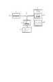
フラッシュメモリにデータを格納する使用例として特公平7−50558号公報に示すような半導体ディスクがある(図14を参照)。
このシステムでは、フラッシュメモリ4を半導体ディスクとして使用し、この半導体ディスクの制御を行うために制御装置1、RAM2、バス制御部3及び内部バス5が設けられているが、フラッシュメモリ4はEEPROMやSRAMにない制限がある。
【0006】
即ち、データの書き込みが0から1、または、1から0の一方通行である。このため、一度書き込みが完了した場所に再書き込みをする場合は、書き込みたい場所を含むブロックの全体を一括消去して、ブロック全体を0または1にした後、データの書き込みを行う必要がある。このため、EEPROMやSRAMのようにバイト単位で書き込みを行うことが難しい。
【0007】
【発明が解決しようとする課題】
従来の一括消去型不揮発性メモリは以上のように構成されているので、データの書込処理が実行された場所を含むブロックの全体を一括消去すれば、再度、同一の場所にデータを書き込むことができるが、フラッシュメモリの消去可能回数はEEPROMと比較して、10分の1程度しか保証されておらず、書換頻度の高いデータの記憶には対応することが困難であるなどの課題があった。
【0008】
この発明は上記のような課題を解決するためになされたもので、書換頻度の高いデータの記憶にも対応することができる一括消去型不揮発性メモリおよび携帯電話を得ることを目的とする。
【0009】
【課題を解決するための手段】
この発明に係る一括消去型不揮発性メモリは、複数のセクタから構成されるクラスタにおける未使用領域のアドレス情報を格納するアドレス情報格納手段と、データの書込要求を受けると、その未使用領域のアドレス情報を参照して、その未使用領域に当該データの書込処理を実行するデータ書込手段と、上記データ書込手段がデータの書込処理を実行すると、その未使用領域のアドレス情報を更新するアドレス情報更新手段とを備え、前記データ書込手段は、クラスタの未使用領域又は未使用クラスタに対するデータの書込エラーが発生すると、他の未使用クラスタにデータの書込処理を実行するとともに、データの書込エラーが発生したクラスタを一括消去することを特徴とする。
【0010】
この発明に係る携帯電話は、一括消去型不揮発性メモリを備える携帯電話であって、前記一括消去型不揮発性メモリは、複数のセクタから構成されるクラスタにおける未使用領域のアドレス情報を格納するアドレス情報格納手段と、データの書込要求を受けると、その未使用領域のアドレス情報を参照して、その未使用領域に当該データの書込処理を実行するデータ書込手段と、上記データ書込手段がデータの書込処理を実行すると、その未使用領域のアドレス情報を更新するアドレス情報更新手段と、を備え、前記データ書込手段は、クラスタの未使用領域又は未使用クラスタに対するデータの書込エラーが発生すると、他の未使用クラスタにデータの書込処理を実行するとともに、データの書込エラーが発生したクラスタを一括消去することを特徴とする。
【0023】
【発明の実施の形態】
以下、この発明の実施の一形態を説明する。
実施の形態1.
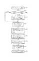
図1はこの発明の実施の形態1による一括消去型不揮発性メモリを示す構成図であり、図において、11は複数のセクタを有するクラスタから構成されるBGOフラッシュメモリ(アドレス情報格納手段)であり、BGOフラッシュメモリ11の先頭のセクタには未使用領域のアドレス情報が格納されている。12はBGOフラッシュメモリ11を制御するマイクロコンピュータ、13はマイクロコンピュータ12のRAM、14はマイクロコンピュータ12のCPUであり、CPU14は未使用領域のアドレス情報をBGOフラッシュメモリ11の先頭のセクタに格納するアドレス情報格納手段と、データの書込要求を受けると、そのクラスタにおける未使用領域のアドレス情報を参照して、その未使用領域にデータの書込処理を実行するデータ書込手段と、その未使用領域のアドレス情報を更新するアドレス情報更新手段と、各クラスタにIDを登録するID管理手段と、ポインタ構築手段とを構成する。
なお、図1のシステムの周辺には、本システムを使用する携帯電話などの周辺デバイスが接続される。
【0024】
次に動作について説明する。
最初に、図2を参照しながらBGOフラッシュメモリ11の物理アドレス、クラスタ管理エリア及びアプリケーションエリアについて説明する。ただし、BGOフラッシュメモリ11は、データを消去するとFFhになり、データの書き換え方向は1から0であるとする。
【0025】
クラスタ管理エリアのクラスタIDは、1バイトで表現され、00h及びFFhを除いた254通りの表現が可能である(アプリケーションが使用するクラスタにはユニークなIDが登録される)。
また、FFhが初期状態のためFFhが未使用クラスタID(FFhは書込可能なクラスタであることを示す)、00hが無効クラスタID(00hは書込不可能なクラスタであることを示す)となる。
図2の3個のクラスタIDには同じ値が格納され、2以上のクラスタIDが一致するとき、クラスタIDが有効であると判断する。
【0026】
3個のクラスタIDの次にはコピーフラグが1バイト確保され、消去ブロックのクラスタ管理エリアの4バイトを除いたエリアがアプリケーションエリアとなる。このアプリケーションエリアは、アプリケーションが自由に使用することができるエリアである。
【0027】
各アプリケーションは、自分のデータが格納されているアドレスを直接保持することはなく、自分のアプリケーションIDを保持している。制約事項として、このアプリケーションIDは、システムを使用する全てのアプリケーションにおいて唯一のものでなければならない。
実際にアプリケーションがBGOフラッシュメモリ11を使用する場合は、自分のアプリケーションIDに一致するクラスタIDを検索して、自分の使用している物理アドレスを検索し、そこからさらに、自分の読み書きしたいデータのアドレスを計算する。
【0028】
BGOフラッシュメモリ11は、データの消去をブロック単位で行う必要があるため、ブロック内のあるエリアのみを消去する場合は、必要データの待避、ブロックの消去、必要データの書き込みを行う必要がある。
必要データの待避をRAM13に行うことは、コストの面、BGOフラッシュメモリ11を使う意味、及びデータの信頼性からも望ましいものではない。
このためデータの待避は必然的にBGOフラッシュメモリ11上に行うが、そのためにはデータが書き込まれていない未使用領域、即ち、ブランクエリアが必要である。上記操作をデータリクレームと呼び、BGOフラッシュメモリ11において避けて通ることのできない処理である。
【0029】
ここで、図3及び図4を参照しながらデータリクレーム時の処理を説明する。
例えば、クラスタAのデータリクレームが必要になると(ステップST1)、クラスタAのアプリケーションは、BGOフラッシュメモリ11上のブランクエリアを検索する(ステップST2)。例えば、クラスタDがブランクエリアである場合には、クラスタDのクラスタIDを参照して、ブランクエリアのアドレスを取得する(ステップST4)。
ただし、ブランクエリアが存在しない場合には、無効クラスタを一括消去してブランクエリアを作成し(ステップST3)、そのブランクエリアのアドレスを取得する(ステップST4)。
【0030】
そして、ブランクエリアのアドレスを取得すると、クラスタAのアプリケーションは、現在使用中であるクラスタAのコピーフラグを01hにして(ステップST5)、ブランクエリア(クラスタD)に自分のアプリケーションID(1hのID)を登録する(ステップST6)。(図4の中段を参照)
【0031】
クラスタAのアプリケーションは、ブランクエリア(クラスタD)に自分のアプリケーションIDを登録すると、必要データをブランクエリアにコピーし(ステップST7)、コピーが完了すると、古いエリアであるクラスタAを一括消去または無効化して、処理を終了する(ステップST8,ST9)。(図4の下段を参照)
【0032】
ただし、データリクレーム中に電源遮断などの障害が発生すると、クラスタIDが同一のクラスタが存在してしまう場合がある。このような場合は、アプリケーションに割り振られたクラスタIDは重複できないという制約事項があるため、システム起動時に取り除く必要がある。
【0033】
このため、システム起動時に、重複クラスタの存在をチェックするが、重複クラスタを検出すると、重複クラスタのうち、コピーフラグがFFhであるものを削除する。その理由は、一括消去またはデータの無効化をする前に、システムの障害が発生すると、データリクレームの処理がどこまで完了したかを見極めることが困難である。そのため、コピーフラグを見てコピー元を判断し、コピー先を削除する。コピー元を保持しておけば、データの内容が壊れて書き込みが不可能になる不具合を回避することができるからである。
【0034】
次に、データの書き込み時にデバイスエラー(書込エラー)が発生すると、再度、データの書込処理を実行する必要がある。そのような場合に対処するために、ブランクエリアを2エリア以上用意しておくようにする。
また、データの書込エラーが発生すると、書込エラーが発生したクラスタIDを無効クラスタに変更して、新しいブランククラスタを取得し、リクレーム処理を実行する。無効クラスタにおいても、一旦、一括消去を行うと、クラスタの状態が元の正常な状態に戻る場合があるため、電源投入時や、システムが暇な時などに無効エリアを一括消去する。これは、デバイスの突発的なエラーに対して有効な手段である。
【0035】
図5はアプリケーションにおける内部データを示す構造図である。
クラスタはnページのセクタから構成されており、0ページ目にヘッダが確保され、1ページ目以降にデータエリアが確保されている。
このうち0ページの先頭4バイトはクラスタIDとコピー用フラグとして使用され、その後ろに32バイトの格納ページ情報が格納される。書き込むデータ長はシステムにて予め決定され、そのシステム内においては不変である。
【0036】
図7はデータの読み込み手順を示すものであるが、アプリケーションは、クラスタIDを参照して格納ページ情報を読み出し、データが格納されているセクタであるページ番号を取得する。
アプリケーションは、例えば、データがxページ目に格納されていることを認識すると、xページ目の先頭位置に格納されている格納位置オフセット情報を参照し、xページの何処にデータが格納されているかを認識する。
【0037】
ここで、格納ページ情報と格納位置オフセット情報は、ビットマップフィールドで表記され、両者とも32バイトのエリアを確保し、ビットが256個存在する。各ビットの値は、セクタの使用状態が変化するごとに、1から0に変更される。
【0038】
即ち、格納ページ情報については、例えば、1ページ目からxページ目までデータが格納されると、LSBからxビットまで、ビット値が1から0に変更され、0の数のトータルが指定ページに対応する。
一方、格納位置オフセット情報については、図6に示すように、データ領域の1バイトと、格納位置オフセット情報の1ビットが対応し、データ領域の先頭バイトから順次データが格納されるごとに、格納位置オフセット情報のLSBから順次1ビットが1から0に変更される。
【0039】
これにより、アプリケーションは、格納ページ情報における0のビットの合計からデータが格納されているページ番号を認識すると、格納位置オフセット情報のLSBから順次ビットの値をサーチして、データ領域の先頭からどこまでデータが格納されているかを認識する。
例えば、格納位置オフセット情報のLSBから24ビットまでが0の場合には、データ領域の先頭から24バイトまでデータが格納されていると認識する。
そして、アプリケーションは、データが格納されている最終位置を認識すると、そこからデータ長分前に戻った位置がデータの先頭アドレスであるので、その先頭アドレスからデータを読み出す処理を実行する。
【0040】
図8はデータの書込手順を示すフローチャートである。
まず、アプリケーションは、データの読み出し時と同じ手順で、データが格納されている最終位置を認識すると、そのページ内にブランクエリア(未使用領域)が存在するか否かを調査する(ステップST11)。
【0041】
ブランクエリアが存在する場合は、データが格納されている最終位置の次の位置を先頭アドレスとして、書込要求に係るデータの書込処理を実行するとともに、格納位置オフセット情報を更新する(ステップST12)。即ち、データが格納されている最終位置の次の位置に対応するビットを1から0に変更する。
【0042】
一方、現在のページ内にブランクエリアが存在しない場合、クラスタ内に次のページが存在するか否かを調査する(ステップST13)。
次のページが存在する場合には、次のページの格納位置オフセット情報を参照して、次のページがブランクであるか否かを調査する(ステップST14)。これは、次のページにおける過去のデータ書込時において、電源遮断等の障害が発生したことがあると、書込途中のデータが残っていることがあるからである(書込途中のデータが残っていると、新たなデータを書き込むことができない不具合が発生する)。
【0043】
アプリケーションは、次のページがブランクである場合には、データ領域の先頭位置に、書込要求に係るデータの書込処理を実行するとともに、格納位置オフセット情報を更新する(ステップST15)。また、アプリケーションは、格納ページ情報も更新する(ステップST16)。即ち、次のページに対応するビットを1から0に変更する。
【0044】
次のページがブランクでない場合には、更に次のページがブランクであるか否かを調査するが、次のページが存在しなくなると、上述したデータリクレームを実行して、他の未使用クラスタにおける1ページ目のデータ領域の先頭位置に、書込要求に係るデータの書込処理を実行する(ステップST17)。
【0045】
以上で明らかなように、この実施の形態1によれば、データの書込要求を受けると、未使用領域のアドレス情報を参照して、その未使用領域にデータの書込処理を実行するように構成したので、クラスタに未使用領域が存在する場合には、当該クラスタを一括消去することなく、データの書き込みが可能になり、その結果、BGOフラッシュメモリ11の書換回数が増加する効果を奏する。
【0046】
実施の形態2.
上記実施の形態1では、ページ内にブランクエリアが存在する場合、既に書き込まれているデータの後ろに詰めて最新のデータを書き込むものについて示したが、即ち、ページ内には複数のデータを格納する領域を確保して、最後に格納されたデータ(最新データ)のみを有効にするものについて示したが、図9に示すように、セクタ(ページ)内に複数のデータブロックを構成し、セクタのヘッダエリア内に格納されているデータブロックの使用状況を示す使用状況フラグ(ページ内使用中ブロックフラグ、ページ内使用済ブロックフラグ)を参照して、各データブロックの未使用領域にデータの書込処理を実行するようにしてもよい。
【0047】
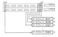
図9はアプリケーションにおける内部データを示す構造図である。
クラスタの全てにページヘッダと、複数個のデータブロックを作成する。ページヘッダにはクラスタIDと、コピー用フラグを先頭におき、その後ろにページ内使用中ブロックフラグを3バイト、ページ内使用済ブロックフラグを3バイトおく。
なお、データブロック内には、データNOとデータ領域使用状況を1バイトずつおき、その後ろ8バイトをデータ領域として使用する。
【0048】
図10はページ内使用中ブロックフラグ及びページ内使用済ブロックフラグとデータブロックの対応図である。
使用中のブロックを検索するには、ページ内使用中ブロックフラグとページ内使用済ブロックフラグの排他的論理和を求め、その結果が1のビットに対応するデータブロックが使用中のデータブロックになる(図10の例では、データブロックP)。
【0049】
データの読み書きは、データIDを指定することにより行う。
このうち、00hは使用済データIDとし、FFhはブランクデータIDとする。その他、254種類のデータIDをとることができる。各IDに割り振られるデータサイズは1バイトから8バイトまでの値をとることができ、プログラム中では、データサイズを変えることがないものとする。
【0050】
また、アプリケーションのポインタ構築手段がデータ検索用のポインタ(データを格納しているデータブロックのブロック位置を示すポインタ)をRAM13に作成する。ポインタの内部にはページ番号及びデータエリアのブロック番号を格納する。これを電源投入時などRAM13の内容が消えてしまったときに、全てのデータエリアをサーチして検索し、内容を保持する。
【0051】
読み出し時は、アプリケーションがデータIDのポインタが示すデータブロックを検索し、データ領域使用状況(図11を参照)を参照してデータの読込処理を実行する。
即ち、データ領域使用状況の8ビットがデータ領域の8バイトの使用状況に対応しており、データ領域使用状況のビットが0の場所が使用済の場所である。
【0052】
図12はデータ検索用ポインタの初期ルーチンを示すフローチャートである。
電源投入時などの初期ルーチンにおいては、アプリケーションが使用クラスタのアドレスを検索し、ページ内にデータがある場合には、ポインタのデータを更新する(ステップST21〜ST23)。
ページ内の使用データの検索方法であるが、全てのブロックを検索すると非常にデータ数が多いため、データの読込時と同様に、ページヘッダのページ内使用中ブロックフラグとページ内使用済ブロックフラグを参照して、使用データを検索する。
そして、全てのページの検索が終了するまで、上記の処理を繰り返し(ステップST24,ST25)、最後のページの検索が終了した時点でポインタの作成が完了する。
【0053】
図13はデータの書込手順を示すフローチャートである。
まず、アプリケーションは、データが格納されているデータブロックのブランクエリアを検索し、データを書き込むことができるブランクエリアがデータエリア内に存在する場合には、そのデータブロックのデータエリア(ブランクエリア)内にデータの書込処理を実行する(ステップST31,ST32)。
【0054】
一方、データを書き込むことができるブランクエリアがデータエリア内に存在しない場合には、他の新しいデータブロックを取得できるか否かを判断する(ステップST33)。
新しいデータブロックが取得できた場合、新しいデータブロックにデータNO、データ領域及びページ内使用中ブロックフラグを書き込む処理を実行する(ステップST34,ST35)。また、ページ内使用済ブロックフラグ及びデータブロックのIDの書込も同時に実行する(ステップST36,ST37)。なお、データブロックを新しく取得できない場合には、データリクレームを実行する(ステップST38)。
【0055】
以上で明らかなように、この実施の形態2によれば、セクタが複数のデータブロックから構成される場合、セクタのヘッダ領域内に格納されているデータブロックの使用状況を示す使用状況フラグ(ページ内使用中ブロックフラグ、ページ内使用済ブロックフラグ)等を参照して、そのデータブロックの未使用領域にデータの書込処理を実行するように構成したので、1バイトから8バイトの単位で、最大254種類のデータを自由に書き換えることができる効果を奏する。
【0056】
実施の形態3.
上記実施の形態1及び実施の形態2では、BGOフラッシュメモリ11にデータを書き込むものについて示したが、これに限るものではなく、その他の一括消去型不揮発性メモリにおいても使用可能であることは言うまでもない。
【0057】
【発明の効果】
以上のように、この発明によれば、クラスタの未使用領域又は未使用クラスタに対するデータの書込エラーが発生すると、他の未使用クラスタにデータの書込処理を実行するとともに、データの書込エラーが発生したクラスタを一括消去するように構成したので、データの書込エラーが発生しても、データの書込処理を実行することができる効果がある。
【図面の簡単な説明】
【図1】 この発明の実施の形態1による一括消去型不揮発性メモリを示す構成図である。
【図2】 BGOフラッシュメモリの内部構造及びクラスタ管理エリアを示す説明図である。
【図3】 データリクレームの処理を示すフローチャートである。
【図4】 データリクレーム時におけるクラスタIDの割り当てを示す説明図である。
【図5】 アプリケーションにおける内部データを示す構造図である。
【図6】 格納位置オフセット情報とデータの対応関係を示す説明図である。
【図7】 データの読み込み手順を示す説明図である。
【図8】 データの書込手順を示すフローチャートである。
【図9】 アプリケーションにおける内部データを示す構造図である。
【図10】 ページ内使用中ブロックフラグ及びページ内使用済ブロックフラグとデータブロックの対応図である。
【図11】 データ領域使用状況とデータ領域の対応図である。
【図12】 データ検索用ポインタの初期ルーチンを示すフローチャートである。
【図13】 データの書込手順を示すフローチャートである。
【図14】 フラッシュメモリにデータを格納する半導体ディスクを示す構成図である。
【符号の説明】
11 BGOフラッシュメモリ(アドレス情報格納手段)、14 CPU(アドレス情報格納手段、データ書込手段、アドレス情報更新手段、ID管理手段、ポインタ構築手段)。[0001]
BACKGROUND OF THE INVENTION
The present invention relates to a batch erasing nonvolatile memory such as a flash EEPROM (hereinafter referred to as a flash memory) for recording nonvolatile dataand a mobile phone .
[0002]
[Prior art]
In current embedded systems such as mobile phones, when storing system programs, a flash memory that can be randomly accessed is used, while data that is frequently rewritten or non-volatile data that has a relatively small amount of data is recorded. In this case, an EEPROM is used, and when a large amount of nonvolatile data is recorded, a flash memory by serial writing or an SRAM with a backup power source is used.
[0003]
Here, the EEPROM has a larger number of storage elements per bit than the flash memory, and the unit price per bit increases. In addition, the SRAM with a backup power supply increases the cost because it is powered. By storing the data stored separately in the flash memory, there is an advantage that the mounting area and cost of the device are reduced.
[0004]
The conventional flash memory in the embedded system cannot read other system programs during the execution of the system program writing process, and writes the program by performing a special process when writing the system program. However, recently, with the advent of a batch erasable nonvolatile memory (hereinafter referred to as a BGO flash memory) that can read data from other areas where data has not been written during the execution of data writing processing, It is now possible to load the flash memory that stores the program into the flash memory that stores the program.
[0005]
As a use example of storing data in a flash memory, there is a semiconductor disk as shown in Japanese Patent Publication No. 7-50558 (see FIG. 14).
In this system, a
[0006]
That is, data writing is one-way from 0 to 1 or 1 to 0. For this reason, when rewriting to a place where writing has been completed once, it is necessary to erase the entire block including the place to be written at once and set the entire block to 0 or 1 before writing data. For this reason, it is difficult to perform writing in byte units as in EEPROM and SRAM.
[0007]
[Problems to be solved by the invention]
Since the conventional batch erasing type nonvolatile memory is configured as described above, if the entire block including the place where the data writing process is executed is batch erased, the data is written again to the same location. However, the number of erasable times of the flash memory is only guaranteed about one-tenth that of an EEPROM, and there is a problem that it is difficult to cope with storing data with a high rewrite frequency. It was.
[0008]
The present invention has been made to solve the above-described problems, and an object of the present invention is to obtain a collective erasing nonvolatile memoryand a mobile phone that can cope with storage of data with a high rewrite frequency.
[0009]
[Means for Solving the Problems]
The collective erasure type nonvolatile memory according to the present invention includesan address information storage means for storing address information of an unused area in a cluster composed of aplurality of sectors, and when the data write request is received, By referring to the address information, the data writing means for executing the data writing process in the unused area, and when the data writing means executes the data writing process, the address information of the unused area is obtained. Address information updating means for updating, and when the data writing error occurs in an unused area of the cluster or an unused cluster, the data writing means executes a data writing process to another unused cluster. At the same time, a cluster in which a data write error has occurred is erased collectively.
[0010]
Thecellular phone according to the present invention is acellular phone provided with a batch erasing nonvolatile memory, and the batch erasing nonvolatile memory is an address for storing address information of an unused area in a cluster composed of a plurality of sectors. An information storage means, a data writing means for referring to address information of the unused area when receiving a data write request, and executing the data writing process in the unused area, and the data writing And means for updating the address information of the unused area when the means executes the data writing process, wherein the data writing means writes the data to the unused area of the cluster or to the unused cluster. When a data write error occurs, data is written to other unused clusters and the cluster in which the data write error has occurred is erased at once. And wherein the door.
[0023]
DETAILED DESCRIPTION OF THE INVENTION
An embodiment of the present invention will be described below.
FIG. 1 is a block diagram showing a batch erase type nonvolatile memory according to
1 is connected to peripheral devices such as a mobile phone using the system.
[0024]
Next, the operation will be described.
First, the physical address, cluster management area, and application area of the
[0025]
The cluster ID of the cluster management area is expressed by 1 byte and can be expressed in 254 ways excluding 00h and FFh (a unique ID is registered in the cluster used by the application).
Also, since FFh is in an initial state, FFh is an unused cluster ID (FFh indicates a writable cluster), 00h is an invalid cluster ID (00h indicates a non-writable cluster), and Become.
The same value is stored in the three cluster IDs in FIG. 2, and when two or more cluster IDs match, it is determined that the cluster ID is valid.
[0026]
Next to the three cluster IDs, 1 byte of the copy flag is secured, and the area excluding the 4 bytes of the cluster management area of the erase block becomes the application area. This application area is an area that an application can use freely.
[0027]
Each application does not directly hold an address where its own data is stored, but holds its own application ID. As a restriction, this application ID must be unique for all applications using the system.
When an application actually uses the
[0028]
Since the
Saving the necessary data to the
For this reason, data is inevitably saved on the
[0029]
Here, processing at the time of data reclaim will be described with reference to FIGS. 3 and 4.
For example, when data reclaim for cluster A becomes necessary (step ST1), the application of cluster A searches for a blank area on the BGO flash memory 11 (step ST2). For example, if the cluster D is a blank area, the address of the blank area is acquired with reference to the cluster ID of the cluster D (step ST4).
However, if there is no blank area, the invalid cluster is erased collectively to create a blank area (step ST3), and the address of the blank area is acquired (step ST4).
[0030]
When the address of the blank area is acquired, the application of cluster A sets the copy flag of cluster A currently in use to 01h (step ST5), and its own application ID (ID of 1h) is assigned to the blank area (cluster D). ) Is registered (step ST6). (Refer to the middle of Figure 4)
[0031]
When the application of cluster A registers its own application ID in the blank area (cluster D), the necessary data is copied to the blank area (step ST7). When the copying is completed, the cluster A which is the old area is erased or invalidated. And the process ends (steps ST8 and ST9). (See the lower part of Fig. 4)
[0032]
However, if a failure such as power interruption occurs during data reclaim, a cluster with the same cluster ID may exist. In such a case, there is a restriction that the cluster ID assigned to the application cannot be duplicated, so it is necessary to remove it when the system is started.
[0033]
For this reason, the presence of duplicate clusters is checked when the system is activated. If duplicate clusters are detected, those having a copy flag of FFh among the duplicate clusters are deleted. The reason is that it is difficult to determine how far the data reclaim processing has been completed if a system failure occurs before batch erasure or data invalidation. Therefore, the copy source is determined by looking at the copy flag, and the copy destination is deleted. This is because if the copy source is held, it is possible to avoid a problem that the data contents are broken and cannot be written.
[0034]
Next, when a device error (write error) occurs during data writing, it is necessary to execute data writing processing again. In order to cope with such a case, two or more blank areas are prepared.
When a data write error occurs, the cluster ID in which the write error has occurred is changed to an invalid cluster, a new blank cluster is acquired, and reclaim processing is executed. Even in the invalid cluster, once the collective erasure is performed, the cluster state may return to the original normal state. Therefore, the invalid area is erased collectively when the power is turned on or the system is idle. This is an effective means against sudden errors in the device.
[0035]
FIG. 5 is a structural diagram showing internal data in the application.
The cluster is composed of sectors of n pages, a header is secured on the 0th page, and a data area is secured on and after the first page.
Of these, the first 4 bytes of page 0 are used as a cluster ID and a copy flag, followed by 32 bytes of stored page information. The length of data to be written is predetermined by the system and is not changed in the system.
[0036]
FIG. 7 shows a data reading procedure. The application reads the storage page information with reference to the cluster ID, and acquires the page number that is the sector in which the data is stored.
For example, when the application recognizes that the data is stored in the x page, the application refers to the storage position offset information stored in the head position of the x page, and where the data is stored in the x page. Recognize
[0037]
Here, the storage page information and the storage position offset information are represented by a bitmap field, both of which secure an area of 32 bytes and have 256 bits. The value of each bit is changed from 1 to 0 every time the use state of the sector changes.
[0038]
That is, for the stored page information, for example, when data is stored from the first page to the x page, the bit value is changed from 1 to 0 from LSB to x bit, and the total number of 0 is stored in the designated page. Correspond.
On the other hand, as shown in FIG. 6, the storage position offset information corresponds to one byte of the data area and one bit of the storage position offset information, and is stored every time data is sequentially stored from the first byte of the data area. One bit is sequentially changed from 1 to 0 from the LSB of the position offset information.
[0039]
As a result, when the application recognizes the page number in which the data is stored from the total of 0 bits in the stored page information, the application sequentially searches for the value of the bit from the LSB of the storage position offset information, and from where it starts from the beginning of the data area. Recognizes whether data is stored.
For example, when the storage position offset information from the LSB to 24 bits is 0, it is recognized that data is stored from the head of the data area to 24 bytes.
Then, when the application recognizes the final position where the data is stored, since the position returned by the data length from that position is the start address of the data, the application executes a process of reading data from the start address.
[0040]
FIG. 8 is a flowchart showing a data writing procedure.
First, when the application recognizes the final position where data is stored in the same procedure as when reading data, it checks whether or not a blank area (unused area) exists in the page (step ST11). .
[0041]
If there is a blank area, the next position after the last position where the data is stored is used as the head address, the data writing process related to the write request is executed, and the storage position offset information is updated (step ST12). ). That is, the bit corresponding to the position next to the final position where data is stored is changed from 1 to 0.
[0042]
On the other hand, if there is no blank area in the current page, it is investigated whether or not the next page exists in the cluster (step ST13).
If the next page exists, the storage position offset information of the next page is referred to and it is checked whether or not the next page is blank (step ST14). This is because during the past data writing in the next page, if a failure such as a power interruption has occurred, the data being written may remain (the data being written is If it remains, there will be a problem that new data cannot be written.)
[0043]
If the next page is blank, the application executes the data write processing related to the write request at the start position of the data area and updates the storage position offset information (step ST15). The application also updates the stored page information (step ST16). That is, the bit corresponding to the next page is changed from 1 to 0.
[0044]
If the next page is not blank, it is further investigated whether the next page is blank, but if the next page does not exist, the above-mentioned data reclaim is executed and another unused cluster is checked. In step ST17, data write processing relating to the write request is executed at the head position of the data area of the first page.
[0045]
As is apparent from the above, according to the first embodiment, when a data write request is received, the address information of the unused area is referred to and the data write process is executed in the unused area. Thus, when an unused area exists in a cluster, data can be written without erasing the cluster at once, and as a result, the number of rewrites of the
[0046]
In the first embodiment, when there is a blank area in the page, the latest data is written after the already written data. That is, a plurality of data is stored in the page. As shown in FIG. 9, a plurality of data blocks are configured in a sector (page) as shown in FIG. 9, and only the last stored data (latest data) is validated. Referring to the usage flag (in-page used block flag, in-page used block flag) indicating the usage status of the data block stored in the header area, data is written to the unused area of each data block. May be executed.
[0047]
FIG. 9 is a structural diagram showing internal data in the application.
Create page headers and multiple data blocks for all clusters. In the page header, a cluster ID and a copy flag are placed at the head, followed by an in-page in-use block flag of 3 bytes and an in-page used block flag of 3 bytes.
In the data block, the data NO and the data area usage status are set 1 byte each, and the subsequent 8 bytes are used as the data area.
[0048]
FIG. 10 is a correspondence diagram of the in-page in-use block flag, the in-page used block flag, and the data block.
To search for a block in use, an exclusive OR of the in-page in-use block flag and the in-page in-use block flag is obtained, and the data block corresponding to the 1 bit becomes the in-use data block. (Data block P in the example of FIG. 10).
[0049]
Data is read and written by designating a data ID.
Of these, 00h is used data ID, and FFh is blank data ID. In addition, 254 types of data IDs can be taken. The data size allocated to each ID can take a value from 1 byte to 8 bytes, and the data size is not changed in the program.
[0050]
In addition, the pointer construction means of the application creates a pointer for data retrieval (a pointer indicating the block position of the data block storing the data) in the
[0051]
At the time of reading, the application searches for the data block indicated by the pointer of the data ID, and executes the data reading process with reference to the data area usage status (see FIG. 11).
That is, 8 bits in the data area usage status correspond to the usage status of 8 bytes in the data area, and a location where the data area usage status bit is 0 is a used location.
[0052]
FIG. 12 is a flowchart showing an initial routine for a data search pointer.
In an initial routine such as when the power is turned on, the application searches for the address of the cluster to be used, and if there is data in the page, the pointer data is updated (steps ST21 to ST23).
This is a search method of used data in the page, but if all blocks are searched, the number of data is very large. Therefore, as in the case of reading data, the in-page used block flag and the used block flag in the page header Refer to and search for usage data.
Then, the above process is repeated until the search for all pages is completed (steps ST24 and ST25), and the creation of the pointer is completed when the search for the last page is completed.
[0053]
FIG. 13 is a flowchart showing a data writing procedure.
First, the application searches for a blank area of a data block in which data is stored. If there is a blank area in the data area where data can be written, the application stores the data block (blank area) in the data block. The data writing process is executed (steps ST31 and ST32).
[0054]
On the other hand, if there is no blank area in the data area where data can be written, it is determined whether another new data block can be acquired (step ST33).
When a new data block can be acquired, a process of writing the data NO, the data area, and the in-page in-use block flag to the new data block is executed (steps ST34 and ST35). The in-page used block flag and the data block ID are simultaneously written (steps ST36 and ST37). If a new data block cannot be acquired, data reclaim is executed (step ST38).
[0055]
As apparent from the above, according to the second embodiment, when a sector is composed of a plurality of data blocks, a usage status flag (page) indicating the usage status of the data block stored in the header area of the sector. (In-use block flag, in-page used block flag), etc., so that the data writing process is executed in the unused area of the data block, so in units of 1 to 8 bytes, There is an effect that a maximum of 254 types of data can be freely rewritten.
[0056]
In the first embodiment and the second embodiment, the data write to the
[0057]
【The invention's effect】
As described above, according to the present invention, whena data write error occurs in an unused area of acluster or an unused cluster, data writing processing is performed on another unused cluster and data writing is performed. Since the cluster in which the error has occurred is configured to be erased at once, there is an effectthat the data writing process can be executed even if a data writing error occurs .
[Brief description of the drawings]
FIG. 1 is a block diagram showing a batch erase nonvolatile memory according to a first embodiment of the present invention.
FIG. 2 is an explanatory diagram showing an internal structure of a BGO flash memory and a cluster management area.
FIG. 3 is a flowchart showing data reclaim processing;
FIG. 4 is an explanatory diagram showing cluster ID assignment at the time of data reclaim.
FIG. 5 is a structural diagram showing internal data in an application.
FIG. 6 is an explanatory diagram showing a correspondence relationship between storage position offset information and data.
FIG. 7 is an explanatory diagram showing a data reading procedure;
FIG. 8 is a flowchart showing a data writing procedure.
FIG. 9 is a structural diagram showing internal data in an application.
FIG. 10 is a correspondence diagram of in-page in-use block flags and in-page used block flags and data blocks.
FIG. 11 is a correspondence diagram between data area usage statuses and data areas;
FIG. 12 is a flowchart showing an initial routine for a data search pointer.
FIG. 13 is a flowchart showing a data writing procedure.
FIG. 14 is a configuration diagram showing a semiconductor disk for storing data in a flash memory.
[Explanation of symbols]
11 BGO flash memory (address information storage means), 14 CPU (address information storage means, data writing means, address information update means, ID management means, pointer construction means).
Claims (6)
Translated fromJapaneseデータの書込要求を受けると、その未使用領域のアドレス情報を参照して、その未使用領域に当該データの書込処理を実行するデータ書込手段と、
上記データ書込手段がデータの書込処理を実行すると、その未使用領域のアドレス情報を更新するアドレス情報更新手段と、
を備え、
前記データ書込手段は、クラスタの未使用領域又は未使用クラスタに対するデータの書込エラーが発生すると、他の未使用クラスタにデータの書込処理を実行するとともに、データの書込エラーが発生したクラスタを一括消去することを特徴とする一括消去型不揮発性メモリ。Address information storage means for storing address information of unused areas in a cluster composed of a plurality of sectors;
When receiving a data write request, referring to the address information of the unused area, data writing means for executing the data writing process in the unused area,
When the data writing means executes data writing processing, address information updating means for updating address information of the unused area;
Equipped witha,
When an error in writing data to an unused area of a cluster or an unused cluster occurs, the data writing means executes a data writing process on another unused cluster, and a data writing error occurs. Batch erase type non-volatile memorycharacterized by batch erasing clusters .
前記一括消去型不揮発性メモリは、The batch erasing nonvolatile memory is
複数のセクタから構成されるクラスタにおける未使用領域のアドレス情報を格納するアドレス情報格納手段と、Address information storage means for storing address information of unused areas in a cluster composed of a plurality of sectors;
データの書込要求を受けると、その未使用領域のアドレス情報を参照して、その未使用領域に当該データの書込処理を実行するデータ書込手段と、Upon receiving a data write request, data writing means for referring to address information of the unused area and executing the data writing process in the unused area;
上記データ書込手段がデータの書込処理を実行すると、その未使用領域のアドレス情報を更新するアドレス情報更新手段と、When the data writing means executes data writing processing, address information updating means for updating address information of the unused area;
を備え、With
前記データ書込手段は、クラスタの未使用領域又は未使用クラスタに対するデータの書込エラーが発生すると、他の未使用クラスタにデータの書込処理を実行するとともに、データの書込エラーが発生したクラスタを一括消去することを特徴とする携帯電話。When an error in writing data to an unused area of a cluster or an unused cluster occurs, the data writing means executes a data writing process on another unused cluster and a data writing error occurs. A mobile phone characterized by erasing clusters at once.
Priority Applications (6)
| Application Number | Priority Date | Filing Date | Title |
|---|---|---|---|
| JP35503598AJP4046877B2 (en) | 1998-12-14 | 1998-12-14 | Batch erase nonvolatile memory and mobile phone |
| US09/318,791US6839798B1 (en) | 1998-12-14 | 1999-05-26 | Flash memory capable of storing frequently rewritten data |
| TW088120207ATW454119B (en) | 1998-12-14 | 1999-11-19 | Batch erasable non-volatile memory and the control method |
| KR10-1999-0057353AKR100370893B1 (en) | 1998-12-14 | 1999-12-14 | Flash memory unit and control method of flash memory |
| DE19960258ADE19960258A1 (en) | 1998-12-14 | 1999-12-14 | Flash memory unit for storing address information, has data writing unit for writing addresses in black areas of memory cluster, and address updating unit |
| CNB991267354ACN1149487C (en) | 1998-12-14 | 1999-12-14 | Batch erasable nonvolatile memory and control method of flash memory |
Applications Claiming Priority (1)
| Application Number | Priority Date | Filing Date | Title |
|---|---|---|---|
| JP35503598AJP4046877B2 (en) | 1998-12-14 | 1998-12-14 | Batch erase nonvolatile memory and mobile phone |
Related Child Applications (1)
| Application Number | Title | Priority Date | Filing Date |
|---|---|---|---|
| JP2007279010ADivisionJP4794530B2 (en) | 2007-10-26 | 2007-10-26 | Semiconductor device and mobile phone |
Publications (2)
| Publication Number | Publication Date |
|---|---|
| JP2000182381A JP2000182381A (en) | 2000-06-30 |
| JP4046877B2true JP4046877B2 (en) | 2008-02-13 |
Family
ID=18441548
Family Applications (1)
| Application Number | Title | Priority Date | Filing Date |
|---|---|---|---|
| JP35503598AExpired - Fee RelatedJP4046877B2 (en) | 1998-12-14 | 1998-12-14 | Batch erase nonvolatile memory and mobile phone |
Country Status (6)
| Country | Link |
|---|---|
| US (1) | US6839798B1 (en) |
| JP (1) | JP4046877B2 (en) |
| KR (1) | KR100370893B1 (en) |
| CN (1) | CN1149487C (en) |
| DE (1) | DE19960258A1 (en) |
| TW (1) | TW454119B (en) |
Families Citing this family (23)
| Publication number | Priority date | Publication date | Assignee | Title |
|---|---|---|---|---|
| EP1659758A1 (en)* | 2000-04-26 | 2006-05-24 | Semiconductor Energy Laboratory Co., Ltd. | A communication method for identifying an individual by means of biological information |
| JP2002035381A (en)* | 2000-07-28 | 2002-02-05 | Shinobu Hidaka | Pachinko ball management system, pachinko game console and pachinko card |
| CN1459112A (en)* | 2001-07-17 | 2003-11-26 | 三菱电机株式会社 | Storage device |
| US8504798B2 (en)* | 2003-12-30 | 2013-08-06 | Sandisk Technologies Inc. | Management of non-volatile memory systems having large erase blocks |
| US7631138B2 (en)* | 2003-12-30 | 2009-12-08 | Sandisk Corporation | Adaptive mode switching of flash memory address mapping based on host usage characteristics |
| TWI266291B (en)* | 2004-07-23 | 2006-11-11 | Mediatek Inc | Method and apparatus of blank detection for optical storage disk |
| CN100481267C (en)* | 2004-08-09 | 2009-04-22 | 凌阳科技股份有限公司 | Method for using nonvolatile memory and electronic device thereof |
| CN100442246C (en)* | 2004-08-26 | 2008-12-10 | 旺玖科技股份有限公司 | Data updating method of nonvolatile memory |
| JP4715155B2 (en)* | 2004-10-08 | 2011-07-06 | ソニー株式会社 | Information processing apparatus, information processing method, and computer program |
| JP2009521045A (en)* | 2005-12-21 | 2009-05-28 | エヌエックスピー ビー ヴィ | Nonvolatile memory having block erasable memory locations |
| US7668018B2 (en)* | 2007-04-03 | 2010-02-23 | Freescale Semiconductor, Inc. | Electronic device including a nonvolatile memory array and methods of using the same |
| US7877541B2 (en)* | 2007-12-22 | 2011-01-25 | Unity Semiconductor Corporation | Method and system for accessing non-volatile memory |
| JP2009288963A (en)* | 2008-05-28 | 2009-12-10 | Sanyo Electric Co Ltd | Data writing device and program |
| US7917803B2 (en)* | 2008-06-17 | 2011-03-29 | Seagate Technology Llc | Data conflict resolution for solid-state memory devices |
| US8321764B2 (en) | 2008-12-11 | 2012-11-27 | Micron Technology, Inc. | Multilevel encoding with error correction |
| JP5533141B2 (en)* | 2010-03-31 | 2014-06-25 | アイシン・エィ・ダブリュ株式会社 | Writing device, writing method, and writing program |
| FR2959586B1 (en)* | 2010-04-30 | 2012-06-22 | Proton World Int Nv | METHOD OF WRITING AND READING IN AN ATOMICITY MEMORY |
| US9116895B1 (en) | 2011-08-25 | 2015-08-25 | Infotech International Llc | Document processing system and method |
| US9785638B1 (en) | 2011-08-25 | 2017-10-10 | Infotech International Llc | Document display system and method |
| US9633012B1 (en) | 2011-08-25 | 2017-04-25 | Infotech International Llc | Construction permit processing system and method |
| JP7112060B2 (en) | 2018-12-26 | 2022-08-03 | ルネサスエレクトロニクス株式会社 | Semiconductor device and its power control method |
| CN112181303B (en)* | 2020-09-29 | 2024-08-16 | 广东艾科技术股份有限公司 | Data storage method, device, computer equipment and storage medium |
| CN115686379B (en)* | 2022-12-14 | 2024-02-20 | 江苏华存电子科技有限公司 | Method and system for optimizing management of hollow white data area in flash memory |
Family Cites Families (9)
| Publication number | Priority date | Publication date | Assignee | Title |
|---|---|---|---|---|
| US5438573A (en) | 1991-09-13 | 1995-08-01 | Sundisk Corporation | Flash EEPROM array data and header file structure |
| US5404485A (en) | 1993-03-08 | 1995-04-04 | M-Systems Flash Disk Pioneers Ltd. | Flash file system |
| JPH06332806A (en) | 1993-05-25 | 1994-12-02 | Hitachi Ltd | Storage system with flash memory as storage medium and control method therefor |
| JPH0750558A (en) | 1993-08-04 | 1995-02-21 | Seiko Epson Corp | Logic circuit |
| JP3154892B2 (en)* | 1994-05-10 | 2001-04-09 | 株式会社東芝 | IC memory card and inspection method of the IC memory card |
| JPH08137634A (en) | 1994-11-09 | 1996-05-31 | Mitsubishi Electric Corp | Flash disk card |
| GB2291991A (en) | 1995-09-27 | 1996-02-07 | Memory Corp Plc | Disk drive emulation with a block-erasable memory |
| JP3615299B2 (en)* | 1996-03-29 | 2005-02-02 | 三洋電機株式会社 | Rewriteable ROM storage method and storage device |
| US6038636A (en)* | 1998-04-27 | 2000-03-14 | Lexmark International, Inc. | Method and apparatus for reclaiming and defragmenting a flash memory device |
- 1998
- 1998-12-14JPJP35503598Apatent/JP4046877B2/ennot_activeExpired - Fee Related
- 1999
- 1999-05-26USUS09/318,791patent/US6839798B1/ennot_activeExpired - Fee Related
- 1999-11-19TWTW088120207Apatent/TW454119B/ennot_activeIP Right Cessation
- 1999-12-14KRKR10-1999-0057353Apatent/KR100370893B1/ennot_activeExpired - Fee Related
- 1999-12-14CNCNB991267354Apatent/CN1149487C/ennot_activeExpired - Fee Related
- 1999-12-14DEDE19960258Apatent/DE19960258A1/ennot_activeCeased
Also Published As
| Publication number | Publication date |
|---|---|
| CN1258046A (en) | 2000-06-28 |
| CN1149487C (en) | 2004-05-12 |
| KR100370893B1 (en) | 2003-02-05 |
| JP2000182381A (en) | 2000-06-30 |
| KR20000048112A (en) | 2000-07-25 |
| TW454119B (en) | 2001-09-11 |
| DE19960258A1 (en) | 2000-06-21 |
| US6839798B1 (en) | 2005-01-04 |
Similar Documents
| Publication | Publication Date | Title |
|---|---|---|
| JP4046877B2 (en) | Batch erase nonvolatile memory and mobile phone | |
| JP3692313B2 (en) | Nonvolatile memory control method | |
| US6865658B2 (en) | Nonvolatile data management system using data segments and link information | |
| USRE45222E1 (en) | Method of writing of writing to a flash memory including data blocks and log blocks, using a logical address having a block address portion and page identifying portion, a block address table and a page table | |
| US6687784B2 (en) | Controller for controlling nonvolatile memory unit | |
| JP4633802B2 (en) | Nonvolatile storage device, data read method, and management table creation method | |
| KR0128218B1 (en) | Nonvolatile memory with flash erase capability | |
| JP4524309B2 (en) | Memory controller for flash memory | |
| US8041884B2 (en) | Controller for non-volatile memories and methods of operating the memory controller | |
| JP3485938B2 (en) | Nonvolatile semiconductor memory device | |
| EP1548602B1 (en) | Non-volatile storage device control method | |
| JP2004152302A (en) | Method and apparatus for performing a block cache in a non-volatile memory system | |
| JP2002508862A (en) | Moving sectors in blocks in flash memory | |
| KR20080037283A (en) | System comprising flash memory device and data recovery method thereof | |
| JP4301301B2 (en) | Nonvolatile semiconductor memory device and management method thereof | |
| US20060018227A1 (en) | Controller, data memory system, data rewriting method, and computer program product | |
| JP4794530B2 (en) | Semiconductor device and mobile phone | |
| JP4242245B2 (en) | Flash ROM control device | |
| CN115878033A (en) | Solid state disk and mapping table management method thereof | |
| JPH11272569A (en) | Data recovery method for external storage device using flash memory | |
| JP3826115B2 (en) | Storage device, memory management method, and program | |
| JP7219813B2 (en) | Arithmetic processing device, vehicle control device and update method | |
| JP2004326523A (en) | Storage device having rewritable nonvolatile memory and method of controlling nonvolatile memory for storage device | |
| JP4661369B2 (en) | Memory controller | |
| JP3670151B2 (en) | Flash memory access method, system including driver for accessing flash memory, and flash memory |
Legal Events
| Date | Code | Title | Description |
|---|---|---|---|
| A621 | Written request for application examination | Free format text:JAPANESE INTERMEDIATE CODE: A621 Effective date:20050406 | |
| RD01 | Notification of change of attorney | Free format text:JAPANESE INTERMEDIATE CODE: A7421 Effective date:20060223 | |
| RD01 | Notification of change of attorney | Free format text:JAPANESE INTERMEDIATE CODE: A7421 Effective date:20060310 | |
| A131 | Notification of reasons for refusal | Free format text:JAPANESE INTERMEDIATE CODE: A131 Effective date:20070828 | |
| A521 | Written amendment | Free format text:JAPANESE INTERMEDIATE CODE: A523 Effective date:20071026 | |
| TRDD | Decision of grant or rejection written | ||
| A01 | Written decision to grant a patent or to grant a registration (utility model) | Free format text:JAPANESE INTERMEDIATE CODE: A01 Effective date:20071120 | |
| A61 | First payment of annual fees (during grant procedure) | Free format text:JAPANESE INTERMEDIATE CODE: A61 Effective date:20071121 | |
| FPAY | Renewal fee payment (event date is renewal date of database) | Free format text:PAYMENT UNTIL: 20101130 Year of fee payment:3 | |
| R150 | Certificate of patent or registration of utility model | Free format text:JAPANESE INTERMEDIATE CODE: R150 | |
| FPAY | Renewal fee payment (event date is renewal date of database) | Free format text:PAYMENT UNTIL: 20111130 Year of fee payment:4 | |
| FPAY | Renewal fee payment (event date is renewal date of database) | Free format text:PAYMENT UNTIL: 20111130 Year of fee payment:4 | |
| S111 | Request for change of ownership or part of ownership | Free format text:JAPANESE INTERMEDIATE CODE: R313115 | |
| FPAY | Renewal fee payment (event date is renewal date of database) | Free format text:PAYMENT UNTIL: 20111130 Year of fee payment:4 | |
| R350 | Written notification of registration of transfer | Free format text:JAPANESE INTERMEDIATE CODE: R350 | |
| FPAY | Renewal fee payment (event date is renewal date of database) | Free format text:PAYMENT UNTIL: 20111130 Year of fee payment:4 | |
| FPAY | Renewal fee payment (event date is renewal date of database) | Free format text:PAYMENT UNTIL: 20121130 Year of fee payment:5 | |
| FPAY | Renewal fee payment (event date is renewal date of database) | Free format text:PAYMENT UNTIL: 20121130 Year of fee payment:5 | |
| FPAY | Renewal fee payment (event date is renewal date of database) | Free format text:PAYMENT UNTIL: 20131130 Year of fee payment:6 | |
| S531 | Written request for registration of change of domicile | Free format text:JAPANESE INTERMEDIATE CODE: R313531 | |
| R350 | Written notification of registration of transfer | Free format text:JAPANESE INTERMEDIATE CODE: R350 | |
| LAPS | Cancellation because of no payment of annual fees |