JP4045878B2 - Color filter substrate, electro-optical device, and electronic apparatus - Google Patents
Color filter substrate, electro-optical device, and electronic apparatusDownload PDFInfo
- Publication number
- JP4045878B2 JP4045878B2JP2002195214AJP2002195214AJP4045878B2JP 4045878 B2JP4045878 B2JP 4045878B2JP 2002195214 AJP2002195214 AJP 2002195214AJP 2002195214 AJP2002195214 AJP 2002195214AJP 4045878 B2JP4045878 B2JP 4045878B2
- Authority
- JP
- Japan
- Prior art keywords
- substrate
- shielding layer
- light
- reflective film
- light shielding
- Prior art date
- Legal status (The legal status is an assumption and is not a legal conclusion. Google has not performed a legal analysis and makes no representation as to the accuracy of the status listed.)
- Expired - Fee Related
Links
- 239000000758substrateSubstances0.000titleclaimsdescription181
- 239000004973liquid crystal related substanceSubstances0.000claimsdescription58
- 239000011347resinSubstances0.000claimsdescription14
- 229920005989resinPolymers0.000claimsdescription14
- 238000000638solvent extractionMethods0.000claimsdescription5
- 239000010408filmSubstances0.000description133
- 238000000034methodMethods0.000description31
- 238000004519manufacturing processMethods0.000description23
- 239000011159matrix materialSubstances0.000description10
- 238000000206photolithographyMethods0.000description8
- 238000012986modificationMethods0.000description7
- 230000004048modificationEffects0.000description7
- 238000005530etchingMethods0.000description6
- 239000000049pigmentSubstances0.000description6
- 230000015572biosynthetic processEffects0.000description5
- 239000003822epoxy resinSubstances0.000description5
- 239000011521glassSubstances0.000description5
- 239000000463materialSubstances0.000description5
- 229920000647polyepoxidePolymers0.000description5
- 239000010409thin filmSubstances0.000description5
- 239000004925Acrylic resinSubstances0.000description4
- 229920000178Acrylic resinPolymers0.000description4
- 229910052751metalInorganic materials0.000description4
- 239000002184metalSubstances0.000description4
- 238000004528spin coatingMethods0.000description4
- 230000000694effectsEffects0.000description3
- 239000004033plasticSubstances0.000description3
- 239000003566sealing materialSubstances0.000description3
- 238000004544sputter depositionMethods0.000description3
- 239000004642PolyimideSubstances0.000description2
- 229910052782aluminiumInorganic materials0.000description2
- XAGFODPZIPBFFR-UHFFFAOYSA-NaluminiumChemical compound[Al]XAGFODPZIPBFFR-UHFFFAOYSA-N0.000description2
- 239000004020conductorSubstances0.000description2
- 238000009792diffusion processMethods0.000description2
- 238000005401electroluminescenceMethods0.000description2
- 238000005286illuminationMethods0.000description2
- 230000003287optical effectEffects0.000description2
- 239000011368organic materialSubstances0.000description2
- 229920001721polyimidePolymers0.000description2
- 239000010453quartzSubstances0.000description2
- VYPSYNLAJGMNEJ-UHFFFAOYSA-Nsilicon dioxideInorganic materialsO=[Si]=OVYPSYNLAJGMNEJ-UHFFFAOYSA-N0.000description2
- 229910052709silverInorganic materials0.000description2
- 239000004332silverSubstances0.000description2
- VYZAMTAEIAYCRO-UHFFFAOYSA-NChromiumChemical compound[Cr]VYZAMTAEIAYCRO-UHFFFAOYSA-N0.000description1
- ZOKXTWBITQBERF-UHFFFAOYSA-NMolybdenumChemical compound[Mo]ZOKXTWBITQBERF-UHFFFAOYSA-N0.000description1
- RTAQQCXQSZGOHL-UHFFFAOYSA-NTitaniumChemical compound[Ti]RTAQQCXQSZGOHL-UHFFFAOYSA-N0.000description1
- NRTOMJZYCJJWKI-UHFFFAOYSA-NTitanium nitrideChemical compound[Ti]#NNRTOMJZYCJJWKI-UHFFFAOYSA-N0.000description1
- 239000000956alloySubstances0.000description1
- 229910045601alloyInorganic materials0.000description1
- 230000005540biological transmissionEffects0.000description1
- 230000000903blocking effectEffects0.000description1
- 229910052804chromiumInorganic materials0.000description1
- 239000011651chromiumSubstances0.000description1
- 238000001514detection methodMethods0.000description1
- 230000006866deteriorationEffects0.000description1
- 238000005516engineering processMethods0.000description1
- 230000001747exhibiting effectEffects0.000description1
- AMGQUBHHOARCQH-UHFFFAOYSA-Nindium;oxotinChemical compound[In].[Sn]=OAMGQUBHHOARCQH-UHFFFAOYSA-N0.000description1
- 239000012212insulatorSubstances0.000description1
- 229910052750molybdenumInorganic materials0.000description1
- 239000011733molybdenumSubstances0.000description1
- 238000000059patterningMethods0.000description1
- 238000005498polishingMethods0.000description1
- 239000000565sealantSubstances0.000description1
- 229910052715tantalumInorganic materials0.000description1
- GUVRBAGPIYLISA-UHFFFAOYSA-Ntantalum atomChemical compound[Ta]GUVRBAGPIYLISA-UHFFFAOYSA-N0.000description1
- 239000010936titaniumSubstances0.000description1
- 229910052719titaniumInorganic materials0.000description1
- 238000002834transmittanceMethods0.000description1
Images


Landscapes
- Liquid Crystal (AREA)
Description
Translated fromJapanese【0001】
【発明の属する技術分野】
本発明は、カラーフィルタ基板及びその製造方法、電気光学装置及びその製造方法並びに電子機器に関する。さらに詳しくは、液晶表示装置(特に、反射型液晶表示装置や半透過反射型液晶表示装置)に用いられた場合に、ブラックマスク等の遮光機能及び反射型表示のための散乱機能を簡易な構造で兼ね備え、機能性に優れるとともに安価なカラーフィルタ基板及びその製造方法、液晶表示装置及びその製造方法並びに電子機器に関する。
【0002】
【従来の技術】
近年、携帯電話機、携帯型パーソナルコンピュータ等の電子機器に液晶表示装置が広く用いられるようになっている。また、カラーフィルタ基板を用いてカラー表示を行う構造の液晶表示装置も広く用いられるようになっている。
【0003】
カラーフィルタ基板として、従来、ガラス、プラスチック等によって形成した基板の表面に、例えば、R(赤)、G(緑)及びB(青)のそれぞれの着色層を所定の配列、例えば、ストライプ配列、モザイク配列、デルタ配列等に形成してなるものが知られている(図10参照)。
【0004】
また、自然光や室内照明光等の外光を観察側から入射させ、この光を反射させて表示を行う反射型表示と、光源からの光を観察側とは反対側から入射させて表示を行う透過型表示とを必要に応じて切換えることができる、いわゆる半透過反射型液晶表示装置が知られている。
【0005】
図11は、従来の半透過反射型液晶表示装置の一例を模式的に示す断面図であり、二端子型スイッチング素子であるTFD(Thin Film Diode)を備えたアクティブマトリックス方式の半透過反射型液晶表示装置の構成を模式的に示している。
【0006】
図11に示すように、この液晶表示装置は、シール材54を挟んで対向する第1基板51及び第2基板52の間に液晶53を挟持してなる液晶パネル5と、この液晶パネル5の第2基板52側に配設されるバックライトユニット6とを含んで構成される。第1基板51には、TFDを介して走査線に接続され(いずれも図示せず)、マトリックス状に配列された画素電極511と、配向膜512とが形成されている。一方、第2基板52には、第2基板52の大部分を覆う反射膜521(この反射膜521は、図11に示すようにガラス等からなる第2基板52の表面をエッチング処理してフロスト化したものの上に直接形成される場合と、表面が凹凸の形状を有するアクリル樹脂等の凹凸層(図示せず)上に形成される場合があり、また、カラー表示の場合には着色層(図示せず)が反射膜521の表面上に積層して形成される)と、この反射膜521が形成された第2基板52の表面を覆う平坦化膜522と、上記走査線と交差する方向に延在する複数の帯状の対向電極523と配向膜524とが形成されている。このような構成の下、第1基板51側から入射した光は、第2基板52上の反射膜521表面において反射して第1基板51側から出射し、これにより反射型表示がなされるようになっている。さらに、反射膜521には、各画素電極511に対応して開口部521aが形成されており、バックライトユニット6から出射して第2基板52側から入射した光は、この開口部521aを通過して第1基板51側に出射する。これにより透過型表示がなされるようになっている。
【0007】
図12に示すように、従来の液晶表示装置においてカラー表示を行う場合、遮光層700又は基板(図示せず)の表面上に形成された反射膜521の表面上には、着色層形成領域を区画するとともに各着色層間の隙間を遮光するための遮光層(ブラックマスクやブラックマトリックス)525を形成し、この遮光層(ブラックマスクやブラックマトリックス)525によって区画された着色層形成領域に着色層526を形成している。
【0008】
【発明が解決しようとする課題】
しかしながら、従来の液晶表示装置においては、遮光層700を形成するとともに、遮光層(ブラックマスクやブラックマトリックス)525を形成しなければならず、製造工程が複雑になり、コストの上昇を来すだけでなく、反射膜上に不必要な遮光層(残渣)が残り易く反射率が低下するという機能性の面で問題があった。
【0009】
本発明は、上述の問題に鑑みてなされたものであり、液晶表示装置(特に、反射型液晶表示装置や半透過反射型液晶表示装置)に用いられた場合に、ブラックマスク等の遮光機能及び反射型表示のための散乱機能を簡易な構造で兼ね備え、機能性に優れるとともに安価なカラーフィルタ基板及びその製造方法、液晶表示装置及びその製造方法並びに電子機器を提供することを目的とする。
【0010】
【課題を解決するための手段】
上記目的を達成するため、本発明のカラーフィルタ基板は、基板と、基板上に設けられた複数の画素と、を有するカラーフィルタ基板であって、画素の各々は、基板上に設けられた樹脂製の遮光層と、遮光層の上層の一部に設けられた反射膜と、少なくとも反射膜に重なる着色層と、を有し、画素内から隣り合う画素との境界領域に重なるように延在された遮光層は、画素内に光を透過する開口部を備え、着色層は、開口部に設けられるとともに、反射層と重なる領域よりも、開口部において厚く設けられ、断面視において、遮光層は基板に向かって幅広の傾斜面を有し、着色層は、開口部内に形成されていることを特徴とする。
【0011】
また、本発明に係るカラーフィルタ基板によれば、基板の遮光層が設けられる面には、凹凸形状が形成されていることが好ましい。
また、画素の各々において、反射膜は、着色層と、隣り合う画素の着色層とを区画するためのスリットを有し、平面視において、スリットから露出した遮光層が画素を囲っていることが好ましい。
【0012】
上述のように構成することによって、電気光学装置(特に、反射型液晶表示装置や半透過反射型液晶表示装置)に用いられた場合に、ブラックマスク等の遮光機能及び反射型表示のための散乱機能を簡易な構造で兼ね備え、機能性に優れるとともに安価なカラーフィルタ基板を提供することができる。
【0013】
また、本発明のカラーフィルタ基板の製造方法は、基板上に実質的に光を遮る遮光層を形成する工程と、前記遮光層上に実質的に光を反射させる反射膜を形成する工程と、前記反射膜上に着色層を形成する工程とを含み、前記反射膜を形成する工程では、前記反射膜に開口部を形成することが好ましい。
【0014】
また、本発明のカラーフィルタ基板の製造方法は、実質的に透明な基板上に実質的に光を遮る遮光層を形成する工程と、前記遮光層上に実質的に光を反射する反射膜を形成する工程と、前記基板上に着色層を形成する工程とを含み、前記遮光層を形成する工程では、前記遮光層に開口部を形成し、前記反射膜を形成する工程では、前記反射膜に開口部を形成し、前記着色層を形成する工程では、前記反射膜を前記着色層によって覆うことを特徴とするものであってもよい。
【0015】
上述のように構成することによって、上述のカラーフィルタ基板を効率的かつ低コストで製造することができる。
【0016】
上記目的を達成するため、本発明の液晶表示装置(電気光学装置)は、反射表示および透過表示を行う表示領域を備えた半透過反射型の液晶表示装置であって、表示領域は、それぞれが反射表示を行うための反射領域と、透過表示を行うための透過領域とを備えた、複数の画素からなり、画素の各々は、基板上に設けられた樹脂製の遮光層と、遮光層の上層の一部に設けられた反射領域としての反射膜と、少なくとも反射膜に重なる着色層と、を有し、画素内から隣り合う画素との境界領域に重なるように延在された遮光層は、画素内に光を透過する開口部を備え、着色層は、開口部に設けられるとともに、反射層と重なる領域よりも、開口部において厚く設けられ、断面視において、遮光層は基板に向かって幅広の傾斜面を有し、着色層は、開口部内に形成されていることを特徴とする。
【0017】
また、本発明に係る液晶表示装置(電気光学装置)によれば、基板の遮光層が設けられる面には、凹凸形状が形成されていることが好ましい。
また、画素の各々において、反射膜は、着色層と、隣り合う画素の着色層とを区画するためのスリットを有し、平面視において、スリットから露出した遮光層が画素を囲っていることが好ましい。
【0018】
上述のように構成することによって、機能性に優れるとともに安価な電気光学装置を提供することができる。
【0019】
また、本発明の電気光学装置の製造方法は、基板上に実質的に光を遮る遮光層を形成する工程と、前記遮光層上に実質的に光を反射させる反射膜を形成する工程と、前記反射膜上に着色層を形成する工程とを含み、前記反射膜を形成する工程では、前記反射膜に開口部を形成することが好ましい。
【0020】
また、本発明の電気光学装置の製造方法は、実質的に透明な基板上に実質的に光を遮る遮光層を形成する工程と、前記遮光層上に実質的に光を反射する反射膜を形成する工程と、前記基板上に着色層を形成する工程とを含み、前記遮光層を形成する工程では、前記遮光層に開口部を形成し、前記反射膜を形成する工程では、前記反射膜に開口部を形成し、前記着色層を形成する工程では、前記反射膜を前記着色層によって覆うことを特徴とするものであってもよい。
【0021】
上述のように構成することによって、機能性に優れた電気光学装置を効率よく低コストで製造することができる。
【0022】
また、本発明の電子機器は、上述の電気光学装置を備えたことを特徴とする。
【0023】
このように構成することによって、機能性に優れるとともに安価な電子機器を提供することができる。
【0024】
【発明の実施の形態】
以下、本発明の実施の形態について、図面を参照しつつ具体的に説明する。このような実施の形態は、本発明の一態様を示すものであり、本発明を何ら限定するものではなく、本発明の範囲内で任意に変更可能である。
【0025】
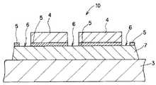
(第1の実施の形態)
図1に示すように、第1の実施の形態におけるカラーフィルタ基板10は、基板3と、基板3上に設けられた実質的に光を遮る遮光層7と、遮光層7上に設けられた実質的に光を反射させる反射膜5と、反射膜5上に設けられた着色層4とを有し、反射膜5は開口部6を有し着色層4によって覆われている。
【0026】
なお、図1においては、隣接する着色層4の間に間隙が設けられた場合を示すが、互いに接触し連続して設けられたものであってもよい。また、開口部6は上方から俯瞰的に見た場合、各画素領域を囲っている状態になる。以下の実施の形態の場合においても同様である。
【0027】
このように、反射膜5は開口部6を有しているため、遮光層7が露出し、遮光層7のコントラスト向上機能を十全に発揮させることができる。
【0028】
このように構成することによって、外部からの光を反射膜5で反射し、この反射光による画像を表示することが可能であり(反射型表示が可能であり)、機能性に優れるとともに安価な反射型の装置用のカラーフィルタ基板として好適に用いられることができる。
【0029】
以下、さらに具体的に説明する。
【0030】
本発明に用いられる基板3としては特に制限はないが、例えば、ガラスや石英、プラスティック等の光透過性を有する板状部材を挙げることができる。本実施の形態においては、必ずしも光透過性を有する基板3を用いる必要はない。
【0031】
また、着色層4は、通常、R(赤)、G(緑)及びB(青)のそれぞれの着色層を、基板3上の着色層形成領域に、所定の配列、例えば、ストライプ配列、モザイク配列、デルタ配列等の形状に形成される(図10参照)。具体的には、着色層4は、所定の色の樹脂材料、例えば、R(赤色)の顔料を分散させたアクリル樹脂によって、例えば、スピンコート法やインクジェット法を用いて、かつ所定のパターニング手法(例えば、フォトリソグラフィ法)を用いて基板3上の着色層形成領域に形成される。この場合、個々の着色層形成領域の平面寸法は、例えば、30μmm×100μm程度に形成される。
【0032】
また、反射膜5は、外部からの入射光を反射させるための膜であり、例えば、反射性を有する材料からなる膜(例えば、アルミニウムや銀、もしくはこれらの合金、又はこれらのチタン、窒化チタン、モリブデン、タンタル等との積層膜)によって形成される。
【0033】
また、遮光層は、通常、画像のコントラストを向上させる機能(ブラックマスク等の遮光機能)を発揮させるために用いられるが、本発明における遮光層7は、さらに反射型表示のための散乱機能をも兼ね備えている。
【0034】
遮光層7は、例えば、実質的に光を遮ることができる樹脂から形成されるが、このような遮光性樹脂としては、例えば、黒色の顔料を分散させたエポキシ樹脂を挙げることができる。
【0035】
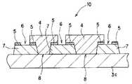
(第2の実施の形態)
図2に示すように、第2の実施の形態におけるカラーフィルタ基板10は、実質的に透明な基板3aと、この基板3a上に設けられた遮光層7と、遮光層7上に設けられた反射膜5と、基板3a上に設けられた着色層4とを有し、遮光層7は開口部8を有し、反射膜5は開口部6を有するとともに、着色層4によって覆われている。
【0036】
このように、遮光層7は開口部8を有しているため、バックライトユニットからの入射光は、この遮光層7の開口部8を通過するとともに着色層4を透過し、この透過光による画像を表示することも可能であり(透過型表示も可能であり)、反射膜5による反射型表示と相俟って、機能性に優れるとともに安価な半透過・半反射型の装置用のカラーフィルタ基板として好適に用いられることができる。従って、本実施の形態には実質的に透明な基板3aが用いられるが、その他の構成要素については、第1の実施の形態の場合と同様である。
【0037】
(第3の実施の形態)
図3に示すように、第3の実施の形態におけるカラーフィルタ基板10は、第2の実施の形態に用いられた基板3aに代えて、表面に凹凸を有する基板3bを用い、かつ遮光層7及び反射膜5として表面に凹凸を有する遮光層7a及び反射膜5aを用いたものである。すなわち、実質的に透明で表面に凹凸を有する基板3bと、この基板3b上に設けられた、基板3bの表面の凹凸形状に対応した表面凹凸形状を有する遮光層7aと、遮光層7a上に設けられた、遮光層7aの表面の凹凸形状に対応した表面凹凸形状を有する反射膜5aと、基板3bに設けられた着色層4とを有し、遮光層7aは開口部8を有し、反射膜5aは開口部6を有するとともに、着色層4によって覆われている。
【0038】
なお、図示はしないが、第2の実施の形態に用いられた基板、遮光層及び反射膜に代えて、第1の実施の形態に用いられた基板、遮光層及び反射膜を用い、これらの表面に凹凸を有するように構成したものであってもよい。
【0039】
このように構成することによって、基板3bの表面凹凸形状に対応して、表面に凹凸を有する遮光層7aを形成し、また、この遮光層7aの表面凹凸形状に対応して、表面に凹凸を有する反射膜5aを形成することができるため、表面に凹凸を有した遮光層7a及び反射膜5aを形成することが容易になる。このように、反射膜5aの表面に形成された凹凸形状によって、反射光を適度に散乱させることができるため、光学特性を向上させることができる。
【0040】
なお、図13に示すように、表面に凹凸を有する基板3bを用いずに、表面に凹凸を持たない基板3bを用いて、この基板3b上に、直接、表面に凹凸を有する遮光層7aを形成し、遮光層7aの表面凹凸形状に対応した形状の表面凹凸形状を有する反射膜5aを形成したものであってもよい。このように構成しても上述と同様の作用効果を得る事ができ、更には、基板表面に凹凸を形成するプロセスを省略することができ、工程を簡略化することができる。また、選択的に凹凸表面をもつ遮光層7aを形成することができるので、設計の自由度が高くなり、表面に凹凸を形成したくない領域には凹凸を形成しないようにする事も可能になる。
【0041】
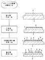
(第4の実施の形態)
図4に示すように、第4の実施の形態におけるカラーフィルタ基板の製造方法は、基板3上に、実質的に光を遮ることができる樹脂、例えば、黒色の顔料を分散させたエポキシ樹脂をスピンコート法によって塗布し、不要な部分を除去することによって遮光層7を形成する工程(遮光層形成工程)と、遮光層7上にスパッタリング等によって反射膜5を形成する工程(反射膜形成工程)と、フォトリソグラフィ技術及びエッチング技術を用いて反射膜5の開口部6を形成する工程(反射膜の開口部形成工程)と、反射膜5上に着色層4を形成する工程(着色層形成工程)とを含んでいる。
【0042】
このように構成することによって、機能性に優れた反射型の装置用のカラーフィルタ基板を効率よく、かつ低コストで製造することができる。
【0043】
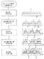
(第5の実施の形態)
図5に示すように、第5の実施の形態におけるカラーフィルタ基板の製造方法は、実質的に透明な基板3a上に実質的に光を遮ることができる樹脂、例えば、黒色の顔料を分散させたエポキシ樹脂をスピンコート法によって塗布し、不要な部分を除去することによって遮光層7を形成する工程と、フォトリソグラフィ技術を用いて遮光層7に開口部8を形成する工程(遮光層の開口部形成工程)と、遮光層7上にスパッタリング等によって反射膜5を形成する工程(反射膜形成工程)と、フォトリソグラフィ技術及びエッチング技術を用いて反射膜5の開口部6を形成する工程(反射膜の開口部形成工程)と、基板3a上に反射膜5を覆うようにして着色層を形成する工程(着色層形成工程)とを含んでいる。
【0044】
このように構成することによって、機能性に優れた半透過・半反射型の装置用のカラーフィルタ基板を効率よく、かつ低コストで製造することができる。
【0045】
(第6の実施の形態)
図6に示すように、第6の実施の形態は、第5の実施の形態におけるカラーフィルタ基板の製造方法に、後述する表面凹凸基板形成工程を加えたものである。すなわち、第6の実施の形態は、エッチング技術を用いて、実質的に透明な基板3aの表面に凹凸を形成し、表面に凹凸を有する基板3bを形成する工程(表面凹凸基板形成工程)と、表面に凹凸を有する基板3b上に実質的に光を遮ることができる樹脂、例えば、黒色の顔料を分散させたエポキシ樹脂をスピンコート法によって塗布し、不要な部分を除去することによって基板3bの表面凹凸形状に対応した形状を有する遮光層7aを形成する工程と、フォトリソグラフィ技術を用いて遮光層7aに、開口部8を形成する工程(遮光層の開口部形成工程)と、遮光層7a上に遮光層7aの表面凹凸形状に対応した形状を有する反射膜5aをスパッタリング等によって形成する工程(反射膜形成工程)と、フォトリソグラフィ技術及びエッチング技術を用いて反射膜5aの開口部6を形成する工程(反射膜の開口部形成工程)と、基板3b上に反射膜5aを覆うようにして着色層4を形成する工程(着色層形成工程)とを含んでいる。
【0046】
この場合、表面凹凸基板形成工程は省略してもよい。すなわち、図14に示すように、表面に凹凸を有しない基板3b上に、直接、フォトリソグラフィ技術及びエッチング技術を用いて表面に凹凸を有する遮光層7aを形成し、形成された遮光層7a上に遮光層7aの表面凹凸形状に対応した形状を有する反射膜5aを形成してもよい。このように構成しても上述と同様の作用効果を得る事ができ、更には、基板表面に凹凸を形成するプロセスを省略することができ、工程を簡略化することができる。また、選択的に凹凸表面をもつ遮光層7aを形成することができるので、設計の自由度が高くなり、表面に凹凸を形成したくない領域には凹凸を形成しないようにする事も可能になる。
【0047】
このように構成することによって、さらに機能性に優れた半透過・半反射型の装置用のカラーフィルタ基板を効率よく、かつ低コストで製造することができる。
【0048】
なお、図示はしないが、第4の実施の形態におけるカラーフィルタ基板の製造方法に、前述の表面凹凸基板形成工程を加えたものであってもよい。すなわち、表面凹凸基板形成工程において、第4の実施の形態で用いられた基板を用いてその表面に凹凸を形成するとともに、第4の実施の形態で用いられた遮光層及び反射膜の表面に凹凸を形成するものであってもよい。
【0049】
反射膜形成工程についての詳細は、本発明の電気光学装置の実施の形態のところで具体的に説明する。
【0050】
(第7の実施の形態)
図7に示すように、第7の実施の形態における電気光学装置(アクティブマトリックス方式の半透過反射型液晶表示装置として構成した場合であって、スイッチング素子として二端子型スイッチング素子を用いた場合を示す)は、一対の基板11,12と、一対の基板11,12のうち一方の基板12上に設けられた実質的に光を遮る遮光層107と、遮光層107上に設けられた実質的に光を反射する反射膜105と、反射膜105上に設けられた着色層104とを有し、反射膜105は開口部106を有することを特徴とする。なお、一方の基板12上に設けられた遮光層107、反射膜105及び着色層104は、図1〜図3に示すもののうちいずれの構成のものであってもよい。
【0051】
以下、さらに具体的に説明する。
図7に示すように、第7の実施の形態における電気光学装置は、シール材(図示せず)を介して対向する一対の基板(第1基板11及び第2基板12)の間に液晶13を挟持してなる液晶パネル1と、この液晶パネル1の第2基板(一方の基板)12側に配設されるバックライトユニット2とを含んで構成される。なお、実際には、第1基板11及び第2基板12の外側(液晶13とは反対側)の表面に、入射光を偏光させるための偏光板や位相差板等が貼着されるが、本発明とは直接関係がないため、その説明及び図示を省略する。
【0052】
バックライトユニット2は、光を照射する線状の蛍光管と、蛍光管から発せられる光を反射して導光板21に導く反射板と(いずれも図示せず)、蛍光管からの光を液晶パネル1の全面に導く導光板21と、この導光板21に導かれた光を液晶パネル1に対して一様に拡散させる拡散板22と、導光板21から液晶パネル1とは反対側に出射される光を液晶パネル1側へ反射させる反射板23とを有している。ここで、上記蛍光管は、常に点灯しているのではなく、外光がほとんどないような環境において使用される場合に、ユーザからの指示やセンサからの検出信号に応じて点灯し、これにより透過型表示が行われるようになっている。
【0053】
液晶パネル1の第1基板11は、ガラスや石英、プラスティック等の光透過性を有する板状部材である。この第1基板11の内側(液晶13側)表面には、複数の画素電極111がマトリックス状に配列して形成される。各画素電極111は、例えばITO(Indium Tin Oxide)等の透明導電材料によって形成される。
【0054】
図8は、画素電極111等が形成された第1基板11の表面を拡大して表す斜視図である。なお、図8と図7とでは、上下関係が逆になっている。
【0055】
図8に示すように、画素電極111は、TFD113を介して画素電圧供給用の走査線(図7においては紙面と垂直方向に延在して形成される)114に接続される。また、各TFD113は、走査線114から分岐した部分である第1金属膜113aと、この第1金属膜113aの表面に陽極酸化によって形成された絶縁体たる酸化膜113bと、この酸化膜113bの上面に例えばクロム等によって形成された第2金属膜113cとからなり、非線形な電流−電圧特性を有する二端子型スイッチング素子である。そして、このTFD113の第2金属膜113cが画素電極111に接続された構成となっている。
【0056】
図7において、画素電極111及びTFD113等が形成された第1基板11の表面は、配向膜112によって覆われている。この配向膜112は、ポリイミド等の有機薄膜であり、電圧が印加されていないときの液晶13の配向方向を規定するためのラビング処理が施されている。
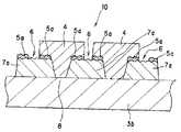
【0057】
一方、第2基板12は、ガラス基板等の基板12の表面上に形成した遮光性層107と、この遮光層107の表面上に形成した開口部106を有する反射膜105と、この反射膜105を覆うように形成されたカラーフィルタ(着色層)104とを積層して備えるように構成されている。さらに、オーバーコート層124と、対向電極125と、配向膜126とが形成されている。
【0058】
反射膜105は、前述のように、反射性を有する材料(例えばアルミニウムや銀等)によって形成され、第1基板11側からの入射光を反射させるための膜である。
【0059】
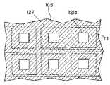
図9は、この反射膜105の形状を模式的に示す平面図である。なお、図9においては、反射膜105のうち、第1基板11に形成された画素電極111と対向する領域を破線で示している。図9に示すように、反射膜105は、第2基板12の全面を覆うように形成されるが、第2基板12の表面のうち、第1基板11に形成された各画素電極111と対向する領域の一部には開口部106が形成された形状となっている。後述するように、バックライトユニット2からの入射光は、この反射膜105の開口部106を通過して第1基板11側に出射し、透過型表示をする。
【0060】
ここで、第2基板12の内側表面(より詳細には、遮光層107の表面)のうち、反射膜105によって覆われる領域(以下、「反射領域」という)は、多数の微細な凹凸が形成された粗面となっている。このため、反射膜105の表面には、反射領域上の凹凸を反映した凹凸が形成されることとなる。
【0061】
カラーフィルタ(着色層)104は、上述のように、染料や顔料によってR(赤色)、G(緑色)及びB(青色)のいずれかに着色された樹脂材料で形成された膜である。また、反射膜105、遮光層107及びカラーフィルタ(着色層)104が形成された第2基板12の表面は、アクリル樹脂やエポキシ樹脂からなるオーバーコート層124によって覆われている。これは、遮光層107、反射膜105及びカラーフィルタ(着色層)104によって第2基板12上に形成された凸部を平坦化するとともに、カラーフィルタ(着色層)104から有機材料が染み出して液晶を劣化させるのを防止する。
【0062】
さらに、このオーバーコート層124の表面には、複数の対向電極125が形成されている。各対向電極125は、第1基板11上に列をなす複数の画素電極111の各々と対向するように所定の方向に延在して形成された帯状の電極であり、透明導電材料、例えば、ITO等によって形成される。第1基板11と第2基板12との間に挟持された液晶13は、画素電極111と対向電極125との間に電圧が印加されることによってその配向方向が変化する。すなわち、各画素電極111と各対向電極125とが対向する領域が画素として機能することとなる。
【0063】
上述した反射膜105の開口部106は、遮光性樹脂層12bが形成されない領域に対応して形成される。一方、これらの対向電極125が形成されたオーバーコート層124の表面は、上記配向膜112と同様の配向膜126によって覆われている。
【0064】
以上説明した構成により、以下に示す反射型表示及び透過型表示がなされることとなる。
【0065】
まず、反射型表示の場合、太陽光や室内照明等の外光は、第1基板11側から入射し、第1基板11、画素電極111、配向膜112、液晶13、配向膜126、対向電極125、オーバーコート層124、カラーフィルタ104、反射膜105という経路を順に辿り、反射膜105に達し、この反射膜105の表面で反射した後、上記経路を逆に辿って第1基板11側から出射して観察者に視認される。ここで、上述したように、反射膜105の表面には、第2基板12の反射領域に形成された凹凸を反映した凹凸が形成されている。このため、第1基板11側からの入射光は、この反射膜105の凹凸によって適度に散乱された後に第1基板11側から出射するから、観察者によって視認される画像に背景が映り込んだり、室内照明からの光が反射するといった事態を回避することができる。
【0066】
一方、透過型表示の場合、バックライトユニット2による照射光は、第2基板12、遮光層107の開口部8、反射膜121の開口部122、カラーフィルタ(着色層)123、オーバーコート層124、対向電極125、配向膜126、液晶13、配向膜112、画素電極111、第1基板11という経路を順に辿って出射して観察者に視認される。
【0067】
(第8の実施の形態)
第8の実施の形態における電気光学装置の製造方法は、基板上に実質的に光を遮る遮光層を形成する工程(遮光層形成工程)と、遮光層上に実質的に光を反射させる反射膜を形成する工程(反射膜形成工程)と、反射膜に開口部を形成する工程(反射膜の開口部形成工程)と、反射膜上に着色層を形成する工程(着色層形成工程)とを含んでいる。
【0068】
(第9の実施の形態)
第9の実施の形態における電気光学装置の製造方法は、実質的に透明な基板上に実質的に光を遮る遮光層を形成する工程(遮光層形成工程)と、遮光層に開口部を形成する工程(遮光層の開口部形成工程)と、遮光層上に反射膜を形成する工程(反射膜形成工程)と、反射膜に開口部を形成する工程(反射膜の開口部形成工程)と、基板上に反射膜を覆うように着色層を形成する工程(着色層形成工程)とを含んでいる。
【0069】
上記各工程は既に説明をしたので重複を避けるため、説明を割愛する。以下、上記各工程後の工程を、図7を参照しつつ説明する。
【0070】
上記各工程を経て形成された第2基板12の全面にアクリル樹脂等の樹脂材料を塗布し、その後焼成してオーバーコート層124を形成する。さらに、こうして形成されたオーバーコート層124の表面に、スパッタリング法等によってITOの薄膜を形成し、この薄膜に対してエッチングやフォトリソグラフィ等を施すことにより、複数の帯状の対向電極125を形成する。次に、これらの対向電極125が形成されたオーバーコート層124の表面にポリイミド等の有機材料を塗布・焼成して配向膜126を形成した後、この配向膜126に対して、用いる液晶13のツイスト角に応じた一軸配向処理(例えばラビング処理)を施す。
【0071】
一方、第1基板11の表面に、走査線114、TFD113及び画素電極111を形成する。これらの各部は、公知の各種方法を用いて形成することができる。
【0072】
次に、上記のようにして得られた第2基板12上に、この第2基板12の縁部を囲む形状のシール材を印刷するとともに、この第2基板12と、画素電極111等が形成された第1基板と11をシール材を介して接合し、液晶13を封入して液晶パネル1が得られる。この後、液晶パネル1の第2基板12側にバックライトユニット2を配設して、図7に示す電気光学装置が完成する。
【0073】
[変形例]
以上、本発明の電気光学装置の一実施の形態について説明したが、上記実施の形態はあくまでも例示であり、上記実施の形態に対しては、本発明の趣旨から逸脱しない範囲で様々な変形を加えることができる。変形例としては、例えば、以下のようなものが考えられる。
【0074】
<変形例1>
上記各実施の形態においては、二端子型スイッチング素子を用いたアクティブマトリックス方式の液晶表示装置を示したが、本発明は、例えば、TFT(Thin Film Transistor;薄膜トランジスタ)に代表される三端子型スイッチング素子を用いた液晶表示装置又はパッシブマトリックス方式の液晶表示装置にも適用可能である。これらの電気光学装置の場合も、上記各実施の形態におけると同様、液晶を挟持する一対の基板のうちの観察側とは反対側の基板に、遮光層、開口部を有する反射膜及びカラーフィルタ(着色層)を形成すればよい。また、上記各実施の形態においては、観察側の第1基板11に画素電極111及びTFD113等を設ける一方、観察側とは反対側の第2基板12に画素電極111と対向する対向電極125を設ける構成としたが、これとは逆に、第1基板11に対向電極を、第2基板12に画素電極及びスイッチング素子等を設ける構成としてもよい。一方、TFT等の三端子型スイッチング素子を用いた場合にあっても、観察側の基板をスイッチング素子が設けられた素子基板とし、他方の基板を対向電極が形成された対向基板としてもよいし、これとは逆に、観察側の基板を対向電極とし、観察側とは反対側の基板を素子基板としてもよい。また、本発明の電気光学装置は、液晶表示装置だけでなく、エレクトロルミネッセンス装置、有機エレクトロルミネッセンス装置、プラズマディスプレイ装置、電気泳動ディスプレイ装置、フィールド・エミッション・ディスプレイ(電界放出表示装置)などの各種の電気光学装置においても本発明を同様に適用することが可能である。
【0075】
<変形例2>
上記各実施の形態においては、第2基板12側に反射膜105と対向電極125とを別個に設ける構成としたが、反射膜105及び対向電極125の機能を兼ね備える反射電極を形成するようにしてもよい。
【0076】
【発明の効果】
以上説明したように、本発明によって、電気光学装置(特に、反射型液晶表示装置や半透過反射型液晶表示装置)に用いられた場合に、ブラックマスク等の遮光機能及び反射型表示のための散乱機能を簡易な構造で兼ね備え、機能性に優れるとともに安価なカラーフィルタ基板及びその製造方法、電気光学装置及びその製造方法並びに電子機器を提供することができる。
【図面の簡単な説明】
【図1】本発明のカラーフィルタ基板の実施の形態(第1の実施の形態)を模式的に示す断面図である。
【図2】本発明のカラーフィルタ基板の実施の形態(第2の実施の形態)を模式的に示す断面図である。
【図3】本発明のカラーフィルタ基板の実施の形態(第3の実施の形態)を模式的に示す断面図である。
【図4】本発明のカラーフィルタ基板及びその製造方法の実施の形態(第4の実施の形態)を工程順に模式的に示す断面図である。
【図5】本発明のカラーフィルタ基板及びその製造方法の実施の形態(第5の実施の形態)を工程順に模式的に示す断面図である。
【図6】本発明のカラーフィルタ基板及びその製造方法の実施の形態(第6の実施の形態)を工程順に模式的に示す断面図である。
【図7】本発明の電気光学装置の実施の形態(第7の実施の形態)を模式的に示す断面図である。
【図8】図7に示す電気光学装置の第1基板における画素電極近傍の構成を模式的に示す斜視図である。
【図9】図7に示す電気光学装置の反射膜の構成を模式的に示す平面図である。
【図10】カラーフィルタ(着色層)におけるR(赤)、G(緑)及びB(青)三色の絵素の配列例を示す平面図である。
【図11】従来の半透過・半反射型液晶表示装置の一例を模式的に示す断面図である。
【図12】従来の液晶表示装置に用いられる遮光層(ブラックマスクやブラックマトリックス)の一例を模式的に示す断面図である。
【図13】本発明のカラーフィルタ基板の実施の形態(第3の実施の形態)の変形例を模式的に示す断面図である。
【図14】本発明のカラーフィルタ基板及びその製造方法の実施の形態(第6の実施の形態)の変形例を工程順に模式的に示す断面図である。
【符号の説明】
1…液晶パネル
10…カラーフィルタ基板
11…第1基板
105…反射膜
106…開口部
107…カラーフィルタ(着色層)
111…画素電極
112…配向膜
113…TFD
114…走査線
12…第2基板
124…オーバーコート層
125…対向電極
126…配向膜
127…反射電極
127a…開口部
13…液晶
2…バックライトユニット
21…導光板
22…拡散板
23…反射板
3…基板
3a…実質的に透明な基板
3b…表面に凹凸を有する基板
4…着色層(カラーフィルタ)
5…反射膜
5a…表面に凹凸を有する反射膜
6…反射膜の開口部
7…遮光層
7a…表面に凹凸を有する樹脂層
8…遮光層の開口部[0001]
BACKGROUND OF THE INVENTION
The present invention relates to a color filter substrate, a manufacturing method thereof, an electro-optical device, a manufacturing method thereof, and an electronic apparatus. More specifically, when used in a liquid crystal display device (particularly a reflective liquid crystal display device or a transflective liquid crystal display device), the light shielding function such as a black mask and the scattering function for the reflective display have a simple structure. In addition, the present invention relates to a color filter substrate that is excellent in functionality and inexpensive and a method for manufacturing the same, a liquid crystal display device, a method for manufacturing the same, and an electronic device.
[0002]
[Prior art]
In recent years, liquid crystal display devices have been widely used in electronic devices such as mobile phones and portable personal computers. In addition, a liquid crystal display device having a structure for performing color display using a color filter substrate is also widely used.
[0003]
Conventionally, for example, R (red), G (green), and B (blue) colored layers are arranged in a predetermined arrangement, for example, a stripe arrangement, on the surface of a substrate conventionally formed of glass, plastic, or the like as a color filter substrate. What is formed in a mosaic arrangement, a delta arrangement, or the like is known (see FIG. 10).
[0004]
In addition, a reflection type display in which external light such as natural light or indoor illumination light is incident from the observation side and the light is reflected to perform display, and light from the light source is incident from the opposite side to display. A so-called transflective liquid crystal display device capable of switching between transmissive display as necessary is known.
[0005]
FIG. 11 is a cross-sectional view schematically showing an example of a conventional transflective liquid crystal display device, which is an active matrix type transflective liquid crystal having a TFD (Thin Film Diode) which is a two-terminal switching element. The structure of the display apparatus is shown typically.
[0006]
As shown in FIG. 11, the liquid crystal display device includes a
[0007]
As shown in FIG. 12, when performing color display in a conventional liquid crystal display device, a colored layer forming region is formed on the surface of a
[0008]
[Problems to be solved by the invention]
However, in the conventional liquid crystal display device, the
[0009]
The present invention has been made in view of the above-mentioned problems, and when used in a liquid crystal display device (particularly, a reflective liquid crystal display device or a transflective liquid crystal display device), An object of the present invention is to provide a color filter substrate and a manufacturing method thereof, a liquid crystal display device and a manufacturing method thereof, and an electronic apparatus which have a scattering function for a reflective display with a simple structure and are excellent in functionality and inexpensive.
[0010]
[Means for Solving the Problems]
In order to achieve the above object, the color filter substrate of the present invention comprises:A color filter substrate having a substrate and a plurality of pixels provided on the substrate, wherein each of the pixels is provided on a resin light shielding layer provided on the substrate and a part of an upper layer of the light shielding layer. A light-shielding layer that extends from the pixel so as to overlap a boundary region between adjacent pixels, and has an opening that transmits light into the pixel. The colored layer is provided in the opening and is thicker in the opening than the region overlapping with the reflective layer. In a cross-sectional view, the light shielding layer has a wide inclined surface toward the substrate. Is formed in the opening.
[0011]
Moreover, according to the color filter substrate which concerns on this invention, it is preferable that the uneven | corrugated shape is formed in the surface in which the light shielding layer of a board | substrate is provided.
Further, in each of the pixels, the reflective film has a slit for partitioning the colored layer and the colored layer of the adjacent pixel, and the light shielding layer exposed from the slit surrounds the pixel in plan view. preferable.
[0012]
By configuring as described above, when used in an electro-optical device (particularly, a reflective liquid crystal display device or a transflective liquid crystal display device), the light shielding function such as a black mask and the scattering for the reflective display are performed. It is possible to provide an inexpensive color filter substrate that has functions with a simple structure and is excellent in functionality.
[0013]
Further, the method of manufacturing the color filter substrate of the present invention includes a step of forming a light shielding layer that substantially blocks light on the substrate, a step of forming a reflective film that substantially reflects light on the light shielding layer, and Forming a colored layer on the reflective film, and in the step of forming the reflective film, an opening is preferably formed in the reflective film.
[0014]
The method for manufacturing a color filter substrate of the present invention includes a step of forming a light shielding layer that substantially blocks light on a substantially transparent substrate, and a reflective film that substantially reflects light on the light shielding layer. A step of forming a colored layer on the substrate, and in the step of forming the light shielding layer, in the step of forming an opening in the light shielding layer and forming the reflective film, the reflective film In the step of forming an opening in and forming the colored layer, the reflective film may be covered with the colored layer.
[0015]
By configuring as described above, the above-described color filter substrate can be manufactured efficiently and at low cost.
[0016]
In order to achieve the above object, a liquid crystal display device (electro-optical device) according to the present invention is a transflective liquid crystal display device having a display area for performing reflective display and transmissive display. The pixel comprises a plurality of pixels each having a reflective region for performing reflective display and a transmissive region for performing transmissive display. Each of the pixels includes a resin light-shielding layer provided on the substrate, and a light-shielding layer. A light-shielding layer that has a reflective film as a reflective region provided in a part of the upper layer and a colored layer that overlaps at least the reflective film, and extends so as to overlap a boundary region between adjacent pixels from within the pixel. The pixel has an opening that transmits light, and the colored layer is provided in the opening, and is thicker in the opening than the region overlapping the reflective layer. In the cross-sectional view, the light shielding layer faces the substrate. It has a wide inclined surface and the colored layer is Characterized in that it is formed in the opening.
[0017]
Further, according to the liquid crystal display device (electro-optical device) according to the present invention, it is preferable that an uneven shape is formed on the surface of the substrate on which the light shielding layer is provided.
Further, in each of the pixels, the reflective film has a slit for partitioning the colored layer and the colored layer of the adjacent pixel, and the light shielding layer exposed from the slit surrounds the pixel in plan view. preferable.
[0018]
By configuring as described above, it is possible to provide an electro-optical device that is excellent in functionality and inexpensive.
[0019]
The method of manufacturing the electro-optical device of the present invention includes a step of forming a light shielding layer that substantially blocks light on a substrate, and a step of forming a reflective film that substantially reflects light on the light shielding layer; Forming a colored layer on the reflective film, and in the step of forming the reflective film, an opening is preferably formed in the reflective film.
[0020]
The method of manufacturing the electro-optical device according to the invention includes a step of forming a light shielding layer that substantially blocks light on a substantially transparent substrate, and a reflective film that substantially reflects light on the light shielding layer. A step of forming a colored layer on the substrate, and in the step of forming the light shielding layer, in the step of forming an opening in the light shielding layer and forming the reflective film, the reflective film In the step of forming an opening in and forming the colored layer, the reflective film may be covered with the colored layer.
[0021]
By configuring as described above, an electro-optical device having excellent functionality can be efficiently manufactured at low cost.
[0022]
According to another aspect of the present invention, there is provided an electronic apparatus including the above-described electro-optical device.
[0023]
With such a configuration, it is possible to provide an electronic device that is excellent in functionality and inexpensive.
[0024]
DETAILED DESCRIPTION OF THE INVENTION
Hereinafter, embodiments of the present invention will be specifically described with reference to the drawings. Such embodiment shows one mode of the present invention, does not limit the present invention at all, and can be arbitrarily changed within the scope of the present invention.
[0025]
(First embodiment)
As shown in FIG. 1, the
[0026]
Although FIG. 1 shows a case where a gap is provided between adjacent
[0027]
Thus, since the
[0028]
With this configuration, it is possible to reflect light from the outside with the
[0029]
More specific description will be given below.
[0030]
Although there is no restriction | limiting in particular as the board |
[0031]
In addition, the
[0032]
The
[0033]
Further, the light shielding layer is usually used for exhibiting a function of improving the contrast of an image (light shielding function such as a black mask), but the
[0034]
The
[0035]
(Second Embodiment)
As shown in FIG. 2, the
[0036]
Thus, since the
[0037]
(Third embodiment)
As shown in FIG. 3, the
[0038]
Although not shown, instead of the substrate, the light shielding layer and the reflective film used in the second embodiment, the substrate, the light shielding layer and the reflective film used in the first embodiment are used. It may be configured to have irregularities on the surface.
[0039]
With this configuration, the light-shielding layer 7a having irregularities on the surface is formed corresponding to the surface irregularity shape of the
[0040]
As shown in FIG. 13, the light-shielding layer 7a having the surface irregularities is directly formed on the
[0041]
(Fourth embodiment)
As shown in FIG. 4, the method for manufacturing a color filter substrate in the fourth embodiment uses a resin that can substantially block light on the
[0042]
With such a configuration, a color filter substrate for a reflection type device having excellent functionality can be manufactured efficiently and at low cost.
[0043]
(Fifth embodiment)
As shown in FIG. 5, in the method of manufacturing the color filter substrate in the fifth embodiment, a resin that can substantially block light, for example, a black pigment, is dispersed on a substantially transparent substrate 3a. The step of forming the
[0044]
With this configuration, a color filter substrate for a semi-transmissive / semi-reflective device having excellent functionality can be manufactured efficiently and at low cost.
[0045]
(Sixth embodiment)
As shown in FIG. 6, the sixth embodiment is obtained by adding a surface uneven substrate forming step to be described later to the method for manufacturing a color filter substrate in the fifth embodiment. That is, in the sixth embodiment, an etching technique is used to form irregularities on the surface of a substantially transparent substrate 3a and to form a
[0046]
In this case, the surface uneven substrate forming step may be omitted. That is, as shown in FIG. 14, a light shielding layer 7a having irregularities on the surface is directly formed on the
[0047]
With such a configuration, a color filter substrate for a semi-transmissive / semi-reflective device having further excellent functionality can be manufactured efficiently and at low cost.
[0048]
Although not shown, the above-described surface uneven substrate forming step may be added to the method for manufacturing a color filter substrate in the fourth embodiment. That is, in the surface uneven substrate forming step, the substrate used in the fourth embodiment is used to form unevenness on the surface, and the surface of the light shielding layer and the reflective film used in the fourth embodiment is formed. Concavities and convexities may be formed.
[0049]
Details of the reflective film forming step will be specifically described in the embodiment of the electro-optical device of the invention.
[0050]
(Seventh embodiment)
As shown in FIG. 7, the electro-optical device according to the seventh embodiment (when configured as an active matrix transflective liquid crystal display device, using a two-terminal switching element as a switching element) 1), a pair of
[0051]
More specific description will be given below.
As shown in FIG. 7, the electro-optical device according to the seventh embodiment includes a
[0052]
The
[0053]
The
[0054]
FIG. 8 is an enlarged perspective view showing the surface of the
[0055]
As shown in FIG. 8, the
[0056]
In FIG. 7, the surface of the
[0057]
On the other hand, the
[0058]
As described above, the
[0059]
FIG. 9 is a plan view schematically showing the shape of the
[0060]
Here, in the inner surface of the second substrate 12 (more specifically, the surface of the light shielding layer 107), a region covered by the reflective film 105 (hereinafter referred to as “reflective region”) is formed with a large number of fine irregularities. It has become a rough surface. For this reason, unevenness reflecting the unevenness on the reflective region is formed on the surface of the
[0061]
As described above, the color filter (colored layer) 104 is a film formed of a resin material colored in one of R (red), G (green), and B (blue) with a dye or pigment. The surface of the
[0062]
Further, a plurality of
[0063]
The
[0064]
With the configuration described above, the following reflective display and transmissive display are performed.
[0065]
First, in the case of reflective display, external light such as sunlight or indoor illumination enters from the
[0066]
On the other hand, in the case of transmissive display, the light emitted from the
[0067]
(Eighth embodiment)
The electro-optical device manufacturing method according to the eighth embodiment includes a step of forming a light shielding layer that substantially blocks light on a substrate (a light shielding layer forming step), and a reflection that substantially reflects light on the light shielding layer. A step of forming a film (a reflective film forming step), a step of forming an opening in the reflective film (an opening of the reflective film), a step of forming a colored layer on the reflective film (a colored layer forming step), Is included.
[0068]
(Ninth embodiment)
The electro-optical device manufacturing method according to the ninth embodiment includes a step of forming a light shielding layer that substantially blocks light on a substantially transparent substrate (light shielding layer forming step), and an opening is formed in the light shielding layer. A step of forming an opening in the light shielding layer, a step of forming a reflective film on the light shielding layer (a reflective film forming step), a step of forming an opening in the reflective film (an opening of the reflective film), and And a step of forming a colored layer on the substrate so as to cover the reflective film (colored layer forming step).
[0069]
Since each said process has already been demonstrated, description is omitted in order to avoid duplication. Hereinafter, the steps after the above steps will be described with reference to FIG.
[0070]
A resin material such as acrylic resin is applied to the entire surface of the
[0071]
On the other hand, the
[0072]
Next, on the
[0073]
[Modification]
The electro-optical device according to the embodiment of the present invention has been described above. However, the above-described embodiment is merely an example, and various modifications can be made to the above-described embodiment without departing from the spirit of the present invention. Can be added. As modifications, for example, the following can be considered.
[0074]
<
In each of the above embodiments, an active matrix type liquid crystal display device using a two-terminal type switching element has been shown. However, the present invention is, for example, a three-terminal type switching represented by a TFT (Thin Film Transistor). The present invention can also be applied to a liquid crystal display device using an element or a passive matrix liquid crystal display device. Also in the case of these electro-optical devices, as in the above embodiments, a light-shielding layer, a reflective film having an opening, and a color filter are formed on the substrate opposite to the observation side of the pair of substrates that sandwich the liquid crystal. (Colored layer) may be formed. In each of the above embodiments, the
[0075]
<
In each of the above embodiments, the
[0076]
【The invention's effect】
As described above, according to the present invention, when used in an electro-optical device (particularly, a reflection type liquid crystal display device or a transflective type liquid crystal display device), a light shielding function such as a black mask and a reflection type display. It is possible to provide a color filter substrate that has a scattering function with a simple structure, is excellent in functionality, and is inexpensive, and a manufacturing method thereof, an electro-optical device, a manufacturing method thereof, and an electronic apparatus.
[Brief description of the drawings]
FIG. 1 is a cross-sectional view schematically showing an embodiment (first embodiment) of a color filter substrate of the present invention.
FIG. 2 is a cross-sectional view schematically showing an embodiment (second embodiment) of a color filter substrate of the present invention.
FIG. 3 is a cross-sectional view schematically showing an embodiment (third embodiment) of a color filter substrate of the present invention.
FIG. 4 is a cross-sectional view schematically showing an embodiment (fourth embodiment) of a color filter substrate and a manufacturing method thereof according to the present invention in the order of steps.
FIG. 5 is a cross-sectional view schematically showing an embodiment (fifth embodiment) of a color filter substrate and a manufacturing method thereof according to the present invention in the order of steps.
FIG. 6 is a cross-sectional view schematically showing an embodiment (sixth embodiment) of a color filter substrate and a manufacturing method thereof according to the present invention in the order of steps.
FIG. 7 is a cross-sectional view schematically showing an embodiment (seventh embodiment) of an electro-optical device according to the invention.
8 is a perspective view schematically showing a configuration in the vicinity of a pixel electrode on a first substrate of the electro-optical device shown in FIG.
9 is a plan view schematically showing a configuration of a reflective film of the electro-optical device shown in FIG.
FIG. 10 is a plan view showing an arrangement example of R (red), G (green), and B (blue) picture elements in a color filter (colored layer).
FIG. 11 is a cross-sectional view schematically showing an example of a conventional transflective / semi-reflective liquid crystal display device.
FIG. 12 is a cross-sectional view schematically showing an example of a light shielding layer (black mask or black matrix) used in a conventional liquid crystal display device.
FIG. 13 is a cross-sectional view schematically showing a modification of the embodiment (third embodiment) of the color filter substrate of the present invention.
FIG. 14 is a cross-sectional view schematically showing a modification of the embodiment (sixth embodiment) of the color filter substrate and the manufacturing method thereof according to the present invention in the order of steps.
[Explanation of symbols]
1 ... LCD panel
10 ... Color filter substrate
11 ... 1st board
105: Reflective film
106 ... opening
107 ... color filter (colored layer)
111 ... Pixel electrode
112 ... Alignment film
113 ... TFD
114 ... scan line
12 ... Second substrate
124 ... Overcoat layer
125 ... Counter electrode
126 ... Alignment film
127 ... Reflective electrode
127a ... opening
13 ... Liquid crystal
2 ... Backlight unit
21 ... Light guide plate
22 ... Diffusion plate
23 ... reflector
3 ... Board
3a: Substantially transparent substrate
3b... Substrate having irregularities on the surface
4. Colored layer (color filter)
5 ... Reflective film
5a ... Reflective film having irregularities on the surface
6 ... Opening of reflective film
7 ... Light shielding layer
7a ... Resin layer having irregularities on the surface
8: Opening of the light shielding layer
Claims (7)
Translated fromJapanese前記画素の各々は、Each of the pixels
前記基板上に設けられた樹脂製の遮光層と、A resin light-shielding layer provided on the substrate;
前記遮光層の上層の一部に設けられた反射膜と、A reflective film provided in a part of the upper layer of the light shielding layer;
少なくとも前記反射膜に重なる着色層と、を有し、A colored layer overlapping at least the reflective film,
前記画素内から隣り合う画素との境界領域に重なるように延在された前記遮光層は、前記画素内に光を透過する開口部を備え、The light-shielding layer extended so as to overlap a boundary region between adjacent pixels from within the pixel includes an opening that transmits light into the pixel,
前記着色層は、前記開口部に設けられるとともに、前記反射層と重なる領域よりも、前記開口部において厚く設けられ、The colored layer is provided in the opening, and is provided thicker in the opening than a region overlapping the reflective layer.
断面視において、前記遮光層は基板に向かって幅広の傾斜面を有し、In cross-sectional view, the light shielding layer has a wide inclined surface toward the substrate,
前記着色層は、前記開口部内に形成されていることを特徴とするカラーフィルタ基板。The color filter substrate, wherein the colored layer is formed in the opening.
平面視において、前記スリットから露出した前記遮光層が前記画素を囲っていることを特徴とする請求項1または2に記載のカラーフィルタ基板。In each of the pixels, the reflective film has a slit for partitioning the colored layer and a colored layer of the adjacent pixel,
The color filter substrate accordingto claim 1, wherein the light shielding layer exposed from the slit surrounds the pixel in a plan view .
前記表示領域は、それぞれが前記反射表示を行うための反射領域と、前記透過表示を行うための透過領域とを備えた、複数の画素からなり、The display area is composed of a plurality of pixels each including a reflective area for performing the reflective display and a transmissive area for performing the transmissive display,
前記画素の各々は、Each of the pixels
前記基板上に設けられた樹脂製の遮光層と、A resin light-shielding layer provided on the substrate;
前記遮光層の上層の一部に設けられた前記反射領域としての反射膜と、A reflective film as the reflective region provided in a part of the upper layer of the light shielding layer;
少なくとも前記反射膜に重なる着色層と、を有し、A colored layer overlapping at least the reflective film,
前記画素内から隣り合う画素との境界領域に重なるように延在された前記遮光層は、前記画素内に光を透過する開口部を備え、The light-shielding layer extended so as to overlap a boundary region between adjacent pixels from within the pixel includes an opening that transmits light into the pixel,
前記着色層は、前記開口部に設けられるとともに、前記反射層と重なる領域よりも、前記開口部において厚く設けられ、The colored layer is provided in the opening, and is provided thicker in the opening than a region overlapping the reflective layer.
断面視において、前記遮光層は基板に向かって幅広の傾斜面を有し、In cross-sectional view, the light shielding layer has a wide inclined surface toward the substrate,
前記着色層は、前記開口部内に形成されていることを特徴とする液晶表示装置。The liquid crystal display device, wherein the colored layer is formed in the opening.
平面視において、前記スリットから露出した前記遮光層が前記画素を囲っていることを特徴とする請求項4または5に記載の液晶表示装置。In each of the pixels, the reflective film has a slit for partitioning the colored layer and the colored layer of the adjacent pixel,
6. The liquid crystal display device according to claim 4, wherein the light shielding layer exposed from the slit surrounds the pixel in a plan view.
Priority Applications (1)
| Application Number | Priority Date | Filing Date | Title |
|---|---|---|---|
| JP2002195214AJP4045878B2 (en) | 2001-08-07 | 2002-07-03 | Color filter substrate, electro-optical device, and electronic apparatus |
Applications Claiming Priority (3)
| Application Number | Priority Date | Filing Date | Title |
|---|---|---|---|
| JP2001239608 | 2001-08-07 | ||
| JP2001-239608 | 2001-08-07 | ||
| JP2002195214AJP4045878B2 (en) | 2001-08-07 | 2002-07-03 | Color filter substrate, electro-optical device, and electronic apparatus |
Publications (3)
| Publication Number | Publication Date |
|---|---|
| JP2003121831A JP2003121831A (en) | 2003-04-23 |
| JP2003121831A5 JP2003121831A5 (en) | 2005-09-15 |
| JP4045878B2true JP4045878B2 (en) | 2008-02-13 |
Family
ID=26620128
Family Applications (1)
| Application Number | Title | Priority Date | Filing Date |
|---|---|---|---|
| JP2002195214AExpired - Fee RelatedJP4045878B2 (en) | 2001-08-07 | 2002-07-03 | Color filter substrate, electro-optical device, and electronic apparatus |
Country Status (1)
| Country | Link |
|---|---|
| JP (1) | JP4045878B2 (en) |
Families Citing this family (8)
| Publication number | Priority date | Publication date | Assignee | Title |
|---|---|---|---|---|
| JP3644442B2 (en) | 2001-08-07 | 2005-04-27 | セイコーエプソン株式会社 | Color filter substrate and manufacturing method thereof, liquid crystal display device and manufacturing method thereof, and electronic apparatus |
| JP3788448B2 (en) | 2003-07-18 | 2006-06-21 | セイコーエプソン株式会社 | Color filter substrate, transflective substrate, color filter substrate manufacturing method, electro-optical device, and electronic apparatus |
| JP2005062480A (en) | 2003-08-12 | 2005-03-10 | Seiko Epson Corp | COLOR FILTER, COLOR FILTER MANUFACTURING METHOD, DISPLAY DEVICE, ELECTRO-OPTICAL DEVICE, AND ELECTRONIC DEVICE |
| JP2005189429A (en)* | 2003-12-25 | 2005-07-14 | Casio Comput Co Ltd | Liquid crystal display element |
| JP4511248B2 (en)* | 2004-05-28 | 2010-07-28 | 京セラ株式会社 | Liquid crystal display |
| JP4337807B2 (en) | 2005-12-05 | 2009-09-30 | エプソンイメージングデバイス株式会社 | Liquid crystal device and electronic device |
| JP2020129305A (en)* | 2019-02-08 | 2020-08-27 | 株式会社グルマンディーズ | Accessories for portable information terminals |
| US10948775B2 (en)* | 2019-03-08 | 2021-03-16 | Nichia Corporation | Light source device |
- 2002
- 2002-07-03JPJP2002195214Apatent/JP4045878B2/ennot_activeExpired - Fee Related
Also Published As
| Publication number | Publication date |
|---|---|
| JP2003121831A (en) | 2003-04-23 |
Similar Documents
| Publication | Publication Date | Title |
|---|---|---|
| US6690438B2 (en) | Liquid crystal display panel | |
| JP3644442B2 (en) | Color filter substrate and manufacturing method thereof, liquid crystal display device and manufacturing method thereof, and electronic apparatus | |
| JP3692445B2 (en) | Liquid crystal device and electronic device | |
| JP3675420B2 (en) | Liquid crystal display device and electronic device | |
| JP3941548B2 (en) | Liquid crystal display panel, liquid crystal display panel substrate and electronic device | |
| US20050099558A1 (en) | Liquid crystal device and electronic apparatus provided with the same | |
| JP4075802B2 (en) | Liquid crystal display | |
| JP2007017798A (en) | Liquid crystal display device | |
| JP4045878B2 (en) | Color filter substrate, electro-optical device, and electronic apparatus | |
| JP2003043239A (en) | Color filter substrate, manufacturing method thereof, and liquid crystal display device | |
| US7639326B2 (en) | Liquid crystal device and electronic apparatus | |
| JP4952158B2 (en) | Manufacturing method of liquid crystal device | |
| JP2003084290A (en) | Liquid crystal display | |
| JP5121488B2 (en) | Liquid crystal device and electronic device | |
| JP4952544B2 (en) | Liquid crystal display device and electronic device | |
| JP2006343615A (en) | Liquid crystal device and electronic apparatus | |
| JP4511248B2 (en) | Liquid crystal display | |
| JP4254092B2 (en) | Liquid crystal display panel and electronic equipment | |
| JP4375172B2 (en) | Electro-optical device and electronic apparatus | |
| JP5334012B2 (en) | Transflective liquid crystal display panel and electronic equipment | |
| JP4905242B2 (en) | Liquid crystal device and electronic device | |
| JP3617520B2 (en) | Liquid crystal device | |
| JP4617982B2 (en) | Electro-optical device and electronic apparatus | |
| JP4075903B2 (en) | Liquid crystal display panel, liquid crystal display panel substrate and electronic device | |
| JP4042758B2 (en) | Liquid crystal device and electronic device |
Legal Events
| Date | Code | Title | Description |
|---|---|---|---|
| A521 | Written amendment | Free format text:JAPANESE INTERMEDIATE CODE: A523 Effective date:20050405 | |
| A621 | Written request for application examination | Free format text:JAPANESE INTERMEDIATE CODE: A621 Effective date:20050405 | |
| A977 | Report on retrieval | Free format text:JAPANESE INTERMEDIATE CODE: A971007 Effective date:20070712 | |
| A131 | Notification of reasons for refusal | Free format text:JAPANESE INTERMEDIATE CODE: A131 Effective date:20070731 | |
| A521 | Written amendment | Free format text:JAPANESE INTERMEDIATE CODE: A523 Effective date:20071001 | |
| TRDD | Decision of grant or rejection written | ||
| A01 | Written decision to grant a patent or to grant a registration (utility model) | Free format text:JAPANESE INTERMEDIATE CODE: A01 Effective date:20071030 | |
| A61 | First payment of annual fees (during grant procedure) | Free format text:JAPANESE INTERMEDIATE CODE: A61 Effective date:20071112 | |
| FPAY | Renewal fee payment (event date is renewal date of database) | Free format text:PAYMENT UNTIL: 20101130 Year of fee payment:3 | |
| R150 | Certificate of patent or registration of utility model | Ref document number:4045878 Country of ref document:JP Free format text:JAPANESE INTERMEDIATE CODE: R150 Free format text:JAPANESE INTERMEDIATE CODE: R150 | |
| FPAY | Renewal fee payment (event date is renewal date of database) | Free format text:PAYMENT UNTIL: 20101130 Year of fee payment:3 | |
| FPAY | Renewal fee payment (event date is renewal date of database) | Free format text:PAYMENT UNTIL: 20111130 Year of fee payment:4 | |
| FPAY | Renewal fee payment (event date is renewal date of database) | Free format text:PAYMENT UNTIL: 20111130 Year of fee payment:4 | |
| FPAY | Renewal fee payment (event date is renewal date of database) | Free format text:PAYMENT UNTIL: 20121130 Year of fee payment:5 | |
| FPAY | Renewal fee payment (event date is renewal date of database) | Free format text:PAYMENT UNTIL: 20121130 Year of fee payment:5 | |
| FPAY | Renewal fee payment (event date is renewal date of database) | Free format text:PAYMENT UNTIL: 20131130 Year of fee payment:6 | |
| S531 | Written request for registration of change of domicile | Free format text:JAPANESE INTERMEDIATE CODE: R313531 | |
| R350 | Written notification of registration of transfer | Free format text:JAPANESE INTERMEDIATE CODE: R350 | |
| R250 | Receipt of annual fees | Free format text:JAPANESE INTERMEDIATE CODE: R250 | |
| R250 | Receipt of annual fees | Free format text:JAPANESE INTERMEDIATE CODE: R250 | |
| LAPS | Cancellation because of no payment of annual fees |