JP4045241B2 - Heat sink with improved cooling capacity and semiconductor device including the heat sink - Google Patents
Heat sink with improved cooling capacity and semiconductor device including the heat sinkDownload PDFInfo
- Publication number
- JP4045241B2 JP4045241B2JP2003560991AJP2003560991AJP4045241B2JP 4045241 B2JP4045241 B2JP 4045241B2JP 2003560991 AJP2003560991 AJP 2003560991AJP 2003560991 AJP2003560991 AJP 2003560991AJP 4045241 B2JP4045241 B2JP 4045241B2
- Authority
- JP
- Japan
- Prior art keywords
- heat
- semiconductor device
- base portion
- heat sink
- heat spreader
- Prior art date
- Legal status (The legal status is an assumption and is not a legal conclusion. Google has not performed a legal analysis and makes no representation as to the accuracy of the status listed.)
- Expired - Fee Related
Links
Images


Classifications
- H—ELECTRICITY
- H01—ELECTRIC ELEMENTS
- H01L—SEMICONDUCTOR DEVICES NOT COVERED BY CLASS H10
- H01L23/00—Details of semiconductor or other solid state devices
- H01L23/34—Arrangements for cooling, heating, ventilating or temperature compensation ; Temperature sensing arrangements
- H01L23/36—Selection of materials, or shaping, to facilitate cooling or heating, e.g. heatsinks
- H01L23/373—Cooling facilitated by selection of materials for the device or materials for thermal expansion adaptation, e.g. carbon
- H01L23/3736—Metallic materials
- H—ELECTRICITY
- H01—ELECTRIC ELEMENTS
- H01L—SEMICONDUCTOR DEVICES NOT COVERED BY CLASS H10
- H01L23/00—Details of semiconductor or other solid state devices
- H01L23/34—Arrangements for cooling, heating, ventilating or temperature compensation ; Temperature sensing arrangements
- H01L23/36—Selection of materials, or shaping, to facilitate cooling or heating, e.g. heatsinks
- H01L23/367—Cooling facilitated by shape of device
- H—ELECTRICITY
- H01—ELECTRIC ELEMENTS
- H01L—SEMICONDUCTOR DEVICES NOT COVERED BY CLASS H10
- H01L2924/00—Indexing scheme for arrangements or methods for connecting or disconnecting semiconductor or solid-state bodies as covered by H01L24/00
- H01L2924/0001—Technical content checked by a classifier
- H01L2924/0002—Not covered by any one of groups H01L24/00, H01L24/00 and H01L2224/00
Landscapes
- Engineering & Computer Science (AREA)
- Chemical & Material Sciences (AREA)
- Materials Engineering (AREA)
- Physics & Mathematics (AREA)
- Condensed Matter Physics & Semiconductors (AREA)
- General Physics & Mathematics (AREA)
- Computer Hardware Design (AREA)
- Microelectronics & Electronic Packaging (AREA)
- Power Engineering (AREA)
- Cooling Or The Like Of Semiconductors Or Solid State Devices (AREA)
Description
Translated fromJapanese【0001】
【発明の属する技術分野】
【0002】
本発明は、冷却能力を効率化したヒートシンク及び該ヒートシンクを具備する半導体装置に関するものである。
【従来の技術】
【0003】
近年、LSI等の半導体装置の小型化・薄型化に加え、LSIの発熱量の増加に対応するために、ヒートシンクを具備する半導体装置において、ヒートシンクの冷却能力をより高効率にしようとする要求が増大している。ヒートシンクは、通常、LSI等の発熱する半導体部品の放熱効果を発揮するため、複数の放熱フィンを並列状に配したベース部と、半導体部品の表面などに接合させるヒートスプレッダとを備える。このヒートスプレッダを銅等の熱伝導性のよい金属材料で構成して、稼動時に発熱するLSIからの熱をヒートスプレッダとベース部を介して放熱フィンに伝導させ、放熱フィンにおいて熱を拡散させる機能を有する。ヒートシンクは、このような冷却能力を発揮して、稼動時の高発熱で耐熱温度を超えるような温度上昇が半導体装置に発生するのを防止する働きをする。
【0004】
一方、半導体装置の高集積化・高速化に伴い、高発熱量のLSIが増加しており、このような半導体装置に対し、ヒートシンクの冷却能力をより効率化にするためには、ヒートシンクのサイズを大きくする必要がある。しかし、半導体装置の構成上、ヒートシンクのサイズには制約があるために、従来のヒートシンクにおいてはその形状を改善するだけでは、十分な冷却能力を満足させることが困難であった。そこで、より高発熱な半導体装置に対しても冷却能力を低下させることがなく、ヒートシンクのサイズを現状と同等のレベルに維持可能な、あるいは、現状よりも小型化、薄型化が可能なヒートシンク構造が求められている。
【0005】
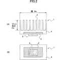
図1に、従来の埋め込み形ヒートシンクの一例を示す。図2は、図1に示した従来のヒートシンクを具備する半導体装置を示す。図2において、(A)は図1に示した一点鎖線II−IIに沿って切断した場合のこの半導体装置の断面図であり、(B)はこの半導体装置の裏面図である。
【0006】
図1、図2に示したように、従来のヒートシンク1は、複数の放熱フィン3を並列状に配したベース部4と、半導体装置5の表面に接合させたヒートスプレッダ2とを有する。半導体装置5は、LSI等の高発熱な半導体部品である。ベース部4は、例えば、アルミニウム等の金属材料で構成し、ヒートスプレッダ2を、ベース部4の構成材料より高い熱伝導率を有する、銅等の金属材料で構成している。この従来例では、所定の成形工程を実施することにより、銅製のヒートスプレッダ2がアルミニウム製ベース部4の裏面に埋め込まれ、互いに金属接合するよう形成される。
【発明が解決しようとする課題】
【0007】
図2に示したように、従来のヒートシンク1の場合、ヒートスプレッダ2の全表面がベース部4に接触する構成になっている。半導体装置5の表面は、接着または機械的接合によりヒートスプレッダ2に接合されている。稼動時に半導体装置5は発熱するが、半導体装置5からの熱をヒートスプレッダ2とベース部4を介して放熱フィン3に伝導させ、放熱フィン3において熱を拡散させている。しかし、半導体装置5とヒートスプレッダ2との境界面における接触熱抵抗、及びヒートスプレッダ2とベース部4との境界面における接触熱抵抗を小さくすることには限界があるため、従来のヒートシンクの場合、一定レベル以上の冷却能力を実現するは困難であった。
【0008】
さらに、高発熱なLSI等の半導体装置を冷却するためには、ある程度ベース部の厚さやヒートシンクのサイズ(特に、高さ)を大きくする必要がある。しかし、半導体装置に要求される条件により、許容できるヒートシンクのサイズには制約がある。そのため、従来のヒートシンクの場合には、ヒートシンクのサイズを現状と同等のレベルに維持しながら、より高発熱な半導体装置に対応して冷却能力を向上させることが困難であった。
本発明は、上記問題点に鑑みてなされたものであって、高発熱な半導体装置に対応できるよう冷却能力を効率化するとともに、薄型化、軽量化を可能にするヒートシンクを提供することを目的とする。
また、本発明の他の目的は、高発熱な半導体装置に対応できるよう冷却能力を効率化するとともに、薄型化、軽量化を可能にするヒートシンクを具備する半導体装置を提供することである。
【課題を解決するための手段】
【0009】
上記の課題を解決するために、本発明に係るヒートシンクは、半導体装置用のヒートシンクであって、複数の放熱フィンを第1の面に配設し、半導体装置と第2の面で直接に接触するベース部と、前記ベース部の第2の面に、前記半導体装置と直接に接触しないように配置したヒートスプレッダとを有し、前記ヒートスプレッダが、前記半導体装置の接触箇所の周縁を取り囲むように前記ベース部に埋め込まれるよう構成したことを特徴とする。
【0010】
また、上記のヒートシンクは、前記ヒートスプレッダが前記ベース部の構成材料よりも高い熱伝導率を有するように構成することができる。
【0011】
また、上記のヒートシンクは、前記ヒートスプレッダが前記半導体装置の接触箇所の周縁を取り囲むように複数個設けるように構成することができる。
【0012】
また、上記のヒートシンクは、前記ヒートスプレッダが前記ベース部の裏面と同一平面を有するように前記ベース部に埋め込まれるように構成することができる。
【0013】
また、上記の課題を解決するために、本発明に係るヒートシンクは、半導体装置用のヒートシンクであって、複数の放熱フィンを第1の面に配設し、半導体装置と第2の面で直接に接触するベース部と、前記ベース部の第2の面に、前記半導体装置と直接に接触しないように配置したヒートスプレッダとを有し、前記半導体装置の両側面に対向して、一対の前記ヒートスプレッダが前記ベース部に埋め込まれるとともに、各ヒートスプレッダが前記ベース部とほぼ同一の奥行きを有し、かつ、各ヒートスプレッダの側面にテーパ部を備えるよう構成することを特徴とする。
【0014】
さらに、上記の課題を解決するために、本発明に係るヒートシンクを具備する半導体装置は、前記ヒートシンクが、複数の放熱フィンを第1の面に配設し、前記半導体装置と第2の面で直接に接触するベース部と、前記ベース部の第2の面に、前記半導体装置と直接に接触しないように配置したヒートスプレッダとを有し、前記ヒートスプレッダが、前記半導体装置の接触箇所の周縁を取り囲むように前記ベース部に埋め込まれることを特徴とする。
【0015】
また、上記の半導体装置は、前記ヒートスプレッダが前記ベース部の構成材料よりも高い熱伝導率を有するように構成することができる。
【発明の効果】
【0016】
本発明のヒートシンクによれば、高発熱なLSI等の半導体装置に対する冷却性能を低下させることなく、放熱フィンの高さを小さくできるので、薄型化、軽量化を実現することができる。従来のヒートシンクと比較して、ヒートスプレッダとベース部との接触領域の熱伝導ロスを低減でき、ヒートシンクの放熱フィン全体に効率よく熱を拡散できるので、高発熱な半導体装置に対しても高い冷却性能を発揮することができる。
【発明の実施の形態】
【0017】
以下、本発明の実施の形態を添付図面を参照しながら具体的に説明する。尚、説明の都合上、従来例と基本的に同一の構成部分については同一の符号を付してその説明を省略するものとする。
【0018】
図3に、本発明に係るヒートシンクの基本的構成を示す。図4は、図3に示した本発明のヒートシンクを具備する半導体装置を説明するための図である。図4において、(A)は図3に示した一点鎖線IV−IVに沿って切断した場合の本発明に係る半導体装置の断面図であり、(B)は本発明に係る半導体装置の裏面図である。
【0019】
図3、図4に示したように、本発明に係るヒートシンク10は、ベース部4の表面に複数の放熱フィン3を並列状に配設すると共に、半導体装置5をベース部4の裏面に直接接合してある。ヒートスプレッダ20を、ベース部4の放熱フィン3と半導体装置5の間に介在させ、半導体装置5と直接に接触しないようにベース部4の裏面近傍に接合してある。
【0020】
半導体装置5は、例えば、LSI等の高発熱な半導体部品である。本発明に係るヒートシンク10においても、上述の従来例と同様に、ベース部4は、例えば、アルミニウム等の金属材料で構成し、ヒートスプレッダ20を、ベース部4の構成材料より高い熱伝導率を有する、銅等の金属材料で構成する。図4に示したヒートシンク10では、押し出し成形工程を実施することにより、銅製のヒートスプレッダ20がアルミニウム製ベース部4の裏面に埋め込まれ、互いに金属接合するよう形成される。
【0021】
図4に示したように、本発明に係るヒートシンク10においては、半導体装置5がベース部4の裏面に直接接合してあり、ヒートスプレッダ20に半導体装置5の周縁を取り囲む開口部20aを設ける等の方法により、ヒートスプレッダ20が半導体装置5と直接には接触せず、その周縁を取り囲むようにベース部4の裏面近傍に接合してある。従って、従来のヒートシンク1とは異なり、ヒートスプレッダとベース部裏面の中央部との境界面における接触熱抵抗が全く発生しない。
【0022】
本発明に係るヒートシンク10においては、稼動時に半導体装置5は発熱するが、半導体装置5からの熱は、ベース部4を介しベース部4表面の中央部に配設された放熱フィン3に伝わると共に、ベース部4裏面の中央部の境界面における接触熱抵抗が発生しないので、ベース部4表面の周辺部に配設された放熱フィン3にも、高熱伝導率を有する材料で構成されたヒートスプレッダ20とベース部4を介して伝わり易い。換言すれば、半導体装置5からの発熱量をベース部4表面の放熱フィン3全体に効率よく伝導させることができ、従来のヒートシンクと比較して、ヒートスプレッダ20とベース部4との接触領域の熱伝導ロスを低減できる。従って、より高発熱な半導体装置5に対しても、本発明に係るヒートシンク10は高い冷却能力を発揮することができる。
【0023】
従来のヒートシンクの冷却性能に対し本発明のヒートシンクの冷却性能がどの程度効率化できるかを説明するために、以下のようなシミュレーション解析を行って、比較、検討した例について詳述する。
【0024】
上記シミュレーション解析では、便宜上、半導体装置5は断面が正方形状で、大きさが31mmx31mmのLSIとし、この半導体装置を同一の発熱条件(10W)で稼動させた場合に、図2の従来のヒートシンク1の冷却性能(熱抵抗)と、図4のヒートシンク10の冷却性能(熱抵抗)とをそれぞれ求めることにより解析結果とした。
【0025】
両者に共通の解析条件として、ヒートシンクの周囲温度(Ta)は45℃、ヒートシンクを水平に設置し、フィン形状は大きさが90mmx90mmx60mmで、ベース部4の厚さが3mm、羽根枚数が30枚であり、ヒートスプレッダは大きさが66mmx66mmx2mmである。なお、図2と図4に示した構成ではヒートシンクの断面が長方形状であったが、ここでは、半導体装置5、従来のヒートシンク1及び本発明のヒートシンク10は全て、断面が正方形状であるとする。
【0026】
そして、上記シミュレーション解析では、従来のヒートシンク1の場合は、図2に示したように、 銅製のヒートスプレッダ2が全表面においてベース部4の裏面に埋め込まれた構成であり、半導体装置5(LSI)がヒートスプレッダ2の裏面に接合されているとする。この従来例の場合、ヒートシンクとLSIとの接合点におけるの温度(ジャンクション温度Tc)を上記発熱条件で求めた解析結果は約83.1℃であり、その冷却性能(熱抵抗)は約3.8℃/Wであった。
【0027】
これに対し、本発明のヒートシンク10の場合は、図4に示したように、半導体装置5(LSI)がベース4の裏面に直接接合してあり、銅製のヒートスプレッダ20には半導体装置5の周縁を取り囲む開口部20aが設けてあり、ヒートスプレッダ20が半導体装置5と直接には接触せずにベース部4の裏面に接合してあるとする。本発明に係るヒートシンク10の場合、ヒートシンクと半導体装置との接合点における温度(LSIジャンクション温度Tc)を上記発熱条件で求めた解析結果は約79.2℃であり、その冷却性能(熱抵抗)は約3.4℃/Wであった。すなわち、従来例と比較すると、本発明のヒートシンク10の場合、その冷却性能が約10%向上することが分かった。
【0028】
上述のように、高い冷却能力を発揮することができるので、本発明に係るヒートシンク10によれば、半導体装置の小型化、薄型化が要求される場合に、フィン高さを従来例のフィン高さ(図2に示したHo)より小さくできる。すなわち、本発明のヒートシンク10は、幅方向の長さをある程度拡大しても高い冷却能力を発揮できるので、そのフィン高さを従来例より小さくすることができ、したがって、半導体装置5に対する小型化、薄型化の要求を満足することができる。図4に示したように、本発明のヒートシンク10は、従来のヒートシンク1の幅(図2に示したWo)より大きな幅(図4に示したW)を有するベース部4を形成しても、高発熱なLSI等の半導体装置に対する冷却性能を低下させることがないので、従来例のフィン高さ(図2に示したHo)より小さいフィン高さ(図4に示したH)を有するヒートシンク10を構成することができる。したがって、半導体装置5に対する小型化、薄型化の要求を満足することができる。
【0029】
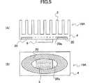
次に、図5は、本発明の第1実施例に係るヒートシンクを具備する半導体装置を示す。この実施例のヒートシンク10Aは、図4と同様に、ベース部4の表面に複数の放熱フィン3を並列状に配設し、半導体装置5をベース部4の裏面に直接接合してある。ヒートスプレッダ20を、ベース部4の放熱フィン3と半導体装置5の間に介在させ、半導体装置5と直接に接触しないようにベース部4の裏面近傍に接合してある。
【0030】
図5に示したように、この実施例のヒートスプレッダ20は、楕円形状に形成してあり、ベース部4の放熱フィン3全体に対応するよう十分大きな幅(長軸方向の長さ)を有する。また、半導体装置5の周縁を取り囲む楕円形状の開口部20aを有するよう構成してあり、このヒートスプレッダ20がベース部4の裏面と同一平面を有するようベース部4に埋め込まれている。
【0031】
この実施例のヒートシンク10Aは、ベース部4のヒートスプレッダ埋め込み用溝を形成する際に、押し出し加工もしくはダイカスト加工が行われる。押し出し加工で加工した場合には、後工程として、切削などの加工を行う必要がある。本実施例のヒートシンク10Aによれば、高発熱なLSI等の半導体装置に対する冷却性能を低下させることなく、放熱フィンの高さを小さくできるので薄型化、軽量化を実現できる。また、本実施例のヒートスプレッダ20により、ヒートシンクの放熱フィン全体に効率よく熱を拡散できるので、高発熱な半導体装置に対しても高い冷却性能を発揮できる。
【0032】
図6に、本発明の第2実施例に係るヒートシンクを具備する半導体装置を示す。この実施例のヒートシンク10Bは、図4と同様に、ベース部4の表面に複数の放熱フィン3を並列状に配設し、半導体装置5をベース部4の裏面に直接接合してある。ヒートスプレッダ20を、ベース部4の放熱フィン3と半導体装置5の間に介在させ、半導体装置5と直接に接触しないようにベース部4の裏面近傍に接合してある。
【0033】
図6に示したように、この実施例のヒートスプレッダ20は、矩形状に形成してあり、ベース部4の放熱フィン3全体に対応するよう十分大きな幅を有する。また、半導体装置5の周縁を取り囲む矩形状の開口部20aを有するよう構成してあり、このヒートスプレッダ20がベース部4の裏面と同一平面を有するようベース部4に埋め込まれている。
【0034】
この実施例のヒートシンク10Bは、ベース部4のヒートスプレッダ埋め込み用溝を形成する際に、押し出し加工もしくはダイカスト加工が行われる。押し出し加工で加工した場合には、後工程として、切削などの加工を行う必要がある。本実施例のヒートシンク10Bによれば、高発熱なLSI等の半導体装置に対する冷却性能を低下させることなく、放熱フィンの高さを小さくできるので薄型化、軽量化を実現できる。また、本実施例のヒートスプレッダ20により、ヒートシンクの放熱フィン全体に効率よく熱を拡散できるので、高発熱な半導体装置に対しても高い冷却性能を発揮できる。
【0035】
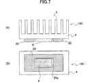
図7に、本発明の第3実施例に係るヒートシンクを具備する半導体装置を示す。この実施例のヒートシンク10Cは、図4と同様に、ベース部4の表面に複数の放熱フィン3を並列状に配設し、半導体装置5をベース部4の裏面に直接接合してある。ヒートスプレッダ20を、ベース部4の放熱フィン3と半導体装置5の間に介在させ、半導体装置5と直接に接触しないようにベース部4の裏面近傍に接合してある。
図7に示したように、この実施例のヒートシンク10Cは、貼り付け形のヒートシンクである。ヒートスプレッダ20の中央部には、半導体装置5の周縁を取り囲む開口部20aが設けてあり、このヒートスプレッダ20がベース部4の裏面に貼り付けた状態で接合されている。ヒートスプレッダ20は、開口部20aを設けているので、半導体装置5と直接に接触しないが、ベース部4の放熱フィン3全体に対応するように十分大きな幅を有するので、べース部4の放熱フィン3と半導体装置5の間に介在して、半導体装置5が発生する熱を放熱フィン3全体で効率よく拡散できる。
【0036】
この実施例のヒートシンク10Cによれば、高発熱なLSI等の半導体装置に対する冷却性能を低下させることなく、放熱フィンの高さを小さくできるので薄型化、軽量化を実現できる。また、本実施例のヒートスプレッダ20により、ヒートシンクの放熱フィン全体に効率よく熱を拡散できるので、高発熱な半導体装置に対しても高い冷却性能を発揮できる。
【0037】
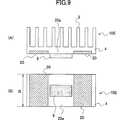
図8に、本発明の第4実施例に係るヒートシンクを具備する半導体装置を示す。この実施例のヒートシンク10Dは、図4と同様に、ベース部4の表面に複数の放熱フィン3を並列状に配設し、半導体装置5をベース部4の裏面に直接接合してある。ヒートスプレッダ20を、ベース部4の放熱フィン3と半導体装置5の間に介在させ、半導体装置5と直接に接触しないようにベース部4の裏面近傍に接合してある。
図8に示したように、この実施例のヒートスプレッダ20は、半導体装置5の周縁を取り囲むように4個設けてあり、これらのヒートスプレッダ20がベース部4の裏面と同一平面を有するようベース部4に埋め込まれている。4個のヒートスプレッダ20の間に挟まれた部分が、開口部20aとして設けられている。
【0038】
この実施例のヒートシンク10Dは、ベース部4のヒートスプレッダ埋め込み用溝を形成する際に、押し出し加工もしくはダイカスト加工が行われる。押し出し加工で加工した場合には、後工程として、切削などの加工を行う必要がある。本実施例のヒートシンク10Dによれば、高発熱なLSI等の半導体装置に対する冷却性能を低下させることなく、放熱フィンの高さを小さくできるので薄型化、軽量化を実現できる。また、本実施例のヒートスプレッダ20により、ヒートシンクの放熱フィン全体に効率よく熱を拡散できるので、高発熱な半導体装置に対しても高い冷却性能を発揮できる。
【0039】
図9に、本発明の第5実施例に係るヒートシンクを具備する半導体装置を示す。この実施例のヒートシンク10Eは、図4と同様に、ベース部4の表面に複数の放熱フィン3を並列状に配設し、半導体装置5をベース部4の裏面に直接接合してある。ヒートスプレッダ20を、ベース部4の放熱フィン3と半導体装置5の間に介在させ、半導体装置5と直接に接触しないようにベース部4の裏面近傍に接合してある。
図9に示したように、この実施例のヒートスプレッダ20は、半導体装置5の両側面に対向する一対のヒートスプレッダとして設けてあり、各ヒートスプレッダ20がベース部4に埋め込まれている。一対のヒートスプレッダ20の間に挟まれた部分が、開口部20aとして設けられている。各ヒートスプレッダ20は、ベース部4とほぼ同一の奥行きBを有するよう形成してある。
【0040】
この実施例のヒートシンク10Eの場合、ベース部4のヒートスプレッダ埋め込み用溝を形成する際には、押し出し加工のみで加工することが可能である。後工程で切削などの加工を行う必要がない。一方、従来の埋め込みタイプのヒートスプレッダを用いたヒートシンクの場合、ヒートスプレッダをベース部に埋め込んだ後、十分な平行度を得るために、切削などの後工程が必要であった。しかし、本実施例のヒートシンク10Eによれば、このような後工程が不要であり、したがって、製造コスト低減のために有用である。
【0041】
図10に、本発明の第6実施例に係るヒートシンクを具備する半導体装置を示す。この実施例のヒートシンク10Fは、図4と同様に、ベース部4の表面に複数の放熱フィン3を並列状に配設し、半導体装置5をベース部4の裏面に直接接合してある。ヒートスプレッダ20を、ベース部4の放熱フィン3と半導体装置5の間に介在させ、半導体装置5と直接に接触しないようにベース部4の裏面近傍に接合してある。
図10に示したように、この実施例のヒートスプレッダ20は、半導体装置5の両側面に対向する一対のヒートスプレッダとして設けてあり、各ヒートスプレッダ20がベース部4に埋め込まれている。一対のヒートスプレッダ20の間に挟まれた部分が、開口部20aとして設けられている。各ヒートスプレッダ20は、ベース部4とほぼ同一の奥行きBを有し、各ヒートスプレッダの両側面に、その幅が下方に減少するようなテーパ部を備えるよう形成してある。
【0042】
この実施例のヒートシンク10Fの場合も、ベース部4のヒートスプレッダ埋め込み用溝を形成する際には、押し出し加工のみで加工することが可能である。後工程で切削などの加工が不要である。さらに、この実施例の場合、各ヒートスプレッダ20の両側面にその幅が下方に減少するようなテーパ部を設けているので、各ヒートスプレッダ20をベース部4の埋め込み用溝に埋め込んだ後は、特別な接合を行わなくともベース部4から抜けにくい。したがって、本実施例のヒートシンク10Fは、製造コスト低減のためにさらに有用である。
尚、本発明は、上記実施例にのみ限定されるものではなく、本発明の趣旨を逸脱しない限り種々の改変を為すことができる。
【図面の簡単な説明】
【図1】従来のヒートシンクの構成を示す斜視図である。
【図2】図1に示した従来のヒートシンクを具備する半導体装置を説明するための図である。
【図3】本発明に係るヒートシンクの構成を示す斜視図である。
【図4】図3に示した本発明のヒートシンクを具備する半導体装置を説明するための図である。
【図5】本発明の第1実施例に係るヒートシンクを具備する半導体装置を説明するための図である。
【図6】本発明の第2実施例に係るヒートシンクを具備する半導体装置を説明するための図である。
【図7】本発明の第3実施例に係るヒートシンクを具備する半導体装置を説明するための図である。
【図8】本発明の第4実施例に係るヒートシンクを具備する半導体装置を説明するための図である。
【図9】本発明の第5実施例に係るヒートシンクを具備する半導体装置を説明するための図である。
【図10】本発明の第6実施例に係るヒートシンクを具備する半導体装置を説明するための図である。
【符号の説明】
1、10 ヒートシンク
2、20 ヒートスプレッダ
3 放熱フィン
4 ベース部[0001]
BACKGROUND OF THE INVENTION
[0002]
The present invention relates to a heat sink with improved cooling capacity and a semiconductor device including the heat sink.
[Prior art]
[0003]
In recent years, in addition to miniaturization and thinning of semiconductor devices such as LSIs, in order to cope with an increase in the amount of heat generated by LSIs, there has been a demand for higher efficiency in cooling capacity of heat sinks in semiconductor devices equipped with heat sinks. It is increasing. The heat sink usually includes a base portion in which a plurality of heat radiating fins are arranged in parallel and a heat spreader that is joined to the surface of the semiconductor component in order to exert a heat radiating effect of a semiconductor component that generates heat, such as an LSI. This heat spreader is made of a metal material having good thermal conductivity such as copper, and has the function of conducting heat from the LSI that generates heat during operation to the radiation fins through the heat spreader and the base, and diffusing heat in the radiation fins. . The heat sink exhibits such a cooling capability and functions to prevent the semiconductor device from generating a temperature rise that exceeds the heat-resistant temperature due to high heat generation during operation.
[0004]
On the other hand, with higher integration and higher speed of semiconductor devices, LSIs with higher heat generation are increasing. In order to make the heat sink cooling capacity more efficient for such semiconductor devices, the size of the heat sink Need to be larger. However, since the size of the heat sink is limited due to the configuration of the semiconductor device, it is difficult to satisfy the sufficient cooling capacity by simply improving the shape of the conventional heat sink. Therefore, a heat sink structure that can maintain the size of the heat sink at a level equivalent to the current level without reducing the cooling capacity even for semiconductor devices with higher heat generation, or that can be made smaller and thinner than the current level. Is required.
[0005]
FIG. 1 shows an example of a conventional embedded heat sink. FIG. 2 shows a semiconductor device having the conventional heat sink shown in FIG. 2A is a cross-sectional view of the semiconductor device when cut along the one-dot chain line II-II shown in FIG. 1, and FIG. 2B is a back view of the semiconductor device.
[0006]
As shown in FIGS. 1 and 2, the conventional heat sink 1 includes a base portion 4 in which a plurality of
[Problems to be solved by the invention]
[0007]
As shown in FIG. 2, in the case of the conventional heat sink 1, the entire surface of the
[0008]
Furthermore, in order to cool a semiconductor device such as a high heat generation LSI, it is necessary to increase the thickness of the base part and the size (particularly, the height) of the heat sink to some extent. However, the allowable heat sink size is limited depending on the conditions required for the semiconductor device. Therefore, in the case of the conventional heat sink, it is difficult to improve the cooling capacity corresponding to the semiconductor device with higher heat generation while maintaining the size of the heat sink at the same level as the current state.
The present invention has been made in view of the above problems, and an object of the present invention is to provide a heat sink that can improve the cooling capacity so as to be compatible with a highly heat-generating semiconductor device, and can be made thinner and lighter. And
Another object of the present invention is to provide a semiconductor device provided with a heat sink that makes it possible to reduce the thickness and weight while improving the efficiency of cooling so as to be compatible with a semiconductor device that generates high heat.
[Means for Solving the Problems]
[0009]
In order to solve the above problem, a heat sink according to the present invention,thereis provided a heat sink for a semiconductor device, arranged a plurality of heat radiation fins on the first surface, direct contact with the semiconductor device and the second surface a base portion which, in the second surface of the base portion,have a heat spreader arranged so as not to contact the semiconductor device anddirectly, the heat spreader, wherein so as to surround the periphery of the contact portion of the semiconductor device It is configured tobe embedded in the base portion .
[0010]
The heat sinkmay be configured such that the heat spreader has ahigher thermal conductivity than the constituent material of the base portion.
[0011]
Further, the heat sinkcan be the heat spreaderis configured to a plurality arrangedso that so as to surround the peripheryof the contact portion of the semiconductor device.
[0012]
The heat sink may be configured to be embedded in the base portion so that the heat spreader is flush with the back surface of the base portion.
[0013]
Inorder to solve the above-described problem, a heat sink accordingto the present invention is a heat sink for asemiconductor device, and a plurality of heat radiating fins are arranged on the first surface, and directly on the semiconductor device and the second surface. A pair of the heat spreaders facing the both side surfaces of the semiconductor device,the base portion contacting the semiconductor device, and a heat spreader disposed on the second surface of the base portion so as not to directly contact the semiconductor device. There together is embedded in the base portion, the heat spreader has substantially the same depth and the base portion, and,characterized by configured to include a tapered portion on a side surface of each heat spreader.
[0014]
Furthermore,in order to solve the above-described problems, in a semiconductor device including a heat sink according to the present invention, the heat sinkincludes a plurality of radiating fins disposed on a first surface, and the semiconductor device and the second surface. a base portion in direct contact, the second surface of the base portion,have a heat spreader arranged so as not to contact the semiconductor device anddirectly, the heat spreader, surrounds the periphery of the contact portion of the semiconductor device As described above, it isembedded in the base portion .
[0015]
The semiconductor device can be configured such that the heat spreader has a higher thermal conductivity than the constituent material of the base portion.
【The invention's effect】
[0016]
According to the heat sink of the present invention, the height of the radiating fin can be reduced without degrading the cooling performance for a semiconductor device such as LSI with high heat generation, and thus it is possible to reduce the thickness and weight. Compared to conventional heat sinks, heat conduction loss in the contact area between the heat spreader and the base can be reduced, and heat can be efficiently diffused throughout the heat sink fins, resulting in high cooling performance even for high heat generation semiconductor devices Can be demonstrated.
DETAILED DESCRIPTION OF THE INVENTION
[0017]
Hereinafter, embodiments of the present invention will be specifically described with reference to the accompanying drawings. For convenience of explanation, the same reference numerals are given to the same components as those in the conventional example, and the description thereof is omitted.
[0018]
FIG. 3 shows a basic configuration of the heat sink according to the present invention. FIG. 4 is a view for explaining a semiconductor device including the heat sink of the present invention shown in FIG. 4A is a cross-sectional view of the semiconductor device according to the present invention when cut along the alternate long and short dash line IV-IV shown in FIG. 3, and FIG. 4B is a back view of the semiconductor device according to the present invention. It is.
[0019]
As shown in FIGS. 3 and 4, the
[0020]
The
[0021]
As shown in FIG. 4, in the
[0022]
In the
[0023]
In order to explain how efficient the cooling performance of the heat sink of the present invention can be compared with the cooling performance of the conventional heat sink, the following simulation analysis is performed, and examples of comparison and examination will be described in detail.
[0024]
In the simulation analysis, for convenience, the
[0025]
As common analysis conditions for both, the heat sink ambient temperature (Ta) is 45 ° C., the heat sink is installed horizontally, the fin shape is 90 mm × 90 mm × 60 mm, the base part 4 is 3 mm thick, and the number of blades is 30 Yes, the heat spreader is 66 mm × 66 mm × 2 mm in size. 2 and FIG. 4, the cross section of the heat sink is rectangular. However, here, the
[0026]
In the simulation analysis, in the case of the conventional heat sink 1, as shown in FIG. 2, the
[0027]
On the other hand, in the case of the
[0028]
As described above, since a high cooling capacity can be exhibited, according to the
[0029]
Next, FIG. 5 shows a semiconductor device having a heat sink according to the first embodiment of the present invention. As in FIG. 4, the
[0030]
As shown in FIG. 5, the
[0031]
The
[0032]
FIG. 6 shows a semiconductor device having a heat sink according to a second embodiment of the present invention. As in FIG. 4, the
[0033]
As shown in FIG. 6, the
[0034]
The heat sink 10B of this embodiment is subjected to extrusion processing or die casting processing when the heat spreader embedding groove of the base portion 4 is formed. When processed by extrusion processing, it is necessary to perform processing such as cutting as a subsequent process. According to the heat sink 10B of the present embodiment, it is possible to reduce the height of the radiation fin without reducing the cooling performance for a semiconductor device such as a high heat generation LSI, so that the thickness and weight can be reduced. In addition, since the
[0035]
FIG. 7 shows a semiconductor device having a heat sink according to a third embodiment of the present invention. As in FIG. 4, the
As shown in FIG. 7, the heat sink 10C of this embodiment is an affixed heat sink. An
[0036]
According to the heat sink 10C of this embodiment, the height of the radiating fin can be reduced without lowering the cooling performance of a semiconductor device such as a high heat generation LSI, so that the thickness and weight can be reduced. In addition, since the
[0037]
FIG. 8 shows a semiconductor device having a heat sink according to a fourth embodiment of the present invention. As in FIG. 4, the
As shown in FIG. 8, four
[0038]
The heat sink 10D of this embodiment is subjected to extrusion processing or die casting processing when the heat spreader embedding groove of the base portion 4 is formed. When processed by extrusion processing, it is necessary to perform processing such as cutting as a subsequent process. According to the heat sink 10D of the present embodiment, the height of the heat radiation fin can be reduced without degrading the cooling performance of a semiconductor device such as a high heat generation LSI, so that it is possible to reduce the thickness and weight. In addition, since the
[0039]
FIG. 9 shows a semiconductor device having a heat sink according to a fifth embodiment of the present invention. In the
As shown in FIG. 9, the
[0040]
In the case of the
[0041]
FIG. 10 shows a semiconductor device having a heat sink according to a sixth embodiment of the present invention. In the
As shown in FIG. 10, the
[0042]
Also in the case of the
It should be noted that the present invention is not limited to the above embodiments, and various modifications can be made without departing from the spirit of the present invention.
[Brief description of the drawings]
FIG. 1 is a perspective view showing a configuration of a conventional heat sink.
2 is a diagram for explaining a semiconductor device including the conventional heat sink shown in FIG. 1; FIG.
FIG. 3 is a perspective view showing a configuration of a heat sink according to the present invention.
4 is a diagram for explaining a semiconductor device including the heat sink of the present invention shown in FIG. 3;
FIG. 5 is a diagram for explaining a semiconductor device including a heat sink according to a first embodiment of the present invention.
FIG. 6 is a diagram for explaining a semiconductor device including a heat sink according to a second embodiment of the present invention.
FIG. 7 is a view for explaining a semiconductor device including a heat sink according to a third embodiment of the present invention.
FIG. 8 is a diagram for explaining a semiconductor device including a heat sink according to a fourth embodiment of the present invention.
FIG. 9 is a view for explaining a semiconductor device including a heat sink according to a fifth embodiment of the present invention.
FIG. 10 is a diagram for explaining a semiconductor device including a heat sink according to a sixth embodiment of the present invention.
[Explanation of symbols]
1, 10 heat sink
2, 20 Heat spreader
3 Radiation fins
4 Base part
Claims (7)
Translated fromJapanese複数の放熱フィンを第1の面に配設し、半導体装置と第2の面で直接に接触するベース部と、
前記ベース部の第2の面に、前記半導体装置と直接に接触しないように配置したヒートスプレッダとを有し、前記ヒートスプレッダは、前記半導体装置の接触箇所の周縁を取り囲むように前記ベース部に埋め込まれることを特徴とするヒートシンク。In heat sinks for semiconductor devices,
A plurality of heat dissipating fins disposed on the first surface, and a base portion in direct contact with the semiconductor device on the second surface;
The second surface of the base portion,have a heat spreader arranged so as not to contact the semiconductor device anddirectly, the heat spreader is embedded in the base portion so as to surround the periphery of the contact portion of the semiconductor device A heat sink characterized by that.
複数の放熱フィンを第1の面に配設し、半導体装置と第2の面で直接に接触するベース部と、
前記ベース部の第2の面に、前記半導体装置と直接に接触しないように配置したヒートスプレッダとを有し、
前記半導体装置の両側面に対向して、一対の前記ヒートスプレッダが前記ベース部に埋め込まれるとともに、各ヒートスプレッダは、前記ベース部とほぼ同一の奥行きを有し、かつ、各ヒートスプレッダの側面にテーパ部を備えるよう構成することを特徴とするヒートシンク。In heat sinks for semiconductor devices,
A plurality of heat dissipating fins disposed on the first surface, and a base portion in direct contact with the semiconductor device on the second surface;
A heat spreader disposed on the second surface of the base portion so as not to directly contact the semiconductor device;
A pair of heat spreaders are embedded in the base portion so as to face both side surfaces of the semiconductor device, each heat spreader has substantially the same depth as the base portion, and a tapered portion is formed on the side surface of each heat spreader. A heat sink characterized by comprising a heat sink.
前記ヒートシンクは、
複数の放熱フィンを第1の面に配設し、前記半導体装置と第2の面で直接に接触するベース部と、
前記ベース部の第2の面に、前記半導体装置と直接に接触しないように配置したヒートスプレッダと、
を有し、前記ヒートスプレッダは、前記半導体装置の接触箇所の周縁を取り囲むように前記ベース部に埋め込まれることを特徴とする半導体装置。In a semiconductor device comprising a heat sink,
The heat sink is
A plurality of heat dissipating fins disposed on a first surface, and a base portion in direct contact with the semiconductor device on a second surface;
A heat spreader disposed on the second surface of the base portion so as not to directly contact the semiconductor device;
And theheat spreader is embedded in the base portion so as to surround a periphery of a contact portion of the semiconductor device.
Applications Claiming Priority (1)
| Application Number | Priority Date | Filing Date | Title |
|---|---|---|---|
| PCT/JP2002/000243WO2003061001A1 (en) | 2002-01-16 | 2002-01-16 | Heat sink having high efficiency cooling capacity and semiconductor device comprising it |
Publications (2)
| Publication Number | Publication Date |
|---|---|
| JPWO2003061001A1 JPWO2003061001A1 (en) | 2005-05-19 |
| JP4045241B2true JP4045241B2 (en) | 2008-02-13 |
Family
ID=11738133
Family Applications (1)
| Application Number | Title | Priority Date | Filing Date |
|---|---|---|---|
| JP2003560991AExpired - Fee RelatedJP4045241B2 (en) | 2002-01-16 | 2002-01-16 | Heat sink with improved cooling capacity and semiconductor device including the heat sink |
Country Status (3)
| Country | Link |
|---|---|
| US (2) | US7219721B2 (en) |
| JP (1) | JP4045241B2 (en) |
| WO (1) | WO2003061001A1 (en) |
Families Citing this family (39)
| Publication number | Priority date | Publication date | Assignee | Title |
|---|---|---|---|---|
| US7385820B1 (en)* | 2006-11-30 | 2008-06-10 | Foxconn Technology Co., Ltd. | Heat dissipation module |
| US8235094B2 (en)* | 2007-07-31 | 2012-08-07 | Adc Telecommunications, Inc. | Apparatus for transferring heat in a fin of a heat sink |
| US8051896B2 (en)* | 2007-07-31 | 2011-11-08 | Adc Telecommunications, Inc. | Apparatus for spreading heat over a finned surface |
| US20090032218A1 (en)* | 2007-07-31 | 2009-02-05 | Adc Telecommunications, Inc. | Apparatus for transferring between two heat conducting surfaces |
| US7539019B2 (en)* | 2007-07-31 | 2009-05-26 | Adc Telecommunications, Inc. | Apparatus for transferring heat from a heat spreader |
| US7672134B2 (en)* | 2007-11-30 | 2010-03-02 | Adc Telecommunications, Inc. | Apparatus for directing heat to a heat spreader |
| US8347502B2 (en)* | 2007-12-28 | 2013-01-08 | Ge Intelligent Platforms, Inc. | Heat sink and method of forming a heatsink using a wedge-lock system |
| BE1017916A3 (en)* | 2007-12-31 | 2009-11-03 | Gebotech Bv | HEAT EXCHANGER. |
| JP5537777B2 (en)* | 2008-02-08 | 2014-07-02 | 日本モレックス株式会社 | Heat sink, cooling module and coolable electronic board |
| US20090308584A1 (en)* | 2008-06-12 | 2009-12-17 | Tai-Her Yang | Thermal conduction principle and device of the multi-layers structure with different thermal characteristics |
| US20100038065A1 (en)* | 2008-08-14 | 2010-02-18 | Tai-Her Yang | Thermal conducting principle and device for prestressed clamping type multi-layered structure |
| US20100038066A1 (en)* | 2008-08-14 | 2010-02-18 | Tai-Her Yang | Thermal conducting principle and device for prestressed clamping type multi-layered structure |
| DE102009033063A1 (en)* | 2009-07-03 | 2010-09-23 | Siemens Aktiengesellschaft | Heat sink for cooling insulated gate bipolar transistor of e.g. converter, has heat dissipation devices formed from material e.g. copper, with heat conductance value that is higher than heat conductance value of material of base |
| US9179578B2 (en)* | 2009-08-25 | 2015-11-03 | Fuji Electric Co., Ltd. | Semiconductor module and heat radiation member |
| DE102009042519A1 (en)* | 2009-09-16 | 2011-03-24 | Esw Gmbh | Device for cooling semiconductors |
| JP5276565B2 (en)* | 2009-10-14 | 2013-08-28 | 新光電気工業株式会社 | Heat dissipation parts |
| US20110100606A1 (en)* | 2009-11-02 | 2011-05-05 | Beijing AVC Technology Research Center Co., Ltd. | Heat dissipating cavity |
| US7957148B1 (en) | 2009-12-08 | 2011-06-07 | International Business Machines Corporation | Low profile computer processor retention device |
| WO2011113178A1 (en)* | 2010-03-18 | 2011-09-22 | Telefonaktiebolaget L M Ericsson (Publ) | Cooling assembly for cooling heat generating component |
| TW201135429A (en)* | 2010-04-07 | 2011-10-16 | Hon Hai Prec Ind Co Ltd | Heat sink |
| KR20120000282A (en)* | 2010-06-25 | 2012-01-02 | 삼성전자주식회사 | Heat spreader and semiconductor package including the same |
| US20120061065A1 (en)* | 2010-09-15 | 2012-03-15 | Lacombe Ross M | Heat-absorbing structural material |
| DE102010048529B4 (en)* | 2010-10-14 | 2016-04-28 | Rohde & Schwarz Gmbh & Co. Kg | Heat sink with heat distributor |
| ITVI20100298A1 (en)* | 2010-11-09 | 2012-05-10 | Cbf Engineering S R L | HEATSINK |
| US20120261095A1 (en)* | 2011-04-12 | 2012-10-18 | Asia Vital Components Co., Ltd. | Thermal module structure and manufacturing method thereof |
| JP6132228B2 (en)* | 2012-02-15 | 2017-05-24 | パナソニックIpマネジメント株式会社 | Clothing with cooling or heating function |
| JP2015032758A (en)* | 2013-08-05 | 2015-02-16 | 日本発條株式会社 | Heat sink, power module and method of manufacturing heat sink |
| US9651236B2 (en)* | 2014-01-31 | 2017-05-16 | Christie Digital Systems Usa, Inc. | Light emitting device with a heat sink composed of two materials |
| US20150257249A1 (en)* | 2014-03-08 | 2015-09-10 | Gerald Ho Kim | Heat Sink With Protrusions On Multiple Sides Thereof And Apparatus Using The Same |
| JP6380027B2 (en)* | 2014-11-13 | 2018-08-29 | 株式会社デンソー | Electronic equipment |
| JP6458699B2 (en)* | 2015-09-30 | 2019-01-30 | 三菱マテリアル株式会社 | Discharge resistance device with cooler |
| WO2017086912A1 (en)* | 2015-11-16 | 2017-05-26 | Intel Corporation | Heat spreaders with interlocked inserts |
| JP6734594B2 (en)* | 2016-07-01 | 2020-08-05 | かがつう株式会社 | Heat sink, method for manufacturing the heat sink, and electronic component package using the heat sink |
| JP6763546B2 (en)* | 2018-02-07 | 2020-09-30 | Necプラットフォームズ株式会社 | Heat sink and how to assemble the heat sink |
| US11410905B2 (en) | 2019-03-18 | 2022-08-09 | International Business Machines Corporation | Optimized weight heat spreader for an electronic package |
| EP3933913A1 (en)* | 2020-06-30 | 2022-01-05 | Siemens Aktiengesellschaft | Power module with at least two power units |
| EP3961698A1 (en)* | 2020-08-26 | 2022-03-02 | Siemens Aktiengesellschaft | Semiconductor module with a cooling body |
| TWI785778B (en)* | 2021-09-06 | 2022-12-01 | 可成科技股份有限公司 | Heat dissipation mechanism and manufacturing method thereof |
| US20220225542A1 (en)* | 2022-02-25 | 2022-07-14 | Intel Corporation | Thin form factor assemblies for cooling dimms |
Family Cites Families (21)
| Publication number | Priority date | Publication date | Assignee | Title |
|---|---|---|---|---|
| US5459352A (en) | 1993-03-31 | 1995-10-17 | Unisys Corporation | Integrated circuit package having a liquid metal-aluminum/copper joint |
| US5367193A (en)* | 1993-06-17 | 1994-11-22 | Sun Microsystems, Inc. | Low cost, thermally efficient, and surface mountable semiconductor package for a high applied power VLSI die |
| JPH07273256A (en) | 1994-04-01 | 1995-10-20 | Nippon Steel Corp | Semiconductor device and heat spreader for the device |
| GB2293487B (en)* | 1994-09-21 | 1998-08-12 | Hewlett Packard Co | Method and apparatus for attaching a heat sink and a fan to an intergrated circuit package |
| JPH098188A (en) | 1995-06-15 | 1997-01-10 | Sumitomo Metal Mining Co Ltd | Heat spreader |
| US5981085A (en)* | 1996-03-21 | 1999-11-09 | The Furukawa Electric Co., Inc. | Composite substrate for heat-generating semiconductor device and semiconductor apparatus using the same |
| JPH09293808A (en) | 1996-04-25 | 1997-11-11 | Fujitsu Ltd | Semiconductor device |
| JP2845833B2 (en)* | 1996-09-12 | 1999-01-13 | 新潟日本電気株式会社 | heatsink |
| US6245442B1 (en)* | 1997-05-28 | 2001-06-12 | Kabushiki Kaisha Toyota Chuo | Metal matrix composite casting and manufacturing method thereof |
| US5969949A (en)* | 1998-03-31 | 1999-10-19 | Sun Microsystems, Inc. | Interfitting heat sink and heat spreader slug |
| JPH11317479A (en) | 1998-05-06 | 1999-11-16 | Sumitomo Metal Mining Co Ltd | Heat spreader member and composite heat spreader using the same |
| US6114048A (en)* | 1998-09-04 | 2000-09-05 | Brush Wellman, Inc. | Functionally graded metal substrates and process for making same |
| JP3881488B2 (en) | 1999-12-13 | 2007-02-14 | 株式会社東芝 | Circuit module cooling device and electronic apparatus having the cooling device |
| EP1187199A2 (en)* | 2000-08-28 | 2002-03-13 | Alcan Technology & Management AG | Heatsink for Semiconductor Device, Method of Mannufacturing the same, as well as Molding Die therefore |
| US20030051867A1 (en)* | 2001-09-19 | 2003-03-20 | Kennedy Paul S. | High heat flux heat sink and method of creating same |
| US6758263B2 (en)* | 2001-12-13 | 2004-07-06 | Advanced Energy Technology Inc. | Heat dissipating component using high conducting inserts |
| JP2004111665A (en)* | 2002-09-19 | 2004-04-08 | Hitachi Ltd | Electronic equipment |
| US6702007B1 (en)* | 2003-04-30 | 2004-03-09 | Kuan-Da Pan | Heat sink structure |
| US6977814B2 (en)* | 2003-05-06 | 2005-12-20 | Tyco Electronics Corporation | Dual material heat sink core assembly |
| US6898084B2 (en)* | 2003-07-17 | 2005-05-24 | The Bergquist Company | Thermal diffusion apparatus |
| US6849941B1 (en)* | 2004-01-07 | 2005-02-01 | Thermagon, Inc. | Heat sink and heat spreader assembly |
- 2002
- 2002-01-16JPJP2003560991Apatent/JP4045241B2/ennot_activeExpired - Fee Related
- 2002-01-16USUS10/500,464patent/US7219721B2/ennot_activeExpired - Fee Related
- 2002-01-16WOPCT/JP2002/000243patent/WO2003061001A1/ennot_activeCeased
- 2007
- 2007-01-03USUS11/648,632patent/US7431072B2/ennot_activeExpired - Fee Related
Also Published As
| Publication number | Publication date |
|---|---|
| US20070107872A1 (en) | 2007-05-17 |
| US7431072B2 (en) | 2008-10-07 |
| JPWO2003061001A1 (en) | 2005-05-19 |
| US20050006054A1 (en) | 2005-01-13 |
| US7219721B2 (en) | 2007-05-22 |
| WO2003061001A1 (en) | 2003-07-24 |
Similar Documents
| Publication | Publication Date | Title |
|---|---|---|
| JP4045241B2 (en) | Heat sink with improved cooling capacity and semiconductor device including the heat sink | |
| JP4979768B2 (en) | Thermally conductive composite interface, cooling electronic assembly using the same, and method for coupling cooling assembly and heat generating electronic device | |
| KR200448519Y1 (en) | Heat Sink for Protruding IC Packages | |
| EP1117130A2 (en) | Heatsink method of manufacturing the same and cooling apparatus using the same | |
| EP1995774A2 (en) | Semiconductor device | |
| JP5851599B2 (en) | Power module | |
| JP6421549B2 (en) | Power module | |
| JP2001217363A (en) | Semiconductor device and its heat sink | |
| JP2002289750A (en) | Multi-chip module and its radiation structure | |
| JPH10335521A (en) | Semiconductor device | |
| US11735557B2 (en) | Power module of double-faced cooling | |
| TW200401601A (en) | Cooling element for an electronic device | |
| JP5092274B2 (en) | Semiconductor device | |
| JP2008124187A (en) | Base for power module | |
| JP2008124187A6 (en) | Power module base | |
| JP2022171153A (en) | semiconductor module | |
| JP4460791B2 (en) | Heat sink for semiconductor devices | |
| JP5047422B2 (en) | Heat absorber | |
| JP2006210611A (en) | A heat sink provided with heat radiation fins and a method of manufacturing the same. | |
| CN214176014U (en) | Radiator of power element | |
| JP2000091481A (en) | Power transistor case and power transistor | |
| CN103135720B (en) | Radiating fin, radiator and manufacturing method of radiating fin | |
| JP2002043480A (en) | Semiconductor device | |
| CN113410191A (en) | Mounting structure of power semiconductor module | |
| JP2004031577A (en) | Heat sink for semiconductor devices |
Legal Events
| Date | Code | Title | Description |
|---|---|---|---|
| A131 | Notification of reasons for refusal | Free format text:JAPANESE INTERMEDIATE CODE: A131 Effective date:20070612 | |
| A521 | Request for written amendment filed | Free format text:JAPANESE INTERMEDIATE CODE: A523 Effective date:20070813 | |
| TRDD | Decision of grant or rejection written | ||
| A01 | Written decision to grant a patent or to grant a registration (utility model) | Free format text:JAPANESE INTERMEDIATE CODE: A01 Effective date:20071113 | |
| A61 | First payment of annual fees (during grant procedure) | Free format text:JAPANESE INTERMEDIATE CODE: A61 Effective date:20071119 | |
| R150 | Certificate of patent or registration of utility model | Free format text:JAPANESE INTERMEDIATE CODE: R150 | |
| FPAY | Renewal fee payment (event date is renewal date of database) | Free format text:PAYMENT UNTIL: 20101122 Year of fee payment:3 | |
| FPAY | Renewal fee payment (event date is renewal date of database) | Free format text:PAYMENT UNTIL: 20101122 Year of fee payment:3 | |
| FPAY | Renewal fee payment (event date is renewal date of database) | Free format text:PAYMENT UNTIL: 20111122 Year of fee payment:4 | |
| FPAY | Renewal fee payment (event date is renewal date of database) | Free format text:PAYMENT UNTIL: 20111122 Year of fee payment:4 | |
| FPAY | Renewal fee payment (event date is renewal date of database) | Free format text:PAYMENT UNTIL: 20121122 Year of fee payment:5 | |
| FPAY | Renewal fee payment (event date is renewal date of database) | Free format text:PAYMENT UNTIL: 20121122 Year of fee payment:5 | |
| FPAY | Renewal fee payment (event date is renewal date of database) | Free format text:PAYMENT UNTIL: 20131122 Year of fee payment:6 | |
| LAPS | Cancellation because of no payment of annual fees |