JP4044187B2 - Active matrix display device and manufacturing method thereof - Google Patents
Active matrix display device and manufacturing method thereofDownload PDFInfo
- Publication number
- JP4044187B2 JP4044187B2JP30651797AJP30651797AJP4044187B2JP 4044187 B2JP4044187 B2JP 4044187B2JP 30651797 AJP30651797 AJP 30651797AJP 30651797 AJP30651797 AJP 30651797AJP 4044187 B2JP4044187 B2JP 4044187B2
- Authority
- JP
- Japan
- Prior art keywords
- transistor
- electrode
- photoelectric conversion
- insulating film
- electrically connected
- Prior art date
- Legal status (The legal status is an assumption and is not a legal conclusion. Google has not performed a legal analysis and makes no representation as to the accuracy of the status listed.)
- Expired - Fee Related
Links
Images


Classifications
- H—ELECTRICITY
- H04—ELECTRIC COMMUNICATION TECHNIQUE
- H04N—PICTORIAL COMMUNICATION, e.g. TELEVISION
- H04N1/00—Scanning, transmission or reproduction of documents or the like, e.g. facsimile transmission; Details thereof
- H04N1/00127—Connection or combination of a still picture apparatus with another apparatus, e.g. for storage, processing or transmission of still picture signals or of information associated with a still picture
- H04N1/00129—Connection or combination of a still picture apparatus with another apparatus, e.g. for storage, processing or transmission of still picture signals or of information associated with a still picture with a display device, e.g. CRT or LCD monitor
- G—PHYSICS
- G02—OPTICS
- G02F—OPTICAL DEVICES OR ARRANGEMENTS FOR THE CONTROL OF LIGHT BY MODIFICATION OF THE OPTICAL PROPERTIES OF THE MEDIA OF THE ELEMENTS INVOLVED THEREIN; NON-LINEAR OPTICS; FREQUENCY-CHANGING OF LIGHT; OPTICAL LOGIC ELEMENTS; OPTICAL ANALOGUE/DIGITAL CONVERTERS
- G02F1/00—Devices or arrangements for the control of the intensity, colour, phase, polarisation or direction of light arriving from an independent light source, e.g. switching, gating or modulating; Non-linear optics
- G02F1/01—Devices or arrangements for the control of the intensity, colour, phase, polarisation or direction of light arriving from an independent light source, e.g. switching, gating or modulating; Non-linear optics for the control of the intensity, phase, polarisation or colour
- G02F1/13—Devices or arrangements for the control of the intensity, colour, phase, polarisation or direction of light arriving from an independent light source, e.g. switching, gating or modulating; Non-linear optics for the control of the intensity, phase, polarisation or colour based on liquid crystals, e.g. single liquid crystal display cells
- G02F1/133—Constructional arrangements; Operation of liquid crystal cells; Circuit arrangements
- G02F1/135—Liquid crystal cells structurally associated with a photoconducting or a ferro-electric layer, the properties of which can be optically or electrically varied
- G—PHYSICS
- G02—OPTICS
- G02F—OPTICAL DEVICES OR ARRANGEMENTS FOR THE CONTROL OF LIGHT BY MODIFICATION OF THE OPTICAL PROPERTIES OF THE MEDIA OF THE ELEMENTS INVOLVED THEREIN; NON-LINEAR OPTICS; FREQUENCY-CHANGING OF LIGHT; OPTICAL LOGIC ELEMENTS; OPTICAL ANALOGUE/DIGITAL CONVERTERS
- G02F1/00—Devices or arrangements for the control of the intensity, colour, phase, polarisation or direction of light arriving from an independent light source, e.g. switching, gating or modulating; Non-linear optics
- G02F1/01—Devices or arrangements for the control of the intensity, colour, phase, polarisation or direction of light arriving from an independent light source, e.g. switching, gating or modulating; Non-linear optics for the control of the intensity, phase, polarisation or colour
- G02F1/13—Devices or arrangements for the control of the intensity, colour, phase, polarisation or direction of light arriving from an independent light source, e.g. switching, gating or modulating; Non-linear optics for the control of the intensity, phase, polarisation or colour based on liquid crystals, e.g. single liquid crystal display cells
- G02F1/133—Constructional arrangements; Operation of liquid crystal cells; Circuit arrangements
- G02F1/136—Liquid crystal cells structurally associated with a semi-conducting layer or substrate, e.g. cells forming part of an integrated circuit
- G02F1/1362—Active matrix addressed cells
- G02F1/136227—Through-hole connection of the pixel electrode to the active element through an insulation layer
- G—PHYSICS
- G02—OPTICS
- G02F—OPTICAL DEVICES OR ARRANGEMENTS FOR THE CONTROL OF LIGHT BY MODIFICATION OF THE OPTICAL PROPERTIES OF THE MEDIA OF THE ELEMENTS INVOLVED THEREIN; NON-LINEAR OPTICS; FREQUENCY-CHANGING OF LIGHT; OPTICAL LOGIC ELEMENTS; OPTICAL ANALOGUE/DIGITAL CONVERTERS
- G02F1/00—Devices or arrangements for the control of the intensity, colour, phase, polarisation or direction of light arriving from an independent light source, e.g. switching, gating or modulating; Non-linear optics
- G02F1/01—Devices or arrangements for the control of the intensity, colour, phase, polarisation or direction of light arriving from an independent light source, e.g. switching, gating or modulating; Non-linear optics for the control of the intensity, phase, polarisation or colour
- G02F1/13—Devices or arrangements for the control of the intensity, colour, phase, polarisation or direction of light arriving from an independent light source, e.g. switching, gating or modulating; Non-linear optics for the control of the intensity, phase, polarisation or colour based on liquid crystals, e.g. single liquid crystal display cells
- G02F1/133—Constructional arrangements; Operation of liquid crystal cells; Circuit arrangements
- G02F1/136—Liquid crystal cells structurally associated with a semi-conducting layer or substrate, e.g. cells forming part of an integrated circuit
- G02F1/1362—Active matrix addressed cells
- G02F1/13624—Active matrix addressed cells having more than one switching element per pixel
- G—PHYSICS
- G02—OPTICS
- G02F—OPTICAL DEVICES OR ARRANGEMENTS FOR THE CONTROL OF LIGHT BY MODIFICATION OF THE OPTICAL PROPERTIES OF THE MEDIA OF THE ELEMENTS INVOLVED THEREIN; NON-LINEAR OPTICS; FREQUENCY-CHANGING OF LIGHT; OPTICAL LOGIC ELEMENTS; OPTICAL ANALOGUE/DIGITAL CONVERTERS
- G02F1/00—Devices or arrangements for the control of the intensity, colour, phase, polarisation or direction of light arriving from an independent light source, e.g. switching, gating or modulating; Non-linear optics
- G02F1/01—Devices or arrangements for the control of the intensity, colour, phase, polarisation or direction of light arriving from an independent light source, e.g. switching, gating or modulating; Non-linear optics for the control of the intensity, phase, polarisation or colour
- G02F1/13—Devices or arrangements for the control of the intensity, colour, phase, polarisation or direction of light arriving from an independent light source, e.g. switching, gating or modulating; Non-linear optics for the control of the intensity, phase, polarisation or colour based on liquid crystals, e.g. single liquid crystal display cells
- G02F1/133—Constructional arrangements; Operation of liquid crystal cells; Circuit arrangements
- G02F1/136—Liquid crystal cells structurally associated with a semi-conducting layer or substrate, e.g. cells forming part of an integrated circuit
- G02F1/1362—Active matrix addressed cells
- G02F1/136286—Wiring, e.g. gate line, drain line
- H—ELECTRICITY
- H04—ELECTRIC COMMUNICATION TECHNIQUE
- H04N—PICTORIAL COMMUNICATION, e.g. TELEVISION
- H04N1/00—Scanning, transmission or reproduction of documents or the like, e.g. facsimile transmission; Details thereof
- H04N1/00127—Connection or combination of a still picture apparatus with another apparatus, e.g. for storage, processing or transmission of still picture signals or of information associated with a still picture
- H—ELECTRICITY
- H04—ELECTRIC COMMUNICATION TECHNIQUE
- H04N—PICTORIAL COMMUNICATION, e.g. TELEVISION
- H04N1/00—Scanning, transmission or reproduction of documents or the like, e.g. facsimile transmission; Details thereof
- H04N1/024—Details of scanning heads ; Means for illuminating the original
- H04N1/028—Details of scanning heads ; Means for illuminating the original for picture information pick-up
- H04N1/02805—Details of scanning heads ; Means for illuminating the original for picture information pick-up with photodetectors arranged in a two-dimensional array
- H—ELECTRICITY
- H10—SEMICONDUCTOR DEVICES; ELECTRIC SOLID-STATE DEVICES NOT OTHERWISE PROVIDED FOR
- H10D—INORGANIC ELECTRIC SEMICONDUCTOR DEVICES
- H10D86/00—Integrated devices formed in or on insulating or conducting substrates, e.g. formed in silicon-on-insulator [SOI] substrates or on stainless steel or glass substrates
- H—ELECTRICITY
- H10—SEMICONDUCTOR DEVICES; ELECTRIC SOLID-STATE DEVICES NOT OTHERWISE PROVIDED FOR
- H10F—INORGANIC SEMICONDUCTOR DEVICES SENSITIVE TO INFRARED RADIATION, LIGHT, ELECTROMAGNETIC RADIATION OF SHORTER WAVELENGTH OR CORPUSCULAR RADIATION
- H10F39/00—Integrated devices, or assemblies of multiple devices, comprising at least one element covered by group H10F30/00, e.g. radiation detectors comprising photodiode arrays
- H10F39/10—Integrated devices
- H10F39/12—Image sensors
- H10F39/191—Photoconductor image sensors
- G—PHYSICS
- G02—OPTICS
- G02F—OPTICAL DEVICES OR ARRANGEMENTS FOR THE CONTROL OF LIGHT BY MODIFICATION OF THE OPTICAL PROPERTIES OF THE MEDIA OF THE ELEMENTS INVOLVED THEREIN; NON-LINEAR OPTICS; FREQUENCY-CHANGING OF LIGHT; OPTICAL LOGIC ELEMENTS; OPTICAL ANALOGUE/DIGITAL CONVERTERS
- G02F1/00—Devices or arrangements for the control of the intensity, colour, phase, polarisation or direction of light arriving from an independent light source, e.g. switching, gating or modulating; Non-linear optics
- G02F1/01—Devices or arrangements for the control of the intensity, colour, phase, polarisation or direction of light arriving from an independent light source, e.g. switching, gating or modulating; Non-linear optics for the control of the intensity, phase, polarisation or colour
- G02F1/13—Devices or arrangements for the control of the intensity, colour, phase, polarisation or direction of light arriving from an independent light source, e.g. switching, gating or modulating; Non-linear optics for the control of the intensity, phase, polarisation or colour based on liquid crystals, e.g. single liquid crystal display cells
- G02F1/133—Constructional arrangements; Operation of liquid crystal cells; Circuit arrangements
- G02F1/13306—Circuit arrangements or driving methods for the control of single liquid crystal cells
- G02F1/13312—Circuits comprising photodetectors for purposes other than feedback
- G—PHYSICS
- G02—OPTICS
- G02F—OPTICAL DEVICES OR ARRANGEMENTS FOR THE CONTROL OF LIGHT BY MODIFICATION OF THE OPTICAL PROPERTIES OF THE MEDIA OF THE ELEMENTS INVOLVED THEREIN; NON-LINEAR OPTICS; FREQUENCY-CHANGING OF LIGHT; OPTICAL LOGIC ELEMENTS; OPTICAL ANALOGUE/DIGITAL CONVERTERS
- G02F1/00—Devices or arrangements for the control of the intensity, colour, phase, polarisation or direction of light arriving from an independent light source, e.g. switching, gating or modulating; Non-linear optics
- G02F1/01—Devices or arrangements for the control of the intensity, colour, phase, polarisation or direction of light arriving from an independent light source, e.g. switching, gating or modulating; Non-linear optics for the control of the intensity, phase, polarisation or colour
- G02F1/13—Devices or arrangements for the control of the intensity, colour, phase, polarisation or direction of light arriving from an independent light source, e.g. switching, gating or modulating; Non-linear optics for the control of the intensity, phase, polarisation or colour based on liquid crystals, e.g. single liquid crystal display cells
- G02F1/133—Constructional arrangements; Operation of liquid crystal cells; Circuit arrangements
- G02F1/1333—Constructional arrangements; Manufacturing methods
- G02F1/133345—Insulating layers
- G—PHYSICS
- G02—OPTICS
- G02F—OPTICAL DEVICES OR ARRANGEMENTS FOR THE CONTROL OF LIGHT BY MODIFICATION OF THE OPTICAL PROPERTIES OF THE MEDIA OF THE ELEMENTS INVOLVED THEREIN; NON-LINEAR OPTICS; FREQUENCY-CHANGING OF LIGHT; OPTICAL LOGIC ELEMENTS; OPTICAL ANALOGUE/DIGITAL CONVERTERS
- G02F1/00—Devices or arrangements for the control of the intensity, colour, phase, polarisation or direction of light arriving from an independent light source, e.g. switching, gating or modulating; Non-linear optics
- G02F1/01—Devices or arrangements for the control of the intensity, colour, phase, polarisation or direction of light arriving from an independent light source, e.g. switching, gating or modulating; Non-linear optics for the control of the intensity, phase, polarisation or colour
- G02F1/13—Devices or arrangements for the control of the intensity, colour, phase, polarisation or direction of light arriving from an independent light source, e.g. switching, gating or modulating; Non-linear optics for the control of the intensity, phase, polarisation or colour based on liquid crystals, e.g. single liquid crystal display cells
- G02F1/133—Constructional arrangements; Operation of liquid crystal cells; Circuit arrangements
- G02F1/136—Liquid crystal cells structurally associated with a semi-conducting layer or substrate, e.g. cells forming part of an integrated circuit
- G02F1/1362—Active matrix addressed cells
- G02F1/136286—Wiring, e.g. gate line, drain line
- G02F1/13629—Multilayer wirings
- H—ELECTRICITY
- H04—ELECTRIC COMMUNICATION TECHNIQUE
- H04M—TELEPHONIC COMMUNICATION
- H04M1/00—Substation equipment, e.g. for use by subscribers
- H04M1/02—Constructional features of telephone sets
- H04M1/0202—Portable telephone sets, e.g. cordless phones, mobile phones or bar type handsets
- H04M1/026—Details of the structure or mounting of specific components
- H04M1/0264—Details of the structure or mounting of specific components for a camera module assembly
- H—ELECTRICITY
- H04—ELECTRIC COMMUNICATION TECHNIQUE
- H04M—TELEPHONIC COMMUNICATION
- H04M1/00—Substation equipment, e.g. for use by subscribers
- H04M1/02—Constructional features of telephone sets
- H04M1/0202—Portable telephone sets, e.g. cordless phones, mobile phones or bar type handsets
- H04M1/026—Details of the structure or mounting of specific components
- H04M1/0266—Details of the structure or mounting of specific components for a display module assembly
Landscapes
- Physics & Mathematics (AREA)
- Nonlinear Science (AREA)
- Engineering & Computer Science (AREA)
- Crystallography & Structural Chemistry (AREA)
- Mathematical Physics (AREA)
- Chemical & Material Sciences (AREA)
- Signal Processing (AREA)
- Multimedia (AREA)
- General Physics & Mathematics (AREA)
- Optics & Photonics (AREA)
- Microelectronics & Electronic Packaging (AREA)
- Liquid Crystal (AREA)
- Solid State Image Pick-Up Elements (AREA)
- Thin Film Transistor (AREA)
Description
Translated fromJapanese【0001】
【発明が属する技術分野】
本発明は、イメージセンサ機能と、表示機能を有する装置に関して、特に、マトリクス状に配置された複数の画素電極からなる画素部で構成された表示部を有するアクティブマトリクスパネルや、表示部を有する携帯端末機や、表示部を有するパソコン等の電子機器およびその作製方法に関するものである。
【0002】
【従来の技術】
近年、ポリシリコンTFTと呼ばれる多結晶シリコンを用いたTFT技術が鋭意研究されている。その成果として、ポリシリコンTFTによって、シフトレジスタ回路等の駆動回路を作製することが可能になり、画素部と、画素部を駆動する周辺駆動回路とを同一基板上に集積したアクティブマトリクス型の液晶パネルが実用化に至っている。そのため、液晶パネルが低コスト化、小型化、軽量化され、パーソナルコンピュータ、携帯電話、ビデオカメラやデジタルカメラ等の各種情報機器、携帯機器の表示部に用いられている。
【0003】
また、最近では、ノート型パソコンよりも携帯性に優れ、安価なポケットサイズの小型携帯用情報処理端末装置が実用化されており、その表示部にはアクティブマトリクス型液晶パネルが用いられている。このような情報処理端末装置は表示部からタッチペン方式でデータを入力可能となっているが、紙面上の文字・図画情報や、映像情報を入力するには、スキャナーやデジタルカメラ等の画像を読み込むための周辺機器と接続することが必要である。そのため、情報処理端末装置の携帯性が損なわれている。また、使用者に周辺機器を購入するための経済的な負担をかけている。
【0004】
また、アクティブマトリクス型表示装置は、TV会議システム、TV電話、インターネット用端末等の表示部にも用いられている。これらシステムや端末では、対話者や使用者の映像を撮影するカメラ(CCDカメラ)を備えているが、表示部と読み取り部(センサ部)は個別に製造されてモジュール化されている。そのため、製造コストが高いものとなっていた。
【0005】
【発明が解決しようとする課題】
本発明の目的は、上述した問題点を解消し、画素マトリクス、イメージセンサ、及びそれらを駆動するための周辺回路を有する、すなわち、撮像機能と表示機能とを兼ね備え、インテリジェント化された新規な半導体装置を用いた表示装置を提供することにある。
【0006】
更に本発明の目的は、イメージセンサを画素マトリクス、周辺駆動回路と構造・製造プロセスに整合性のあるものとすることにより、インテリジェント化された新規な半導体装置を用いた表示装置を安価に作製することにある。
【0007】
【課題を解決するための手段】
上記課題を解決するために、本発明は、同一基板上に表示用半導体装置と、受光用半導体装置とを設ける構成とした。そして、画素電極及び表示用半導体装置を含む液晶表示部と、受光用半導体装置を含むセンサ部とを別々に配置するのではなく、1つの画素内に表示用半導体装置と受光用半導体装置を有する新規な素子構成、すなわち、図1または図2に示すように、1つの画素内に表示と受光の両方の制御を行う半導体装置(絶縁ゲート型電界効果半導体装置)を有する構成とすることで、画像読み取り機能を有する表示装置を小型化、コンパクト化する。
【0008】
本明細書で開示する発明の第1の構成は、
少なくともマトリクス状に画素電極と、前記画素電極に接続された第1の半導体装置を有する画素マトリクスからなる表示部と、
少なくとも光電変換素子と、前記光電変換素子に接続された第2の半導体装置からなるセンサ部とが同一基板表面上に設けられ、
前記基板の裏面からの光を前記センサ部で受光することを特徴とするイメージセンサ機能を有する一体型液晶表示パネルである。
【0009】
また、本発明の第2の構成は、
少なくともマトリクス状に画素電極と、前記画素電極に接続された第1の半導体装置を有する画素マトリクスからなる表示部と、
少なくとも光電変換素子と、前記光電変換素子に接続された第2の半導体装置からなるセンサ部とが同一基板表面上に設けられ、
前記表示部と前記センサ部は同じ画素サイズを有し、
前記基板の裏面からの光を前記センサ部で受光することを特徴とするイメージセンサ機能を有する一体型液晶表示パネルである。
【0010】
また、本発明の第3の構成は、
少なくともマトリクス状に画素電極と、前記画素電極に接続された第1の半導体装置を有する画素マトリクスからなる表示部と、
少なくとも光電変換素子と、前記光電変換素子に接続された第2の半導体装置からなるセンサ部とが同一基板上に設けられ、
前記第1の半導体装置と前記第2の半導体装置は同一マトリクス内に設けられ、
前記第1の半導体装置に接続されている画素電極は、前記第2の半導体装置の上方に存在していることを特徴とするイメージセンサ機能を有する一体型液晶表示パネルである。
【0011】
また、本発明の第4の構成は、
少なくともマトリクス状に画素電極と、前記画素電極に接続された第1の半導体装置を有する画素マトリクスからなる表示部と、
少なくとも光電変換素子と、前記光電変換素子に接続された第2の半導体装置からなるセンサ部とが同一基板上に設けられ、
前記光電変換素子は、少なくとも上部電極と、光電変換層と、下部電極で構成され、
前記上部電極は、少なくとも可視光に対して反射性を有する金属からなり、
前記下部電極が透明性導電膜からなることを特徴とするイメージセンサ機能を有する一体型液晶表示パネルである。
【0012】
また、本発明の第5の構成は、
マトリクス状に配置された画素電極と、前記画素電極に接続された第1の半導体装置を有する画素マトリクスと、
光電変換素子と、前記光電変換素子に接続された第2の半導体装置とを有する受光部を有するイメージセンサと、が同一基板上に設けられたイメージセンサ機能を有する一体型液晶表示パネルの作製方法であって、
前記基板上に、前記第1の半導体装置と前記第2の半導体装置とを作製する第1の工程と、
前記第2の半導体装置と接続された透光性導電膜でなる下部電極を形成する第2の工程と、
前記下部電極上に光電変換層を形成する第3の工程と、
前記光電変換層上に接する上部電極を形成する第4の工程と、を少なくとも有するイメージセンサ機能を有する一体型液晶表示パネルの作製方法である。
【0013】
また、本発明の第6の構成は、
マトリクス状に配置された画素電極と、前記画素電極に接続された第1の半導体装置を有する画素マトリクスと、
光電変換素子と、前記光電変換素子に接続された第2の半導体装置とを有する受光部を有するイメージセンサと、が同一基板上に設けられたイメージセンサ機能を有する一体型液晶表示パネルの作製方法であって、
前記基板上に、前記第1の半導体装置と前記第2の半導体装置とを作製する第1の工程と、
前記第1の半導体装置と前記第2の半導体装置とを少なくとも覆う第1の絶縁膜を形成する第2の工程と、
前記第1の絶縁膜上に透光性導電膜を形成する第3の工程と、
前記透光性導電膜をパターニングして、前記第2の半導体装置と接続された下部電極を形成する第4の工程と、
前記下部電極上に光電変換層を形成する第5の工程と、
前記光電変換層上に接する上部電極を形成する第6の工程と、を少なくとも有するイメージセンサ機能を有する一体型液晶表示パネルの作製方法である。
【0014】
また、本発明の第7の構成は、
光電変換素子が、下部電極と、下部電極上に形成された光電変換層と、光電変換層上に形成された上部電極で構成され、
前記光電変換素子に接続された少なくとも1つのアクティブ素子からなるセンサ部とが絶縁基板上に設けられ、
前記上部電極は、少なくとも可視光に対して反射性を有する金属からなり、
前記下部電極が少なくとも可視光に対して透明性を有する導電膜からなることを特徴とするイメージセンサ機能を有する一体型液晶表示パネルである。
【0015】
また、本発明の第8の構成は、
少なくともマトリクス状に画素電極と、前記画素電極に接続されたアクティブ素子を有する画素マトリクスからなる表示部と、
少なくとも光電変換素子と、前記光電変換素子に接続されたアクティブ素子群からなるセンサ部とが同一基板表面上に設けられ、
前記基板の裏面からの光を前記センサ部で受光することを特徴とするイメージセンサ機能を有する一体型液晶表示パネルである。
【0016】
また、本発明の第9の構成は、
少なくともマトリクス状に画素電極と、前記画素電極に接続されたアクティブ素子を有する画素マトリクスからなる表示部と、
少なくとも光電変換素子と、前記光電変換素子に接続されたアクティブ素子群からなるセンサ部とが同一基板表面上に設けられ、
前記表示部と前記センサ部は同じ画素サイズを有し、
前記基板の裏面からの光を前記センサ部で受光することを特徴とするイメージセンサ機能を有する一体型液晶表示パネルである。
【0017】
また、本発明の第10の構成は、
少なくともマトリクス状に画素電極と、前記画素電極に接続されたアクティブ素子を有する画素マトリクスからなる表示部と、
少なくとも光電変換素子と、前記光電変換素子に接続されたアクティブ素子群からなるセンサ部とが同一基板上に設けられ、
前記アクティブ素子と前記アクティブ素子群は同一マトリクス内に設けられ、
前記アクティブ素子に接続されている画素電極は、前記アクティブ素子群の上方に存在していることを特徴とするイメージセンサ機能を有する一体型液晶表示パネルである。
【0018】
また、本発明の第11の構成は、
少なくともマトリクス状に画素電極と、前記画素電極に接続されたアクティブ素子を有する画素マトリクスからなる表示部と、
少なくとも光電変換素子と、前記光電変換素子に接続されたアクティブ素子群からなるセンサ部とが同一基板上に設けられ、
前記光電変換素子は、少なくとも上部電極と、光電変換層と、下部電極で構成され、
前記上部電極は、少なくとも可視光に対して反射性を有する金属からなり、
前記下部電極が透明性導電膜からなることを特徴とするイメージセンサ機能を有する一体型液晶表示パネル。
【0019】
上記第8乃至11の構成において、前記アクティブ素子群は、少なくとも増幅トランジスタと、リセットトランジスタと、選択トランジスタとで構成される。
【0020】
また、本発明の第12の構成は、
マトリクス状に配置された画素電極と、前記画素電極に接続されたアクティブ素子を有する画素マトリクスと、
光電変換素子と、前記光電変換素子に接続されたアクティブ素子群とを有する受光部を有するイメージセンサと、が同一基板上に設けられたイメージセンサ機能を有する一体型液晶表示パネルの作製方法であって、
前記基板上に、前記アクティブ素子と前記アクティブ素子群とを作製する第1の工程と、
前記アクティブ素子群と接続された透光性導電膜でなる下部電極を形成する第2の工程と、
前記下部電極上に光電変換層を形成する第3の工程と、
前記光電変換層上に接する上部電極を形成する第4の工程と、を少なくとも有するイメージセンサ機能を有する一体型液晶表示パネルの作製方法。
【0021】
また、本発明の第13の構成は、
マトリクス状に配置された画素電極と、前記画素電極に接続されたアクティブ素子を有する画素マトリクスと、
光電変換素子と、前記光電変換素子に接続されたアクティブ素子群とを有する受光部を有するイメージセンサと、が同一基板上に設けられたイメージセンサ機能を有する一体型液晶表示パネルの作製方法であって、
前記基板上に、前記アクティブ素子と前記アクティブ素子群とを作製する第1の工程と、
前記アクティブ素子と前記アクティブ素子群とを少なくとも覆う第1の絶縁膜を形成する第2の工程と、
前記第1の絶縁膜上に透光性導電膜を形成する第3の工程と、
前記透光性導電膜をパターニングして、前記アクティブ素子群と接続された下部電極を形成する第4の工程と、
前記下部電極上に光電変換層を形成する第5の工程と、
前記光電変換層上に接する上部電極を形成する第6の工程と、を少なくとも有するイメージセンサ機能を有する一体型液晶表示パネルの作製方法。
【0022】
また、本発明の第12の構成または第13の構成において、前記アクティブ素子群は、少なくとも増幅トランジスタと、リセットトランジスタと、選択トランジスタで構成される。
【0023】
【発明の実施の形態】
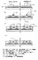
以下に本発明を利用した代表的な形態を示す。本明細書で開示する発明では、図1に示すように、基本的に1つの画素内に1つの表示用半導体装置(TFT)と少なくとも1つの受光用半導体装置(TFT)を有する新規な素子構成とする。そして、この素子の反射電極上に形成された配向膜によって配向された液晶に電加を印加して、液晶表示面で表示を行い、液晶表示面の裏面に入射する光信号をセンサ部で読み取り、映像を取り込む装置とする。本発明のパネル構成図を図4(A)及び図4(B)に示す。また、本発明のパネルおける回路図を簡略に示した図が図3である。
【0024】
図4(A)に示すように、液晶パネルには、表示部およびセンサ部402の周辺に、センサ部を駆動するセンサ駆動回路403と表示部を駆動する表示駆動回路404が設けられているパネル配置となっている。
【0025】
本発明は、センサ部が液晶表示面の裏面に入射する光信号データを読み取り、センサ端子部406に接続される外部記憶装置等にデータを記憶させ、そのデータを画像表示用に加工処理した後、表示引出端子部405から表示部へ入力させることによって、表示部402に映像を映し出すシステムとしている。また、メモリー回路等を同一基板上に形成して、これらのシステムを同一基板で行なう構成としてもよい。そして、センサ部で取り込んだ動画像または静止画像を液晶パネルにおいて、ほぼリアルタイムで表示する。また、表示部においては、装置外部からのデータを表示することが可能な構成としてもよい。
【0026】
図4(B)には、図4(A)中のA−B断面構造の簡略図を示した。素子基板400は、シール材407で対向基板401と貼り合わされており、その間に液晶材料410を挟持している。液晶表示面に入射する光を利用して映像を使用者に提供する。
【0027】
本発明は、裏面に取りつけられた光学系409と、カラーフィルター411を通り、さらに基板400を通り抜けた光信号をセンサ部で感知する。そのため、本発明で使用する基板400は、可視光に対して極めて優れた透明性を有するものを用いることが好ましい。
【0028】
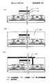
そして、図4中の表示部およびセンサ部402を構成する1画素の断面図を図1に示し、このような素子を用いた配置の一例を図2に示した。
【0029】
図2(A)は、表面上図を示しており、A−Bの断面図が図1に相当する。図2(A)では、センサ部が反射電極121に覆われている。また、図2(A)では、配線106、107、115、116上に反射電極121を形成しない構成とした。この反射電極121を用いて、液晶の表示を行う。ここで、液晶表示に関与する配線は、画素部TFT信号線115と、画素部TFTゲイト線106である。
【0030】
一方、図2(B)は、図2(A)の裏面を示している。また、実際は、TFTの保護遮光膜104、105が形成されているため、TFT部は観察できないが、便宜上、遮光膜104、105の形成箇所のみを示した図面としている。加えて、配線106、107、115、116上及び画素TFT上に光電変換層118を形成してもよいが、図2(B)では、光電変換層118を形成しない構成とした。この光電変換層に入射される光信号を読み取り、センサ部TFT信号線116にデータを送る。ここで、画像読み取りに関与する配線は、センサ部TFT信号線116と、センサ部TFTゲイト線107である。
【0031】
すなわち、本発明は、図1または図2に示すように、1画素内に2つのTFTを有している構成となっているので受光マトリクスと表示マトリクスの画素ピッチ、ビット数は同じになる。表示素子側の基板100上には、遮光膜104が設けられており、裏面から入射する光からTFTを保護する構造としている。また、センサ素子側のTFTに遮光膜105を設ける構成としてもよい。また、この遮光膜は、基板の裏面に直接設ける構成としてもよい。
【0032】
この遮光膜104、105上に下地膜101を形成した後、表示または画像の読み取りを行うためのTFTを複数形成する。ここでいう基板の裏面とは、TFTが形成されていない基板面のことを指している。また、このTFTの構成は、トップゲート型TFTであってもボトムゲート型TFTであっても構わない。
【0033】
そして、センサ素子側のTFTのドレイン電極112と接続する透明導電性膜117を設ける。この導電性膜は、光電変換素子の下部電極をなす膜であり、表示素子のTFTの上部以外の画素領域に形成する。この導電性膜上に光電変換層を設け、さらにその上に上部電極119を設けることで、光電変換素子を完成させる。
【0034】
一方、表示素子側のTFTは、ドレイン配線114と接続する画素反射電極121を設ける。この画素反射電極はセンサ部および配線を覆う構成としてもよい。また、配線を覆う構成とした場合には、配線と画素反射電極との間に存在する絶縁膜を誘電体として、容量が形成される。本発明は、反射型表示であるので画素電極には反射性を有する金属材料を用いる。
【0035】
本発明の製造プロセスは、光電変換素子の作製工程以外、従来の表示装置の作製工程と概略同じである。よって、従来の製造プロセスを用いることができるので、容易に、且つ、安価に作製することができる。また、本発明により作製した装置は、センサ機能を搭載しても、従来のパネルと形状及び大きさは変化しない。そのため、小型化、軽量化することができる。
【0036】
【実施例】
以下、本発明の実施例を説明するが、本発明がこの実施例に限定されないことは勿論である。
〔実施例1〕
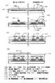
本実施例においては、液晶表示面の裏面から受光するセンサ部を有する液晶パネルの作製工程例を図5、6を用いて詳述する。
【0037】
まず、透明基板100全面に下地膜101を形成する。透明基板100としては、透明性を有するガラス基板や石英基板を用いることができる。下地膜として、プラズマCVD法によって、酸化珪素膜を150nmの厚さに形成した。本実施例では、この下地膜形成工程前に、表示画素部TFTを裏面からの光から保護するための遮光膜104、受光センサ部TFTを裏面からの光から保護するための遮光膜105を設けた。本実施例では、ノイズおよび劣化を防止するために遮光膜を設けたが、開口率を優先するのであれば特に設ける必要はない。
【0038】
次に、プラズマCVD法によって非晶質珪素膜を30〜100nm好ましくは30nmの厚さに成膜し、エキシマレーザ光を照射して、多結晶珪素膜を形成した。なお、非晶質珪素膜の結晶化方法として、SPCと呼ばれる熱結晶化法、赤外線を照射するRTA法、熱結晶化とレーザアニールとの用いる方法等を用いてもよい。
【0039】
次に、多結晶珪素膜をパターニングして、TFT200、300のソース領域、ドレイン領域、チャネル形成領域を構成する島状の半導体層102を形成する。そして、これら半導体層を覆うゲイト絶縁膜103を形成する。ゲイト絶縁膜はシラン(SiH4 )とN2 Oを原料ガスに用いて、プラズマCVD法で100nmの厚さに形成する。〔図5(A)〕
【0040】
次に、導電膜を形成する。ここでは、導電膜材料として、アルミニウムを用いたが、チタン、または、シリコンを主成分とする膜、もしくは、それらの積層膜であってもよい。本実施例では、スパッタ法でアルミニウム膜を200〜500nmの厚さ、代表的には300nmに形成する。ヒロックやウィスカーの発生を抑制するために、アルミニウム膜にはスカンジウム(Sc)やチタン(Ti)やイットリウム(Y)を0.04〜1.0重量%含有させる。
【0041】
次に、レジストマスクを形成し、アルミニウム膜をパターニングして、電極パターンを形成し、画素ゲイト電極106、センサ部ゲイト電極107を形成する。
【0042】
次に、公知の方法によりオフセット構造を形成する。更に、公知の方法により、LDD構造を形成してもよい。〔図5(B)〕
【0043】
そして、第1の層間絶縁膜113を形成し、N型高濃度不純物領域(ソース領域、ドレイン領域)に達するコンタクトホールを形成する。しかる後、金属膜を形成し、パターニングして、配線112、114、115、116を形成する。
【0044】
本実施例では、第1の層間絶縁膜113を厚さ500nmの窒化珪素膜で形成する。第1の層間絶縁膜として、窒化珪素膜の他に、酸化珪素膜、窒化珪素膜を用いることができる。また、これらの絶縁膜の多層膜としても良い。
【0045】
また、配線の出発膜となる金属膜として、本実施例では、スパッタ法で、チタン膜、アルミニウム膜、チタン膜でなる積層膜を形成する。これらの膜厚はそれぞれ100nm、300nm、100nmとする。
【0046】
以上のプロセスを経て、画素TFT200、受光部TFT300が同時に完成する。〔図5(C)〕
【0047】
次に、第1の層間絶縁膜113に受光部TFTのドレイン配線112に接して透明導電膜を形成する。透明導電膜を成膜し、パターニングして、光電変換素子の透明電極117を形成する。透明導電膜117にはITOやSnO2 を用いることができる。本実施例では、透明導電膜として厚さ100nmのITO膜を形成する。
【0048】
一般的なアクティブ型のイメージセンサが上部電極を透明導電膜で形成しているのに対し、本実施例のイメージセンサは下部電極を透明導電膜で形成している点で異なっている。本発明においては、裏面から受光するため、下部電極を透明導電膜で形成する。〔図5(D)〕
【0049】
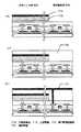
次に、光電変換層として機能する、水素を含有する非晶質珪素膜118(以下、a−Si:H膜と表記する)を基板全面に成膜する。そして、受光部だけにa−Si:H膜が残存するようにパターニングをし、光電変換層とする。
【0050】
次に、基板全面に導電膜を形成する。本実施例では導電膜として厚さ200nmのチタン膜をスパッタ法で成膜する。この導電膜をパターニングし、受光部TFTに接続された上部電極119を形成する。この導電膜としてチタン、クロムを用いることができる。〔図6(A)〕
【0051】
このセンサ部の受光有効箇所は、ゲイト配線106、107と信号配線115、116で囲まれた1つの画素内の遮光膜104、105が形成されていない箇所となる。本実施例での画素サイズは、表示部とセンサ部で同じであり、60×60μmとしたが、16×16μm〜70×70μmの範囲であれば、特に限定されない。
【0052】
そして、第2の層間絶縁膜120を形成する。第3の層間絶縁膜を構成する絶縁被膜として、ポリイミド、ポリアミド、ポリイミドアミド、アクリル等の樹脂膜を形成すると平坦な表面を得ることができるため、好ましい。あるいは積層構造とし、第3の層間絶縁膜の上層は上記の樹脂膜、下層は酸化珪素、窒化珪素、酸化窒化珪素等の無機絶縁材料の単層、多層膜を成膜してもよい。本実施例では、絶縁被膜として厚さ0.7μmのポリイミド膜を基板全面に形成した。〔図6(B)〕
【0053】
更に、第2の層間絶縁膜にドレイン配線114に達するコンタクトホールを形成する。再度、基板全面に導電膜を成膜し、パターニングして、画素TFTに接続された画素電極121を形成する。本実施例では導電膜として厚さ200nmのチタン膜をスパッタ法で成膜する。この導電膜としてチタン、クロム、アルミニウムを用いることができる。
【0054】
以上の工程を経て、図6(C)、または、図1に示すような素子基板が完成する。
【0055】
そして、この素子基板と、対向基板とをシール材とで貼り合わせ、液晶を封入して反射型液晶パネルが完成する。液晶は液晶の動作モ─ド(ECBモード、ゲストホストモ─ド)によって自由に選定することができる。また、この対向基板は、透過性基板上に透明導電膜、配向膜を形成して構成される。これ以外にも必要に応じてブラックマスクやカラーフィルターを設けることができる。
【0056】
続いて、図4(B)に示すように、この液晶パネルの裏面に、カラーフィルター411と、光学系409と、光学系409を取りつけるための支持台408を設け、装置を作製する。
【0057】
こうして、液晶表示面の裏面から受光するセンサ部を有する液晶パネルが完成する。また、便宜上、2×2画素に簡略化した本実施例の回路図を図3に示す。この回路図で最も特徴のある点は、液晶表示素子とセンサ素子が、お互いに独立している点である。
【0058】
液晶表示素子は、主に、液晶材料302と、容量314と、画素TFT303と、表示ゲイトドライバ311に接続されたゲイト線と、表示信号ドライバ310と表示入力信号線306、と固定電位線304で構成されている。
【0059】
センサ素子は、主に、フォトダイオードPD301と、センサTFT312と、センサの出力信号線と、センサ水平シフトレジスタ308と、センサ垂直シフトレジスタ309、と固定電位線305で構成されている。
【0060】
〔実施例2〕
本実施例においては、液晶表示面の裏面から受光するセンサ部を有する液晶パネルの作製工程例を図8、9を用いて詳述する。
1つの画素に、表示画素部TFTと、受光センサ部TFTとを有し、これらのTFTを覆って層間膜を形成し、その上に光電変換層を設け、受光センサ部TFTと接続していることが本実施例の特徴である。そのため、実施例1と比較して、開口率が大きい。
【0061】
まず、透明基板全面に下地膜701を形成する。透明基板700としてガラス基板や石英基板を用いることができる。下地膜として、プラズマCVD法によって、酸化珪素膜を200nmの厚さに形成した。本実施例では、この下地膜形成工程前に、表示画素TFT部を裏面からの光から守るための遮光膜703、受光センサTFT部を裏面からの光から守るための遮光膜706を設けた。
【0062】
次に、プラズマCVD法によって非晶質珪素膜を30〜100nm好ましくは30nmの厚さに成膜し、エキシマレーザ光を照射して、多結晶珪素膜を形成した。なお、非晶質珪素膜の結晶化方法として、SPCと呼ばれる熱結晶化法、赤外線を照射するRTA法、熱結晶化とレーザアニールとの用いる方法等を用いることができる。
【0063】
次に、多結晶珪素膜をパターニングして、TFT800、900のソース領域、ドレイン領域、チャネル形成領域を構成する島状の半導体層702を形成する。次に、これら半導体層を覆うゲイト絶縁膜704を形成する。ゲイト絶縁膜はシラン(SiH4 )とN2 Oを原料ガスに用いて、プラズマCVD法で120nmの厚さに形成する。〔図8(A)〕
【0064】
次に、導電膜を形成する。ここでは、導電膜材料として、アルミニウムを用いたが、チタン、または、シリコンを主成分とする膜、もしくは、それらの積層膜であってもよい。本実施例では、スパッタ法でアルミニウム膜を300〜500nmの厚さ、代表的には300nmに形成する。ヒロックやウィスカーの発生を抑制するために、アルミニウム膜にはスカンジウム(Sc)やチタン(Ti)やイットリウム(Y)を0.04〜1.0重量%含有させる。
【0065】
次に、レジストマスクを形成し、アルミニウム膜をパターニングして、電極パターンを形成し、ゲイト電極705、707を形成する。
【0066】
次に、公知の方法によりLDD構造709、710を形成する。更に、公知の方法により、オフセット構造を形成してもよい。708、711は、高濃度不純物領域、712はチャネル領域を示している。〔図8(B)〕
【0067】
そして、第1の層間絶縁膜713を形成し、N型高濃度不純物領域(ソース領域、ドレイン領域)に達するコンタクトホールを形成する。しかる後、金属膜を形成し、パターニングして、配線714、715、722、723を形成する。
【0068】
本実施例では、第1の層間絶縁膜を厚さ500nmの窒化珪素膜で形成する。
第1の層間絶縁膜として、窒化珪素膜の他に、酸化珪素膜、窒化珪素膜を用いることができる。また、これらの絶縁膜の多層膜としても良い。
【0069】
また、配線電極714、715、722、723の出発膜となる金属膜として、本実施例では、スパッタ法で、チタン膜、アルミニウム膜、チタン膜でなる積層膜を形成する。これらの膜厚はそれぞれ100nm、300nm、100nmとする。
【0070】
以上のプロセスを経て、画素TFT800、受光部TFT900が同時に完成する。〔図8(C)〕
【0071】
次に、TFTを覆う、第2の層間絶縁膜716を形成する。実施例1と異なる主な点は、この第2の層間絶縁膜を設けることにより、後の工程で形成される光電変換層を広く形成することができる点である。こうすることによって、実施例1よりセンサの受光面積(開口率)を上げることができる。第2の層間絶縁膜としては、下層の凹凸を相殺して、平坦な表面が得られる樹脂膜が好ましい。このような樹脂膜として、ポリイミド、ポリアミド、ポリイミドアミド、アクリルを用いることができる。また、第2の層間絶縁膜の表面層は平坦な表面を得るため樹脂膜とし、下層は酸化珪素、窒化珪素、酸化窒化珪素等の無機絶縁材料の単層、多層としても良い。本実施例では、第2の層間絶縁膜としてポリイミド膜を1.5μmの厚さに形成する。
【0072】
次に、第2の層間絶縁膜716に受光部TFT900の配線723に達するコンタクトホールを形成した後、透明導電膜を形成する。透明導電膜にはITOやSnO2 を用いることができる。本実施例では、透明導電膜として厚さ120nmのITO膜を形成する。
【0073】
次に、透明導電膜をパターニングし、受光部TFT900に接続された下側電極717を形成する。〔図8(D)〕
【0074】
次に、光電変換層として機能する、水素を含有する非晶質珪素膜718(以下、a−Si:H膜と表記する)を基板全面に成膜する。そして、受光部だけにa−Si:H膜が残存するようにパターニングをし、光電変換層とする。
【0075】
次に、基板全面に導電膜を形成する。本実施例では導電膜として厚さ200nmのチタン膜をスパッタ法で成膜する。この導電膜をパターニングし、受光部TFTに接続された上部電極719を形成する。この導電膜としてチタン、クロムを用いることができる。
【0076】
一般的なアクティブ型のイメージセンサが上部電極を透明電極で形成しているのに対し、本実施例のイメージセンサは下部電極を透明電極で形成している点で異なっている。本発明においては、裏面から受光するため、下部電極を透明導電膜で形成する。〔図9(A)〕
【0077】
そして、第3の層間絶縁膜720を形成する。第3の層間絶縁膜を構成する絶縁被膜として、ポリイミド、ポリアミド、ポリイミドアミド、アクリル等の樹脂膜を形成すると平坦な表面を得ることができるため好ましい。あるいは第3の層間絶縁膜の表面層は上記の樹脂膜とし、下層は酸化珪素、窒化珪素、酸化窒化珪素等の無機絶縁材料の単層、多層膜を成膜してもよい。本実施例では、絶縁被膜として厚さ0.5μmのポリイミド膜を基板全面に形成した。〔図9(B)〕
【0078】
また、ポリイミド成膜後の本発明の最高プロセス温度は、このポリイミドの耐熱温度320℃より低い温度になるようにする。
【0079】
更に、第3、第2の層間絶縁膜に配線に達するコンタクトホールを形成する。
再度、基板全面に導電膜を成膜し、パターニングして、画素TFTに接続された画素電極721を形成する。本実施例では導電膜として厚さ200nmのチタン膜をスパッタ法で成膜する。この導電膜としてチタン、クロムを用いることができる。
【0080】
以上の工程を経て、図9(C)、または、図7に示すような素子基板が完成する。
【0081】
この後は、実施例1と同様に、素子基板と、対向基板とをシール材とで貼り合わせ、液晶を封入して反射型液晶パネルを完成させ、この液晶パネルの裏面に、カラーフィルター411と、光学系409と、光学系409を取りつけるための支持台408を設け、装置を作製する。
【0082】
こうして、液晶表示面の裏面から受光するセンサ部を有する液晶パネルが完成する。
【0083】
〔実施例3〕
実施例1、2では、非増幅型のイメージセンサを用いた例を示したが、本実施例では、増幅型のイメージセンサに関し、より具体的には半導体装置をマトリクス状に配置したイメージセンサを用いた例を示す。
【0084】
この増幅型のイメージセンサを用いた液晶パネルの回路図を簡略化した図を図10に示す。増幅型のイメージセンサは、リセットトランジスタT1 と増幅トランジスタT2 と選択トランジスタT3 の3つのTFTを用いるものである。この回路図で最も特徴のある点は、リセット線1012、電源線1113、センサ垂直周辺駆動回路1009、センサ水平周辺駆動回路1008、固定電位線1115を有している点である。
【0085】
また、本実施例は、実施例1または2と同様に液晶表示素子の配線とセンサ素子の配線が、お互いに独立している点が特徴である。液晶表示素子は、液晶1002と、画素TFT1003と、容量1114と、固定電位線1004と、表示ゲイトドライバ1011に接続されたゲイト線と、表示信号ドライバ1010と表示入力信号線1006で構成されている。
【0086】
一般的なアクティブ型のイメージセンサが上部電極を透明電極で形成しているのに対し、本実施例のイメージセンサは下部電極を透明電極で形成している点で異なっている。
【0087】
本実施例のイメージセンサの動作方法は、1フレーム分の画像が検出されると、リセット線1012からリセットパルス信号が入力され、リセット線をゲイトに有するリセットトランジスタT1 がオン状態になる。するとフォトダイオ─ドの上部電極および増幅トランジスタの電位が電源電位にリセットされる。リセットトランジスタT1 がオフ状態では、増幅トランジスタT2 のゲイト電極は浮遊状態となる。この状態でフォトダイオードPD1001において入射した光が電荷に変換され蓄積される。この電荷によりフォトダイオードの上部電極の電位が電源電位から微少に変化する。この電位の変動は増幅トランジスタT2 のゲイト電極の電位変動として検出され、増幅トランジスタT2 のドレイン電流が増幅される。選択線1116から選択パルス信号が入力されると、選択トランジスタT3 はオン状態とされ、増幅トランジスタT2 において増幅された電流を映像信号として信号線1007に出力するしくみとなっている。
【0088】
〔実施例4〕
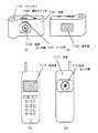
本実施例では、実施例1〜3に示すようなイメージセンサ機能を有する一体型液晶表示パネルを備えた装置の例を示す。
【0089】
ここでは、図11(A)、(B)で示すようなデジタルスチールカメラの例を示す。図11(A)、(B)は、見る角度を180度異ならせた場合のものである。
【0090】
図11(A)、(B)に示す構成は、本体1101に表示部1106とその裏面に配置されたイメージセンサが配置された受光部1102、さらに操作スイッチ1105、シャッター1104、ストロボ1103を備えている。
【0091】
受光部1102のイメージセンサで捉えた像は、信号処理されて、静止画または動画をリアルタイムに表示またはメモリに取り込む。
【0092】
また、ここでは、図11(C)、(D)で示すようなセンサ機能を有する携帯電話の例を示す。図11(C)、(D)は、見る角度を180度異ならせた場合のものである。
【0093】
図11(C)、(D)に示す構成は、本体1111に表示部1117とその裏面に配置されたイメージセンサが配置された受光部1112、さらに操作スイッチを備えている。
【0094】
受光部1112のイメージセンサで捉えた像は、信号処理されて、静止画または動画をリアルタイムに表示部1117で表示する。また、通信相手から画像データを受け取り表示させる。さらに、受光部1112のイメージセンサで捉えた画像データをメモリに取り込み、通信相手に画像データを送信する構成としてもよい。
【0095】
【発明の効果】
本発明の製造プロセスは、光電変換素子の作製工程以外、従来の表示装置と同じである。よって、従来の製造プロセスを用いることができるので、容易に、且つ、安価に作製することができる。また、本発明により作製した装置は、センサ機能を搭載しても、従来のパネルと基板形状及び大きさは変化しない。そのため、小型化、軽量化することができる。
【0096】
また、センサセルの受光面積は、表示セルの画素面積の概略同程度であり、単結晶CCDと比較して大きいため、本発明のセンサは高感度とすることができる。さらに、本構成で消費される電力は僅かであり、またイメージセンサで消費される電力もCCD構造に比較すれば小さいものとすることができる。
【図面の簡単な説明】
【図1】 本発明の画素断面図
【図2】 1つの画素の表面配置図及び裏面配置図の一例。
【図3】 本発明の回路図
【図4】 液晶パネル全体図
【図5】 1つの画素にセンサ部と表示素子を形成する工程を示す図。
【図6】 1つの画素にセンサ部と表示素子を形成する工程を示す図。
【図7】 実施例2の画素断面図
【図8】 実施例2における作製工程図
【図9】 実施例2における作製工程図
【図10】 実施例3の回路図
【図11】 本発明の応用例
【符号の説明】
100 基板
101 下地膜
102 島状の半導体層
103 ゲイト絶縁膜
104 遮光膜(画素部TFT)
105 遮光膜(センサ部TFT)
106 ゲイト電極(画素部TFT)
107 ゲイト電極(センサ部TFT)
108 ソース領域(高濃度不純物領域)
109 ドレイン領域
110 チャネル領域
112 ドレイン電極(センサ部)
113 第1層間絶縁膜
114 ソ─ス線(電極)
115 信号線(画素部)
116 信号線(センサ部)
117 透明導電性膜(下部電極)
118 光電変換層
119 上部電極
120 第2層間絶縁膜
121 画素電極
200 表示画素部
300 受光センサ部
700 基板
701 下地膜
702 島状の半導体層
703 ゲイト絶縁膜
704 遮光膜(画素部TFT)
705 ゲイト電極(画素部TFT)
706 遮光膜(センサ部TFT)
707 ゲイト電極(センサ部TFT)
708 ソース領域(高濃度不純物領域)
709 低濃度不純物領域
710 LDD領域(低濃度不純物領域)
711 ドレイン領域
712 チャネル領域
713 第1層間絶縁膜
716 第2層間絶縁膜
717 透明導電性膜(下部電極)
718 光電変換層
719 上部電極
720 第3層間絶縁膜
721 画素電極
800 表示画素部
900 受光センサ部[0001]
[Technical field to which the invention belongs]
The present invention relates to an image sensor function and a device having a display function. In particular, the present invention relates to an active matrix panel having a display unit composed of a pixel unit composed of a plurality of pixel electrodes arranged in a matrix, and a portable unit having a display unit. The present invention relates to a terminal device, an electronic device such as a personal computer having a display portion, and a manufacturing method thereof.
[0002]
[Prior art]
In recent years, TFT technology using polycrystalline silicon called polysilicon TFT has been intensively studied. As a result, it is possible to fabricate a drive circuit such as a shift register circuit by using a polysilicon TFT, and an active matrix type liquid crystal in which a pixel portion and a peripheral drive circuit for driving the pixel portion are integrated on the same substrate. Panels have come into practical use. Therefore, liquid crystal panels are reduced in cost, size, and weight, and are used in various information devices such as personal computers, mobile phones, video cameras and digital cameras, and display portions of mobile devices.
[0003]
Recently, a pocket-sized small portable information processing terminal device that is more portable than a notebook personal computer and is inexpensive has been put into practical use, and an active matrix liquid crystal panel is used for its display unit. Such an information processing terminal device can input data from a display unit by a touch pen method, but in order to input text / graphics information and video information on a paper surface, an image of a scanner or a digital camera is read. It is necessary to connect with peripheral equipment for Therefore, the portability of the information processing terminal device is impaired. It also puts an economic burden on the user to purchase peripheral equipment.
[0004]
Active matrix display devices are also used in display units of TV conference systems, TV phones, Internet terminals, and the like. These systems and terminals include a camera (CCD camera) that captures images of a conversation person or user, but the display unit and the reading unit (sensor unit) are individually manufactured and modularized. Therefore, the manufacturing cost is high.
[0005]
[Problems to be solved by the invention]
An object of the present invention is to solve the above-described problems and to have a pixel matrix, an image sensor, and a peripheral circuit for driving them, that is, a novel semiconductor that has both an imaging function and a display function and is intelligent It is to provide a display device using the device.
[0006]
A further object of the present invention is to manufacture a display device using a new intelligent semiconductor device at low cost by making the image sensor consistent with the pixel matrix, peripheral drive circuit and structure / manufacturing process. There is.
[0007]
[Means for Solving the Problems]
In order to solve the above problems, the present invention has a configuration in which a display semiconductor device and a light receiving semiconductor device are provided over the same substrate. In addition, the liquid crystal display unit including the pixel electrode and the display semiconductor device and the sensor unit including the light receiving semiconductor device are not separately disposed, but the display semiconductor device and the light receiving semiconductor device are provided in one pixel. By adopting a novel element configuration, that is, a configuration having a semiconductor device (insulated gate field effect semiconductor device) that controls both display and light reception in one pixel, as shown in FIG. 1 or FIG. A display device having an image reading function is reduced in size and size.
[0008]
The first configuration of the invention disclosed in this specification is:
A display unit comprising a pixel matrix having at least a pixel electrode in a matrix and a first semiconductor device connected to the pixel electrode;
At least a photoelectric conversion element and a sensor unit made of a second semiconductor device connected to the photoelectric conversion element are provided on the same substrate surface,
An integrated liquid crystal display panel having an image sensor function, wherein light from the back surface of the substrate is received by the sensor unit.
[0009]
The second configuration of the present invention is as follows.
A display unit comprising a pixel matrix having at least a pixel electrode in a matrix and a first semiconductor device connected to the pixel electrode;
At least a photoelectric conversion element and a sensor unit made of a second semiconductor device connected to the photoelectric conversion element are provided on the same substrate surface,
The display unit and the sensor unit have the same pixel size,
An integrated liquid crystal display panel having an image sensor function, wherein light from the back surface of the substrate is received by the sensor unit.
[0010]
The third configuration of the present invention is as follows.
A display unit comprising a pixel matrix having at least a pixel electrode in a matrix and a first semiconductor device connected to the pixel electrode;
At least a photoelectric conversion element and a sensor unit made of a second semiconductor device connected to the photoelectric conversion element are provided on the same substrate,
The first semiconductor device and the second semiconductor device are provided in the same matrix,
The pixel electrode connected to the first semiconductor device is an integrated liquid crystal display panel having an image sensor function, wherein the pixel electrode exists above the second semiconductor device.
[0011]
The fourth configuration of the present invention is as follows.
A display unit comprising a pixel matrix having at least a pixel electrode in a matrix and a first semiconductor device connected to the pixel electrode;
At least a photoelectric conversion element and a sensor unit made of a second semiconductor device connected to the photoelectric conversion element are provided on the same substrate,
The photoelectric conversion element is composed of at least an upper electrode, a photoelectric conversion layer, and a lower electrode,
The upper electrode is made of a metal having reflectivity for at least visible light,
An integrated liquid crystal display panel having an image sensor function, wherein the lower electrode is made of a transparent conductive film.
[0012]
The fifth configuration of the present invention is as follows.
A pixel electrode having a pixel electrode arranged in a matrix and a first semiconductor device connected to the pixel electrode;
A method for manufacturing an integrated liquid crystal display panel having an image sensor function, in which an image sensor having a light receiving portion having a photoelectric conversion element and a second semiconductor device connected to the photoelectric conversion element is provided on the same substrate Because
A first step of manufacturing the first semiconductor device and the second semiconductor device on the substrate;
A second step of forming a lower electrode made of a translucent conductive film connected to the second semiconductor device;
A third step of forming a photoelectric conversion layer on the lower electrode;
A fourth step of forming an upper electrode in contact with the photoelectric conversion layer; and a method for manufacturing an integrated liquid crystal display panel having an image sensor function.
[0013]
The sixth configuration of the present invention is as follows.
A pixel electrode having a pixel electrode arranged in a matrix and a first semiconductor device connected to the pixel electrode;
A method for manufacturing an integrated liquid crystal display panel having an image sensor function, in which an image sensor having a light receiving portion having a photoelectric conversion element and a second semiconductor device connected to the photoelectric conversion element is provided on the same substrate Because
A first step of manufacturing the first semiconductor device and the second semiconductor device on the substrate;
A second step of forming a first insulating film covering at least the first semiconductor device and the second semiconductor device;
A third step of forming a translucent conductive film on the first insulating film;
A fourth step of patterning the translucent conductive film to form a lower electrode connected to the second semiconductor device;
A fifth step of forming a photoelectric conversion layer on the lower electrode;
A sixth step of forming an upper electrode in contact with the photoelectric conversion layer; and a method for manufacturing an integrated liquid crystal display panel having an image sensor function.
[0014]
The seventh configuration of the present invention is as follows.
The photoelectric conversion element is composed of a lower electrode, a photoelectric conversion layer formed on the lower electrode, and an upper electrode formed on the photoelectric conversion layer,
A sensor unit comprising at least one active element connected to the photoelectric conversion element is provided on an insulating substrate;
The upper electrode is made of a metal having reflectivity for at least visible light,
An integrated liquid crystal display panel having an image sensor function, wherein the lower electrode is made of a conductive film having transparency to at least visible light.
[0015]
The eighth configuration of the present invention is as follows.
A display unit comprising a pixel matrix having at least a pixel electrode in a matrix and an active element connected to the pixel electrode;
At least a photoelectric conversion element and a sensor unit composed of an active element group connected to the photoelectric conversion element are provided on the same substrate surface,
An integrated liquid crystal display panel having an image sensor function, wherein light from the back surface of the substrate is received by the sensor unit.
[0016]
The ninth configuration of the present invention is as follows.
A display unit comprising a pixel matrix having at least a pixel electrode in a matrix and an active element connected to the pixel electrode;
At least a photoelectric conversion element and a sensor unit composed of an active element group connected to the photoelectric conversion element are provided on the same substrate surface,
The display unit and the sensor unit have the same pixel size,
An integrated liquid crystal display panel having an image sensor function, wherein light from the back surface of the substrate is received by the sensor unit.
[0017]
The tenth configuration of the present invention is
A display unit comprising a pixel matrix having at least a pixel electrode in a matrix and an active element connected to the pixel electrode;
At least a photoelectric conversion element and a sensor unit composed of an active element group connected to the photoelectric conversion element are provided on the same substrate,
The active element and the active element group are provided in the same matrix,
The pixel electrode connected to the active element exists above the active element group, and is an integrated liquid crystal display panel having an image sensor function.
[0018]
The eleventh configuration of the present invention is
A display unit comprising a pixel matrix having at least a pixel electrode in a matrix and an active element connected to the pixel electrode;
At least a photoelectric conversion element and a sensor unit composed of an active element group connected to the photoelectric conversion element are provided on the same substrate,
The photoelectric conversion element is composed of at least an upper electrode, a photoelectric conversion layer, and a lower electrode,
The upper electrode is made of a metal having reflectivity for at least visible light,
An integrated liquid crystal display panel having an image sensor function, wherein the lower electrode is made of a transparent conductive film.
[0019]
In the eighth to eleventh configurations, the active element group includes at least an amplification transistor, a reset transistor, and a selection transistor.
[0020]
The twelfth configuration of the present invention is
Pixel electrodes arranged in a matrix, and a pixel matrix having active elements connected to the pixel electrodes;
An image sensor having a light receiving portion having a photoelectric conversion element and an active element group connected to the photoelectric conversion element is a method for manufacturing an integrated liquid crystal display panel having an image sensor function provided on the same substrate. And
A first step of producing the active element and the active element group on the substrate;
A second step of forming a lower electrode made of a translucent conductive film connected to the active element group;
A third step of forming a photoelectric conversion layer on the lower electrode;
A fourth step of forming an upper electrode in contact with the photoelectric conversion layer; and a method for manufacturing an integrated liquid crystal display panel having an image sensor function.
[0021]
The thirteenth configuration of the present invention is
Pixel electrodes arranged in a matrix, and a pixel matrix having active elements connected to the pixel electrodes;
An image sensor having a light receiving portion having a photoelectric conversion element and an active element group connected to the photoelectric conversion element is a method for manufacturing an integrated liquid crystal display panel having an image sensor function provided on the same substrate. And
A first step of producing the active element and the active element group on the substrate;
A second step of forming a first insulating film covering at least the active element and the active element group;
A third step of forming a translucent conductive film on the first insulating film;
Patterning the translucent conductive film to form a lower electrode connected to the active element group;
A fifth step of forming a photoelectric conversion layer on the lower electrode;
And a sixth step of forming an upper electrode in contact with the photoelectric conversion layer. A method for manufacturing an integrated liquid crystal display panel having an image sensor function.
[0022]
In the twelfth or thirteenth configuration of the present invention, the active element group includes at least an amplification transistor, a reset transistor, and a selection transistor.
[0023]
DETAILED DESCRIPTION OF THE INVENTION
The following are typical forms using the present invention. In the invention disclosed in this specification, as shown in FIG. 1, a novel element configuration basically having one display semiconductor device (TFT) and at least one light receiving semiconductor device (TFT) in one pixel. And Then, an electric voltage is applied to the liquid crystal aligned by the alignment film formed on the reflective electrode of this element, display is performed on the liquid crystal display surface, and an optical signal incident on the back surface of the liquid crystal display surface is read by the sensor unit. Suppose that the device captures video. 4A and 4B show a panel configuration diagram of the present invention. FIG. 3 is a simplified circuit diagram of the panel of the present invention.
[0024]
As shown in FIG. 4A, the liquid crystal panel is provided with a
[0025]
In the present invention, after the sensor unit reads optical signal data incident on the back surface of the liquid crystal display surface, the data is stored in an external storage device connected to the sensor terminal unit 406, and the data is processed for image display. In this system, an image is displayed on the
[0026]
FIG. 4B is a simplified diagram of a cross-sectional structure taken along the line AB in FIG. The
[0027]
In the present invention, an optical signal passing through the optical system 409 and the
[0028]
A cross-sectional view of one pixel constituting the display unit and
[0029]
FIG. 2A shows a top view, and a cross-sectional view taken along line AB corresponds to FIG. In FIG. 2A, the sensor portion is covered with the
[0030]
On the other hand, FIG. 2B shows the back surface of FIG. Actually, since the TFT protective light-shielding
[0031]
That is, according to the present invention, as shown in FIG. 1 or FIG. 2, since two TFTs are provided in one pixel, the pixel pitch and the number of bits of the light receiving matrix and the display matrix are the same. A
[0032]
After the
[0033]
Then, a transparent
[0034]
On the other hand, the TFT on the display element side is provided with a
[0035]
The manufacturing process of the present invention is substantially the same as the manufacturing process of the conventional display device except for the manufacturing process of the photoelectric conversion element. Therefore, since the conventional manufacturing process can be used, it can be manufactured easily and inexpensively. In addition, the device manufactured according to the present invention is not changed in shape and size from the conventional panel even if the sensor function is mounted. Therefore, it can be reduced in size and weight.
[0036]
【Example】
Examples of the present invention will be described below, but the present invention is of course not limited to these examples.
[Example 1]
In this embodiment, a manufacturing process example of a liquid crystal panel having a sensor portion that receives light from the back surface of the liquid crystal display surface will be described in detail with reference to FIGS.
[0037]
First, the
[0038]
Next, an amorphous silicon film was formed to a thickness of 30 to 100 nm, preferably 30 nm, by plasma CVD, and irradiated with excimer laser light to form a polycrystalline silicon film. Note that as a method for crystallizing the amorphous silicon film, a thermal crystallization method called SPC, an RTA method of irradiating infrared rays, a method using thermal crystallization and laser annealing, or the like may be used.
[0039]
Next, the polycrystalline silicon film is patterned to form an island-shaped
[0040]
Next, a conductive film is formed. Here, aluminum is used as a conductive film material, but a film containing titanium or silicon as a main component or a stacked film thereof may be used. In this embodiment, an aluminum film is formed to a thickness of 200 to 500 nm, typically 300 nm, by sputtering. In order to suppress generation of hillocks and whiskers, the aluminum film contains scandium (Sc), titanium (Ti), and yttrium (Y) in an amount of 0.04 to 1.0% by weight.
[0041]
Next, a resist mask is formed, the aluminum film is patterned to form an electrode pattern, and a
[0042]
Next, an offset structure is formed by a known method. Further, the LDD structure may be formed by a known method. [Fig. 5 (B)]
[0043]
Then, a first
[0044]
In this embodiment, the first
[0045]
In this embodiment, a laminated film made of a titanium film, an aluminum film, and a titanium film is formed as a metal film to be a wiring starting film by sputtering. These film thicknesses are 100 nm, 300 nm, and 100 nm, respectively.
[0046]
Through the above process, the pixel TFT 200 and the light receiving portion TFT 300 are completed simultaneously. [Fig. 5 (C)]
[0047]
Next, a transparent conductive film is formed on the first
[0048]
A general active image sensor is different from the image sensor of this embodiment in that the lower electrode is formed of a transparent conductive film, whereas the upper electrode is formed of a transparent conductive film. In the present invention, in order to receive light from the back surface, the lower electrode is formed of a transparent conductive film. [Fig. 5 (D)]
[0049]
Next, an
[0050]
Next, a conductive film is formed over the entire surface of the substrate. In this embodiment, a titanium film having a thickness of 200 nm is formed as the conductive film by a sputtering method. The conductive film is patterned to form an
[0051]
The light receiving effective part of the sensor unit is a part where the
[0052]
Then, a second
[0053]
Further, a contact hole reaching the
[0054]
Through the above steps, an element substrate as shown in FIG. 6C or FIG. 1 is completed.
[0055]
Then, the element substrate and the counter substrate are bonded together with a sealing material, and liquid crystal is sealed to complete a reflective liquid crystal panel. The liquid crystal can be freely selected according to the operation mode of the liquid crystal (ECB mode, guest host mode). The counter substrate is configured by forming a transparent conductive film and an alignment film on a transparent substrate. In addition to this, a black mask and a color filter can be provided as necessary.
[0056]
Subsequently, as shown in FIG. 4B, a
[0057]
Thus, a liquid crystal panel having a sensor portion that receives light from the back surface of the liquid crystal display surface is completed. For convenience, FIG. 3 shows a circuit diagram of this embodiment simplified to 2 × 2 pixels. The most characteristic point in this circuit diagram is that the liquid crystal display element and the sensor element are independent of each other.
[0058]
The liquid crystal display element mainly includes a
[0059]
The sensor element mainly includes a photodiode PD301, a
[0060]
[Example 2]
In this embodiment, a manufacturing process example of a liquid crystal panel having a sensor portion that receives light from the back surface of the liquid crystal display surface will be described in detail with reference to FIGS.
One pixel has a display pixel portion TFT and a light receiving sensor portion TFT. An interlayer film is formed to cover these TFTs, a photoelectric conversion layer is provided thereon, and is connected to the light receiving sensor portion TFT. This is a feature of this embodiment. Therefore, compared with Example 1, the aperture ratio is large.
[0061]
First, a
[0062]
Next, an amorphous silicon film was formed to a thickness of 30 to 100 nm, preferably 30 nm, by plasma CVD, and irradiated with excimer laser light to form a polycrystalline silicon film. Note that as a method for crystallizing the amorphous silicon film, a thermal crystallization method called SPC, an RTA method of irradiating infrared rays, a method using thermal crystallization and laser annealing, or the like can be used.
[0063]
Next, the polycrystalline silicon film is patterned to form an island-shaped
[0064]
Next, a conductive film is formed. Here, aluminum is used as a conductive film material, but a film containing titanium or silicon as a main component or a stacked film thereof may be used. In this embodiment, an aluminum film is formed to a thickness of 300 to 500 nm, typically 300 nm, by sputtering. In order to suppress generation of hillocks and whiskers, the aluminum film contains scandium (Sc), titanium (Ti), and yttrium (Y) in an amount of 0.04 to 1.0% by weight.
[0065]
Next, a resist mask is formed, the aluminum film is patterned to form an electrode pattern, and
[0066]
Next,
[0067]
Then, a first
[0068]
In this embodiment, the first interlayer insulating film is formed of a silicon nitride film having a thickness of 500 nm.
In addition to the silicon nitride film, a silicon oxide film or a silicon nitride film can be used as the first interlayer insulating film. Further, a multilayer film of these insulating films may be used.
[0069]
In this embodiment, a laminated film made of a titanium film, an aluminum film, and a titanium film is formed by a sputtering method as a metal film that serves as a starting film for the
[0070]
Through the above process, the pixel TFT 800 and the light receiving portion TFT 900 are completed simultaneously. [Fig. 8 (C)]
[0071]
Next, a second
[0072]
Next, after forming a contact hole reaching the
[0073]
Next, the transparent conductive film is patterned to form a
[0074]
Next, an
[0075]
Next, a conductive film is formed over the entire surface of the substrate. In this embodiment, a titanium film having a thickness of 200 nm is formed as the conductive film by a sputtering method. The conductive film is patterned to form an
[0076]
A general active type image sensor differs from the image sensor of this embodiment in that the lower electrode is formed of a transparent electrode, whereas the upper electrode is formed of a transparent electrode. In the present invention, in order to receive light from the back surface, the lower electrode is formed of a transparent conductive film. [FIG. 9 (A)]
[0077]
Then, a third
[0078]
Further, the maximum process temperature of the present invention after polyimide film formation is set to a temperature lower than the heat resistant temperature 320 ° C. of this polyimide.
[0079]
Further, a contact hole reaching the wiring is formed in the third and second interlayer insulating films.
A conductive film is formed again on the entire surface of the substrate and patterned to form a
[0080]
Through the above steps, an element substrate as shown in FIG. 9C or FIG. 7 is completed.
[0081]
Thereafter, as in Example 1, the element substrate and the counter substrate are bonded together with a sealing material, and a liquid crystal is sealed to complete a reflective liquid crystal panel. On the back surface of the liquid crystal panel, a
[0082]
Thus, a liquid crystal panel having a sensor portion that receives light from the back surface of the liquid crystal display surface is completed.
[0083]
Example 3
In the first and second embodiments, an example in which a non-amplification type image sensor is used has been described. In this embodiment, an amplification type image sensor, more specifically, an image sensor in which semiconductor devices are arranged in a matrix is used. An example used is shown.
[0084]
FIG. 10 shows a simplified circuit diagram of a liquid crystal panel using this amplification type image sensor. The amplifying type image sensor includes a reset transistor T1 And amplification transistor T2 And select transistor TThree These three TFTs are used. The most characteristic point in this circuit diagram is that it includes a
[0085]
Further, the present embodiment is characterized in that the wiring of the liquid crystal display element and the wiring of the sensor element are independent from each other as in the first or second embodiment. The liquid crystal display element includes a
[0086]
A general active type image sensor differs from the image sensor of this embodiment in that the lower electrode is formed of a transparent electrode, whereas the upper electrode is formed of a transparent electrode.
[0087]
In the operation method of the image sensor of this embodiment, when an image for one frame is detected, a reset pulse signal is input from the
[0088]
Example 4
In this embodiment, an example of an apparatus including an integrated liquid crystal display panel having an image sensor function as shown in
[0089]
Here, an example of a digital still camera as shown in FIGS. 11A and 11B is shown. FIGS. 11A and 11B show the case where the viewing angle is changed by 180 degrees.
[0090]
11A and 11B includes a main body 1101 including a
[0091]
The image captured by the image sensor of the
[0092]
Here, an example of a mobile phone having a sensor function as shown in FIGS. 11C and 11D is shown. FIGS. 11C and 11D show cases where the viewing angles are varied by 180 degrees.
[0093]
11C and 11D includes a light receiving portion 1112 in which a main body 1111 is provided with a display portion 1117 and an image sensor arranged on the back surface thereof, and an operation switch.
[0094]
The image captured by the image sensor of the light receiving unit 1112 is subjected to signal processing, and a still image or a moving image is displayed on the display unit 1117 in real time. In addition, image data is received from a communication partner and displayed. Further, the image data captured by the image sensor of the light receiving unit 1112 may be captured in a memory and transmitted to the communication partner.
[0095]
【The invention's effect】
The manufacturing process of the present invention is the same as that of a conventional display device except for the manufacturing process of the photoelectric conversion element. Therefore, since the conventional manufacturing process can be used, it can be manufactured easily and inexpensively. Further, even if the device manufactured according to the present invention is equipped with a sensor function, the shape and size of the conventional panel and the substrate do not change. Therefore, it can be reduced in size and weight.
[0096]
Further, since the light receiving area of the sensor cell is approximately the same as the pixel area of the display cell and is larger than that of the single crystal CCD, the sensor of the present invention can be highly sensitive. Furthermore, the power consumed by this configuration is very small, and the power consumed by the image sensor can be reduced compared to the CCD structure.
[Brief description of the drawings]
FIG. 1 is a cross-sectional view of a pixel of the present invention.
FIG. 2 is an example of a front surface layout diagram and a back surface layout diagram of one pixel.
FIG. 3 is a circuit diagram of the present invention.
[Figure 4] Overall view of the LCD panel
FIG. 5 is a diagram showing a process of forming a sensor portion and a display element in one pixel.
FIG. 6 is a diagram showing a process of forming a sensor portion and a display element in one pixel.
7 is a pixel cross-sectional view of Example 2. FIG.
8 is a manufacturing process diagram in Example 2. FIG.
9 is a manufacturing process diagram in Example 2. FIG.
10 is a circuit diagram of Example 3. FIG.
FIG. 11 shows an application example of the present invention.
[Explanation of symbols]
100 substrates
101 Base film
102 Island-like semiconductor layer
103 Gate insulation film
104 Light-shielding film (pixel unit TFT)
105 Light shielding film (Sensor TFT)
106 Gate electrode (pixel TFT)
107 Gate electrode (Sensor TFT)
108 Source region (high concentration impurity region)
109 Drain region
110 channel region
112 Drain electrode (sensor part)
113 First interlayer insulating film
114 Source wire (electrode)
115 Signal line (pixel part)
116 Signal line (sensor part)
117 Transparent conductive film (lower electrode)
118 Photoelectric conversion layer
119 Upper electrode
120 Second interlayer insulating film
121 pixel electrode
200 Display pixel section
300 Light receiving sensor
700 substrates
701 Base film
702 Island-like semiconductor layer
703 Gate insulation film
704 Light-shielding film (pixel unit TFT)
705 Gate electrode (pixel TFT)
706 Light shielding film (Sensor TFT)
707 Gate electrode (Sensor TFT)
708 source region (high concentration impurity region)
709 Low concentration impurity region
710 LDD region (low concentration impurity region)
711 drain region
712 channel region
713 First interlayer insulating film
716 Second interlayer insulating film
717 Transparent conductive film (lower electrode)
718 photoelectric conversion layer
719 Upper electrode
720 Third interlayer insulating film
721 Pixel electrode
800 Display pixel section
900 Light receiving sensor
Claims (16)
Translated fromJapanese前記第1のトランジスタ及び前記第2のトランジスタは、同一基板上に設けられ、
前記第2のトランジスタの半導体層に電気的に接続されたソース電極及びドレイン電極を覆って第1の絶縁膜が設けられ、
前記光電変換素子は、前記第1の絶縁膜上に下部電極と、前記下部電極上に形成された光電変換層と、前記光電変換層上に形成された上部電極とを有し、
前記第1の絶縁膜及び前記光電変換素子上に第2の絶縁膜が形成され、
前記第2の絶縁膜上に前記画素電極が設けられ、
前記光電変換素子は、前記第1の絶縁膜に設けられたコンタクトホールを介して前記ドレイン電極に前記下部電極が電気的に接続され、かつ、前記第2のトランジスタと重なるように前記第1の絶縁膜上に設けられていることを特徴とするアクティブマトリクス型表示装置。One pixel includes a pixel electrode, a firsttransistorelectrically connected to the pixel electrode, a photoelectric conversion element, anda secondtransistorelectrically connected to the photoelectric conversion element,
The first transistor and the second transistor are provided onthe same substrate,
A first insulating film is provided to cover a source electrode and a drain electrode electrically connected to the semiconductor layer of the second transistor;
The photoelectric conversion element has a lower electrodeon the first insulating film, a photoelectric conversion layer formed on the lower electrode, and an upper electrode formed on the photoelectric conversion layer,
A second insulating film is formed on the first insulating film and the photoelectric conversion element;
The pixel electrode is provided on the second insulating film;
The photoelectric conversion element includes the first electrode so that the lower electrode is electrically connected to the drain electrode through a contact hole provided in the first insulating film, and overlaps the second transistor. An active matrix display deviceprovided over an insulating film .
前記第1のトランジスタ及び前記第2のトランジスタは、同一基板上に設けられ、The first transistor and the second transistor are provided on the same substrate,
前記第2のトランジスタの半導体層に電気的に接続されたソース電極及びドレイン電極を覆って第1の絶縁膜が設けられ、A first insulating film is provided to cover a source electrode and a drain electrode electrically connected to the semiconductor layer of the second transistor;
前記光電変換素子は、前記第1の絶縁膜上に下部電極と、前記下部電極上に形成された光電変換層と、前記光電変換層上に形成された上部電極とを有し、The photoelectric conversion element has a lower electrode on the first insulating film, a photoelectric conversion layer formed on the lower electrode, and an upper electrode formed on the photoelectric conversion layer,
前記第1の絶縁膜及び前記光電変換素子上に第2の絶縁膜が形成され、A second insulating film is formed on the first insulating film and the photoelectric conversion element;
前記第2の絶縁膜上に前記画素電極が設けられ、The pixel electrode is provided on the second insulating film;
前記光電変換素子は、前記第1の絶縁膜に設けられたコンタクトホールを介して前記ドレイン電極に前記下部電極が電気的に接続され、かつ、前記第2のトランジスタと重なるように前記第1の絶縁膜上に設けられ、In the photoelectric conversion element, the lower electrode is electrically connected to the drain electrode through a contact hole provided in the first insulating film, and the first transistor is overlapped with the second transistor. Provided on the insulating film,
前記第1のトランジスタのゲイト電極と前記第2のトランジスタのゲイト電極は、それぞれ異なる駆動回路に電気的に接続され、The gate electrode of the first transistor and the gate electrode of the second transistor are electrically connected to different drive circuits,
前記第1のトランジスタのソース電極又はドレイン電極と、前記第2のトランジスタのソース電極又はドレイン電極は、それぞれ異なる駆動回路に電気的に接続されていることを特徴とするアクティブマトリクス型表示装置。An active matrix display device, wherein a source electrode or a drain electrode of the first transistor and a source electrode or a drain electrode of the second transistor are electrically connected to different driving circuits, respectively.
前記第1のトランジスタ及び前記第2のトランジスタは、同一基板上に設けられ、The first transistor and the second transistor are provided on the same substrate,
前記第2のトランジスタの半導体層に電気的に接続されたソース電極及びドレイン電極を覆って第1の絶縁膜が設けられ、A first insulating film is provided to cover a source electrode and a drain electrode electrically connected to the semiconductor layer of the second transistor;
前記光電変換素子は、下部電極と、前記下部電極上に形成された光電変換層と、前記光電変換層上に形成された上部電極とを有し、The photoelectric conversion element has a lower electrode, a photoelectric conversion layer formed on the lower electrode, and an upper electrode formed on the photoelectric conversion layer,
前記第1の絶縁膜及び前記光電変換素子上に第2の絶縁膜が形成され、A second insulating film is formed on the first insulating film and the photoelectric conversion element;
前記第2の絶縁膜上に前記画素電極が設けられ、The pixel electrode is provided on the second insulating film;
前記光電変換素子は、前記第1の絶縁膜に設けられたコンタクトホールを介して前記ドレイン電極に前記下部電極が電気的に接続され、かつ、前記第2のトランジスタと重なるように前記第1の絶縁膜上に設けられ、In the photoelectric conversion element, the lower electrode is electrically connected to the drain electrode through a contact hole provided in the first insulating film, and the first transistor is overlapped with the second transistor. Provided on the insulating film,
前記第3のトランジスタのゲイト電極は、前記上部電極又は前記下部電極に電気的に接続され、前記第3のトランジスタのドレイン電極は、電源線に電気的に接続されていることを特徴とするアクティブマトリクス型表示装置。The gate electrode of the third transistor is electrically connected to the upper electrode or the lower electrode, and the drain electrode of the third transistor is electrically connected to a power line. Matrix type display device.
前記第1のトランジスタ及び前記第2のトランジスタは、同一基板上に設けられ、The first transistor and the second transistor are provided on the same substrate,
前記第2のトランジスタの半導体層に電気的に接続されたソース電極及びドレイン電極を覆って第1の絶縁膜が設けられ、A first insulating film is provided to cover a source electrode and a drain electrode electrically connected to the semiconductor layer of the second transistor;
前記光電変換素子は、下部電極と、前記下部電極上に形成された光電変換層と、前記光電変換層上に形成された上部電極を有し、The photoelectric conversion element has a lower electrode, a photoelectric conversion layer formed on the lower electrode, and an upper electrode formed on the photoelectric conversion layer,
前記第1の絶縁膜及び前記光電変換素子上に第2の絶縁膜が形成され、A second insulating film is formed on the first insulating film and the photoelectric conversion element;
前記第2の絶縁膜上に前記画素電極が設けられ、The pixel electrode is provided on the second insulating film;
前記光電変換素子は、前記第1の絶縁膜に設けられたコンタクトホールを介して前記ドレイン電極に前記下部電極が電気的に接続され、かつ、前記第2のトランジスタと重なるように前記第1の絶縁膜上に設けられ、In the photoelectric conversion element, the lower electrode is electrically connected to the drain electrode through a contact hole provided in the first insulating film, and the first transistor is overlapped with the second transistor. Provided on the insulating film,
前記第1のトランジスタのゲイト電極と前記第2のトランジスタのゲイト電極は、それぞれ異なる駆動回路に電気的に接続され、The gate electrode of the first transistor and the gate electrode of the second transistor are electrically connected to different drive circuits,
前記第1のトランジスタのソース電極又はドレイン電極と、前記第2のトランジスタのソース電極又はドレイン電極は、それぞれ異なる駆動回路に電気的に接続され、The source electrode or drain electrode of the first transistor and the source electrode or drain electrode of the second transistor are electrically connected to different drive circuits, respectively.
前記第3のトランジスタのゲイト電極は、前記上部電極又は前記下部電極に電気的に接続され、前記第3のトランジスタのドレイン電極は、電源線に電気的に接続されていることを特徴とするアクティブマトリクス型表示装置。The gate electrode of the third transistor is electrically connected to the upper electrode or the lower electrode, and the drain electrode of the third transistor is electrically connected to a power line. Matrix type display device.
前記光電変換素子は、下部電極と、前記下部電極上に形成された光電変換層と、前記光電変換層上に形成された上部電極とを有するアクティブマトリクス型表示装置の作製方法であって、
前記第1のトランジスタ及び第2のトランジスタは、同一基板上の1つの画素に設けられ、
前記第2のトランジスタの半導体層に電気的に接続されたソース電極及びドレイン電極を覆って第1の絶縁膜を形成し、
前記第1の絶縁膜上に、前記第1の絶縁膜に形成されたコンタクトホールを介して前記第2のトランジスタのドレイン電極に前記下部電極が電気的に接続される前記光電変換素子を前記第2のトランジスタと重なるように形成し、
前記第1の絶縁膜及び前記光電変換素子上に第2の絶縁膜を形成し、
前記第2の絶縁膜上に前記画素電極を形成することを特徴とするアクティブマトリクス型表示装置の作製方法。A pixeltransistor , a firsttransistorelectrically connected to the pixel electrode, a photoelectric conversion element, anda secondtransistorelectrically connected to the photoelectric conversion element;
The photoelectric conversion element, there inthe lowerelectrode,a photoelectric conversionlayer formed on the lowerelectrode,Rua active matrix display device manufacturing method of having aupper electrodeformed on the photoelectric conversion layer And
The first transistor and the second transistor is provided, et alisone pixel on the samesubstrate,
Forming a first insulating film covering a source electrode and a drain electrode electrically connected to the semiconductor layer of the second transistor;
On the first insulating film, the photoelectric conversion element in which the lower electrode is electrically connected to the drain electrode of the second transistor through a contact hole formed in the first insulating film is formed on the first insulating film. 2 so as to overlap with the transistor of 2,
Forming a second insulating film on the first insulating film and the photoelectric conversion element;
A method for manufacturing an active matrix display device, wherein the pixel electrode is formed over the second insulating film .
前記光電変換素子は、下部電極と、前記下部電極上に形成された光電変換層と、前記光電変換層上に形成された上部電極とを有するアクティブマトリクス型表示装置の作製方法であって、The photoelectric conversion element is a method of manufacturing an active matrix display device having a lower electrode, a photoelectric conversion layer formed on the lower electrode, and an upper electrode formed on the photoelectric conversion layer,
前記第1のトランジスタ及び第2のトランジスタは、同一基板上の1つの画素に設けられ、The first transistor and the second transistor are provided in one pixel on the same substrate,
前記第2のトランジスタの半導体層に電気的に接続されたソース電極及びドレイン電極を覆って第1の絶縁膜を形成し、Forming a first insulating film covering a source electrode and a drain electrode electrically connected to the semiconductor layer of the second transistor;
前記第1の絶縁膜上に、前記第1の絶縁膜に形成されたコンタクトホールを介して前記第2のトランジスタのドレイン電極に前記下部電極が電気的に接続される前記光電変換素子を前記第2のトランジスタと重なるように形成し、On the first insulating film, the photoelectric conversion element in which the lower electrode is electrically connected to the drain electrode of the second transistor through a contact hole formed in the first insulating film is formed on the first insulating film. 2 so as to overlap with the transistor of 2,
前記第1の絶縁膜及び前記光電変換素子上に第2の絶縁膜を形成し、Forming a second insulating film on the first insulating film and the photoelectric conversion element;
前記第2の絶縁膜上に前記画素電極を形成し、Forming the pixel electrode on the second insulating film;
前記第1のトランジスタのゲイト電極と前記第2のトランジスタのゲイト電極は、それぞれ異なる駆動回路に電気的に接続され、The gate electrode of the first transistor and the gate electrode of the second transistor are electrically connected to different drive circuits,
前記第1のトランジスタのソース電極又はドレイン電極と、前記第2のトランジスタのソース電極又はドレイン電極は、それぞれ異なる駆動回路に電気的に接続されていることを特徴とするアクティブマトリクス型表示装置の作製方法。A source electrode or a drain electrode of the first transistor and a source electrode or a drain electrode of the second transistor are electrically connected to different driving circuits, respectively, and an active matrix display device is manufactured Method.
前記光電変換素子は、下部電極と、前記下部電極上に形成された光電変換層と、前記光電変換層上に形成された上部電極とを有するアクティブマトリクス型表示装置の作製方法であって、The photoelectric conversion element is a method of manufacturing an active matrix display device having a lower electrode, a photoelectric conversion layer formed on the lower electrode, and an upper electrode formed on the photoelectric conversion layer,
前記第1のトランジスタ及び第2のトランジスタは、同一基板上の1つの画素に設けられ、The first transistor and the second transistor are provided in one pixel on the same substrate,
前記第2のトランジスタの半導体層に電気的に接続されたソース電極及びドレイン電極を覆って第1の絶縁膜を形成し、Forming a first insulating film covering a source electrode and a drain electrode electrically connected to the semiconductor layer of the second transistor;
前記第1の絶縁膜上に、前記第1の絶縁膜に形成されたコンタクトホールを介して前記第2のトランジスタのドレイン電極に前記下部電極が電気的に接続される前記光電変換素子を前記第2のトランジスタと重なるように形成し、On the first insulating film, the photoelectric conversion element in which the lower electrode is electrically connected to the drain electrode of the second transistor through a contact hole formed in the first insulating film is formed on the first insulating film. 2 so as to overlap with the transistor of 2,
前記第1の絶縁膜及び前記光電変換素子上に第2の絶縁膜を形成し、Forming a second insulating film on the first insulating film and the photoelectric conversion element;
前記第2の絶縁膜上に前記画素電極を形成し、Forming the pixel electrode on the second insulating film;
前記第3のトランジスタのゲイト電極は、前記上部電極又は前記下部電極に電気的に接続され、前記第3のトランジスタのドレイン電極は、電源線に接続されていることを特徴とするアクティブマトリクス型表示装置の作製方法。An active matrix display in which a gate electrode of the third transistor is electrically connected to the upper electrode or the lower electrode, and a drain electrode of the third transistor is connected to a power supply line. Device fabrication method.
前記光電変換素子は、下部電極と、前記下部電極上に形成された光電変換層と、前記光電変換層上に形成された上部電極とを有するアクティブマトリクス型表示装置の作製方法であって、The photoelectric conversion element is a method of manufacturing an active matrix display device having a lower electrode, a photoelectric conversion layer formed on the lower electrode, and an upper electrode formed on the photoelectric conversion layer,
前記第1のトランジスタ及び第2のトランジスタは、同一基板上の1つの画素に設けられ、The first transistor and the second transistor are provided in one pixel on the same substrate,
前記第2のトランジスタの半導体層に電気的に接続されたソース電極及びドレイン電極を覆って第1の絶縁膜を形成し、Forming a first insulating film covering a source electrode and a drain electrode electrically connected to the semiconductor layer of the second transistor;
前記第1の絶縁膜上に、前記第1の絶縁膜に形成されたコンタクトホールを介して前記第2のトランジスタのドレイン電極に前記下部電極が電気的に接続される前記光電変換素子を前記第2のトランジスタと重なるように形成し、On the first insulating film, the photoelectric conversion element in which the lower electrode is electrically connected to the drain electrode of the second transistor through a contact hole formed in the first insulating film is formed on the first insulating film. Formed so as to overlap the transistor of 2,
前記第1の絶縁膜及び前記光電変換素子上に第2の絶縁膜を形成し、Forming a second insulating film on the first insulating film and the photoelectric conversion element;
前記第2の絶縁膜上に前記画素電極を形成し、Forming the pixel electrode on the second insulating film;
前記第1のトランジスタのゲイト電極と前記第2のトランジスタのゲイト電極は、それぞれ異なる駆動回路に電気的に接続され、The gate electrode of the first transistor and the gate electrode of the second transistor are electrically connected to different drive circuits,
前記第1のトランジスタのソース電極又はドレイン電極と、前記第2のトランジスタのソース電極又はドレイン電極は、それぞれ異なる駆動回路に電気的に接続され、The source electrode or drain electrode of the first transistor and the source electrode or drain electrode of the second transistor are electrically connected to different drive circuits, respectively.
前記第3のトランジスタのゲイト電極は、前記上部電極又は前記下部電極に電気的に接続され、前記第3のトランジスタのドレイン電極は、電源線に電気的に接続されていることを特徴とするアクティブマトリクス型表示装置の作製方法。The gate electrode of the third transistor is electrically connected to the upper electrode or the lower electrode, and the drain electrode of the third transistor is electrically connected to a power line. A method for manufacturing a matrix display device.
Priority Applications (8)
| Application Number | Priority Date | Filing Date | Title |
|---|---|---|---|
| JP30651797AJP4044187B2 (en) | 1997-10-20 | 1997-10-20 | Active matrix display device and manufacturing method thereof |
| US09/174,468US6243155B1 (en) | 1997-10-20 | 1998-10-19 | Electronic display device having an active matrix display panel |
| US09/750,063US6462806B2 (en) | 1997-10-20 | 2000-12-29 | Electronic device having an active matrix display panel |
| US10/245,744US6864950B2 (en) | 1997-10-20 | 2002-09-18 | Electronic device with active matrix type display panel and image sensor function |
| US11/074,020US7042548B2 (en) | 1997-10-20 | 2005-03-08 | Image sensor having thin film transistor and photoelectric conversion element |
| US11/417,202US7265811B2 (en) | 1997-10-20 | 2006-05-04 | Integral-type liquid crystal panel with image sensor function |
| US11/896,511US7525615B2 (en) | 1997-10-20 | 2007-09-04 | Integral-type liquid crystal panel with image sensor function and pixel electrode overlapping photoelectric conversion element |
| US12/430,293US7859621B2 (en) | 1997-10-20 | 2009-04-27 | Integral-type liquid crystal panel with image sensor function |
Applications Claiming Priority (1)
| Application Number | Priority Date | Filing Date | Title |
|---|---|---|---|
| JP30651797AJP4044187B2 (en) | 1997-10-20 | 1997-10-20 | Active matrix display device and manufacturing method thereof |
Related Child Applications (1)
| Application Number | Title | Priority Date | Filing Date |
|---|---|---|---|
| JP2007191607ADivisionJP4700659B2 (en) | 2007-07-24 | 2007-07-24 | Liquid crystal display |
Publications (3)
| Publication Number | Publication Date |
|---|---|
| JPH11125841A JPH11125841A (en) | 1999-05-11 |
| JPH11125841A5 JPH11125841A5 (en) | 2005-05-26 |
| JP4044187B2true JP4044187B2 (en) | 2008-02-06 |
Family
ID=17957988
Family Applications (1)
| Application Number | Title | Priority Date | Filing Date |
|---|---|---|---|
| JP30651797AExpired - Fee RelatedJP4044187B2 (en) | 1997-10-20 | 1997-10-20 | Active matrix display device and manufacturing method thereof |
Country Status (2)
| Country | Link |
|---|---|
| US (7) | US6243155B1 (en) |
| JP (1) | JP4044187B2 (en) |
Families Citing this family (172)
| Publication number | Priority date | Publication date | Assignee | Title |
|---|---|---|---|---|
| JP4027465B2 (en)* | 1997-07-01 | 2007-12-26 | 株式会社半導体エネルギー研究所 | Active matrix display device and manufacturing method thereof |
| JP4271268B2 (en)* | 1997-09-20 | 2009-06-03 | 株式会社半導体エネルギー研究所 | Image sensor and image sensor integrated active matrix display device |
| JP4044187B2 (en)* | 1997-10-20 | 2008-02-06 | 株式会社半導体エネルギー研究所 | Active matrix display device and manufacturing method thereof |
| US7248232B1 (en) | 1998-02-25 | 2007-07-24 | Semiconductor Energy Laboratory Co., Ltd. | Information processing device |
| GB2372665B (en)* | 1998-05-08 | 2002-11-27 | Orange Personal Comm Serv Ltd | Mobile communications |
| JPH11326954A (en) | 1998-05-15 | 1999-11-26 | Semiconductor Energy Lab Co Ltd | Semiconductor device |
| JP2000012864A (en) | 1998-06-22 | 2000-01-14 | Semiconductor Energy Lab Co Ltd | Method for manufacturing semiconductor device |
| US6867752B1 (en) | 1998-08-31 | 2005-03-15 | Semiconductor Energy Laboratory Co., Ltd. | Portable information processing system |
| JP4476390B2 (en) | 1998-09-04 | 2010-06-09 | 株式会社半導体エネルギー研究所 | Method for manufacturing semiconductor device |
| US6773953B1 (en)* | 1998-12-23 | 2004-08-10 | Intel Corporation | Camera sensor identifier via etched flaw |
| US6507010B1 (en)* | 1999-05-11 | 2003-01-14 | Semiconductor Energy Laboratory Co., Ltd. | Contact area sensor |
| US7288420B1 (en) | 1999-06-04 | 2007-10-30 | Semiconductor Energy Laboratory Co., Ltd. | Method for manufacturing an electro-optical device |
| JP4651785B2 (en)* | 1999-07-23 | 2011-03-16 | 株式会社半導体エネルギー研究所 | Display device |
| US7242449B1 (en)* | 1999-07-23 | 2007-07-10 | Semiconductor Energy Laboratory Co., Ltd. | Semiconductor device and integral image recognition/display apparatus |
| JP3796072B2 (en) | 1999-08-04 | 2006-07-12 | シャープ株式会社 | Transmission type liquid crystal display device |
| US6747638B2 (en) | 2000-01-31 | 2004-06-08 | Semiconductor Energy Laboratory Co., Ltd. | Adhesion type area sensor and display device having adhesion type area sensor |
| JP4854947B2 (en)* | 2000-01-31 | 2012-01-18 | 株式会社半導体エネルギー研究所 | Method for manufacturing display device |
| US7023021B2 (en)* | 2000-02-22 | 2006-04-04 | Semiconductor Energy Laboratory Co., Ltd. | Semiconductor device and method of manufacturing the same |
| TW513753B (en) | 2000-03-27 | 2002-12-11 | Semiconductor Energy Lab | Semiconductor display device and manufacturing method thereof |
| US6603107B2 (en)* | 2000-04-10 | 2003-08-05 | Mitsubishi Denki Kabushiki Kaisha | Image pickup device and portable telephone |
| US7751600B2 (en)* | 2000-04-18 | 2010-07-06 | Semiconductor Energy Laboratory Co., Ltd. | System and method for identifying an individual |
| EP1659758A1 (en)* | 2000-04-26 | 2006-05-24 | Semiconductor Energy Laboratory Co., Ltd. | A communication method for identifying an individual by means of biological information |
| KR100771258B1 (en)* | 2000-05-09 | 2007-10-29 | 가부시키가이샤 한도오따이 에네루기 켄큐쇼 | Identity verification system, identity verification method and mobile phone device |
| US6602765B2 (en)* | 2000-06-12 | 2003-08-05 | Seiko Epson Corporation | Fabrication method of thin-film semiconductor device |
| TW504846B (en)* | 2000-06-28 | 2002-10-01 | Semiconductor Energy Lab | Semiconductor device and manufacturing method thereof |
| US7030551B2 (en) | 2000-08-10 | 2006-04-18 | Semiconductor Energy Laboratory Co., Ltd. | Area sensor and display apparatus provided with an area sensor |
| JP5030345B2 (en)* | 2000-09-29 | 2012-09-19 | 三洋電機株式会社 | Semiconductor device |
| US20020060322A1 (en) | 2000-11-20 | 2002-05-23 | Hiroshi Tanabe | Thin film transistor having high mobility and high on-current and method for manufacturing the same |
| US6747290B2 (en)* | 2000-12-12 | 2004-06-08 | Semiconductor Energy Laboratory Co., Ltd. | Information device |
| US6724012B2 (en)* | 2000-12-14 | 2004-04-20 | Semiconductor Energy Laboratory Co., Ltd. | Display matrix with pixels having sensor and light emitting portions |
| DE10100884A1 (en)* | 2001-01-11 | 2002-07-25 | Bosch Gmbh Robert | Device for sensing a magnetic field, magnetic field meter and ammeter |
| KR100766493B1 (en)* | 2001-02-12 | 2007-10-15 | 삼성전자주식회사 | Thin Film Transistor Liquid Crystal Display |
| JP4302901B2 (en)* | 2001-02-27 | 2009-07-29 | 三星モバイルディスプレイ株式會社 | Luminescent body and light emitting system |
| JP4485087B2 (en) | 2001-03-01 | 2010-06-16 | 株式会社半導体エネルギー研究所 | Operation method of semiconductor device |
| JP2002299632A (en)* | 2001-03-30 | 2002-10-11 | Sanyo Electric Co Ltd | Semiconductor device and active matrix display device |
| JP4703883B2 (en) | 2001-04-09 | 2011-06-15 | 株式会社半導体エネルギー研究所 | Method for manufacturing semiconductor device |
| US20030191693A1 (en)* | 2002-04-08 | 2003-10-09 | Itamar Aphek | System and method for conducting an advertising business |
| US7351605B2 (en)* | 2001-04-09 | 2008-04-01 | Semiconductor Energy Laboratory Co., Ltd. | Method of manufacturing a semiconductor device |
| TWI248056B (en)* | 2001-10-19 | 2006-01-21 | Sony Corp | Level converter circuits, display device and portable terminal device |
| JP2003189155A (en)* | 2001-12-21 | 2003-07-04 | Konica Corp | Digital still camera |
| US7053967B2 (en) | 2002-05-23 | 2006-05-30 | Planar Systems, Inc. | Light sensitive display |
| AU2002336341A1 (en)* | 2002-02-20 | 2003-09-09 | Planar Systems, Inc. | Light sensitive display |
| US7023503B2 (en)* | 2002-02-20 | 2006-04-04 | Planar Systems, Inc. | Image sensor with photosensitive thin film transistors |
| US7009663B2 (en)* | 2003-12-17 | 2006-03-07 | Planar Systems, Inc. | Integrated optical light sensitive active matrix liquid crystal display |
| WO2003075207A2 (en)* | 2002-03-01 | 2003-09-12 | Planar Systems, Inc. | Reflection resistant touch screens |
| KR100500692B1 (en) | 2002-03-12 | 2005-07-12 | 비오이 하이디스 테크놀로지 주식회사 | A liquid crystal display device which accomplishes both image display mode and fingerprint recognition mode |
| TWI225232B (en) | 2002-07-12 | 2004-12-11 | Toshiba Matsushita Display Tec | Display device |
| WO2004053711A2 (en)* | 2002-12-10 | 2004-06-24 | Infineon Technologies Ag | Surface paneling module, surface paneling module arrangement and method for determining the distance of surface paneling modules of the surface paneling module arrangement to at least one reference position, processor arrangement, textile fabric structure and surface paneling structure |
| CN100392861C (en) | 2003-01-08 | 2008-06-04 | 株式会社半导体能源研究所 | Semiconductor device and manufacturing method thereof |
| US20080084374A1 (en)* | 2003-02-20 | 2008-04-10 | Planar Systems, Inc. | Light sensitive display |
| CN1312512C (en)* | 2003-03-31 | 2007-04-25 | 东芝松下显示技术有限公司 | Display |
| KR100964586B1 (en)* | 2003-04-25 | 2010-06-21 | 삼성전자주식회사 | Fingerprint recognition device and liquid crystal display device having same |
| US7253391B2 (en) | 2003-09-19 | 2007-08-07 | Semiconductor Energy Laboratory Co., Ltd. | Optical sensor device and electronic apparatus |
| US7495272B2 (en)* | 2003-10-06 | 2009-02-24 | Semiconductor Energy Labortaory Co., Ltd. | Semiconductor device having photo sensor element and amplifier circuit |
| JP4253248B2 (en)* | 2003-12-12 | 2009-04-08 | 東芝松下ディスプレイテクノロジー株式会社 | Liquid crystal display |
| US20050134749A1 (en)* | 2003-12-19 | 2005-06-23 | Adiel Abileah | Reflection resistant display |
| KR101002332B1 (en)* | 2003-12-30 | 2010-12-17 | 엘지디스플레이 주식회사 | LCD and its manufacturing method |
| JP4616559B2 (en)* | 2004-01-15 | 2011-01-19 | 大日本印刷株式会社 | Display device and display system |
| US7773139B2 (en) | 2004-04-16 | 2010-08-10 | Apple Inc. | Image sensor with photosensitive thin film transistors |
| US20060001914A1 (en)* | 2004-06-30 | 2006-01-05 | Mesmer Ralph M | Color scanner display |
| US7342256B2 (en)* | 2004-07-16 | 2008-03-11 | Semiconductor Energy Laboratory Co., Ltd. | Display device mounted with read function and electric appliance |
| JP2006030889A (en)* | 2004-07-21 | 2006-02-02 | Toshiba Matsushita Display Technology Co Ltd | Liquid crystal display device |
| US20060044463A1 (en)* | 2004-08-30 | 2006-03-02 | Micheal Talley | Method and thin image sensor with strain deformation |
| US20060045240A1 (en)* | 2004-08-31 | 2006-03-02 | Buchner Gregory C | Method and apparatus for delayed answering of telecommunications request |
| CN100458871C (en) | 2004-09-14 | 2009-02-04 | 东芝松下显示技术有限公司 | Display, array substrate and display manufacturing method |
| JP4613562B2 (en)* | 2004-09-27 | 2011-01-19 | ソニー株式会社 | Active matrix liquid crystal display device |
| JP4817636B2 (en) | 2004-10-04 | 2011-11-16 | 株式会社半導体エネルギー研究所 | Semiconductor device and manufacturing method thereof |
| KR20060065333A (en)* | 2004-12-10 | 2006-06-14 | 삼성전자주식회사 | Display panels and display devices with sensing elements |
| JP4486043B2 (en)* | 2004-12-30 | 2010-06-23 | 東部エレクトロニクス株式会社 | CMOS image sensor and manufacturing method thereof |
| US7235768B1 (en)* | 2005-02-28 | 2007-06-26 | United States Of America As Represented By The Secretary Of The Air Force | Solid state vision enhancement device |
| KR100961072B1 (en) | 2005-06-09 | 2010-06-01 | 엘지디스플레이 주식회사 | Liquid crystal display having an image sensing function, a manufacturing method thereof and an image sensing method using the same |
| KR101200444B1 (en)* | 2005-07-14 | 2012-11-12 | 삼성디스플레이 주식회사 | TFT and TFT Substrate Using the Same and Method of Fabricating the TFT Substrate and Liquid Crystal Display |
| JP5207583B2 (en)* | 2005-07-25 | 2013-06-12 | キヤノン株式会社 | Radiation detection apparatus and radiation detection system |
| KR100736086B1 (en)* | 2005-09-06 | 2007-07-06 | 삼성전자주식회사 | Method and apparatus for enhancing performance of entropy coding, video coding method and apparatus using the method |
| US8748796B2 (en)* | 2005-10-07 | 2014-06-10 | Integrated Digital Technologies, Inc. | Interactive display panel having touch-sensing functions |
| JP4678852B2 (en)* | 2005-11-29 | 2011-04-27 | キヤノン株式会社 | Optical information recording / reproducing apparatus and element used therefor |
| JP2007226175A (en)* | 2006-01-26 | 2007-09-06 | Epson Imaging Devices Corp | Liquid crystal device and electronic equipment |
| JP4498283B2 (en)* | 2006-01-30 | 2010-07-07 | キヤノン株式会社 | Imaging apparatus, radiation imaging apparatus, and manufacturing method thereof |
| US8144115B2 (en)* | 2006-03-17 | 2012-03-27 | Konicek Jeffrey C | Flat panel display screen operable for touch position determination system and methods |
| US7859526B2 (en)* | 2006-05-01 | 2010-12-28 | Konicek Jeffrey C | Active matrix emissive display and optical scanner system, methods and applications |
| US8570468B2 (en)* | 2006-06-30 | 2013-10-29 | Lg Display Co., Ltd. | Liquid crystal display device and method of fabricating the same |
| JP2008066323A (en)* | 2006-09-04 | 2008-03-21 | Mitsubishi Electric Corp | Display device and manufacturing method thereof |
| JP5100076B2 (en) | 2006-10-04 | 2012-12-19 | 株式会社ジャパンディスプレイウェスト | Display device |
| WO2008047677A1 (en)* | 2006-10-19 | 2008-04-24 | Sharp Kabushiki Kaisha | Display apparatus |
| US7956981B2 (en)* | 2006-10-26 | 2011-06-07 | Honeywell International Inc. | LCD based environment scanner and 3-D display |
| KR101297387B1 (en) | 2006-11-09 | 2013-08-19 | 삼성디스플레이 주식회사 | Liquid crystal display associated with touch panel |
| JP4865512B2 (en)* | 2006-11-27 | 2012-02-01 | 株式会社 日立ディスプレイズ | Image display device with screen input function |
| KR101340444B1 (en)* | 2006-12-23 | 2013-12-11 | 엘지디스플레이 주식회사 | Liquid Crystal Display Device And Method For fabricating Thereof |
| KR101332659B1 (en)* | 2007-02-23 | 2013-11-26 | 엘지디스플레이 주식회사 | A builit in image sensor for liquid crystal display device |
| WO2008123119A1 (en)* | 2007-03-26 | 2008-10-16 | Semiconductor Energy Laboratory Co., Ltd. | Photoelectric conversion device and electronic device provided with the photoelectric conversion device |
| WO2008129748A1 (en)* | 2007-04-13 | 2008-10-30 | Sharp Kabushiki Kaisha | Liquid crystal display and method of manufacturing liquid crystal display |
| KR101441346B1 (en)* | 2007-04-27 | 2014-09-18 | 가부시키가이샤 한도오따이 에네루기 켄큐쇼 | Semiconductor device and method of fabricating the same |
| KR101401528B1 (en)* | 2007-06-29 | 2014-06-03 | 가부시키가이샤 한도오따이 에네루기 켄큐쇼 | Photoelectric conversion device and electronic device provided with the photoelectric conversion device |
| WO2009014155A1 (en)* | 2007-07-25 | 2009-01-29 | Semiconductor Energy Laboratory Co., Ltd. | Photoelectric conversion device and electronic device having the same |
| JP2009033002A (en)* | 2007-07-30 | 2009-02-12 | Hitachi Displays Ltd | Image display device |
| JP5008031B2 (en)* | 2007-08-21 | 2012-08-22 | ソニーモバイルディスプレイ株式会社 | Liquid crystal device and electronic device |
| US8089476B2 (en)* | 2007-08-01 | 2012-01-03 | Sony Corporation | Liquid crystal device |
| KR101458569B1 (en)* | 2008-03-13 | 2014-11-12 | 삼성디스플레이 주식회사 | Display device |
| JP4786683B2 (en)* | 2008-05-19 | 2011-10-05 | 東芝モバイルディスプレイ株式会社 | Display device |
| JP5525224B2 (en) | 2008-09-30 | 2014-06-18 | 株式会社半導体エネルギー研究所 | Display device |
| KR101512051B1 (en)* | 2008-10-30 | 2015-04-17 | 삼성디스플레이 주식회사 | A touch screen display substrate and a touch screen display including the same |
| US20110222011A1 (en)* | 2008-11-21 | 2011-09-15 | Atsuhito Murai | Liquid crystal display device and electronic device |
| KR101543629B1 (en)* | 2008-12-02 | 2015-08-12 | 삼성디스플레이 주식회사 | DISPLAY SUBSTRATE, METHOD FOR MANUFACTURING SAME |
| US8669944B2 (en)* | 2008-12-15 | 2014-03-11 | Sony Corporation | Touch sensitive displays with layers of sensor plates providing capacitance based proximity sensing and related touch panels |
| KR101515087B1 (en)* | 2009-01-21 | 2015-04-27 | 삼성디스플레이 주식회사 | Liquid crystal display and method of fabricating thereof |
| US8456586B2 (en) | 2009-06-11 | 2013-06-04 | Apple Inc. | Portable computer display structures |
| US20120086019A1 (en)* | 2009-06-16 | 2012-04-12 | Sharp Kabushiki Kaisha | Substrate for display panel, and display device |
| TWI547845B (en)* | 2009-07-02 | 2016-09-01 | 半導體能源研究所股份有限公司 | Touch panel and driving method thereof |
| US8654234B2 (en)* | 2009-07-26 | 2014-02-18 | Massachusetts Institute Of Technology | Bi-directional screen |
| WO2011024629A1 (en)* | 2009-08-25 | 2011-03-03 | Semiconductor Energy Laboratory Co., Ltd. | Semiconductor device and manufacturing method thereof |
| US8408780B2 (en)* | 2009-11-03 | 2013-04-02 | Apple Inc. | Portable computer housing with integral display |
| US8743309B2 (en) | 2009-11-10 | 2014-06-03 | Apple Inc. | Methods for fabricating display structures |
| US20120320307A1 (en)* | 2010-02-18 | 2012-12-20 | Sharp Kabushiki Kaisha | Active matrix substrate, glass substrate, liquid crystal panel and liquid crystal display device |
| US8194197B2 (en)* | 2010-04-13 | 2012-06-05 | Sharp Kabushiki Kaisha | Integrated display and photovoltaic element |
| US8384690B2 (en) | 2010-05-14 | 2013-02-26 | International Business Machines Corp. | Interface device with integrated solar cell(S) for power collection |
| JP5530839B2 (en)* | 2010-07-09 | 2014-06-25 | パナソニック株式会社 | Solid-state imaging device |
| JP5745369B2 (en)* | 2010-09-06 | 2015-07-08 | 株式会社半導体エネルギー研究所 | Electronics |
| US8467177B2 (en) | 2010-10-29 | 2013-06-18 | Apple Inc. | Displays with polarizer windows and opaque masking layers for electronic devices |
| US9143668B2 (en) | 2010-10-29 | 2015-09-22 | Apple Inc. | Camera lens structures and display structures for electronic devices |
| US9310923B2 (en) | 2010-12-03 | 2016-04-12 | Apple Inc. | Input device for touch sensitive devices |
| US8638320B2 (en) | 2011-06-22 | 2014-01-28 | Apple Inc. | Stylus orientation detection |
| US8928635B2 (en) | 2011-06-22 | 2015-01-06 | Apple Inc. | Active stylus |
| US9329703B2 (en) | 2011-06-22 | 2016-05-03 | Apple Inc. | Intelligent stylus |
| JP5780402B2 (en)* | 2011-12-27 | 2015-09-16 | ソニー株式会社 | Semiconductor element, semiconductor element manufacturing method, solid-state imaging device, and electronic apparatus |
| KR101929561B1 (en)* | 2012-03-20 | 2018-12-18 | 삼성전자주식회사 | Display apparatus for supporting field of view control |
| JP5974654B2 (en)* | 2012-06-13 | 2016-08-23 | ソニー株式会社 | Imaging apparatus and imaging display system |
| US9176604B2 (en) | 2012-07-27 | 2015-11-03 | Apple Inc. | Stylus device |
| US9652090B2 (en) | 2012-07-27 | 2017-05-16 | Apple Inc. | Device for digital communication through capacitive coupling |
| US9557845B2 (en) | 2012-07-27 | 2017-01-31 | Apple Inc. | Input device for and method of communication with capacitive devices through frequency variation |
| KR102002858B1 (en)* | 2012-08-10 | 2019-10-02 | 삼성디스플레이 주식회사 | Thin-film transistor substrate and method of manufacturing the same |
| CN102914921A (en)* | 2012-10-11 | 2013-02-06 | 京东方科技集团股份有限公司 | Method for integrating camera on liquid crystal display panel, liquid crystal display panel and liquid crystal display device |
| DE102012220020A1 (en)* | 2012-11-02 | 2014-05-08 | Osram Opto Semiconductors Gmbh | ORGANIC OPTOELECTRONIC COMPONENT AND METHOD FOR OPERATING THE ORGANIC OPTOELECTRONIC COMPONENT |
| DE102012220050A1 (en) | 2012-11-02 | 2014-05-08 | Osram Opto Semiconductors Gmbh | Organic optoelectronic component and method for operating the organic optoelectronic component |
| DE102012220049A1 (en)* | 2012-11-02 | 2014-05-08 | Osram Opto Semiconductors Gmbh | Organic optoelectronic component and method for operating the organic optoelectronic component |
| DE102012220056A1 (en) | 2012-11-02 | 2014-02-13 | Osram Opto Semiconductors Gmbh | ORGANIC OPTOELECTRONIC COMPONENT AND METHOD FOR OPERATING THE ORGANIC OPTOELECTRONIC COMPONENT |
| FR2999009B1 (en)* | 2012-12-04 | 2014-12-19 | Wysips | DEVICE PROVIDED WITH AN OPTIMIZED PHOTOVOLTAIC NETWORK PLACE IN FRONT OF AN IMAGE |
| JP2014116429A (en)* | 2012-12-07 | 2014-06-26 | Japan Display Inc | Image-capturing device and image display system |
| US10048775B2 (en) | 2013-03-14 | 2018-08-14 | Apple Inc. | Stylus detection and demodulation |
| US10067580B2 (en) | 2013-07-31 | 2018-09-04 | Apple Inc. | Active stylus for use with touch controller architecture |
| CN103760707A (en)* | 2014-01-09 | 2014-04-30 | 北京京东方光电科技有限公司 | Array substrate, liquid crystal display panel and display device |
| US9171873B2 (en)* | 2014-01-16 | 2015-10-27 | Taiwan Semiconductor Manufacturing Co., Ltd. | Light sensing integrated circuit and manufacturing method of sensing integrated circuit |
| CN103941452A (en)* | 2014-03-17 | 2014-07-23 | 京东方科技集团股份有限公司 | Array substrate and display device |
| US9638950B2 (en) | 2014-05-15 | 2017-05-02 | Apple Inc. | Display with opaque border resistant to electrostatic discharge |
| US10067618B2 (en) | 2014-12-04 | 2018-09-04 | Apple Inc. | Coarse scan and targeted active mode scan for touch |
| US10141357B2 (en) | 2015-04-10 | 2018-11-27 | Sharp Kabushiki Kaisha | Photosensor substrate |
| US9848146B2 (en)* | 2015-04-23 | 2017-12-19 | Semiconductor Energy Laboratory Co., Ltd. | Imaging device and electronic device |
| KR102366768B1 (en)* | 2015-07-07 | 2022-02-22 | 엘지디스플레이 주식회사 | Liquid crystal display device |
| CA2992575C (en)* | 2015-07-14 | 2019-12-03 | Dose Smart Imaging | Apparatus for radiation detection in a digital imaging system |
| US10644077B1 (en) | 2015-10-28 | 2020-05-05 | Apple Inc. | Display with array of light-transmitting windows |
| CN106707576A (en)* | 2015-11-13 | 2017-05-24 | 小米科技有限责任公司 | LCD panel, terminal and photosensory control method thereof |
| US10157590B1 (en) | 2015-12-15 | 2018-12-18 | Apple Inc. | Display with localized brightness adjustment capabilities |
| CN105679767A (en)* | 2016-01-25 | 2016-06-15 | 京东方科技集团股份有限公司 | Display substrate and manufacturing method thereof, display panel and display device |
| TWI591548B (en)* | 2016-04-12 | 2017-07-11 | 友達光電股份有限公司 | Fingerprint detector |
| US10474277B2 (en) | 2016-05-31 | 2019-11-12 | Apple Inc. | Position-based stylus communication |
| GB201609877D0 (en) | 2016-06-06 | 2016-07-20 | Microsoft Technology Licensing Llc | An autonomous pixel with multiple different sensors |
| US10163984B1 (en) | 2016-09-12 | 2018-12-25 | Apple Inc. | Display with embedded components and subpixel windows |
| CN109786399B (en)* | 2017-11-13 | 2022-04-05 | 睿生光电股份有限公司 | Detection device |
| CN108845466B (en)* | 2018-06-28 | 2021-08-31 | 珠海市魅族科技有限公司 | Display screens and display devices |
| TWI672621B (en)* | 2018-07-24 | 2019-09-21 | 友達光電股份有限公司 | Display device and sensing element substrate |
| CN109166892B (en)* | 2018-08-30 | 2022-11-25 | 京东方科技集团股份有限公司 | OLED display substrate and manufacturing method thereof, OLED display panel |
| CN109597257B (en)* | 2019-01-02 | 2022-12-20 | 京东方科技集团股份有限公司 | Array substrate and display device |
| CN109728050A (en)* | 2019-01-02 | 2019-05-07 | 京东方科技集团股份有限公司 | Array substrate and preparation method thereof, display panel and display device |
| US11009757B2 (en)* | 2019-03-14 | 2021-05-18 | Sharp Kabushiki Kaisha | Liquid crystal display |
| CN110797365B (en)* | 2019-11-13 | 2022-10-11 | 京东方科技集团股份有限公司 | Detection panel, manufacturing method thereof and photoelectric detection device |
| US11838432B2 (en) | 2019-12-03 | 2023-12-05 | Apple Inc. | Handheld electronic device |
| US11637919B2 (en) | 2019-12-03 | 2023-04-25 | Apple Inc. | Handheld electronic device |
| KR102440972B1 (en)* | 2020-08-27 | 2022-09-07 | 주식회사 하이딥 | GOT-based rolling shutter timing control device and control method |
| US12153764B1 (en) | 2020-09-25 | 2024-11-26 | Apple Inc. | Stylus with receive architecture for position determination |
| US12003657B2 (en) | 2021-03-02 | 2024-06-04 | Apple Inc. | Handheld electronic device |
| CN113064307B (en)* | 2021-03-19 | 2022-02-22 | 深圳市华星光电半导体显示技术有限公司 | Array substrate, manufacturing method and display panel |
| WO2023023974A1 (en)* | 2021-08-25 | 2023-03-02 | 京东方科技集团股份有限公司 | Active pixel image sensor and display device |
| US12267449B2 (en) | 2022-03-03 | 2025-04-01 | Apple Inc. | Handheld electronic device |
Family Cites Families (41)
| Publication number | Priority date | Publication date | Assignee | Title |
|---|---|---|---|---|
| US4517733A (en) | 1981-01-06 | 1985-05-21 | Fuji Xerox Co., Ltd. | Process for fabricating thin film image pick-up element |
| US5650637A (en) | 1982-04-30 | 1997-07-22 | Seiko Epson Corporation | Active matrix assembly |
| JPH0712210B2 (en)* | 1982-06-02 | 1995-02-08 | 株式会社日立製作所 | Imaging display device |
| JPH0229623A (en)* | 1988-07-19 | 1990-01-31 | Semiconductor Energy Lab Co Ltd | Liquid crystal display device |
| JPH03175428A (en) | 1989-12-04 | 1991-07-30 | Nec Corp | Liquid crystal light valve |
| JPH04283729A (en) | 1991-03-13 | 1992-10-08 | Sharp Corp | Active matrix display device |
| US5589847A (en) | 1991-09-23 | 1996-12-31 | Xerox Corporation | Switched capacitor analog circuits using polysilicon thin film technology |
| KR0125454B1 (en) | 1992-02-03 | 1997-12-26 | 쯔지 하루오 | Optical permeability regulating apparatus |
| GB9202693D0 (en) | 1992-02-08 | 1992-03-25 | Philips Electronics Uk Ltd | A method of manufacturing a large area active matrix array |
| US5424244A (en)* | 1992-03-26 | 1995-06-13 | Semiconductor Energy Laboratory Co., Ltd. | Process for laser processing and apparatus for use in the same |
| TW223178B (en)* | 1992-03-27 | 1994-05-01 | Semiconductor Energy Res Co Ltd | Semiconductor device and its production method |
| GB9209734D0 (en) | 1992-05-06 | 1992-06-17 | Philips Electronics Uk Ltd | An image sensor |
| JP3223383B2 (en) | 1992-06-30 | 2001-10-29 | カシオ計算機株式会社 | Liquid crystal display device and equipment using the same |
| JPH0618845A (en) | 1992-07-03 | 1994-01-28 | Casio Comput Co Ltd | Liquid crystal display device and equipment using the same |
| TW226478B (en)* | 1992-12-04 | 1994-07-11 | Semiconductor Energy Res Co Ltd | Semiconductor device and method for manufacturing the same |
| JPH06342146A (en)* | 1992-12-11 | 1994-12-13 | Canon Inc | Image display device, semiconductor device, and optical instrument |
| EP0605246B1 (en) | 1992-12-28 | 2001-09-05 | Canon Kabushiki Kaisha | Sight line detector and camera with the detector |
| JP3382300B2 (en)* | 1993-05-21 | 2003-03-04 | キヤノン株式会社 | Image display device |
| JP3281991B2 (en) | 1993-03-26 | 2002-05-13 | キヤノン株式会社 | Liquid crystal display |
| GB9311129D0 (en) | 1993-05-28 | 1993-07-14 | Philips Electronics Uk Ltd | Electronic devices with-film circuit elements forming a sampling circuit |
| KR100294026B1 (en)* | 1993-06-24 | 2001-09-17 | 야마자끼 순페이 | Electro-optical device |
| JP3030368B2 (en)* | 1993-10-01 | 2000-04-10 | 株式会社半導体エネルギー研究所 | Semiconductor device and manufacturing method thereof |
| JPH07302912A (en)* | 1994-04-29 | 1995-11-14 | Semiconductor Energy Lab Co Ltd | Semiconductor device |
| JP3715996B2 (en) | 1994-07-29 | 2005-11-16 | 株式会社日立製作所 | Liquid crystal display device |
| JP2953321B2 (en)* | 1994-08-31 | 1999-09-27 | 日本電気株式会社 | Close contact type image sensor in original reading device |
| JP3675886B2 (en)* | 1995-03-17 | 2005-07-27 | 株式会社半導体エネルギー研究所 | Method for manufacturing thin film semiconductor device |
| US6069674A (en)* | 1995-05-19 | 2000-05-30 | Sharp Kabushiki Kaisha | Liquid crystal display apparatus |
| JPH0943627A (en) | 1995-05-19 | 1997-02-14 | Sharp Corp | Liquid crystal display device and manufacturing method thereof |
| JP3845449B2 (en)* | 1995-08-11 | 2006-11-15 | 株式会社東芝 | MOS type solid-state imaging device |
| CN1176732A (en)* | 1995-12-30 | 1998-03-18 | 卡西欧计算机株式会社 | Display device performing display operation based on signal light and driving method thereof |
| JP3473658B2 (en) | 1996-07-18 | 2003-12-08 | アルプス電気株式会社 | Fingerprint reader |
| US6233027B1 (en)* | 1997-01-07 | 2001-05-15 | Canon Kabushiki Kaisha | Liquid crystal device and process for production thereof |
| JP4027465B2 (en)* | 1997-07-01 | 2007-12-26 | 株式会社半導体エネルギー研究所 | Active matrix display device and manufacturing method thereof |
| JP3838393B2 (en)* | 1997-09-02 | 2006-10-25 | 株式会社半導体エネルギー研究所 | Display device with built-in image sensor |
| US6031655A (en)* | 1997-09-12 | 2000-02-29 | Canon Kabushiki Kaisha | Spatial light modulator and picture-forming apparatus including same |
| JP4271268B2 (en)* | 1997-09-20 | 2009-06-03 | 株式会社半導体エネルギー研究所 | Image sensor and image sensor integrated active matrix display device |
| JP4294745B2 (en)* | 1997-09-26 | 2009-07-15 | 株式会社半導体エネルギー研究所 | Method for manufacturing photoelectric conversion device |
| JP4044187B2 (en)* | 1997-10-20 | 2008-02-06 | 株式会社半導体エネルギー研究所 | Active matrix display device and manufacturing method thereof |
| JPH11307756A (en)* | 1998-02-20 | 1999-11-05 | Canon Inc | Photoelectric conversion device and radiation reader |
| JPH11326954A (en) | 1998-05-15 | 1999-11-26 | Semiconductor Energy Lab Co Ltd | Semiconductor device |
| US6747638B2 (en)* | 2000-01-31 | 2004-06-08 | Semiconductor Energy Laboratory Co., Ltd. | Adhesion type area sensor and display device having adhesion type area sensor |
- 1997
- 1997-10-20JPJP30651797Apatent/JP4044187B2/ennot_activeExpired - Fee Related
- 1998
- 1998-10-19USUS09/174,468patent/US6243155B1/ennot_activeExpired - Lifetime
- 2000
- 2000-12-29USUS09/750,063patent/US6462806B2/ennot_activeExpired - Fee Related
- 2002
- 2002-09-18USUS10/245,744patent/US6864950B2/ennot_activeExpired - Fee Related
- 2005
- 2005-03-08USUS11/074,020patent/US7042548B2/ennot_activeExpired - Fee Related
- 2006
- 2006-05-04USUS11/417,202patent/US7265811B2/ennot_activeExpired - Fee Related
- 2007
- 2007-09-04USUS11/896,511patent/US7525615B2/ennot_activeExpired - Fee Related
- 2009
- 2009-04-27USUS12/430,293patent/US7859621B2/ennot_activeExpired - Fee Related
Also Published As
| Publication number | Publication date |
|---|---|
| US20060203139A1 (en) | 2006-09-14 |
| US20080006828A1 (en) | 2008-01-10 |
| US6864950B2 (en) | 2005-03-08 |
| US7525615B2 (en) | 2009-04-28 |
| US20010000676A1 (en) | 2001-05-03 |
| US20050202609A1 (en) | 2005-09-15 |
| JPH11125841A (en) | 1999-05-11 |
| US20090207332A1 (en) | 2009-08-20 |
| US20030025136A1 (en) | 2003-02-06 |
| US7265811B2 (en) | 2007-09-04 |
| US6243155B1 (en) | 2001-06-05 |
| US7042548B2 (en) | 2006-05-09 |
| US6462806B2 (en) | 2002-10-08 |
| US7859621B2 (en) | 2010-12-28 |
Similar Documents
| Publication | Publication Date | Title |
|---|---|---|
| JP4044187B2 (en) | Active matrix display device and manufacturing method thereof | |
| JP4271268B2 (en) | Image sensor and image sensor integrated active matrix display device | |
| JP4651785B2 (en) | Display device | |
| US7242449B1 (en) | Semiconductor device and integral image recognition/display apparatus | |
| US6236063B1 (en) | Semiconductor device | |
| KR100530678B1 (en) | Active matrix display device and manufacturing method thereof | |
| JP4700659B2 (en) | Liquid crystal display | |
| JP5604579B2 (en) | Display device | |
| JP5025596B2 (en) | Image sensor | |
| JP5622812B2 (en) | Display device | |
| JP4999979B2 (en) | Image sensor and electronic device | |
| JP4550096B2 (en) | Semiconductor device | |
| JP5100799B2 (en) | Liquid crystal display | |
| JP5138107B2 (en) | Image sensors, electronic devices | |
| JP4163156B2 (en) | Display device |
Legal Events
| Date | Code | Title | Description |
|---|---|---|---|
| A521 | Request for written amendment filed | Free format text:JAPANESE INTERMEDIATE CODE: A523 Effective date:20040730 | |
| A621 | Written request for application examination | Free format text:JAPANESE INTERMEDIATE CODE: A621 Effective date:20040730 | |
| A977 | Report on retrieval | Free format text:JAPANESE INTERMEDIATE CODE: A971007 Effective date:20061002 | |
| A131 | Notification of reasons for refusal | Free format text:JAPANESE INTERMEDIATE CODE: A131 Effective date:20070605 | |
| A521 | Request for written amendment filed | Free format text:JAPANESE INTERMEDIATE CODE: A523 Effective date:20070724 | |
| TRDD | Decision of grant or rejection written | ||
| A01 | Written decision to grant a patent or to grant a registration (utility model) | Free format text:JAPANESE INTERMEDIATE CODE: A01 Effective date:20071113 | |
| A61 | First payment of annual fees (during grant procedure) | Free format text:JAPANESE INTERMEDIATE CODE: A61 Effective date:20071115 | |
| R150 | Certificate of patent or registration of utility model | Free format text:JAPANESE INTERMEDIATE CODE: R150 | |
| FPAY | Renewal fee payment (event date is renewal date of database) | Free format text:PAYMENT UNTIL: 20101122 Year of fee payment:3 | |
| FPAY | Renewal fee payment (event date is renewal date of database) | Free format text:PAYMENT UNTIL: 20101122 Year of fee payment:3 | |
| FPAY | Renewal fee payment (event date is renewal date of database) | Free format text:PAYMENT UNTIL: 20101122 Year of fee payment:3 | |
| FPAY | Renewal fee payment (event date is renewal date of database) | Free format text:PAYMENT UNTIL: 20111122 Year of fee payment:4 | |
| FPAY | Renewal fee payment (event date is renewal date of database) | Free format text:PAYMENT UNTIL: 20111122 Year of fee payment:4 | |
| FPAY | Renewal fee payment (event date is renewal date of database) | Free format text:PAYMENT UNTIL: 20121122 Year of fee payment:5 | |
| FPAY | Renewal fee payment (event date is renewal date of database) | Free format text:PAYMENT UNTIL: 20121122 Year of fee payment:5 | |
| FPAY | Renewal fee payment (event date is renewal date of database) | Free format text:PAYMENT UNTIL: 20131122 Year of fee payment:6 | |
| R250 | Receipt of annual fees | Free format text:JAPANESE INTERMEDIATE CODE: R250 | |
| R250 | Receipt of annual fees | Free format text:JAPANESE INTERMEDIATE CODE: R250 | |
| LAPS | Cancellation because of no payment of annual fees |