JP4042940B2 - Microcontroller with on-chip programming function - Google Patents
Microcontroller with on-chip programming functionDownload PDFInfo
- Publication number
- JP4042940B2 JP4042940B2JP04211799AJP4211799AJP4042940B2JP 4042940 B2JP4042940 B2JP 4042940B2JP 04211799 AJP04211799 AJP 04211799AJP 4211799 AJP4211799 AJP 4211799AJP 4042940 B2JP4042940 B2JP 4042940B2
- Authority
- JP
- Japan
- Prior art keywords
- port
- multiplexer
- read
- latch
- flash memory
- Prior art date
- Legal status (The legal status is an assumption and is not a legal conclusion. Google has not performed a legal analysis and makes no representation as to the accuracy of the status listed.)
- Expired - Fee Related
Links
Images


Landscapes
- Stored Programmes (AREA)
- Microcomputers (AREA)
- Numerical Control (AREA)
Description
Translated fromJapanese【0001】
【発明の属する技術分野】
本発明は、マイクロコントローラ・アーキテクチャに係り、特に埋設フラッシュ・メモリおよびフラッシュ・メモリ用のオンチップ・プログラミング機能を持つマイクロコントローラ・アーキテクチャに関する。
【0002】
【従来の技術】
<関連出願への相互参照>
本出願は、その全文を引用によって本明細書の記載に援用した、1998年10月6日付の台湾特許出願番号87116528の優先権の利益を主張する。
IBM互換パソコン(PC)のようなコンピュ−タ・システムにおいては、インテル社の8042または8742マイクロコントローラのような専用マイクロコントローラが、キーボードまたはマウスのような周辺入力装置からのデータ入力の制御に使用されている。8042ユニットは、2K×8ROM(読出し専用メモリ)と一緒に埋設されていて、一方、8742ユニットは、EEPROM(電気的に消去可能で、プログラム可能な読出し専用メモリ)またはフラッシュ・メモリのような、2K×8再プログラム可能なメモリ・ユニットと一緒に埋設されている。これら埋設メモリ・ユニットは、キーボードまたはマウスからのデータ信号の入力制御用のファームウェアを記憶するために使用される。
【0003】
種々の異なる国々で使用するために設計したキーボードのような種々の種類のキーボードが、パソコンと一緒に使用するために市販されているので、マイクロコントローラに予め設置されているキーボード/マウス入力制御用ファームウェアは、新しいキーボードを使用する場合には、互換性を実現するために交換しなければならない。8042ユニットの埋蔵ROMは、再プログラムすることができない。8742ユニットの場合には、その埋設EEPROMまたはフラッシュ・メモリは、再プログラムが可能であるが、その場合には、ICパッケージに内蔵されている8742ユニットを、最初、パソコンの内部の回路基板から取り外し、その後で特殊なプログラマにより再プログラムし、最後に新しいファームウェアをプログラムしてから、回路基板に再度取り付けなければならないので、再プログラムするのが面倒である。それ故、再プログラムの作業が不便で、面倒で、コストが掛かる。図3および図4を参照しながら、以下に従来のマイクロコントローラ・アーキテクチャを説明する。
【0004】
図3は、キーボード/マウス入力を制御するために、パソコンと一緒に使用する、従来のマイクロコントローラのアーキテクチャを示す、簡単なブロック図である。このマイクロコントローラは、インテル社の8042および8742仕様と互換性を持つ。
図に示すように、参照番号100で示す従来のマイクロコントローラ・アーキテクチャは、CPU(中央処理装置)110、クロック・ゼネレータ115、I/Oレジスタ・セット120(状態レジスタ121、入力レジスタ122、および出力レジスタ123を含む)、データ・メモリ・ユニット131、プログラム・コード・メモリ・ユニット132、I/O(入力/出力)ユニット117、およびタイマー/カウンタ118を備える。使用中、マイクロコントローラ100は、システム・インターフェース190を通して、IBM互換パソコン(PC)のようなホスト・コンピュータ191に接続している。一方、I/Oユニット117は、キーボード181およびマウス182のような複数の周辺入力装置に接続している。
【0005】
CPU110は、マイクロコントローラ100の全体の動作を制御する。クロック・ゼネレータ115は、CPU110の動作を駆動するためのクロック信号を発生するために使用される。タイマー/カウンタ・ユニット118は、マイクロコントローラ100の特定の動作に対して、タイマーまたはカウンタとして選択的に使用される。
I/Oレジスタ・セット120は、システム・インターフェース190を通して、マイクロコントローラ100とホスト・コンピュータ191との間を移動するI/Oデータおよびコマンドを一時的に記憶するのに使用される。状態レジスタ121は、システム・インターフェース190を通して、マイクロコントローラ100から、ホスト・コンピュータ191に送られる状態データを一時的に記憶するのに使用される。入力レジスタ122は、システム・インターフェース190を通して、ホスト・コンピュータ191から受信する入力データを一時的に記憶するのに使用される。出力レジスタ123は、システム・インターフェース190を通して、マイクロコントローラ100からホスト・コンピュータ191に送られる出力データを一時的に記憶するのに使用される。
【0006】
このマイクロコントローラ100においては、プログラム・コードおよびデータは異なるメモリ・ユニットに別々に記憶される。すなわち、プログラム・コードはプログラム・コード・メモリ・ユニット132に記憶され、一方、マイクロコントローラ100の動作中に発生したデータは、データ・メモリ・ユニット131に記憶される。データ・メモリ・ユニット131は、揮発性メモリであり、一方、プログラム・コード・メモリ・ユニット132は、固定ROM、EPROM(電気的にプログラム可能な読出し専用メモリ)またはフラッシュ・メモリの中のどれかである。プログラム・コード・メモリ・ユニット132に記憶されたプログラム・コードは、I/Oユニット117を通して、マイクロコントローラ100に接続しているキーボード181およびマウス182の入力制御を行うために使用される。図4は、キーボード/マウス入力制御の手順のステップを示す。
【0007】
図3と一緒に図4について説明すると、第一のステップ210においては、コンピュータの電源をオンにするか、コンピュータをリセットした直後に初期化が行われる。初期化の際に行われる動作は、コンピュータ業界では周知であるので、ここでは詳細な説明は省略する。この初期化が終了すると、上記手順は次のステップ220へ行く。
ステップ220においては、キーボード要求をキーボード181に送るべきかどうかのチェックが行われる。「イエス」である場合には、手順はステップ221へ行き、そこでシステム・インターフェース190を通して、ホスト・コンピュータ191からキーボード要求が取りだされる。その後、手順はステップ222へ行き、そこでキーボード要求が、I/Oユニット117を通して、キーボード181に送られる。この手順が終了すると、手順はステップ220に戻り、ステップ220からのプログラム・ループが反復して行われる。ステップ220の結果が「ノー」である場合には、手順はステップ230へ行く。
【0008】
ステップ230においては、マウス要求をマウス182に送るべきかどうかのチェックが行われる。「イエス」である場合には、手順はステップ231へ行き、そこでシステム・インターフェース190を通して、ホスト・コンピュータ191からマウス要求が取りだされる。その後、手順はステップ232へ行き、そこでこのマウス要求がI/Oユニット117を通してマウス182に送られる。この手順が終了すると、手順はステップ220に戻り、ステップ220からのプログラム・ループが反復して行なわれる。ステップ230の結果が「ノー」である場合には、手順はステップ240へ行く。
【0009】
ステップ240においては、キーボード・データ信号が、キーボード181から入力中であるかどうかのチェックが行われる。「イエス」である場合には、手順はステップ241へ行き、そこでキーボード・データ信号が、I/Oユニット117を通してキーボード181から受信される。その後、手順はステップ242へ行き、そこで受信キーボード・データ信号が、システム・インターフェース190を通して、ホスト・コンピュータ191に送られる。この手順が終了すると、手順はステップ220に戻り、ステップ220からのプログラム・ループが反復して行われる。ステップ240の結果が「ノー」である場合には、手順はステップ250へ行く。
【0010】
ステップ250においては、マウス・データ信号が、マウス182から入力中であるかどうかのチェックが行われる。「イエス」である場合には、手順はステップ251へ行き、そこでマウス・データ信号が、I/Oユニット117を通してマウス182から受信される。その後、手順はステップ252へ行き、そこで受信マウス・データ信号が、システム・インターフェース190を通してホスト・コンピュータ191に送られる。この手順が終了すると、手順はステップ220に戻り、ステップ220からのプログラム・ループが反復して行われる。ステップ250の結果が「ノー」である場合には、手順はステップ220へ行く。
【0011】
【発明が解決しようとする課題】
上記手順は、図3のプログラム・コード・メモリ・ユニット132で、ファームウェアとして実行される。しかし、図3のマイクロコントローラ・アーキテクチャの一つの欠点は、プログラム・コード・メモリ・ユニット132に記憶されているファームウェアを再プログラムできないか、再プログラムするのが難しいということである。プログラム・コード・メモリ・ユニット132が、ROMである場合には、ファームウェアは固定されていて、全ROMを新しいファームウェアを記憶している新しいものと交換しない限りは更新することができない。EPROMの場合には、ファームウェアを更新することができるが、その場合は、EPROMを、最初、回路基板から取り外し、その後で特殊なプログラマにより再プログラムし、最後に、回路基板に再度取り付けなければならないので、再プログラム作業が不便で面倒である。それ故、再プログラム作業は非常にコストが掛かる。
【0012】
それ故、本発明の一つの目的は、埋設フラッシュ・メモリと、フラッシュ・メモリ用のオンチップ・プログラミング機能を持つマイクロコントローラ・アーキテクチャであって、埋設フラッシュ・メモリに記憶されているファームウェアが、従来技術と比較して、再プログラミングがより便利に容易に行えるように、回路基板からマイクロコントローラを取り外さなくても、チップ上でプログラミングを行うことができるようにするマイクロコントローラ・アーキテクチャを提供することである。
【0013】
【課題を解決するための手段】
本発明の上記および他の目的により、オンチップ・プログラミング機能を持つ、新しいマイクロコントローラ・アーキテクチャを実現することができる。動作中、マイクロコントローラは、システム・インターフェースを通して、PCのような外部ユニットに接続している。本発明のマイクロコントローラ・アーキテクチャは、CPU、主データ・バス、I/Oレジスタ・セット、フラッシュ・メモリ・ユニット、ラッチ・セット、マルチプレクサ・セット、および読出し/書込みコントローラを備える。
【0014】
主データ・バスは、CPUに接続している。I/Oレジスタ・セットは、CPUとシステム・インターフェースとの間に接続している。フラッシュ・メモリ・ユニットは、プログラム・コードを記憶するために使用される。入力がI/Oレジスタ・セットに接続しているラッチ・セットは、フラッシュ・メモリ・ユニットにプログラムされる新しいファームウェアを受信するために使用される。マルチプレクサ・セットは、読出しモードで動作中、フラッシュ・メモリ・ユニットを選択的に主データ・バスに接続し、書込みモードの場合、フラッシュ・メモリ・ユニットをラッチ・セットの出力に接続する。読出し/書込みコントローラは、読出しモードで動作中、フラッシュ・メモリ・ユニットを主データ・バスに接続し、書込みモードの場合、フラッシュ・メモリ・ユニットをラッチ・セットの出力に接続するように、マルチプレクサ・セットを制御するための選択信号を発生することができる。読出し/書込みコントローラは、また読出しモードで動作中、ラッチ・セットを動作不能にし、書込みモードで動作中、ラッチ・セットの動作を可能にするような方法で、ラッチ・セットを制御するためのイネーブル/ディスエーブル信号を発生することができる。
【0015】
読出しモードで動作している場合、読出し/書込みコントローラは、主データ・バスをフラッシュ・メモリに接続するような方法で、マルチプレクサ・セットを切り替え、フラッシュ・メモリ・ユニットに記憶されているプログラム・コードが、主データ・バスから取り出される。書込みモードで動作している場合には、読出し/書込みコントローラは、ラッチ・セットの出力をフラッシュ・メモリに接続するようにマルチプレクサ・セットを切り替える。I/Oレジスタ・セットを通して、システム・インターフェースから受信した、新しいファームウェアは、最初、ラッチ・セットに送られ、その後で、マルチプレクサ・セットを通して、ラッチ・セットからフラッシュ・メモリ・ユニットに送られ、それにより、新しいファームウェアは、フラッシュ・メモリ・ユニットに書込みを行うことができる。
【0016】
上記の新しいマイクロコントローラ・アーキテクチャは、マイクロコントローラの埋設フラッシュ・メモリに記憶しているファームウェアが、チップ上において簡単にプログラムを行うことができるようにするオンチップ・プログラミング機能を備える。本発明を使用すれば、コンピュータ・マザーボードからマイクロコントローラ全体を取り外さなくても、ホスト・コンピュータからのソフトウェア制御によりプログラミングを行うことができる。それ故、従来技術と比較すると、プログラミング作業をより簡単に容易に行うことができる。
【0017】
ラッチ・セットは、第一のラッチ、第二のラッチおよび第三のラッチを含む。第一のラッチは、マルチプレクサ・セットに接続している出力ポートと、主データ・バスに接続している入力ポートを有する。第一のラッチは、I/Oレジスタ・セットを通して、システム・インターフェースから受信した消去制御コードをラッチするために使用される。第二のラッチは、マルチプレクサ・セットに接続している出力ポートと、主データ・バスに接続している入力ポートを有する。第二のラッチは、I/Oレジスタ・セットを通してシステム・インターフェースから受信したデータ信号をラッチするために使用される。第三のラッチは、マルチプレクサ・セットに接続している出力ポートと、主データ・バスに接続している入力ポートを有する。第三のラッチは、I/Oレジスタ・セットを通してシステム・インターフェースから受信したアドレス信号をラッチするために使用される。
【0018】
マルチプレクサ・セットは、第一のマルチプレクサ、第二のマルチプレクサおよび第三のマルチプレクサを含む。各マルチプレクサは、第一のポート、第二のポート、第三のポート、および選択制御ポートを有する。第一のポートは、主データ・バスに接続している。第二のポートは、ラッチ・セットの対応するラッチの出力ポートに接続している。第三のポートは、フラッシュ・メモリ・ユニットに接続している。選択制御ポートは、読出し/書込みコントローラから選択信号を受信するように接続している。さらに、各マルチプレクサは、読出しモードで動作している場合、第三のポートと第一のポートを相互接続するように、また書込みモードで動作している場合、第三のポートと第二のポートを相互接続するように読出し/書込みコントローラにより制御される。
【0019】
マイクロコントローラ・アーキテクチャは、さらに、第四のマルチプレクサを備える。第四のマルチプレクサは、第一のポート、第二のポート、第三のポート、および選択制御ポートを有する。第一のポートは、第一のマルチプレクサの第一のポート、第二のマルチプレクサの第一のポート、および第三のマルチプレクサの第一のポートに接続している。第二のポートは、第二のマルチプレクサの第二のポートに接続している。第三のポートは、主データ・バスおよびI/Oレジスタ・セットに接続している。選択制御ポートは、読出し/書込みコントローラから、選択信号を受信するように接続している。同様に、第四のマルチプレクサは、読出しモードで動作している場合、第三のポートと第一のポートを相互接続するように、また書込みモードで動作している場合、第三のポートと第二のポートを相互接続するように、読出し/書込みコントローラにより制御される。
【0020】
I/Oレジスタ・セットは、状態レジスタ、入力レジスタおよび出力レジスタを含む。主データ・バスと、システム・インターフェースとの間に接続している状態レジスタは、主データ・バスからシステム・インターフェースへ送られる状態データを一時的に記憶するのに使用される。主データ・バスと、システム・インターフェースとの間に接続している入力レジスタは、システム・インターフェースから受信する入力データを一時的に記憶するのに使用される。主データ・バスと、システム・インターフェースとの間に接続している出力レジスタは、主データ・バスからシステム・インターフェースへ送られる出力データを一時的に記憶するのに使用される。
添付の図面を参照しながら、好適な実施形態の下記の詳細な説明を読めば、本発明をより完全に理解することができる。
【0021】
【発明の実施の形態】
図1および図2を参照しながら、以下に本発明のマイクロコントローラ・アーキテクチャの好適な実施形態について説明する。
図1について説明すると、参照番号300で示す本発明のマイクロコントローラ・アーキテクチャは、CPU310、クロック・ゼネレータ315、I/Oレジスタ・セット320(状態レジスタ321、入力レジスタ322、および出力レジスタ323を含む)、データ・メモリ・ユニット331、フラッシュ・メモリ・ユニット332により実行されるプログラム・コード・メモリ・ユニット332、プログラミング制御ユニット350、I/Oユニット317、およびタイマー/カウンタ318を備える。使用中、マイクロコントローラ300は、システム・インターフェース390を通して、IBM互換パソコン(PC)のような、ホスト・コンピュータ391に接続している。一方、I/Oユニット317は、キーボード381およびマウス382のような複数の周辺入力装置に接続することができる複数の接続ポートを有する。
【0022】
CPU310は、マイクロコントローラ300の全体の動作を制御する。クロック・ゼネレータ315は、CPU310の動作を駆動するためのクロック信号を発生するために使用される。タイマー/カウンタ・ユニット318は、マイクロコントローラ300の特定の動作に対して、タイマーまたはカウンタとして選択的に使用される。
【0023】
I/Oレジスタ・セット320は、システム・インターフェース390を通して、マイクロコントローラ300とホスト・コンピュータ391との間を移動するI/Oデータおよびコマンドを一時的に記憶するのに使用される。状態レジスタ321は、システム・インターフェース390を通して、マイクロコントローラ300からホスト・コンピュータ391に送られる状態データを一時的に記憶するのに使用される。入力レジスタ322は、システム・インターフェース390を通して、ホスト・コンピュータ391から受信する入力データを一時的に記憶するのに使用される。出力レジスタ323は、システム・インターフェース390を通して、マイクロコントローラ300からホスト・コンピュータ391に送られる出力データを一時的に記憶するのに使用される。
【0024】
本発明の特徴は、マイクロコントローラ300の特定の機能を実行する制御ファームウェアを記憶するためのフラッシュ・メモリ・ユニット332を備えることと、フラッシュ・メモリ・ユニット332に記憶しているファームウェアのオンチップ・プログラミングを行うための関連プログラミング制御ユニット350を備えることである。その詳細については以下に説明する。
このマイクロコントローラ300においては、プログラム・コードおよびデータは異なるメモリ・ユニットに別々に記憶される。すなわち、プログラム・コードは、フラッシュ・メモリ・ユニット332に記憶され、一方、マイクロコントローラの動作中に発生した一時的なデータは、揮発性メモリであるデータ・メモリ・ユニット331に記憶される。
【0025】
プログラミング制御ユニット350は、フラッシュ・メモリ・ユニット332への新しいファームウェアのプログラミングを制御するのに使用される。図1に示すように、プログラミング制御ユニット350は、読出し/書込みコントローラ351、一組のマルチプレクサ352(第一のマルチプレクサ361、第二のマルチプレクサ362、および第三のマルチプレクサ363を含む)、一組のラッチ353(第一のラッチ371、第二のラッチ372、および第三のラッチ373を含む)、および独立の第四のマルチプレクサ354を含む。
【0026】
マイクロコントローラ300は、フラッシュ・メモリ・ユニット332上での動作を、フラッシュ・メモリ・ユニット332に記憶したファームウェアを実行のために取り出す場合には読出しモードに切り替えることができ、また新しいファームウェアをフラッシュ・メモリ・ユニットにプログラムする場合には書込みモードに切り替えることができる。
【0027】
読出しモードの場合には、読出し/書込みコントローラ351は、主データ・バス305をフラッシュ・メモリ332に接続し、それにより、CPU310が、フラッシュ・メモリ・ユニット332に記憶しているプログラム・コードにアクセスできるように、マルチプレクサ・セット352(すなわち、第一、第二および第三のマルチプレクサ361、362、363)を切り替える。
【0028】
書込みモードの場合には、読出し/書込みコントローラ351は、ラッチ・セット353(すなわち、第一、第二および第三のラッチ371、372、373)をフラッシュ・メモリ332に接続するように、マルチプレクサ・セット352を切り替える。このモードの場合、フラッシュ・メモリ・ユニット332にプログラムされる新しいプログラムは、最初、システム・インターフェース390を通して、ホスト・コンピュータ391により入力レジスタ322に送られ、その後、主データ・バス305を通してラッチ・セット353に送られる。それ故、ラッチ・セット353が、マルチプレクサ・セット352を通して、フラッシュ・メモリ・ユニット332に接続している場合には、ラッチ・セット353に一時的に記憶された新しいプログラム・コードをフラッシュ・メモリ・ユニット332に送り、その内部に書き込むことができる。
【0029】
第四のマルチプレクサ354も、読出し/書込みコントローラ351により制御される。読出しモードの場合、読出し/書込みコントローラは、主データ・バス305を出力レジスタ323に接続するように第四のマルチプレクサ354を切り替える。書込みモードの場合には、第四のマルチプレクサ354は、フラッシュ・メモリ・ユニット332に、すでにプログラムした新しいプログラム・コードを確認のために取り出して、ホスト・コンピュータ391に送ることができるように、第二のマルチプレクサ362のBポートを出力レジスタ323に接続する。
【0030】
フラッシュ・メモリ・ユニット332は、プログラム・コード用のアドレス・データを受信するためのアドレス・ポートA、データ入力および出力用のデータ・ポートD、および消去/書込み制御コードを受信するための制御ポートCを有する。アドレス・ポートAは、第三のマルチプレクサ363のYポートに接続し、データ・ポートDは、第二のマルチプレクサ362のYポートに接続し、制御ポートCは、第一のマルチプレクサ361のYポートに接続している。ラッチ・セット353の第一、第二および第三のラッチ371、372、373は、読出し/書込みコントローラ351からの単一のイネーブル/ディスエーブル信号により制御される。しかし、実際には、第一、第二および第三のラッチ371、372、373は、所定のシーケンスで発生した異なる信号によっても動作させることができる。例えば、入力レジスタ322の幅が8ビット、データ・ポートDの幅が8ビット、アドレス・ポートAの幅が11ビットである場合、読出し/書込みコントローラ351は、下位の8ビットおよび上位の8ビットを継続してフラッシュ・メモリ・ユニット332に送ることができるように、受信したデータを所定の制御シーケンスでラッチするため、対応するラッチが動作できるように設計することができる。
【0031】
通常の動作中には、マイクロコントローラ300は、フラッシュ・メモリ・ユニット332に記憶したプログラム・コードを取り出し、実行するために、読出しモードでフラッシュ・メモリ・ユニット332を動作する。このモードの場合、読出し/書込みコントローラ351は、選択信号SAを第一の論理状態に切り替え、それにより、マルチプレクサ・セット352(すなわち、第一、第二および第三のマルチプレクサ361、362、363すべて)に、主データ・バス305をフラッシュ・メモリ・ユニット332に接続させ、同時に、第四のマルチプレクサ354を主データ・バス305に接続させる。そうすることにより、CPU310は、フラッシュ・メモリ・ユニット332に記憶したプログラム・コードを取り出し、実行することができる。
フラッシュ・メモリ・ユニット332に記憶したファームウェアを更新する必要がある場合、ホスト・コンピュータ391は、システム・インターフェース390を通して、マイクロコントローラ300にプログラミング要求信号を送る。それに応えて、マイクロコントローラ300は、フラッシュ・メモリ・ユニット332ファームウェアの動作を書込みモードに切り替える。
【0032】
書込みモードの場合には、フラッシュ・メモリ・ユニット332にプログラムする新しいファームウェアが、システム・インターフェース390を通して、ホスト・コンピュータ391によりラッチ・セット353に送られ、同時に、読出し/書込みコントローラ351は、選択信号SAを第二の論理状態に切り替え、それにより、マルチプレクサ・セット352(すなわち、第一、第二および第三のマルチプレクサ361、362、363すべて)に、フラッシュ・メモリ・ユニット332をラッチ・セット353(すなわち、第一、第二および第三のラッチ371、372、373)の出力に接続させる。新しいファームウェアは、その後、消去/書込み制御コードが、第一のラッチ371にラッチされるように、ラッチ・セット353に一時的に記憶される。新しいプログラム・コードは、第二のラッチ372に記憶される。アドレス・データは、第三のラッチ373にラッチされる。それ故、マルチプレクサ・セット352が、ラッチ・セット353をフラッシュ・メモリ・ユニット332に接続している場合には、消去/書込み制御コードは、最初、フラッシュ・メモリ・ユニット332の古いファームウェアの消去を制御するために、フラッシュ・メモリ・ユニット332に送られる。その後、新しいプログラム・コードが、第二のラッチ372から、フラッシュ・メモリ・ユニット332に送られ、第三のラッチ373にラッチされているアドレス・データにより指定されたアドレスに記憶される。
【0033】
選択信号SAが第二の状態である場合には、この信号により、そのYポートとBポートとを相互接続し、それにより、第二のマルチプレクサ362のBポートを接続し、フラッシュ・メモリ・ユニット332のDポートが、出力レジスタ323に接続するように、第四のマルチプレクサ354が切り替えられる。それ故、プログラミング・プロセスが終了すると、ホスト・コンピュータ391は、システム・インターフェース390および出力レジスタ323を通して、新しいプログラム・コードを確認するために、フラッシュ・メモリ・ユニット332のプログラム済みの新しいプログラム・コードに、直ちにアクセスすることができる。
確認の結果、新しいプログラム・コードが正しい場合には、ホスト・コンピュータ391は、システム・インターフェース390を通して、マイクロコントローラ300に肯定応答信号を発行し、それにより、マイクロコントローラ300が、フラッシュ・メモリ・ユニット332上の動作を読出しモードに切り替える。これにより、新しいファームウェアのフラッシュ・メモリ・ユニット332へのプログラミングが終了する。
【0034】
このアーキテクチャを使用して、マイクロコントローラ300は、I/Oユニット317を通してマイクロコントローラ300に接続しているキーボード318およびマウス382を含む周辺入力装置を制御するのに使用する、フラッシュ・メモリ・ユニット332に記憶したプログラム・コードを更新することができる。キーボード/マウス入力制御ファームウェアを更新する必要がある場合には、システム・インターフェース390を通して、ホスト・コンピュータ391からマイクロコントローラ300へプログラミング要求が発行される。それに応じて、マイクロコントローラ300は、フラッシュ・メモリ・ユニット332への新しいファームウェアのプログラミングを開始するために、プログラミング制御ユニット350を作動させる。その後で、周辺入力装置の入力制御を行うために、新しいプログラム・コードが実行される。
【0035】
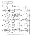
図2は、図1の本発明のマイクロコントローラの埋設フラッシュ・メモリ332に記憶されたファームウェアに含まれる手順のステップを示すフローチャートである。
図1および図2について説明すると、第一のステップ410においては、コンピュータ391の電源をオンにするか、リセットした直後に初期化が行われる。初期化の際に行われる動作は、コンピュータ業界では周知であるので、ここでは詳細な説明は省略する。初期化が終了すると、上記手順は次のステップ420へ行く。
【0036】
ステップ420においては、キーボード要求をキーボード381に送るべきかどうかのチェックが行われる。「イエス」である場合には、手順はステップ421へ行き、そこでシステム・インターフェース390を通して、ホスト・コンピュータ391からキーボード要求が取り出される。その後、手順はステップ422へ行き、そこでキーボード要求が、I/Oユニット317を通して、キーボード381に送られる。この手順が終了すると、手順はステップ420に戻り、ステップ420からのプログラム・ループが反復して行われる。ステップ420の結果が「ノー」である場合には、手順はステップ430へ行く。
【0037】
ステップ430においては、マウス要求をマウス382に送るべきかどうかのチェックが行われる。「イエス」である場合には、手順はステップ431へ行き、そこでシステム・インターフェース390を通して、ホスト・コンピュータ391からマウス要求が取り出される。その後、手順はステップ432へ行き、そこでマウス要求がI/Oユニット317を通して、マウス382に送られる。この手順が終了すると、手順はステップ420に戻り、ステップ420からのプログラム・ループが反復して行われる。ステップ430の結果が「ノー」である場合には、手順はステップ440へ行く。
【0038】
ステップ440においては、キーボード・データ信号が、キーボード381から入力中であるかどうかのチェックが行われる。「イエス」である場合には、手順はステップ441へ行き、そこでキーボード・データ信号が、I/Oユニット317を通して、キーボード381から受信される。その後、手順はステップ442へ行き、そこで受信キーボード・データ信号が、システム・インターフェース390を通して、ホスト・コンピュータ391に送られる。この手順が終了すると、手順はステップ420に戻り、ステップ420からのプログラム・ループが反復して行われる。ステップ440の結果が「ノー」である場合には、手順はステップ450へ行く。
【0039】
ステップ450においては、マウス・データ信号が、マウス382から入力中であるかどうかのチェックが行われる。「イエス」である場合には、手順はステップ451へ行き、そこでマウス・データ信号が、I/Oユニット317を通して、マウス382から受信される。その後、手順はステップ452へ行き、そこで受信マウス・データ信号が、システム・インターフェース390を通して、ホスト・コンピュータ391に送られる。この手順が終了すると、手順はステップ420に戻り、ステップ420からのプログラム・ループが反復して行われる。ステップ450の結果が「ノー」である場合には、手順はステップ460へ行く。
【0040】
ステップ460においては、プログラミング要求信号が、受信中であるかどうかのチェックが行われる。「イエス」である場合には、手順はステップ461へ行き、そこでフラッシュ・メモリ・ユニット332上の動作が、書込みモードに切り替えられる。その後、手順はステップ462に行き、そこで新しいプログラム・コードが、システム・インターフェース390を通して、ホスト・コンピュータ391から受信され、フラッシュ・メモリ・ユニット332の特定のアドレスに書き込まれる。書込み動作が終了すると、フラッシュ・メモリ・ユニット332に記憶された新しいプログラム・コードが、確認のために取り出され、ホスト・コンピュータ391に送られる。この手順が終了すると、手順はステップ420に戻り、ステップ420からのプログラム・ループが反復して行われる。ステップ460の結果が「ノー」である場合には、手順はステップ420へ戻る。
【0041】
つまり、本発明は、マイクロコントローラの埋設フラッシュ・メモリ・ユニットに記憶したファームウェアがチップ上で、容易にプログラムを行えるようにするオンチップ・プログラミング機能を持つ、新しいマイクロコントローラ・アーキテクチャを提供する。マイクロコントローラは、例えば、ホスト・コンピュータと、キーボードおよびマウスのような複数の周辺入力装置との間に接続しているデータ入力コントローラとして使用することができる。キーボード/マウス入力制御ファームウェアを更新する必要がある場合には、要求は、最初、ホスト・コンピュータからマイクロコントローラに送られ、それに応じて、マイクロコントローラのプログラミング制御ユニットが、マイクロコントローラの埋設フラッシュ・メモリへの新しいファームウェアのプログラミングを制御する。ホスト・コンピュータ側には、ユーザが、マイクロコントローラを取り外さないで、ソフトウェア制御によりプログラミングを行い、その後、プログラミングを行うための特殊なプログラミング装置を使用することができるように、装置ドライバを設置することができる。
【0042】
それ故、本発明のマイクロコントローラ・アーキテクチャは、従来技術より優れている。本発明を使用すれば、コンピュータのマザーボードから、マイクロコントローラ・ユニット全体を取り外さないで、ホスト・コンピュータからのソフトウェア制御によりプログラミングを行うことができる。それ故、従来技術と比較すると、プログラミング作業をより簡単にまたより容易に行うことができる。
例示としての好適な実施形態により本発明を説明してきたが、本発明の範囲は開示した実施形態に限定されないことを理解されたい。それどころか、種々の修正および類似の装置も本発明に含まれる。それ故、上記すべての修正および類似の装置がすべて本発明の範囲に含まれるように特許請求の範囲を広く解釈すべきである。
【図面の簡単な説明】
【図1】本発明のオンチップ・プログラミング機能を持つマイクロコントローラのアーキテクチャを示すブロック図である。
【図2】図1の本発明のマイクロコントローラの埋設フラッシュ・メモリに記憶された、ファームウェアに含まれる手順のステップを示すフローチャートである。
【図3】従来のマイクロコントローラの簡単なブロック図である。
【図4】図3の従来のマイクロコントローラのメモリに記憶されたファームウェアに含まれる手順のステップを示すフローチャートである。
【符号の説明】
300 マイクロコントローラ
305 主データ・バス
310 CPU
318 タイマー/カウンタ・ユニット
320 I/Oレジスタ・セット
332 フラッシュ・メモリ・ユニット
350 プログラミング制御ユニット
351 読出し/書込みコントローラ
352 マルチプレクサ・セット
353 ラッチ・セット
354 第四のマルチプレクサ[0001]
BACKGROUND OF THE INVENTION
The present invention relates to microcontroller architecture, and more particularly to embedded flash memory and microcontroller architecture with on-chip programming capability for flash memory.
[0002]
[Prior art]
<Cross-reference to related applications>
This application claims the benefit of priority of Taiwan Patent Application No. 87116528, Oct. 6, 1998, which is incorporated herein by reference in its entirety.
In a computer system such as an IBM compatible personal computer (PC), a dedicated microcontroller such as an Intel 8042 or 8742 microcontroller is used to control data input from a peripheral input device such as a keyboard or mouse. Has been. The 8042 unit is embedded with 2K x 8 ROM (read only memory), while the 8742 unit is an EEPROM (electrically erasable, programmable read only memory) or flash memory, Embedded with a 2K x 8 reprogrammable memory unit. These embedded memory units are used for storing firmware for controlling the input of data signals from a keyboard or mouse.
[0003]
Different types of keyboards, such as those designed for use in different countries, can be used with a personal computerDo Therefore, when using a new keyboard, the firmware for controlling the keyboard / mouse input preinstalled in the microcontroller must be replaced in order to realize compatibility. The 8042 embedded ROM cannot be reprogrammed. In the case of the 8742 unit, the embedded EEPROM or flash memory can be reprogrammed. In that case, the 8742 unit contained in the IC package is first removed from the circuit board inside the personal computer. After that, reprogramming by a special programmer and finally programming new firmware and then reattaching to the circuit board is cumbersome to reprogram. Therefore, reprogramming is inconvenient, cumbersome and costly. Figure3 And figure4 In the following, a conventional microcontroller architecture will be described.
[0004]
FIG. 3 is a simple block diagram illustrating the architecture of a conventional microcontroller for use with a personal computer to control keyboard / mouse input. This microcontroller is compatible with the Intel 8042 and 8742 specifications.
As shown in the figure, a conventional microcontroller architecture indicated by
[0005]
The
The I /
[0006]
In this
[0007]
Referring to FIG. 4 in conjunction with FIG. 3, in a
In
[0008]
In
[0009]
In
[0010]
In
[0011]
[Problems to be solved by the invention]
The above procedure is executed as firmware in the program
[0012]
Therefore, one object of the present invention is an embedded flash memory and a microcontroller architecture having an on-chip programming function for the flash memory, and the firmware stored in the embedded flash memory has been conventionally used. By providing a microcontroller architecture that allows programming on-chip without removing the microcontroller from the circuit board so that reprogramming is more convenient and easier than technology is there.
[0013]
[Means for Solving the Problems]
In accordance with the above and other objects of the present invention, a new microcontroller architecture with on-chip programming capability can be implemented. In operation, the microcontroller is connected to an external unit such as a PC through the system interface. The microcontroller architecture of the present invention includes a CPU, a main data bus, an I / O register set, a flash memory unit, a latch set, a multiplexer set, andRead / write controller Is provided.
[0014]
The main data bus is connected to the CPU. The I / O register set is connected between the CPU and the system interface. Flash memory unit is used to store program code. Enter A latch set whose power is connected to the I / O register set is used to receive new firmware programmed into the flash memory unit. The multiplexer set selectively connects the flash memory unit to the main data bus when operating in read mode, and connects the flash memory unit to the output of the latch set when in write mode.Read / write controller Controls the multiplexer set to connect the flash memory unit to the main data bus when operating in read mode and to connect the flash memory unit to the output of the latch set when in write mode A selection signal can be generated.Read / write controller The enable / disable signal to control the latch set in a way that also disables the latch set when operating in read mode and allows the latch set to operate when operating in write mode. Can be generated.
[0015]
When operating in read mode, the read / write controller switches the multiplexer set in such a way as to connect the main data bus to the flash memory and the program code stored in the flash memory unit. Are taken from the main data bus. When operating in write mode, the read / write controller switches the multiplexer set to connect the output of the latch set to the flash memory. New firmware received from the system interface through the I / O register set is first sent to the latch set, and then through the multiplexer set from the latch set to the flash memory unit. Allows new firmware to write to the flash memory unit.
[0016]
The new microcontroller architecture described above has on-chip programming capabilities that allow firmware stored in the embedded flash memory of the microcontroller to be easily programmed on the chip. By using the present invention, programming can be performed by software control from the host computer without removing the entire microcontroller from the computer motherboard. Therefore, compared with the prior art, the programming operation can be performed more easily and easily.
[0017]
The latch set includes a first latch, a second latch, and a third latch. The first latch has an output port connected to the multiplexer set and an input port connected to the main data bus. The first latch is used to latch the erase control code received from the system interface through the I / O register set. The second latch has an output port connected to the multiplexer set and an input port connected to the main data bus. The second latch is used to latch data signals received from the system interface through the I / O register set. The third latch has an output port connected to the multiplexer set and an input port connected to the main data bus. The third latch is used to latch the address signal received from the system interface through the I / O register set.
[0018]
The multiplexer set includes a first multiplexer, a second multiplexer, and a third multiplexer. Each multiplexer has a first port, a second port, a third port, and a selection control port. The first port is connected to the main data bus. The second port is connected to the output port of the corresponding latch of the latch set. The third port is connected to the flash memory unit. The selection control port is connected to receive a selection signal from the read / write controller. Further, each multiplexer can interconnect the third port and the first port when operating in read mode, and the third and second port when operating in write mode. Are controlled by a read / write controller to interconnect.
[0019]
The microcontroller architecture further comprises a fourth multiplexer. The fourth multiplexer has a first port, a second port, a third port, and a selection control port. The first port isThe first port of the first multiplexer, the first port of the second multiplexer, and the first port of the third multiplexer Connected to. The second port is connected to the second port of the second multiplexer. The third port isMain data bus and Connected to I / O register set. The selection control port is connected to receive a selection signal from the read / write controller. Similarly, the fourth multiplexer interconnects the third port and the first port when operating in read mode, and the third multiplexer and second port when operating in write mode. Controlled by the read / write controller to interconnect the two ports.
[0020]
The I / O register set includes a status register, an input register, and an output register. A status register connected between the main data bus and the system interface is used to temporarily store status data sent from the main data bus to the system interface. An input register connected between the main data bus and the system interface is used to temporarily store input data received from the system interface. An output register connected between the main data bus and the system interface is used to temporarily store output data sent from the main data bus to the system interface.
A more complete understanding of the present invention can be obtained by reading the following detailed description of the preferred embodiments with reference to the accompanying drawings, in which:
[0021]
DETAILED DESCRIPTION OF THE INVENTION
With reference to FIGS. 1 and 2, a preferred embodiment of the microcontroller architecture of the present invention will now be described.
Referring to FIG. 1, the microcontroller architecture of the present invention, indicated by
[0022]
The
[0023]
The I / O register set 320 is used to temporarily store I / O data and commands that travel between the
[0024]
A feature of the present invention is that it includes a
In this
[0025]
The
[0026]
The
[0027]
In the read mode, the read /
[0028]
In the write mode, the read /
[0029]
The
[0030]
The
[0031]
During normal operation, the
Stored in
[0032]
In the write mode, new firmware to program the
[0033]
If the select signal SA is in the second state, this signal interconnects its Y and B ports, thereby connecting the B port of the
If the result of the verification is that the new program code is correct, the
[0034]
Using this architecture,
[0035]
FIG. 2 is a flow chart showing the steps of the procedure contained in the firmware stored in the embedded
Referring to FIGS. 1 and 2, in the
[0036]
In
[0037]
In
[0038]
In step 440, a check is made as to whether a keyboard data signal is being input from the
[0039]
In
[0040]
In
[0041]
That is, the present invention provides a new microcontroller architecture with on-chip programming capability that allows firmware stored in the embedded flash memory unit of the microcontroller to be easily programmed on the chip. The microcontroller can be used as a data input controller connected between, for example, a host computer and a plurality of peripheral input devices such as a keyboard and a mouse. If the keyboard / mouse input control firmware needs to be updated, the request is first sent from the host computer to the microcontroller andIn In response, the microcontroller programming control unit controls the programming of new firmware into the microcontroller's embedded flash memory. On the host computer side, install a device driver so that the user can program by software control without removing the microcontroller and then use a special programming device for programming. Can do.
[0042]
Therefore, the microcontroller architecture of the present invention is superior to the prior art. By using the present invention, programming can be performed by software control from the host computer without removing the entire microcontroller unit from the motherboard of the computer. Therefore, the programming operation can be performed more easily and more easily as compared with the prior art.
While the invention has been described in terms of preferred embodiments by way of example, the scope of the invention is the disclosed embodiments.In It should be understood that it is not limited. On the contrary, various modifications and similar devices are also included in the invention. Therefore, the claims should be construed broadly so that all such modifications and similar devices are included within the scope of the invention.
[Brief description of the drawings]
FIG. 1 is a block diagram illustrating the architecture of a microcontroller with on-chip programming capability of the present invention.
2 is a flow chart showing the steps of the procedure included in the firmware stored in the embedded flash memory of the microcontroller of the present invention of FIG.
FIG. 3 is a simple block diagram of a conventional microcontroller.
4 is a flowchart showing the steps of a procedure included in firmware stored in the memory of the conventional microcontroller of FIG.
[Explanation of symbols]
300 microcontroller
305 Main data bus
310 CPU
318 Timer / Counter unit
320 I / O register set
332 Flash memory unit
350 Programming control unit
351 Read / write controller
352 Multiplexer set
353 Latch Set
354 Fourth multiplexer
Claims (8)
Translated fromJapaneseCPUと、
前記CPUに接続している主データ・バスと、
前記CPUと前記システム・インターフェースとの間に接続し、前記主データ・バスから前記システム・インターフェースへ送られる状態データを一時的に記憶する状態レジスタと、前記システム・インターフェースから受信する入力データを一時的に記憶する入力レジスタと、前記主データ・バスから前記システム・インターフェースへ送られる出力データを一時的に記憶する出力レジスタとを含むI/Oレジスタ・セットと、
プログラム・コードを記憶するためのフラッシュ・メモリ・ユニットと、
入力が前記主データ・バスを解して前記I/Oレジスタ・セットに接続し、前記フラッシュ・メモリ・ユニットにプログラムされる新しいファームウェアを受信するラッチ・セットと、
第一のマルチプレクサと、第二のマルチプレクサと、第三のマルチプレクサとを有するマルチプレクサ・セットと、
前記読出しモードで動作するときには前記主データ・バスを前記出力レジスタに接続し、書込みモードで動作するときには前記第二のマルチプレクサを前記出力レジスタに接続する第四のマルチプレクサと、
前記マルチプレクサ・セットを制御するための選択信号および前記ラッチ・セットを制御するためのイネーブル/ディスエーブル信号を発生する読出し/書込みコントローラとを備え、
前記読出し/書込みコントローラは、
前記読出しモードの場合には、前記選択信号を第一の論理状態に切り替えて、前記フラッシュ・メモリ・ユニットに記憶されているプログラム・コードを前記主データ・バスから取り出すことができるように前記主データ・バスを前記マルチプレクサ・セットを介して前記フラッシュ・メモリ・ユニットに接続し、前記イネーブル/ディスエーブル信号により前記ラッチ・セットを動作不能にし、
前記書込みモードの場合には、前記選択信号を第二の論理状態に切り替えて、前記I/Oレジスタ・セットを通して前記システム・インターフェースから受信した前記新しいファームウェアを、最初、ラッチ・セットに送り、その後で、マルチプレクサ・セットを通してラッチ・セットからフラッシュ・メモリ・ユニットに送り、それにより、前記新しいファームウェアを前記フラッシュ・メモリ・ユニットに書き込むことができるように前記ラッチ・セットの出力を前記フラッシュ・メモリ・ユニットに接続し、前記イネーブル/ディスエーブル信号により前記ラッチ・セットを動作可能にすることを特徴とするマイクロコントローラ。A microcontroller with on-chip programming function connected to an external device through a system interface,
CPU,
A main data bus connected to the CPU;
A status register connected between the CPU and the system interface, temporarily storing status data sent from the main data bus to the system interface, and input data received from the system interface An I / O register set including an input register for storing the output and an output register for temporarily storing output data sent from the main data bus to the system interface;
A flash memory unit for storing program codes;
A latch set whose inputs connect to the I / O register set via the main data bus and receive new firmware programmed into the flash memory unit;
A multiplexer set having a first multiplexer, a second multiplexer, and a third multiplexer;
Connect thepre SL main databus when operating in the read mode to the outputregister, and a fourth multiplexer when operating inwriting inclusive mode for connecting the second multiplexer to the output register,
And a read / write controller for generating an enable / disable signal for controlling the selection signals and the latchset for controlling said multiplexer set,
The read / write controller is
In the read mode, the selection signalisswitched to a first logic state so that the program code stored in the flash memory unit can be retrieved from the main data bus. A data bus is connectedto the flash memory unit via themultiplexer set , the enable / disable signal disables the latch set;
In the write mode, the selection signalisswitched to a second logic state, and the new firmware received from the system interface through the I / O register set is first sent to the latch set and then The output of the latch set to the flash memory unit so that the new firmware can be written to the flash memory unit through the multiplexer set to the flash memory unit. A microcontroller connectedto a unit and enabling the latch set by the enable / disable signal.
前記第一のラッチは、前記I/Oレジスタ・セットを通して前記システム・インターフェースから受信した消去制御コードをラッチし、
前記第二のラッチは、前記I/Oレジスタ・セットを通して前記システム・インターフェースから受信したデータ信号をラッチし、
前記第三のラッチは、前記I/Oレジスタ・セットを通して前記システム・インターフェースから受信したアドレス信号をラッチすることを特徴とするマイクロコントローラ。2. The microcontroller of claim 1, wherein the latch set comprises a first latch having an output port connected to the multiplexer set and an input port connected to the main data bus. Including a second latch, and a third latch,
The first latch latches an erase control code received from the system interface through the I / O register set;
The second latch latches a data signal received from the system interface through the I / O register set;
The microcontroller according to claim 3, wherein the third latch latches an address signal received from the system interface through the I / O register set.
前記第一のマルチプレクサは、前記第一のポートが前記第四のマルチプレクサを介して前記主データ・バスに接続し、前記第二のポートが前記ラッチ・セットの前記第一のラッチの出力ポートに接続し、前記第三のポートが前記フラッシュ・メモリ・ユニットに接続し、前記選択制御ポートが前記読出し/書込みコントローラに接続していて、前記読出し/書込みコントローラから受信する前記選択信号が第一の論理状態である場合には前記読出しモードで動作して前記第三のポートと前記第一のポートを相互接続し、また前記選択信号が第二の論理状態である場合には前記書込みモードで動作して前記第三のポートと前記第二のポートを相互接続するように、前記読出し/書込みコントローラにより制御され、
前記第二のマルチプレクサは、前記第一のポートが前記第四のマルチプレクサを介して前記主データ・バスに接続し、前記第二のポートが前記ラッチ・セットの前記第二のラッチの出力ポートに接続し、前記第三のポートが前記フラッシュ・メモリ・ユニットに接続し、前記選択制御ポートが前記読出し/書込みコントローラに接続していて、前記読出し/書込みコントローラから受信する前記選択信号が第一の論理状態である場合には前記読出しモードで動作して前記第三のポートと前記第一のポートを相互接続し、また前記選択信号が第二の論理状態である場合には前記書込みモードで動作して前記第三のポートと前記第二のポートを相互接続するように、前記読出し/書込みコントローラにより制御され、
前記第三のマルチプレクサは、前記第一のポートが前記第四のマルチプレクサを介して前記主データ・バスに接続し、前記第二のポートが前記ラッチ・セットの前記第三のラッチの出力ポートに接続し、前記第三のポートが前記フラッシュ・メモリ・ユニットに接続し、前記選択制御ポートが前記読出し/書込みコントローラに接続していて、前記読出し/書込みコントローラから受信する前記選択信号が第一の論理状態である場合には前記読出しモードで動作して前記第三のポートと前記第一のポートを相互接続し、また前記選択信号が第二の論理状態である場合には前記書込みモードで動作して前記第三のポートと前記第二のポートを相互接続するように、前記読出し/書込みコントローラにより制御されることを特徴とするマイクロコントローラ。3. The microcontroller of claim 2, wherein the first multiplexer, the second multiplexer, and the third multiplexer of the multiplexer set are each a first port, a second port, a third port, And have a select control port,
The first multiplexer has the first port connected to the main data bus through the fourth multiplexer, and the second port to the output port of the first latch of the latch set. The third port is connected to the flash memory unit, the selection control port is connected to the read / write controller, and the selection signal received from the read / write controller is a first Operates in the read mode when in a logic state to interconnect the third port and the first port, and operates in the write mode when the selection signal is in a second logic state Controlled by the read / write controller to interconnect the third port and the second port;
In the second multiplexer, the first port is connected to the main data bus via the fourth multiplexer, and the second port is an output port of the second latch of the latch set. The third port is connected to the flash memory unit, the selection control port is connected to the read / write controller, and the selection signal received from the read / write controller is a first Operates in the read mode when in a logic state to interconnect the third port and the first port, and operates in the write mode when the selection signal is in a second logic state Controlled by the read / write controller to interconnect the third port and the second port;
In the third multiplexer, the first port is connected to the main data bus through the fourth multiplexer, and the second port is an output port of the third latch of the latch set. The third port is connected to the flash memory unit, the selection control port is connected to the read / write controller, and the selection signal received from the read / write controller is a first Operates in the read mode when in a logic state to interconnect the third port and the first port, and operates in the write mode when the selection signal is in a second logic state The microcontroller is controlled by the read / write controller to interconnect the third port and the second port. Controller.
前記第四のマルチプレクサは、第一のポート、第二のポート、第三のポート、および選択制御ポートを有し、前記第一のポートが前記第一のマルチプレクサの第一のポート、第二のマルチプレクサの第一のポート、および第三のマルチプレクサの第一のポートに接続し、前記第二のポートが前記第二のマルチプレクサの第二のポートに接続し、前記第三のポートが前記主データ・バスおよび前記I/Oレジスタ・セットに接続し、前記選択制御ポートが前記読出し/書込みコントローラに接続していて、前記読出し/書込みコントローラから受信する前記選択信号が第一の論理状態である場合には前記読出しモードで動作して前記第三のポートと前記第一のポートを相互接続し、また前記選択信号が第二の論理状態である場合には前記書込みモードで動作して前記第三のポートと前記第二のポートを相互接続するように、前記読出し/書込みコントローラにより制御されることを特徴とするマイクロコントローラ。The microcontroller of claim 3,
The fourth multiplexer has a first port, a second port, a third port, and a selection control port, wherein the first port is a first port of the first multiplexer, a second port A first port of a multiplexer and a first port of a third multiplexer; the second port is connected to a second port of the second multiplexer; and the third port is the main data When connected to the bus and the I / O register set, the selection control port is connected to the read / write controller, and the selection signal received from the read / write controller is in the first logic state Operates in the read mode to interconnect the third port and the first port, and the write signal when the select signal is in the second logic state. Over the second port and the third port operates to interconnect with de, microcontroller, characterized in that it is controlled by the read / write controller.
前記CPUに接続している主データ・バスと、
前記主データ・バスとシステム・インターフェースとの間に接続し、前記主データ・バスから前記システム・インターフェースに送られる状態データを一時的に記憶する状態レジスタと、前記システム・インターフェースから受信する入力データを一時的に記憶する入力レジスタと、前記主データ・バスから前記システム・インターフェースへ送られる出力データを一時的に記憶する出力レジスタとを含むI/Oレジスタ・セットと、
前記I/Oレジスタ・セットと外部装置との間に接続しているシステム・インターフェースと、
前記フラッシュ・メモリ・ユニットのプログラミングを制御するためのプログラム・コードを記憶するフラッシュ・メモリ・ユニットとを有するマイクロコントローラ上で使用するプログラミング制御ユニットであって、
前記プログラミング制御ユニットが、
入力が前記主データ・バスを介して前記I/Oレジスタ・セットに接続し、前記フラッシュ・メモリ・ユニットにプログラムされる新しいファームウェアを受信するラッチ・セットと、
第一のマルチプレクサと、第二のマルチプレクサと、第三のマルチプレクサとを有するマルチプレクサ・セットと、
前記読出しモードで動作するときには前記主データ・バスを前記出力レジスタに接続し、書込みモードで動作するときには前記第二のマルチプレクサを前記出力レジスタに接続する第四のマルチプレクサと、
前記マルチプレクサ・セットを制御するための選択信号および前記ラッチ・セットを制御するためのイネーブル/ディスエーブル信号を発生する読出し/書込みコントローラとを備え、
前記読出し/書込みコントローラは、
前記読出しモードの場合には、前記選択信号を第一の論理状態に切り替えて、前記フラッシュ・メモリ・ユニットに記憶されている前記プログラム・コードを前記主データ・バスから取り出すことができるように前記主データ・バスを前記マルチプレクサ・セットを介して前記フラッシュ・メモリ・ユニットに接続し、前記イネーブル/ディスエーブル信号により前記ラッチ・セットを動作不能にし、
前記書込みモードの場合には、前記選択信号を第二の論理状態に切り替えて、前記I/Oレジスタ・セットを通して前記システム・インターフェースから受信した前記新しいファームウェアを、最初、前記ラッチ・セットに送り、その後で、前記マルチプレクサ・セットを通してラッチ・セットからフラッシュ・メモリ・ユニットに送り、それにより、前記新しいファームウェアを前記フラッシュ・メモリ・ユニットに書き込むことができるように、前記ラッチ・セットの出力を前記フラッシュ・メモリ・ユニットに接続し、前記イネーブル/ディスエーブル信号により前記ラッチ・セットの動作を可能にすることを特徴とするプログラミング制御ユニット。CPU,
A main data bus connected to the CPU;
A status register connected between the main data bus and the system interface for temporarily storing status data sent from the main data bus to the system interface; and input data received from the system interface An I / O register set that includes an input register that temporarily stores data and an output register that temporarily stores output data sent from the main data bus to the system interface;
A system interface connected between the I / O register set and an external device;
A programming control unit for use on a microcontroller having a flash memory unit storing program code for controlling programming of said flash memory unit,
The programming control unit is
A latch set whose inputs connect to the I / O register set via the main data bus and receive new firmware programmed into the flash memory unit;
A multiplexer set having a first multiplexer, a second multiplexer, and a third multiplexer;
When operating in the read mode is connected to the main data bus to said outputregister, and a fourth multiplexer when operating inwriting inclusive mode for connecting the second multiplexer to the output register,
And a read / write controller for generating an enable / disable signal for controlling the selection signals and the latchset for controlling said multiplexer set,
The read / write controller is
In the read mode, the selection signalisswitched to a first logic state so that the program code stored in the flash memory unit can be retrieved from the main data bus. A main data bus is connectedto the flash memory unit via themultiplexer set, and the latch set is disabled by the enable / disable signal;
In the case of the write mode, the selection signalisswitched to a second logic state, and the new firmware received from the system interface through the I / O register set is first sent to the latch set; Thereafter, the latch set output is sent to the flash memory unit through the multiplexer set so that the new firmware can be written to the flash memory unit. A programming control unit connectedto a memory unit and enabling operation of the latch set by the enable / disable signal.
前記第一のラッチは、前記I/Oレジスタ・セットを通して前記システム・インターフェースから受信した消去制御コードをラッチし、
前記第二のラッチは、前記I/Oレジスタ・セットを通して前記システム・インターフェースから受信したデータ信号をラッチし、
前記第三のラッチは、前記I/Oレジスタ・セットを通して前記システム・インターフェースから受信したアドレス信号をラッチすることを特徴とするプログラミング制御ユニット。6. A programming control unit according to claim 5, wherein the latch set comprises a first latch having an output port connected to the multiplexer set and an input port connected to the main data bus. Including a second latch and a third latch;
The first latch latches an erase control code received from the system interface through the I / O register set;
The second latch latches a data signal received from the system interface through the I / O register set;
The programming control unit, wherein the third latch latches an address signal received from the system interface through the I / O register set.
前記第一のマルチプレクサは、前記第一のポートが前記主データ・バスに接続し、前記第二のポートが前記ラッチ・セットの前記第一のラッチの出力ポートに接続し、前記第三のポートが前記フラッシュ・メモリ・ユニットに接続し、前記選択制御ポートが前記読出し/書込みコントローラに接続していて、前記読出し/書込みコントローラから受信する前記選択信号が第一の論理状態である場合には前記読出しモードで動作して前記第三のポートと前記第一のポートを相互接続し、また前記選択信号が第二の論理状態である場合には前記書込みモードで動作して前記第三のポートと前記第二のポートを相互接続するように、前記読出し/書込みコントローラにより制御され、
前記第二のマルチプレクサは、前記第一のポートが前記主データ・バスに接続し、前記第二のポートが前記ラッチ・セットの前記第二のラッチの出力ポートに接続し、前記第三のポートが前記フラッシュ・メモリ・ユニットに接続し、前記選択制御ポートが前記読出し/書込みコントローラに接続していて、前記読出し/書込みコントローラから受信する前記選択信号が第一の論理状態である場合には前記読出しモードで動作して前記第三のポートと前記第一のポートを相互接続し、また前記選択信号が第二の論理状態である場合には前記書込みモードで動作して前記第三のポートと前記第二のポートを相互接続するように、前記読出し/書込みコントローラにより制御され、
前記第三のマルチプレクサは、前記第一のポートが前記主データ・バスに接続し、前記第二のポートが前記ラッチ・セットの前記第三のラッチの出力ポートに接続し、前記第三のポートが前記フラッシュ・メモリ・ユニットに接続し、前記選択制御ポートが前記読出し/書込みコントローラに接続していて、前記読出し/書込みコントローラから受信する前記選択信号が第一の論理状態である場合には前記読出しモードで動作して前記第三のポートと前記第一のポートを相互接続し、また前記選択信号が第二の論理状態である場合には前記書込みモードで動作して前記第三のポートと前記第二のポートを相互接続するように、前記読出し/書込みコントローラにより制御されることを特徴とするプログラミング制御ユニット。7. The programming control unit according to claim 6, wherein the first multiplexer, the second multiplexer, and the third multiplexer of the multiplexer set are respectively a first port, a second port, and a third port. And having a selection control port,
The first multiplexer has the first port connected to the main data bus, the second port connected to the output port of the first latch of the latch set, and the third port. Is connected to the flash memory unit, the selection control port is connected to the read / write controller, and the selection signal received from the read / write controller is in a first logic state, Operate in read mode to interconnect the third port and the first port, and operate in the write mode if the select signal is in the second logic state Controlled by the read / write controller to interconnect the second ports;
The second multiplexer has the first port connected to the main data bus, the second port connected to the output port of the second latch of the latch set, and the third port. Is connected to the flash memory unit, the selection control port is connected to the read / write controller, and the selection signal received from the read / write controller is in a first logic state, Operate in read mode to interconnect the third port and the first port, and operate in the write mode if the select signal is in the second logic state Controlled by the read / write controller to interconnect the second ports;
The third multiplexer has the first port connected to the main data bus, the second port connected to the output port of the third latch of the latch set, and the third port. Is connected to the flash memory unit, the selection control port is connected to the read / write controller, and the selection signal received from the read / write controller is in a first logic state, Operate in read mode to interconnect the third port and the first port, and operate in the write mode if the select signal is in the second logic state A programming control unit controlled by the read / write controller to interconnect the second ports.
前記第四のマルチプレクサは、第一のポート、第二のポート、第三のポート、および選択制御ポートを有し、前記第一のポートが前記第一のマルチプレクサの第一のポート、第二のマルチプレクサの第一のポート、および第三のマルチプレクサの第一のポートに接続し、前記第二のポートが前記第二のマルチプレクサの第二のポートに接続し、前記第三のポートが前記主データ・バスおよび前記I/Oレジスタ・セットに接続し、前記選択制御ポートが前記読出し/書込みコントローラに接続していて、前記読出し/書込みコントローラから受信する前記選択信号が第一の論理状態である場合には前記読出しモードで動作して前記第三のポートと前記第一のポートを相互接続し、また前記選択信号が第二の論理状態である場合には前記書込みモードで動作して前記第三のポートと前記第二のポートを相互接続するように、前記読出し/書込みコントローラにより制御されることを特徴とするプログラミング制御ユニット。The programming control unit according to claim 7,
The fourth multiplexer has a first port, a second port, a third port, and a selection control port, wherein the first port is a first port of the first multiplexer, a second port A first port of a multiplexer and a first port of a third multiplexer; the second port is connected to a second port of the second multiplexer; and the third port is the main data When connected to the bus and the I / O register set, the selection control port is connected to the read / write controller, and the selection signal received from the read / write controller is in the first logic state Operates in the read mode to interconnect the third port and the first port, and the write signal when the select signal is in the second logic state. The second port and the third port operates to interconnect with over de, programming the control unit, characterized in that it is controlled by the read / write controller.
Applications Claiming Priority (2)
| Application Number | Priority Date | Filing Date | Title |
|---|---|---|---|
| TW087116528ATW374883B (en) | 1998-10-06 | 1998-10-06 | Microcontroller featuring engraving functions on chips |
| TW87116528 | 1998-10-06 |
Publications (2)
| Publication Number | Publication Date |
|---|---|
| JP2000112745A JP2000112745A (en) | 2000-04-21 |
| JP4042940B2true JP4042940B2 (en) | 2008-02-06 |
Family
ID=21631564
Family Applications (1)
| Application Number | Title | Priority Date | Filing Date |
|---|---|---|---|
| JP04211799AExpired - Fee RelatedJP4042940B2 (en) | 1998-10-06 | 1999-02-19 | Microcontroller with on-chip programming function |
Country Status (2)
| Country | Link |
|---|---|
| JP (1) | JP4042940B2 (en) |
| TW (1) | TW374883B (en) |
Families Citing this family (3)
| Publication number | Priority date | Publication date | Assignee | Title |
|---|---|---|---|---|
| JP2005038382A (en)* | 2003-06-26 | 2005-02-10 | Sanyo Electric Co Ltd | Control device and data writing method |
| TWI384237B (en)* | 2009-04-02 | 2013-02-01 | King Yuan Electronics Co Ltd | Chip burn-in machine with group testing |
| TWI780382B (en)* | 2019-12-05 | 2022-10-11 | 新唐科技股份有限公司 | Microcontroller updating system and method |
- 1998
- 1998-10-06TWTW087116528Apatent/TW374883B/ennot_activeIP Right Cessation
- 1999
- 1999-02-19JPJP04211799Apatent/JP4042940B2/ennot_activeExpired - Fee Related
Also Published As
| Publication number | Publication date |
|---|---|
| JP2000112745A (en) | 2000-04-21 |
| TW374883B (en) | 1999-11-21 |
Similar Documents
| Publication | Publication Date | Title |
|---|---|---|
| KR100375217B1 (en) | Microcontroller incorporating an electrically rewritable non-volatile memory | |
| US6009496A (en) | Microcontroller with programmable embedded flash memory | |
| EP1938200B1 (en) | Initialization of flash storage via an embedded controller | |
| US20030131185A1 (en) | Flash memory command abstraction | |
| US20100325467A1 (en) | Memory system and controller | |
| US7480905B2 (en) | Interface device, and method and computer readable product for updating firmware in the interface device | |
| JPH06325185A (en) | Integrated circuit with microprocessor, memory and peripheral devices configurable internally | |
| JP3173407B2 (en) | Microcomputer with built-in flash EEPROM | |
| US7046536B2 (en) | Programable identification circuitry | |
| JP4042940B2 (en) | Microcontroller with on-chip programming function | |
| JP2971267B2 (en) | Personal computer using flash memory as BIOS-ROM | |
| JP2004021867A (en) | Information processing system | |
| CN101432674A (en) | Methods of inter-integrated circuit addressing and devices for performing the same | |
| JP2008027326A (en) | System controller, flash memory system having system controller, and control method of flash memory module | |
| JPS63106996A (en) | Semiconductor integrated circuit device | |
| JP4958201B2 (en) | Microcomputer | |
| JP3635996B2 (en) | Information processing system | |
| JP4083474B2 (en) | MEMORY DEVICE CONTROL METHOD, PROGRAM THEREOF, AND RECORDING MEDIUM | |
| KR20000033437A (en) | Apparatus for implementing function of bootstrap loader | |
| KR100290280B1 (en) | Microcontroller with Programmable Flash Memory | |
| JPH10143434A (en) | Semiconductor integrated circuit | |
| JP2000029679A (en) | Personal computer using flash memory as BIOS-ROM | |
| JP2000259448A (en) | Program debug device | |
| JP4328790B2 (en) | Semiconductor integrated circuit | |
| JPH0283678A (en) | How to develop a data processing system |
Legal Events
| Date | Code | Title | Description |
|---|---|---|---|
| A621 | Written request for application examination | Free format text:JAPANESE INTERMEDIATE CODE: A621 Effective date:20040517 | |
| A131 | Notification of reasons for refusal | Free format text:JAPANESE INTERMEDIATE CODE: A131 Effective date:20060725 | |
| A601 | Written request for extension of time | Free format text:JAPANESE INTERMEDIATE CODE: A601 Effective date:20061025 | |
| A602 | Written permission of extension of time | Free format text:JAPANESE INTERMEDIATE CODE: A602 Effective date:20061101 | |
| A521 | Written amendment | Free format text:JAPANESE INTERMEDIATE CODE: A523 Effective date:20070122 | |
| A131 | Notification of reasons for refusal | Free format text:JAPANESE INTERMEDIATE CODE: A131 Effective date:20070320 | |
| A601 | Written request for extension of time | Free format text:JAPANESE INTERMEDIATE CODE: A601 Effective date:20070620 | |
| A602 | Written permission of extension of time | Free format text:JAPANESE INTERMEDIATE CODE: A602 Effective date:20070625 | |
| A521 | Written amendment | Free format text:JAPANESE INTERMEDIATE CODE: A523 Effective date:20070704 | |
| TRDD | Decision of grant or rejection written | ||
| A01 | Written decision to grant a patent or to grant a registration (utility model) | Free format text:JAPANESE INTERMEDIATE CODE: A01 Effective date:20071030 | |
| A61 | First payment of annual fees (during grant procedure) | Free format text:JAPANESE INTERMEDIATE CODE: A61 Effective date:20071109 | |
| R150 | Certificate of patent or registration of utility model | Free format text:JAPANESE INTERMEDIATE CODE: R150 | |
| FPAY | Renewal fee payment (event date is renewal date of database) | Free format text:PAYMENT UNTIL: 20101122 Year of fee payment:3 | |
| FPAY | Renewal fee payment (event date is renewal date of database) | Free format text:PAYMENT UNTIL: 20111122 Year of fee payment:4 | |
| FPAY | Renewal fee payment (event date is renewal date of database) | Free format text:PAYMENT UNTIL: 20121122 Year of fee payment:5 | |
| FPAY | Renewal fee payment (event date is renewal date of database) | Free format text:PAYMENT UNTIL: 20121122 Year of fee payment:5 | |
| FPAY | Renewal fee payment (event date is renewal date of database) | Free format text:PAYMENT UNTIL: 20131122 Year of fee payment:6 | |
| R250 | Receipt of annual fees | Free format text:JAPANESE INTERMEDIATE CODE: R250 | |
| R250 | Receipt of annual fees | Free format text:JAPANESE INTERMEDIATE CODE: R250 | |
| R250 | Receipt of annual fees | Free format text:JAPANESE INTERMEDIATE CODE: R250 | |
| R250 | Receipt of annual fees | Free format text:JAPANESE INTERMEDIATE CODE: R250 | |
| R250 | Receipt of annual fees | Free format text:JAPANESE INTERMEDIATE CODE: R250 | |
| LAPS | Cancellation because of no payment of annual fees |