JP4040819B2 - Wafer dividing method and semiconductor device manufacturing method - Google Patents
Wafer dividing method and semiconductor device manufacturing methodDownload PDFInfo
- Publication number
- JP4040819B2 JP4040819B2JP2000013231AJP2000013231AJP4040819B2JP 4040819 B2JP4040819 B2JP 4040819B2JP 2000013231 AJP2000013231 AJP 2000013231AJP 2000013231 AJP2000013231 AJP 2000013231AJP 4040819 B2JP4040819 B2JP 4040819B2
- Authority
- JP
- Japan
- Prior art keywords
- wafer
- chip
- grinding
- polishing
- groove
- Prior art date
- Legal status (The legal status is an assumption and is not a legal conclusion. Google has not performed a legal analysis and makes no representation as to the accuracy of the status listed.)
- Expired - Lifetime
Links
Images


Landscapes
- Mechanical Treatment Of Semiconductor (AREA)
- Dicing (AREA)
- Weting (AREA)
Description
Translated fromJapanese【0001】
【発明の属する技術分野】
この発明はウェーハの分割方法及び半導体装置の製造方法に関し、更に詳しくは、ウェーハ上に形成された半導体素子を個々のチップに切断分離し、外囲器に封止する工程に関し、外囲器の小型薄厚化やウェーハの大口径化時に好適なものである。
【0002】
【従来の技術】
半導体装置の製造工程は、ウェーハ(半導体基板)上に種々の半導体素子のパターンを形成する工程と、ウェーハ上に形成された半導体素子を個々のチップに切断分離し、外囲器に封止する工程とに大別できる。近年、製造コストの低減を図るためにウェーハの大口径化が推進されるとともに、実装密度を高めるために外囲器の小型薄厚化が望まれている。従来は、薄厚化した外囲器に封止するために、ウェーハを個々のチップに切断分離するのに先立って、ウェーハのパターン形成面(主表面)の反対側の面(ウェーハの裏面)を砥石による研削及び遊離砥粒による研磨等により除去して薄くし、その後ダイシングして切断分離している。研削時には、ウェーハのパターン形成面に粘着性のシートを貼り付けたり、レジスト等を塗布することによって保護している。この後、上記ウェーハの主表面に形成された切断分離(ダイシング)ライン領域に溝を形成する。この溝を形成する際には、ダイヤモンドスクライバー、ダイヤモンドブレード、あるいはレーザースクライバー等を用いている。上記ダイシング工程には、ウェーハ単体でこのウェーハの厚さの1/2までダイシングまたはウェーハが30μm程度残る状態までダイシングを行うハーフカット法、ウェーハの裏面に粘着性のシートを貼り付けて同様にダイシングするハーフカット法、粘着性のシートを20〜30μm程度まで切り込み、ウェーハ厚全てを切断するフルカット法等が用いられる。上記ハーフカット法は、分割作業が必要とされ、ウェーハ単体の場合にはウェーハを柔軟性のあるフィルム等に挟み、ローラー等で外力を加えて割って分割する。シートに貼り付けた場合には、テープ越しにローラーその他で外力を加え分割する。分割されたチップは、ダイボンディング装置に設けられているピックアップニードルによってシート裏面を突き上げ、このシートを貫通してチップ裏面にニードル(針)を直接接触させ、更に持ち上げてチップをシートから引き離す。引き離されたチップは、コレットと呼ばれるツールでチップ表面を吸着し、リードフレームのアイランドにマウントした後、ワイヤボンディングを行ってチップの各パッドとリードフレームのインナーリード部とを電気的に接続し、外囲器に封止している。上記チップのアイランドへのマウント方法としては、アイランドへ導電性ペーストを予め塗布しておく方法、金−シリコンの共晶を利用してマウントする方法、及びウェーハの裏面に金属の薄膜を蒸着し、半田を用いてマウントする方法等がある。
【0003】
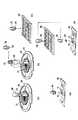
図22乃至図28はそれぞれ、上述したような従来のウェーハの分割方法及び半導体装置の製造方法の詳細な例について説明するためのもので、図22はウェーハに表面保護テープを貼り付ける工程、図23はウェーハの裏面の研削及び研磨工程、図24は表面保護テープを剥がす工程、図25(a),(b)はウェーハを固定用シートに固着する工程、図26はウェーハのダイシング工程、図27は分離したチップをピックアップする工程、及び図28はダイボンディング工程をそれぞれ示している。
【0004】
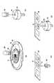
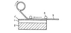
まず、図22に示すように、ウェーハ1の裏面をチャックテーブル2上に固定し、貼り付けローラー4を回転させながら図示矢印方向に移動させて、保護テープ3をウェーハ1のパターン形成面(ウェーハ1の主表面)1’に貼り付ける。このウェーハ1中には、パターン形成面1’側に各種の半導体素子が形成されている。次に、図23に示すように、上記保護テープ3を貼り付けたパターン形成面1’を下にしてチャックテーブル5に固定し、ウェーハ1の裏面を研削用砥石6で所定の厚さ(完成時の最終的なチップ厚)まで研削及び研磨する。その後、図24に示すように、保護テープ3に保護テープを剥がすためのテープ7を貼り付け、パターン形成面1’から保護テープ3を剥離する。次に、図25(a)に示すようなフラットリング8をウェーハの固定用シート9に固着してシート9の弛みや皺などの発生を防止した状態で、図25(b)に示す如くフラットリング8の開口内のシート9上にウェーハ1を固着する。そして、上記ウェーハ1を固着したシート9とフラットリング8をダイシング用のチャックテーブル10に固定し、ダイシング用ブレード11でダイシング(フルカット)し、個々のチップ12に切断分離する(図26参照)。次に、図27に示すように、シート9の下方からピックアップニードル13をシート9を貫通させて、チップ12の裏面に当てて上方に押圧することにより個々のチップ12をシート9から剥離し、図28に示すようにリードフレームのアイランド14に導電性ペースト等のダイボンディング用接着剤を用いてマウントする。その後、図示しないがリードフレームのインナーリード部とチップ12の各パッドとをワイヤボンディングし、樹脂製やセラミック製の外囲器に封止して半導体装置を完成する。
【0005】
しかしながら、上記のようなウェーハの分割方法及び半導体装置の製造方法では、下記(a)〜(c)に示すような問題がある。
【0006】
(a)薄厚研削時にウェーハが割れ易い。保護テープを貼り付けて研削を行っても、研削時の歪みによりウェーハが反ってしまい、このために研削装置内での搬送時に引っ掛かったりして破損する。また、ウェーハが薄くなったり大口径化されるに従いウェーハの強度が低下するため、現状のようにウェーハを薄くした後、ウェーハ単体を搬送して種々の処理を施す方法では破損する確率が高くなる。例えば、ウェーハが400μmの厚さでは1.6Kgf/mm2程度まで耐えられるが、厚さが200μmになると0.4Kgf/mm2と1/4にまで低下する。
【0007】
(b)パターン形成面の保護とダイシング時のウェーハ保持用として二枚のシートを使用するため、これらの貼り付け、剥離、貼り付けと工程がそれぞれ必要となり、材料費が高くなり製造工程も増加する。
【0008】
(c)ダイシングを行った場合、ウェーハの裏面側のチッピングが大きくなり、チップの抗折強度の低下を招く。しかも、従来は種々の特性モニター用のトランジスタ、抵抗及びコンデンサー等(これらをTEG:Test Element Groupと称する)をチップ内に配置していたが、近年は高集積化を図るためにダイシングライン上に配置するようになった。周知の通り、これらの素子は酸化膜、アルミニウム等で構成されており、ダイヤモンドブレードを用いてダイシングを行う際に、砥石の目詰まりを起こし易く、切れ味を阻害する材料である。このため、ダイシングライン上にTEGが配置されている場合には、ウェーハの裏面側のチッピングが更に大きくなる。一般に半導体基板として使用されている材料はシリコンやGaAs等の脆性材であるために、チッピングやクラック等が存在すると抗折強度の低下を招きやすい。
【0009】
【発明が解決しようとする課題】
上記のように従来のウェーハの分割方法及び半導体装置の製造方法は、薄厚研削時や搬送時にウェーハが割れやすいという問題があった。また、パターン形成面の保護とウェーハの保持のために二枚のシートを必要とするため、材料費が高くなり製造工程も増加するという問題があった。更に、ダイシングを行った場合、ウェーハの裏面側のチッピングが大きくなり、チップの抗折応力の低下を招くという問題があった。
【0010】
この発明は上記のような事情に鑑みてなされたもので、その目的とするところは、薄厚研削時や搬送時のウェーハの割れを抑制できるウェーハの分割方法及び半導体装置の製造方法を提供することにある。
【0011】
また、この発明の他の目的は、製造工程とコストの削減が図れるウェーハの分割方法及び半導体装置の製造方法を提供することにある。
【0012】
この発明の更に他の目的は、ウェーハの裏面側のチッピングを小さくでき、チップの抗折応力の低下を抑制できるウェーハの分割方法及び半導体装置の製造方法を提供することにある。
【0013】
【課題を解決するための手段】
この発明のウェーハの分割方法は、半導体素子が形成されたウェーハのダイシングラインに沿って、先端部に曲面を有するダイシング用ブレードを用いて、前記半導体素子の形成面側から完成時のチップの厚さよりも深く、且つ底部に曲面を有する溝を形成する工程と、前記ウェーハにおける前記半導体素子の形成面上に保持部材を貼り付ける工程と、前記ウェーハの裏面を研削及び研磨して、ウェーハを個々のチップに分離し、研削及び研磨によってウェーハが個々のチップに分割された後も研削及び研磨を続け、前記完成時のチップの厚さにする工程とを具備し、前記ウェーハの研削及び研磨面が前記溝の底部に達してから、完成時のチップ厚になるまでの研削及び研磨量と、前記溝の底部における曲面を有する領域の深さとの比が0.3以上であることを特徴としている。
【0015】
更に、この発明のウェーハの分割方法は、半導体素子が形成されたウェーハのチップ分割ラインに沿ってエッチングすることにより、前記半導体素子の形成面側から完成時のチップの厚さよりも深く、且つ底部に曲面を有する溝を形成する工程と、前記ウェーハにおける前記半導体素子の形成面上に保持部材を貼り付ける工程と、前記ウェーハの裏面を研削及び研磨して、ウェーハを個々のチップに分離し、研削及び研磨によってウェーハが個々のチップに分割された後も研削及び研磨を続け、前記完成時のチップの厚さにする工程とを具備し、前記ウェーハの研削及び研磨面が前記溝の底部に達してから、完成時のチップ厚になるまでの研削及び研磨量と、前記溝の底部における曲面を有する領域の深さとの比が0.3以上であることを特徴としている。
【0016】
そして、下記(A)〜(E)のような特徴を備えている。
【0017】
(A)前記溝の深さは、前記完成時のチップの厚さよりも少なくとも5μm深い。
【0018】
(B)前記溝の深さは、前記完成時のチップの厚さよりも5μm乃至60μm深い。
【0019】
(C)前記保持部材は、粘着材付きテープ、ワックス、吸着パッド、熱圧着シート、粘着材を塗布した基板、及び前記半導体素子上に塗布したレジストの中から選択された少なくともいずれか1つの材料である。
【0020】
(D)前記ウェーハの裏面を研削及び研磨して、前記完成時のチップの厚さにする工程は、第1の砥粒径の研削砥石により前記ウェーハの裏面を前記完成時のチップより厚く研削及び研磨する第1の工程と、前記第1の工程で研削及び研磨した前記ウェーハの裏面を、前記第1の砥粒径よりも小さな第2の砥粒径の切削砥石を用いて前記完成時のチップの厚さまで研削及び研磨する第2の工程とを含む。
【0021】
(E)主要な前記第1の砥粒径は40〜60μmであり、主要な前記第2の砥粒径は4〜6μmである。
【0022】
上記のようなウェーハの分割方法によれば、ウェーハの素子形成面側から完成時のチップの厚さよりも深い溝をダイシングブレードを用いて、あるいはエッチングにより形成し、このウェーハの裏面を上記完成時のチップの厚さまで研削及び研磨することによってウェーハを個々のチップに分離するので、ダイシングの際のチッピングを抑制できる。また、溝の底部に曲面を形成すれば、ウェーハの裏面を研削及び研磨して行く際、溝底部のアーチ形状によってウェーハの大幅な強度向上が図れ、ウェーハが個々のチップに分離される直前におけるシリコン欠片の発生を抑制でき、チップ端面のダメージを抑えてチップ品質を向上できる。しかも、ウェーハの研削及び研磨面が溝の底部に達してから、完成時のチップ厚になるまでの研削及び研磨量と、溝の底部における曲面を有する領域の深さとの比を0.3以上にすることで、研削及び研磨時に発生するチッピングの平均径をより小さくしてチップ品質を更に向上できる。
【0023】
また、溝の深さを完成時のチップの厚さよりも少なくとも5μm深く、好ましくは5μm乃至60μm深く形成すれば、未分離などの品質劣化を防止し、且つ研削量を最適化して生産性を落とすことなく研削異常を低減できる。しかも、ウェーハの裏面を研削及び研磨して個々のチップに分離する際に、ダイシングやエッチングによって形成された切断面と研削及び研磨によって形成された研磨面とが交わる部分にチッピングが発生しても、この領域を研削及び研磨によって除去できる。
【0024】
上記保持部材としては、粘着材付きテープ、ワックス、吸着パッド、熱圧着シート、粘着材を塗布した基板、及び半導体素子上に塗布したレジスト等の材料を用いることができる。
【0025】
ウェーハを個々のチップに分離する工程において、まず砥粒径の大きい研削砥石により研削及び研磨した後、砥粒径の小さい研削砥石により研削及び研磨すれば、時間の短縮が図れ、且つチッピングの発生も低減できる。
【0026】
この発明の半導体装置の製造方法は、ウェーハの主表面に半導体素子を形成する工程と、前記ウェーハのダイシングラインに沿って、先端部に曲面を有するダイシング用ブレードを用いて、前記ウェーハの主表面側から完成時のチップの厚さよりも深く、且つ底部に曲面を有する溝を形成する工程と、前記ウェーハの主表面上に粘着性のシートを貼り付ける工程と、前記ウェーハの裏面を研削及び研磨して、ウェーハを個々のチップに分離し、研削及び研磨によってウェーハが個々のチップに分割された後も研削及び研磨を続け、前記完成時のチップの厚さにする工程と、前記分離した各チップを前記粘着性のシートから剥離して外囲器に封止する工程とを具備し、前記ウェーハの研削及び研磨面が前記溝の底部に達してから、完成時のチップ厚になるまでの研削及び研磨量と、前記溝の底部における曲面を有する領域の深さとの比が0.3以上であることを特徴としている。
【0028】
更に、この発明の半導体装置の製造方法は、ウェーハの主表面に半導体素子を形成する工程と、前記ウェーハのチップ分割ラインに沿ってエッチングすることにより、前記ウェーハの主表面側から完成時のチップの厚さよりも深く、且つ底部に曲面を有する溝を形成する工程と、前記ウェーハの主表面上に粘着性のシートを貼り付ける工程と、前記ウェーハの裏面を研削及び研磨して、ウェーハを個々のチップに分離し、研削及び研磨によってウェーハが個々のチップに分割された後も研削及び研磨を続け、前記完成時のチップの厚さにする工程と、前記分離した各チップを前記粘着性のシートから剥離して外囲器に封止する工程とを具備し、前記ウェーハの研削及び研磨面が前記溝の底部に達してから、完成時のチップ厚になるまでの研削及び研磨量と、前記溝の底部における曲面を有する領域の深さとの比が0.3以上であることを特徴としている。
【0029】
そして、下記(F)〜(K)のような特徴を備えている。
【0030】
(F)前記溝の深さは、前記完成時のチップの厚さよりも少なくとも5μm深い。
【0031】
(G)前記溝の深さは、前記完成時のチップの厚さよりも5μm乃至60μm深い。
【0032】
(H)前記分離した各チップを前記粘着性のシートから剥離して外囲器に封止する工程は、前記粘着性のシートから剥離したチップをリードフレームのアイランドにマウントする工程と、前記リードフレームのインナーリード部と前記チップの各パッドとをワイヤボンディングする工程と、前記チップ、前記アイランド及び前記インナーリード部を外囲器に封止する工程とを備える。
【0033】
(I)前記分離した各チップを前記粘着性のシートから剥離して外囲器に封止する工程は、前記粘着性のシートから剥離したチップの主表面上にリードの一端を接着する工程と、前記リードと前記チップの各パッドとをワイヤボンディングする工程と、前記チップ、前記リードの一端を外囲器に封止する工程とを備える。
【0034】
(J)前記ウェーハの裏面を研削及び研磨して、前記完成時のチップの厚さにする工程は、第1の砥粒径の研削砥石により前記ウェーハの裏面を前記完成時のチップより厚く研削及び研磨する第1の工程と、前記第1の工程で研削及び研磨した前記ウェーハの裏面を、前記第1の砥粒径よりも小さな第2の砥粒径の切削砥石を用いて前記完成時のチップの厚さまで研削及び研磨する第2の工程とを含む。
【0035】
(K)主要な前記第1の砥粒径は40〜60μmであり、主要な前記第2の砥粒径は4〜6μmである。
【0036】
上記のような半導体装置の製造方法によれば、ウェーハ上に形成された半導体素子を個々のチップ毎に切断分離して外囲器に封止する工程は、ダイシング(ハーフカット)、ウェーハの裏面研削及び研磨、ダイボンディングの順である。すなわち、ウェーハを個々のチップに分離するのは、研削及び研磨によって行う。よって、ウェーハの裏面を研削及び研磨して薄厚化した状態での搬送や処理工程がないので、ウェーハの破損を防止できる。
【0037】
シートは一枚で済むので材料費の低減と製造工程の削減が図れ、低コスト化できる。外力を加えてウェーハを分割する必要がないのでチッピングを抑制できる。
【0038】
ウェーハの裏面側を、切削及び研磨によって除去して個々のチップに分離するので、ウェーハの裏面側に発生するチッピングを抑制でき、抗折応力の低下を抑制できる。また、溝の底部に曲面を形成すれば、ウェーハの裏面を研削及び研磨して行く際、溝底部のアーチ形状によってウェーハの大幅な強度向上が図れ、ウェーハが個々のチップに分離される直前におけるシリコン欠片の発生を抑制でき、チップ端面のダメージを抑えてチップ品質を向上できる。しかも、ウェーハの研削及び研磨面が溝の底部に達してから、完成時のチップ厚になるまでの研削及び研磨量と、溝の底部における曲面を有する領域の深さとの比を0.3以上にするので、研削及び研磨時に発生するチッピングの平均径をより小さくしてチップ品質を更に向上できる。
【0039】
更に、溝の深さを完成時のチップの厚さよりも少なくとも5μm深く、好ましくは5μm乃至60μm深く形成すれば、未分離などの品質劣化を防止し、且つ研削量を最適化して生産性を落とすことなく研削異常を低減できる。また、ウェーハの裏面を研削及び研磨して個々のチップに分離する際、ダイシングやエッチングによって形成された切断面と研削及び研磨によって形成された研磨面とが交わる部分にチッピングが発生しても、この領域を研削及び研磨によって除去できる。
【0040】
外囲器に封止する際には、通常の樹脂パッケージやセラミックパッケージに封止しても良く、LOC(Lead On Chip)パッケージに封止しても良い。
【0041】
更に、ウェーハを個々のチップに分離する工程において、まず砥粒径の大きい研削砥石により研削及び研磨した後、砥粒径の小さい研削砥石により研削及び研磨すれば、時間の短縮が図れ、且つチッピングの発生も低減できる。
【0042】
【発明の実施の形態】
以下、この発明の実施の形態について図面を参照して説明する。
[第1の実施の形態]
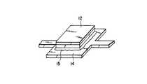
図1乃至図8はそれぞれ、この発明の第1の実施の形態に係るウェーハの分割方法及び半導体装置の製造方法について説明するためのもので、図1はダイシングラインに沿ってウェーハに溝を形成する工程、図2は溝の拡大断面図、図3(a),(b)はウェーハに表面保護テープを貼り付ける工程、図4はウェーハ裏面の研削及び研磨工程(分割工程)、図5はウェーハの研削及び研磨面が溝の底部に達してから、完成時のチップ厚になるまでの研削及び研磨量と、溝の底部における曲面を有する領域の深さとの比を変化させたときに、ウェーハの研削及び研磨面に発生するチッピングの平均径を測定した結果を示す図、図6は分離したチップをピックアップする工程、図7はダイボンディング工程及び図8は外囲器に封止する工程をそれぞれ示している。
【0043】
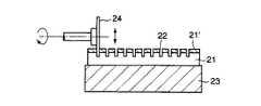
先ず、図1に示す如く、各種の半導体素子が形成されたウェーハ21をパターン形成面(ウェーハ21の主表面)21’側を上にして、ダイシング装置のチャックテーブル23にバキュームその他の方法で吸着して固定する。そして、先端部に曲面を有するダイシング用ブレード24を任意の回転数で回転させ、切削水を掛けながら所定の深さまでダイシングラインに沿って溝22を切り込む。この溝22の深さは、完成時のチップの厚さ(仕上げチップ厚)よりも少なくとも5μm、好ましくは5μm乃至60μm深くする。
【0044】
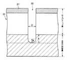
これによって、図2に示すように、幅(ダイシング用ブレード24の幅に対応する)がDで、底部に曲面を有する溝22が形成される。この溝22の曲面を有する領域の深さ(ダイシング用ブレード24における先端部の曲面を有する領域の突出量に対応する)はBである。
【0045】
なお、上記溝22は、上記ダイシング用ブレード24を用いて機械的に形成するだけでなく、エッチング等の化学的な方法で形成しても構わない。例えば、異方性エッチングと等方性エッチングを組み合わせることにより、図2に示したような断面形状の溝22を形成できる。すなわち、ウェーハ21の主表面21’上にフォトレジストを塗布し、PEP法等によりチップ分割ライン(ダイシングラインに対応する)上を露出させた後、KOH溶液に浸漬させることによりウェーハ21を深さ方向(ウェーハ21の主表面と直交する方向)に選択的にエッチングする。あるいは、KOH溶液を用いたウェットエッチングに代えて、RIE(Reactive Ion Etching)等のドライエッチング技術の適用も考えられる。例えば、真空度60mtorrでエッチングガスとしてSF6ガスやSF6/CF系混合ガスによりシリコンのみを選択的にエッチングすることが可能である。特に、SF6/CF系混合ガスでは良好な異方性エッチングが可能であり、ウェーハ21の主表面21’に対してほぼ垂直な溝加工が可能になる。その後、溝の底部を等方性エッチングすることにより、図2に示したように底部に曲面を持った溝22を形成する。
【0046】
上記エッチングを用いた溝22の形成方法は、ダイヤモンドブレード等のダイシング用ブレード24を用いる場合に比して、溝22の側壁(切断面)が機械的な応力の影響を受けないので、切断面に発生する結晶欠陥を低減できる。よって、必ずしも溝22の底部に曲面を形成しなくても良い。
【0047】
もちろん、上述した機械的あるいは化学的な形成方法だけでなく、レーザースクライバー等のような光学的な方法を用いて溝22を形成することもできる。この図1に示した工程で重要なのは、どのような方法で溝22を形成するかではなく、溝22の深さを、完成時のチップの厚さよりも少なくとも5μm、好ましくは5μm乃至60μm深く(但し、ウェーハ21が個々のチップに分離されないように)することである。
【0048】
その後、上記のようにして溝22を形成したウェーハ21の洗浄と乾燥処理を行う。
【0049】
次に、図3(a)に示すようなフラットリング25をパターン形成面の表面保護テープ(粘着性のシート)26に貼り付けて、このテープ26の弛みや皺を除去した状態で、図3(b)に示すように前工程で溝22を形成したウェーハ21のパターン形成面21’をテープ26の接着剤側に貼り付けて固定する。
【0050】
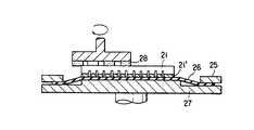
その後、図4に示すように、上記フラットリング25と表面保護テープ26とで保持されたウェーハ21を、研削装置のチャックテーブル27にバキューム等の方法で吸着固定する。そして、チャックテーブル27と研削用砥石28を回転させ、砥石28を降下させながらウェーハ21の裏面を削る。一般にこの研削方法はインフィード研削と呼ばれるものであるが、別の方法としてスルーフィード研削またはクリープフィード研削を用いても良い。上記ウェーハ21の裏面を、溝22に達するまで削ると、ウェーハ21は個々のチップ29に分割される。この発明では、ウェーハ21が個々のチップ29に分割された後も研削及び研磨を続け、完成時のチップの厚さ(仕上げチップ厚)にする。この際、上記研削及び研磨面が溝22の底部に達してから、完成時のチップの厚さになるまでの研削及び研磨量A(図2参照)と、上記溝22の底部の曲面を有する領域の深さBとの比(A/B)を0.3以上にする。
【0051】
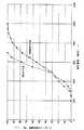
図5は、裏面研削時に研削面が溝22の底部に達してから仕上げチップ厚になるまでの研削量Aと、溝22の底部の曲面を有する領域の深さBとの比(A/B)を変えたときに、ウェーハ21の裏面に発生するチッピングの平均径を測定した結果を示している。図示するように、溝22の底部が平らな場合には14μm程度のチッピングが平均的に発生する。これに対し、A/Bが0.3以下では大きなチッピングが発生しているものの、0.3以上になると14μmより小さくなり、A/Bが1前後でのチッピングの平均径は5μmとなる。
【0052】
上記のように、ダイシングによって形成された切断面と研削及び研磨によって形成された研磨面とが交わる部分にチッピングが発生しても、この領域を研削及び研磨することによって除去できる。また、溝22の底部が曲面を有するので、ウェーハ21の裏面を研削及び研磨して行く際、溝22の底部のアーチ形状によってウェーハ21の大幅な強度向上が図れ、ウェーハ21が個々のチップに分離される直前におけるシリコン欠片の発生を抑制でき、チップ端面のダメージを抑えてチップ品質を向上できる。しかも、ウェーハ21の研削及び研磨面が溝の底部に達してから、完成時のチップ厚になるまでの研削及び研磨量と、溝の底部における曲面を有する領域の深さとの比を0.3以上にするので、研削及び研磨時に発生するチッピングの平均径をより小さくしてチップ品質を更に向上できる。また、溝の深さを完成時のチップの厚さよりも5μm乃至60μm深く形成しているので、未分離などの品質劣化を防止し、且つ研削量を最適化して生産性を落とすことなく研削異常を低減できる。これによって、本発明を用いれば、チップ29の完成時の厚さは、例えば30〜50μmまで薄厚化が可能となる。
【0053】
なお、上記ウェーハ21の裏面を、溝22に達するまで削って個々のチップ29に分割する際、1種類の砥粒径の研削砥石を用いても良いが、研削時間の短縮とチッピングの発生の防止との両方を考慮すると、次のように少なくとも2種類の砥粒径の研削砥石を用いて2段階、あるいはそれ以上で行うことが好ましい。すなわち、まず#360(主要な砥粒径が40〜60μm)程度の砥粒径の大きい研削砥石により研削及び研磨した後、#2000(主要な砥粒径が4〜6μm)程度の砥粒径の小さい研削砥石により研削及び研磨して個々のチップ29に分離すれば、ウェーハ21を個々のチップ29に分離するまでの時間短縮が図れ、且つ最終的に分離する際には砥粒径の小さい研削砥石を用いるのでチッピングの発生も低減できる。
【0054】
次に、図6に示すように、ウェーハ21の切断分離を終えて分割された個々のチップ29が接着固定されているフラットリング25をダイボンディング装置に設置し、このダイボンディング装置のピックアップニードル30を用いて表面保護テープ26越しにパターン形成面22に下方に圧力を加える。これによって、ピックアップニードル30は、テープ26を貫通することなくチップ29のパターン形成面を押圧し、チップ29がテープ26から剥離される。上記ピックアップニードル30は、先端曲率半径が0.35mm以上であれば18Nの力が掛かっても(15mm×15mmチップの場合)、チップ29中に形成されたアルミ配線等にダメージが発生しないことを本発明者等は実験により確認している。よって、チップ29の主表面側から表面保護テープ26を介してピックアップニードル30(金属製のピン)で押し剥がしても、先端曲率半径を最適化することによりピックアップニードル30がテープ26を破ることはなく、特に問題は発生しない。なお、本実施の形態では、チップ29をテープ26から剥離する際に、チップ29を押し下げるようにしたが、押し上げて剥離するようにしても良く、一般には後者の方法が多用されている。
【0055】
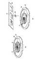
テープ26から剥離されたチップ29は、ダイボンディング装置のコレットと呼ばれるツールで吸着保持し、図7に示すようにリードフレームのアイランド31にマウントする。この際、リードフレームのアイランド31に予め接着固定用の導電性ペースト32を塗布しておき、その上にチップ29をダイボンディングする。金−シリコンの共晶を利用してマウントしたり、ウェーハの裏面に金属の薄膜を蒸着し、半田を用いてマウントすることもできる。
【0056】
その後、ワイヤボンディングを行ってチップ29の各パッドとリードフレーム34のインナーリード部とをボンディングワイヤ35で電気的に接続する。そして、チップ29、アイランド31及びリードフレーム34のインナーリード部を樹脂(またはセラミック)パッケージ33に封止し、リードフォーミングを行って図8に示すような半導体装置を完成する。
【0057】
図9(a),(b)はそれぞれ、ウェーハを個々のチップに分離した時の研削面の拡大図である。図9(a)は、従来の分割方法及び製造方法を用いた場合を示し、フルカットによってダイシングした時の研削面側の拡大図である。図示する如く、ダイシング部に多数のチッピングが発生している。図9(b)は、この発明の分割方法及び製造方法を用いた場合を示すもので、図9(a)に比べてシャープな切断面であり、チッピングは大幅に減少している。
【0058】
溝22の深さに関しては、裏面研削装置における研削部の精度、及び保護テープ部材の厚さの精度について検証したところ、下表1に示すように、最終的なチップ厚と一致(0)か5μm以下の範囲では、最悪の場合、未分離が発生してしまい、次のピックアップ工程においてクラックを発生させながらチップをピックアップすることになり、チップ裏面に著しいダメージを与える。
【0059】
これに対し、60μm以上の研削を行おうとすると、研削時間が長くなって生産性が低下する。特に、分割時間の短縮とチップの品質向上のために、粗研削と仕上げ研削を行う場合には、仕上げ研削の加工速度は粗研削の1/5〜1/10程度にする必要があり、且つ仕上げ研削砥石の特性上、研削量を大きく取ると研削面異常(砥石材料がウェーハ研削面に付着)が発生することからも溝22の深さをあまり深くできない。しかも、研削量を多くする場合には、2軸分離が前提となるが、2軸による低速での研削量が増えるために生産能力が大幅に低下するのみならず、2軸研削量が増えることで研削時の砥石への負担が増えて研削異常が発生し易くなる。従って、溝22の深さを60μm以上に深くするのは好ましくない。下表1に示すように、80μmでは研削異常が発生している。
【0060】
【表1】
これらのことから、好ましい溝の深さは「仕上げチップ厚+5μm」乃至「仕上げチップ厚+60μm」である。
【0062】
なお、上述した第1の実施の形態では、図1に示した工程においてウェーハ21に溝22を形成した後、図3(a),(b)に示したようにパターン形成面の表面保護テープ26にフラットリング25を貼り付け、このフラットリング25と表面保護テープ26とで保持されたウェーハ21を、研削装置のチャックテーブル27に吸着固定してウェーハ21の裏面を削った。しかしながら、フラットリング25はウェーハ21の裏面を削る工程では必ずしも必要ではなく、図10及び図11に示すようにフラットリングを用いなくても良い。すなわち、図1に示したような工程を経てウェーハ21に溝22を形成した後、ローラー51を図示矢印方向に移動させながらウェーハ21のパターン形成面(主表面)21’上に表面保護テープ(粘着性のシート)52を貼り付ける。その後、図11に示すように、表面保護テープ52で主表面が保護されたウェーハ21を、研削装置のチャックテーブル27にバキューム等の方法で吸着固定する。この際、フラットリングを使用していないので、ウェーハ21全体をフラットな状態で吸着する必要がある。引き続き、チャックテーブル27と研削用砥石28を回転させ、砥石28を降下させながらウェーハ21の裏面を削る。上記ウェーハ21の裏面を、溝22に達するまで削ると、ウェーハ21は個々のチップに分割される。ウェーハ21が個々のチップ29に分割された後も研削及び研磨を続け、少なくとも5μm以上、好ましくは5μm乃至60μm研削及び研磨する。次に、図12(a)に示すように、フラットリング25の粘着性のシート26上に前の工程で個々のチップ29に分割され表面保護テープ52で保持されているウェーハ21の裏面を貼り付ける。その後、図12(b)に示すように、表面保護テープ52を剥がす。以降の工程は、図6乃至図8に示した工程と同様である。
【0063】
なお、図6に示した工程でピックアップした個々のチップ29をダイボンディング、ワイヤボンディング及びパッケージへの封止工程等を経て半導体装置を完成するのではなく、トレイに詰めても良い。
【0064】
[第2の実施の形態]
図13は、この発明の第2の実施の形態に係る半導体装置の製造方法について説明するためのもので、LOC(Lead On Chip)パッケージに適用したものである。LOCパッケージの場合には、図6に示したピックアップ工程の後、次のような工程で封止する。まず、チップ29上に接着テープ36を介在させてリード37の一端を接着する。その後、ワイヤボンディングを行ってチップ29の各パッドとリード37とをボンディングワイヤ35で接続する。そして、樹脂パッケージ33またはセラミックパッケージに封止することにより、図13に示したような半導体装置が完成する。
【0065】
本実施の形態によれば、リード37の接着やワイヤボンディング時の荷重により、シリコン屑がチップ29表面の保護膜を破り、アルミ配線の段線やショート等の不良を起こす危険を抑制できる。
【0066】
上記のようなウェーハの分割方法及び半導体装置の製造方法によれば、下記(1)〜(6)に示すような効果が得られる。
【0067】
(1)ウェーハの薄厚化時のウェーハ破損による不良率の低減化が図れる。
【0068】
下表2は、6インチ型のウェーハを個々のチップに分割した場合のチップ厚(溝の深さと実質的に等しいか、あるいは少し薄い)と破損率(ppm:parts par million)との関係を示している。
【0069】
【表2】
表2に示す如く、従来はチップ厚が薄くなると破損率が高くなったが、この発明では最終的なチップ厚が薄くなるほど破損率が低くなる。これは、チップ厚を薄くする場合には溝を浅くすることができるので、溝の下に残存するウェーハ厚が厚くなることに依るものである。6インチ型のウェーハの場合には、ウェーハの厚さは通常600〜650μmである。従来の分割方法及び製造方法では、例えば50μmの厚さのチップを形成しようとすると、ウェーハを予め50μmの厚さに研削及び研磨し、図22乃至図24に示した処理を行う。これに対し、この発明の方法では、50μmの溝を形成した後(溝の下には550〜600μmのウェーハが残存されている)、研削及び研磨して個々のチップに分割するので破損率が低くなる。
【0071】
(2)搬送時のトラブルがウェーハの口径に左右されない。研削と同時にチップに分割するため、チップ厚が薄くなっても、あるいは同じ口径でも切削歪みによるウェーハの反りの影響を受けることなく装置内搬送が可能である。また、チップ厚が薄くなると溝の下に残存されるウェーハが厚くなるので、この点からも搬送時のウェーハ破損等を低減できる。これにより下表3のような効果が得られる。但し、ウェーハが8インチ型で、チップの厚さを50μmに仕上げる場合のものである。
【0072】
【表3】
この表3のデータから明らかなように、この発明はウェーハの大口径化に有効であり、今後展開されるウェーハの12インチ型化、または16インチ型化への対応が容易になる。
【0074】
(3)表面保護テープを一枚しか使用しないため、従来の方法に比して材料費と加工費を60%程度削減でき、製造コストの低減が図れる。
【0075】
(4)フルカット方式の場合、シートまで切り込むため、ブレードの切れ味の低下及びダイシング中のチップの飛散が生ずるため、一般的に80〜120mm/secであるが、この発明の方法では200mm/secまで可能である。これによって、ダイシングスピードの向上が図れ、10%程度の加工費の低減が図れる。
【0076】
(5)ウェーハを分割するために、ダイシングシートまで切り込む必要がなく、且つ裏面研削用の砥石で研削して分割するため、裏面チッピングの大きさが従来の15μm程度から4μm程度へと小さくなり、抗折強度が従来の方法では520MPaであったものが、600MPaまで向上する。
【0077】
なお、裏面研磨でチップ分割を行う際には、研削砥石のダイヤ砥粒径により裏面チッピング量が大きくなり、下表4のようにダイヤ砥粒径が小さい方が裏面チッピングが小さくなり、従って、チップの抗折強度がより向上する効果が得られる。よって、チップ分割時に使用する砥石のダイヤ砥粒径はできるだけ小さい方が好ましい。また、上述したように、砥粒径の大きい研削砥石と小さい研削砥石を組み合わせて用いることにより、チッピングを低減しつつ研削時間の短縮も図れる。
【0078】
【表4】
図14は、従来の方法とこの発明の方法による抗折強度分布を比較して示しており、各抗折強度(200MPa〜1000MPa)におけるチッピングの発生確率(%)を示している。この図14から明らかなように、この発明の分割方法では従来の分割方法に比して同一の抗折強度であればチッピングの発生確率が下がっており、高い抗折強度側にシフトしている。従来の方法による抗折強度の平均値は約520MPaであり、この発明の方法による抗折強度の平均値は約600MPaである。
【0080】
(6)ウェーハを分割するために、ダイシングシートまで切り込む必要がないため、ダイシングブレードの摩耗を低減でき、ダイシングブレードの寿命を向上できる。例えば、ダイシングシートまで切り込む方式を採用した場合には、通常10000〜20000ライン(6インチ型ウェーハの場合)の寿命であるが、この発明の方法では80000ライン以上にまで寿命を延ばすことが期待できる。
【0081】
[第3の実施の形態]
図15(a)〜(e)はそれぞれ、この発明の第3の実施の形態に係る半導体装置の製造方法について説明するためのもので、分割されたチップをリードフレームにマウントする工程を順次示している。まず、第1の実施の形態と同様に、図1乃至図4に示した工程に従ってウェーハ21を個々のチップ29に分割する。次に、分割された個々のチップ29が接着固定されているフラットリング25を研削装置のチャックテーブル27から取り外し、図15(a)に示すようにチップ29のピックアップを行う。この際、チップ29を下方から表面保護テープ26を介してピックアップニードルで突き上げて表面保護テープ26から剥離し、コレット38で裏面を吸着する。このコレット38はチップ反転機構を有しており、図15(b)に示す如く、下向きの吸着部が上向きになるように180°回転する。この状態で、チップ空中受け渡し機構を用いて、図15(c)に示すように別のコレット39に持ち替える。これによって、チップ29の表裏が反転して主表面(パターン形成面)が上向きとなる。その後、図15(d)に示すようにディスペンサ40を用いてリードフレーム34のアイランド31に導電性ペースト41を塗布し、図15(e)に示すように上記コレット39で保持しているチップ29を上記リードフレーム34のアイランド31上に移動させてダイボンディングする。
【0082】
[第4の実施の形態]
図16(a)〜(c)はそれぞれ、この発明の第4の実施の形態に係る半導体装置の製造方法について説明するためのもので、分割されたチップをリードフレームにマウントする工程を順次示している。まず、第1の実施の形態と同様に、図1乃至図4に示した工程に従ってウェーハ21を個々のチップ29に分割する。次に、分割された個々のチップ29が接着固定されているフラットリング25を研削装置のチャックテーブル27から取り外し、各チップ29を図16(a)に示すように表面保護テープ42にフラットリング43を張り付けたテープ表面に張り替える。これによって、チップ29の表裏が反転して主表面が上向きとなる。次に、図16(b)に示すようにディスペンサ40を用いてリードフレーム34のアイランド31に導電性ペースト41を塗布する。その後、図16(c)に示すようにピックアップニードルを用いた従来と同様なピックアップ、すなわち、表面保護テープ42越しに下方からパターン形成面に圧力を加えることによって、チップ29のパターン形成面を押圧し、チップ29を表面保護テープ42から剥離する。そして、コレット44でピックアップしたチップ29を上記導電性ペースト41を塗布したリードフレーム34のアイランド31上に移動させてダイボンディングする。
【0083】
[第5の実施の形態]
図17(a)〜(c)はそれぞれ、この発明の第5の実施の形態に係る半導体装置の製造方法について説明するためのもので、分割されたチップをリードフレームにマウントする工程を順次示している。まず、第1の実施の形態と同様に、図1乃至図4に示した工程に従ってウェーハ21を個々のチップ29に分割する。次に、分割された個々のチップ29が接着固定されているフラットリング25を研削装置のチャックテーブル27から取り外し、各チップ29をポーラスチャックテーブル45に移し替える。これによって、チップ29の表裏が反転して主表面が上向きとなる。次に、図17(b)に示すようにディスペンサ40を用いてリードフレーム34のアイランド31に導電性ペースト41を塗布する。その後、図17(c)に示すようにチップ29をポーラスチャックテーブル45からピックアップする。そして、上記ピックアップしたチップ29を上記リードフレーム34のアイランド31上に移動させてダイボンディングする。
【0084】
よって、上記第5の実施の形態では、突き上げピンを用いることなくチップ29のピックアップが可能となる。
【0085】
[第6の実施の形態]
図18(a)〜(e)はそれぞれ、この発明の第6の実施の形態に係る半導体装置の製造方法について説明するためのもので、分割されたチップをリードフレームにマウントする工程を順次示している。まず、第1の実施の形態と同様に、図1乃至図4に示した工程に従ってウェーハ21を個々のチップ29に分割する。次に、分割された個々のチップ29が接着固定されているフラットリング25を研削装置のチャックテーブル27から取り外し、図18(a)に示すようにコレット38を用いて各チップ29のピックアップを行う。ピックアップは、チップ29を表面保護テープ26を介して下方からピックアップニードルで突き上げて表面保護テープ26から剥離し、コレット38で吸着して行う。このコレット38はチップ反転機構を有しており、図18(b)に示す如く、下向きの吸着部が上向きとなるように180°回転する。この状態で、チップ空中受け渡し機構を用いて別のコレット39に持ち替える。次に、コレット39を移動させ、図18(c)に示すように各チップ29を表面保護テープ46にフラットリング47を張り付けたテープ表面に張り替える。これによって、各チップ29の表裏が反転して主表面(パターン形成面)が上向きとなる。次に、図18(d)に示すように、ディスペンサ40を用いてリードフレーム34のアイランド31に導電性ペースト41を塗布する。その後、図18(e)に示すようにピックアップニードルを用いた従来と同様なピックアップ、すなわち、表面保護テープ越しにチップ裏面に圧力を加えることによって、チップ裏面を押圧し、チップ29を表面保護テープから剥離する。そして、上記コレット39で保持しているチップ29を上記リードフレーム34のアイランド31上に移動させてダイボンディングする。
【0086】
上記マウント方法は、各チップ29をフラットリング47の表面保護テープ46に張り付けた状態で離れた位置にある製造装置、別の部屋や別の工場等に容易に輸送でき、種々の製造装置や製造方法に柔軟に対応できる。
【0087】
[第7の実施の形態]
図19(a)〜(e)はそれぞれ、この発明の第7の実施の形態に係る半導体装置の製造方法について説明するためのもので、分割されたチップをリードフレームにマウントする工程を順次示している。まず、第1の実施の形態と同様に、図1乃至図4に示した工程に従ってウェーハ21を個々のチップ29に分割する。次に、分割された個々のチップ29が接着固定されているフラットリング25を研削装置のチャックテーブル27から取り外し、図19(a)に示すようにチップ29のピックアップを行う。この際、チップ29を下方から表面保護テープ26を介してピックアップニードルで突き上げて表面保護テープ26から剥離し、コレット38で吸着する。このコレット38はチップ反転機構を有しており、図19(b)に示すように吸着部が下向きから上向きに180°回転する。この状態で、チップ空中受け渡し機構を用いて別のコレット39に持ち替える。次に、図19(c)に示すように、各チップ29をチップトレイ48に収容する。チップトレイ48にはチップ29の主表面(パターン形成面)が上向きに収容される。次に、図19(d)に示すようにディスペンサ40を用いてリードフレーム34のアイランド31に導電性ペースト41を塗布する。その後、図19(e)に示すようにコレット39でチップトレイ48から各チップ29を吸着し、上記コレット39で保持しているチップ29をリードフレーム34のアイランド31上に移動させてダイボンディングする。
【0088】
上記マウント方法では、上記第6の実施の形態と同様に、各チップ29をチップトレイ48に収容した状態で離れた位置にある製造装置、別の部屋や別の工場等に容易に輸送でき、種々の製造装置や製造方法に柔軟に対応できる。
【0089】
[第8の実施の形態]
図20(a)〜(d)はそれぞれ、この発明の第8の実施の形態に係る半導体装置の製造方法について説明するためのもので、分割されたチップをリードフレームにマウントする工程を順次示している。まず、第1の実施の形態と同様に、図1乃至図4に示した工程に従ってウェーハ21を個々のチップ29に分割する。次に、分割された個々のチップ29が接着固定されているフラットリング25を研削装置のチャックテーブル27から取り外し、図20(a)に示すようにチップ29のピックアップを行う。ピックアップは、チップ29を下方から表面保護テープ26を介してピックアップニードルで突き上げて表面保護テープ26から剥離し、コレット38で吸着して行う。この状態で、図20(b)に示すようにチップ29を加工ステージ49上に搬送して載置する。次に、図20(c)に示すように、ディスペンサ40を用いてリードフレーム34のアイランド31に導電性ペースト41を塗布する。この際、リードフレーム34のチップ搭載面を下方に向け、下方からディスペンサ40で導電性ペースト41をリードフレーム34の下面側に塗布する。そして、図20(d)に示すように上記加工ステージ49上に載置されているチップ29を上記リードフレーム34にダイボンディングする。
【0090】
このようなマウント方法では、チップ29の表裏を反転する必要がないので、コレット38にはチップ反転機構は不要であり、構造を簡単化できる。また、ピックアップしたチップを別の表面保護テープに張り替えたり、チップトレイに移し替えたりする必要もない。
【0091】
[第9の実施の形態]
図21(a),(b)はそれぞれ、この発明の第9の実施の形態に係る半導体装置の製造方法について説明するためのもので、分割されたチップをリードフレームにマウントする工程を順次示している。まず、第1の実施の形態と同様に、図1乃至図4に示した工程に従ってウェーハ21を個々のチップ29に分割する。次に、分割された個々のチップ29が接着固定されているフラットリング25を研削装置のチャックテーブル27から取り外し、図21(a)に示すように各チップ29の裏面に導電性ペースト41を塗布する。そして、図21(b)に示すように上記フラットリング25上にリードフレーム34を配置し、チップ29を下方から表面保護テープ26を介してピックアップニードルで突き上げて表面保護テープ26から剥離し、リードフレーム34のアイランド31にダイボンディングする。
【0092】
[変形例]
なお、この発明は上述した第1ないし第9の実施の形態に限定されるものではなく、要旨を逸脱しない範囲で種々変形して実施可能である。例えば、第1の実施の形態では、溝の形成時にウェーハ21をダイシング用チャックテーブル23に固着したが、従来の方法と同様にフラットリングを粘着性のシートに貼り付けた状態で、ウェーハをダイシング用チャックテーブルに固定するようにしても良い。あるいは、平板にウェーハを固定したり、平板に粘着性のシートを用いてウェーハを固着した状態で溝を形成しても良い。
【0093】
また、図4及び図11に示した研削及び研磨工程において、保持部材として表面保護テープ(粘着性のシート)26,52を用いたが、他の保持部材、例えばワックス、吸着パッド、熱圧着シート、粘着材を塗布した基板、及び半導体素子上に塗布したレジスト等、あるいはこれらを組み合わせた材料を用いることができる。
【0094】
更に、ウェーハ21のパターン形成面21’を粘着性のシート(表面保護テープ26)に貼り付けるようにしたが、ウェーハ21のパターン形成面21’と粘着性のシートとの間に極薄のフィルムを介在させても良い。極薄のフィルムを介在させるには、例えば、ウェーハのパターン形成面にシリテクト−IIと呼ばれる液体をスプレーで吹き付けて被膜を形成した後、粘着性のシートを貼り付ければ良い。平板上に両面あるいは片面の粘着テープを貼り付け、その上にウェーハを固着するようにしても良い。
【0095】
更に、チップを表面保護テープから剥離するためにピックアップニードルを用いたが、ピックアップニードルの代わりにチップ裏面をバキュームで吸着し、表面保護テープから剥離するようにしても良い。
【0096】
【発明の効果】
以上説明したように、この発明によれば、薄厚研削時や搬送時のウェーハの割れを抑制できるウェーハの分割方法及び半導体装置の製造方法が得られる。また、製造工程とコストの削減が図れるウェーハの分割方法及び半導体装置の製造方法が得られる。更に、ウェーハの裏面側のチッピングを小さくでき、チップの抗折応力の低下を抑制できるウェーハの分割方法及び半導体装置の製造方法が得られる。更に、ダイシングブレードの摩耗量の低減やダイシングブレードの寿命の向上等の効果も得られる。
【図面の簡単な説明】
【図1】この発明の第1の実施の形態に係る半導体装置の製造方法について説明するためのもので、ダイシングラインに沿ってウェーハに溝を形成する工程を示す側断面図。
【図2】図1に示した溝の拡大断面図。
【図3】この発明の第1の実施の形態に係る半導体装置の製造方法について説明するためのもので、(a)図はフラットリングの斜視図、(b)図はウェーハに表面保護テープを貼り付ける工程を示す断面図。
【図4】この発明の第1の実施の形態に係る半導体装置の製造方法について説明するためのもので、ウェーハ裏面の研削及び研磨工程(分割工程)を示す側断面図。
【図5】裏面研削時に研削面が溝の底部に達してから仕上げチップ厚になるまでの研削量と、溝の底部の曲面を有する領域の深さとの比を変えたときに、ウェーハの裏面に発生するチッピングの平均径を測定した結果を示す図。
【図6】この発明の第1の実施の形態に係る半導体装置の製造方法について説明するためのもので、分離したチップをピックアップする工程を示す側断面図。
【図7】この発明の第1の実施の形態に係る半導体装置の製造方法について説明するためのもので、ダイボンディング工程を示す斜視図。
【図8】この発明の第1の実施の形態に係る半導体装置の製造方法について説明するためのもので、外囲器に封止する工程を示す断面図。
【図9】従来とこの発明の方法でウェーハを個々のチップに分離した時の研削面の拡大図であり、(a)図は従来の方法による研削面、(b)図はこの発明の方法による研削面。
【図10】この発明の第1の実施の形態に係る半導体装置の製造方法の変形例について説明するためのもので、ウェーハに表面保護テープを貼り付ける工程を示す斜視図。
【図11】この発明の第1の実施の形態に係る半導体装置の製造方法の変形例について説明するためのもので、ウェーハ裏面の研削及び研磨工程(分割工程)を示す側断面図。
【図12】この発明の第1の実施の形態に係る半導体装置の製造方法の変形例について説明するためのもので、分離されたチップの転写工程(テープの張り替え工程)を示す斜視図であり、(a)図はフラットリングの粘着性のシート上にウェーハの裏面を貼り付ける工程、(b)図は表面保護テープを剥がす工程。
【図13】この発明の第2の実施の形態に係る半導体装置の製造方法について説明するためのもので、この発明をLOCパッケージに適用した時の半導体装置の断面図。
【図14】従来の方法とこの発明の方法による抗折強度分布を比較して示すダイヤグラム。
【図15】この発明の第3の実施の形態に係る半導体装置の製造方法について説明するためのもので、(a)図乃至(e)図はそれぞれ、分割されたチップをリードフレームにマウントする工程を順次示す斜視図。
【図16】この発明の第4の実施の形態に係る半導体装置の製造方法について説明するためのもので、(a)図乃至(c)図はそれぞれ、分割されたチップをリードフレームにマウントする工程を順次示す斜視図。
【図17】この発明の第5の実施の形態に係る半導体装置の製造方法について説明するためのもので、(a)図乃至(c)図はそれぞれ、分割されたチップをリードフレームにマウントする工程を順次示す斜視図。
【図18】この発明の第6の実施の形態に係る半導体装置の製造方法について説明するためのもので、(a)図乃至(e)図はそれぞれ、分割されたチップをリードフレームにマウントする工程を順次示す斜視図。
【図19】この発明の第7の実施の形態に係る半導体装置の製造方法について説明するためのもので、(a)図乃至(e)図はそれぞれ、分割されたチップをリードフレームにマウントする工程を順次示す斜視図。
【図20】この発明の第8の実施の形態に係る半導体装置の製造方法について説明するためのもので、(a)図乃至(d)図はそれぞれ、分割されたチップをリードフレームにマウントする工程を順次示す斜視図。
【図21】この発明の第9の実施の形態に係る半導体装置の製造方法について説明するためのもので、(a)図及び(b)図はそれぞれ、分割されたチップをリードフレームにマウントする工程を順次示す斜視図である。
【図22】従来の半導体装置の製造方法について説明するためのもので、ウェーハに表面保護テープを貼り付ける工程を示す側断面図。
【図23】従来の半導体装置の製造方法について説明するためのもので、ウェーハの裏面の研削及び研磨工程を示す側断面図。
【図24】従来の半導体装置の製造方法について説明するためのもので、表面保護テープを剥がす工程を示す側断面図。
【図25】従来の半導体装置の製造方法について説明するためのもので、(a)図はフラットリングの斜視図、(b)図はウェーハを固定用シートに固着した状態を示す断面図。
【図26】従来の半導体装置の製造方法について説明するためのもので、ウェーハのダイシング工程を示す側断面図。
【図27】従来の半導体装置の製造方法について説明するためのもので、分離したチップをピックアップする工程を示す側断面図。
【図28】従来の半導体装置の製造方法について説明するためのもので、ダイボンディング工程を示す斜視図。
【符号の説明】
21…ウェーハ
21’…パターン形成面
22…溝
24…ダイシング用ブレード
25,47…フラットリング
26,42,46…表面保護テープ
27…裏面研削用チャックテーブル
28…研削用砥石
29…チップ
30…ピックアップニードル
31…リードフレームのアイランド
32,41…導電性ペースト
33…パッケージ
34…リードフレーム
35…ボンディングワイヤ
36…接着テープ
37…リード
38,39,44…コレット
40…ディスペンサ
45…ポーラスチャックテーブル
A…研削量
B…底部の領域の深さ
D…溝の幅[0001]
BACKGROUND OF THE INVENTION
The present invention relates to a wafer dividing method and a semiconductor device manufacturing method, and more particularly, to a process of cutting and separating semiconductor elements formed on a wafer into individual chips and sealing them in an envelope. It is suitable for downsizing and thinning and increasing the diameter of a wafer.
[0002]
[Prior art]
In the manufacturing process of a semiconductor device, a pattern of various semiconductor elements is formed on a wafer (semiconductor substrate), and the semiconductor elements formed on the wafer are cut and separated into individual chips and sealed in an envelope. It can be roughly divided into processes. In recent years, an increase in wafer diameter has been promoted in order to reduce manufacturing costs, and in order to increase the mounting density, it has been desired to reduce the thickness and thickness of the envelope. Conventionally, in order to seal in a thin envelope, prior to cutting and separating the wafer into individual chips, the surface opposite to the pattern formation surface (main surface) of the wafer (back surface of the wafer) is used. It is removed and thinned by grinding with a grindstone, polishing with loose abrasive grains, etc., and then diced and cut and separated. At the time of grinding, the wafer is protected by sticking an adhesive sheet on the pattern forming surface of the wafer or applying a resist or the like. Thereafter, grooves are formed in a cutting separation (dicing) line region formed on the main surface of the wafer. In forming this groove, a diamond scriber, a diamond blade, a laser scriber, or the like is used. In the dicing process, the wafer is diced to half the thickness of the wafer or the half-cut method in which dicing is performed until the wafer remains about 30 μm. A half-cut method, a full-cut method in which an adhesive sheet is cut to about 20 to 30 μm and the entire wafer thickness is cut is used. The half-cut method requires a dividing operation. In the case of a single wafer, the wafer is sandwiched between a flexible film or the like, and is divided by applying an external force with a roller or the like. When pasted on a sheet, it is divided by applying an external force with a roller or the like through a tape. The divided chip pushes up the back surface of the sheet with a pickup needle provided in the die bonding apparatus, passes through the sheet, directly contacts the needle (needle) with the back surface of the chip, and further lifts the chip away from the sheet. The separated chip absorbs the chip surface with a tool called a collet, mounts it on the island of the lead frame, performs wire bonding, and electrically connects each pad of the chip and the inner lead part of the lead frame, The envelope is sealed. As a method of mounting the chip on the island, a method of applying a conductive paste to the island in advance, a method of mounting using a gold-silicon eutectic, and a metal thin film on the back surface of the wafer are deposited. There is a method of mounting using solder.
[0003]
FIG. 22 to FIG. 28 are for explaining detailed examples of the conventional wafer dividing method and semiconductor device manufacturing method as described above. FIG. 22 shows a process of attaching a surface protection tape to the wafer. 23 is a process for grinding and polishing the back surface of the wafer, FIG. 24 is a process for removing the surface protection tape, FIGS. 25A and 25B are processes for fixing the wafer to the fixing sheet, FIG. 26 is a process for dicing the wafer, and FIG. 27 shows a process of picking up separated chips, and FIG. 28 shows a die bonding process.
[0004]
First, as shown in FIG. 22, the back surface of the
[0005]
However, the above-described wafer dividing method and semiconductor device manufacturing method have the following problems (a) to (c).
[0006]
(A) The wafer is easily broken during thin grinding. Even if grinding is performed with a protective tape applied, the wafer is warped due to distortion during grinding, and therefore, the wafer is caught during transportation in the grinding apparatus and damaged. In addition, since the strength of the wafer decreases as the wafer becomes thinner or the diameter of the wafer increases, the method of carrying out various processes by transporting the wafer alone after thinning the wafer as in the present situation increases the probability of breakage. . For example, if the wafer is 400 μm thick, 1.6 kgf / mm2 Although it can withstand to the extent of 0.4 kgf / mm when the thickness is 200 μm2 And drop to 1/4.
[0007]
(B) Since two sheets are used to protect the pattern formation surface and hold the wafer during dicing, these need to be attached, peeled off, attached, and the process is increased, resulting in higher material costs and increased manufacturing processes. To do.
[0008]
(C) When dicing is performed, chipping on the back side of the wafer increases, leading to a reduction in the bending strength of the chip. Moreover, in the past, various characteristics monitoring transistors, resistors, capacitors, etc. (these are called TEG: Test Element Group) have been arranged in the chip. It came to arrange. As is well known, these elements are made of an oxide film, aluminum, or the like, and are materials that easily cause clogging of the grindstone and impair sharpness when dicing using a diamond blade. For this reason, when TEG is arrange | positioned on a dicing line, the chipping on the back surface side of a wafer becomes still larger. In general, since a material used as a semiconductor substrate is a brittle material such as silicon or GaAs, the presence of chipping or cracks tends to cause a decrease in bending strength.
[0009]
[Problems to be solved by the invention]
As described above, the conventional method for dividing a wafer and the method for manufacturing a semiconductor device have a problem that the wafer is easily broken during thin grinding or conveyance. Further, since two sheets are required for protecting the pattern formation surface and holding the wafer, there is a problem that the material cost increases and the manufacturing process increases. Further, when dicing is performed, chipping on the back surface side of the wafer becomes large, which causes a problem that the bending stress of the chip is lowered.
[0010]
The present invention has been made in view of the circumstances as described above, and an object thereof is to provide a wafer dividing method and a semiconductor device manufacturing method capable of suppressing cracking of the wafer during thin grinding or conveyance. It is in.
[0011]
Another object of the present invention is to provide a method for dividing a wafer and a method for manufacturing a semiconductor device, which can reduce the manufacturing process and cost.
[0012]
Still another object of the present invention is to provide a method for dividing a wafer and a method for manufacturing a semiconductor device that can reduce chipping on the back side of the wafer and suppress a reduction in chip bending stress.
[0013]
[Means for Solving the Problems]
The wafer dividing method according to the present invention uses a dicing blade having a curved surface at a tip portion along a dicing line of a wafer on which semiconductor elements are formed, and the thickness of the chip at the time of completion from the semiconductor element forming surface side. Each of the wafers by grinding and polishing the back surface of the wafer, and a step of forming a groove deeper than the depth and having a curved surface at the bottom, a step of attaching a holding member on the formation surface of the semiconductor element in the wafer, The wafer is divided into individual chips by grinding and polishing, and the grinding and polishing is continued even after the wafer is divided into individual chips, and the wafer is ground and polished to the thickness of the finished chip. The ratio of the amount of grinding and polishing until the chip thickness at the time of completion after reaching the bottom of the groove to the depth of the region having the curved surface at the bottom of the groove is 0. It is characterized in that at least.
[0015]
Further, in the wafer dividing method of the present invention, etching is performed along the chip dividing line of the wafer on which the semiconductor element is formed, so that the depth from the semiconductor element forming surface side is deeper than the chip thickness at the time of completion, and the bottom part. Forming a groove having a curved surface, a step of attaching a holding member on the surface of the semiconductor element on the wafer, grinding and polishing the back surface of the wafer, and separating the wafer into individual chips, And after the wafer has been divided into individual chips by grinding and polishing, the grinding and polishing is continued to the thickness of the chip at the completion, and the grinding and polishing surface of the wafer is at the bottom of the groove The ratio between the amount of grinding and polishing until reaching the chip thickness at the time of completion and the depth of the region having a curved surface at the bottom of the groove is 0.3 or more. It is set to.
[0016]
And it has the following features (A) to (E).
[0017]
(A) The depth of the groove is at least 5 μm deeper than the thickness of the completed chip.
[0018]
(B) The depth of the groove is 5 to 60 μm deeper than the thickness of the completed chip.
[0019]
(C) The holding member is at least one material selected from a tape with an adhesive, a wax, a suction pad, a thermocompression sheet, a substrate coated with an adhesive, and a resist coated on the semiconductor element. It is.
[0020]
(D) The step of grinding and polishing the back surface of the wafer to obtain a chip thickness at the time of completion comprises grinding the back surface of the wafer thicker than the chip at the time of completion with a grinding wheel having a first abrasive grain size. And a first step of polishing, and a back surface of the wafer ground and polished in the first step using a cutting grindstone having a second abrasive grain size smaller than the first abrasive grain size at the time of completion. And a second step of grinding and polishing to the thickness of the chip.
[0021]
(E) The main first abrasive particle size is 40 to 60 μm, and the main second abrasive particle size is 4 to 6 μm.
[0022]
According to the wafer dividing method as described above, a groove deeper than the chip thickness at the time of completion is formed from the element forming surface side of the wafer by using a dicing blade or by etching, and the back surface of the wafer is formed at the time of completion of the wafer. Since the wafer is separated into individual chips by grinding and polishing to the thickness of the chip, chipping during dicing can be suppressed. In addition, if a curved surface is formed at the bottom of the groove, when the back surface of the wafer is ground and polished, the arch shape at the bottom of the groove can greatly improve the strength of the wafer and immediately before the wafer is separated into individual chips. The generation of silicon fragments can be suppressed, and the chip quality can be improved by suppressing damage to the chip end face. Moreover, the ratio of the grinding and polishing amount from the time when the wafer grinding and polishing surface reaches the bottom of the groove to the chip thickness at the time of completion and the depth of the region having a curved surface at the bottom of the groove is 0.3 or more. By doing so, the average diameter of chipping generated during grinding and polishing can be further reduced to further improve the chip quality.
[0023]
Further, if the groove depth is at least 5 μm deeper than the finished chip thickness, preferably 5 μm to 60 μm deeper, quality degradation such as unseparation can be prevented, and the grinding amount can be optimized to reduce productivity. Grinding abnormality can be reduced without any problems. In addition, when the back surface of the wafer is ground and polished to be separated into individual chips, chipping may occur at the intersection of the cut surface formed by dicing or etching and the polished surface formed by grinding and polishing. This region can be removed by grinding and polishing.
[0024]
As the holding member, materials such as a tape with an adhesive material, a wax, an adsorption pad, a thermocompression bonding sheet, a substrate coated with an adhesive material, and a resist coated on a semiconductor element can be used.
[0025]
In the process of separating the wafer into individual chips, grinding and polishing with a grinding wheel with a large abrasive grain size and then grinding and polishing with a grinding wheel with a small abrasive grain size can reduce time and generate chipping. Can also be reduced.
[0026]
The method of manufacturing a semiconductor device according to the present invention includes a step of forming a semiconductor element on a main surface of a wafer, and a dicing blade having a curved surface at a tip portion along a dicing line of the wafer. Forming a groove deeper than the finished chip thickness from the side and having a curved surface at the bottom; attaching an adhesive sheet on the main surface of the wafer; and grinding and polishing the back surface of the wafer Then, the wafer is separated into individual chips, and after the wafer is divided into individual chips by grinding and polishing, the grinding and polishing are continued to obtain the thickness of the chip at the completion, and each of the separated And a step of peeling the chip from the adhesive sheet and sealing it in an envelope. After the grinding and polishing surface of the wafer reaches the bottom of the groove, the chip at the time of completion is provided. And grinding and polishing amount of up to a thickness, the ratio between the depth of the region having a curved surface at the bottom of the groove is characterized in that at least 0.3.
[0028]
Furthermore, the method for manufacturing a semiconductor device according to the present invention includes a step of forming a semiconductor element on a main surface of a wafer and etching along a chip dividing line of the wafer, thereby completing a chip at the time of completion from the main surface side of the wafer. Each of the wafers by grinding and polishing the back surface of the wafer, forming a groove deeper than the thickness of the groove and having a curved surface at the bottom, attaching an adhesive sheet on the main surface of the wafer, After the wafer is divided into individual chips by grinding and polishing, grinding and polishing are continued to obtain the thickness of the completed chip, and the separated chips are bonded to the adhesive. A process of peeling from the sheet and sealing in an envelope, and grinding from the wafer grinding and polishing surface to the bottom of the groove until the chip thickness is completed And fine polishing amount, the ratio between the depth of the region having a curved surface at the bottom of the groove is characterized in that at least 0.3.
[0029]
And it has the following features (F) to (K).
[0030]
(F) The depth of the groove is at least 5 μm deeper than the thickness of the completed chip.
[0031]
(G) The depth of the groove is 5 to 60 μm deeper than the thickness of the completed chip.
[0032]
(H) The step of separating the separated chips from the adhesive sheet and sealing them in an envelope includes the step of mounting the chip separated from the adhesive sheet on an island of a lead frame, and the lead Wire bonding the inner lead portion of the frame and each pad of the chip, and sealing the chip, the island, and the inner lead portion in an envelope.
[0033]
(I) The step of separating the separated chips from the adhesive sheet and sealing them in an envelope includes the step of adhering one end of a lead onto the main surface of the chip separated from the adhesive sheet. And a step of wire bonding the lead and each pad of the chip, and a step of sealing one end of the chip and the lead in an envelope.
[0034]
(J) The step of grinding and polishing the back surface of the wafer to obtain a chip thickness at the time of completion comprises grinding the back surface of the wafer to be thicker than the chip at the time of completion with a grinding wheel having a first abrasive grain size. And a first step of polishing, and a back surface of the wafer ground and polished in the first step using a cutting grindstone having a second abrasive grain size smaller than the first abrasive grain size at the time of completion. And a second step of grinding and polishing to the thickness of the chip.
[0035]
(K) The main first abrasive particle size is 40 to 60 μm, and the main second abrasive particle size is 4 to 6 μm.
[0036]
According to the semiconductor device manufacturing method as described above, the steps of cutting and separating the semiconductor elements formed on the wafer into individual chips and sealing them in the envelope are dicing (half cut), the back surface of the wafer The order is grinding and polishing, and die bonding. That is, the wafer is separated into individual chips by grinding and polishing. Therefore, since there is no conveyance or processing step in a state where the back surface of the wafer is thinned by grinding and polishing, damage to the wafer can be prevented.
[0037]
Since only one sheet is required, material costs and manufacturing processes can be reduced, and costs can be reduced. Since it is not necessary to divide the wafer by applying an external force, chipping can be suppressed.
[0038]
Since the back surface side of the wafer is removed by cutting and polishing and separated into individual chips, chipping generated on the back surface side of the wafer can be suppressed, and a decrease in bending stress can be suppressed. In addition, if a curved surface is formed at the bottom of the groove, when the back surface of the wafer is ground and polished, the arch shape at the bottom of the groove can greatly improve the strength of the wafer and immediately before the wafer is separated into individual chips. The generation of silicon fragments can be suppressed, and the chip quality can be improved by suppressing damage to the chip end face. Moreover, the ratio of the grinding and polishing amount from the time when the wafer grinding and polishing surface reaches the bottom of the groove to the chip thickness at the time of completion and the depth of the region having a curved surface at the bottom of the groove is 0.3 or more. Therefore, the chip quality can be further improved by reducing the average diameter of chipping generated during grinding and polishing.
[0039]
Furthermore, if the groove depth is at least 5 μm deeper than the chip thickness at the time of completion, preferably 5 μm to 60 μm deeper, quality degradation such as unseparation is prevented, and the amount of grinding is optimized to reduce productivity. Grinding abnormality can be reduced without any problems. In addition, when the back surface of the wafer is ground and polished to be separated into individual chips, even if chipping occurs at a portion where a cut surface formed by dicing or etching and a polished surface formed by grinding and polishing intersect, This region can be removed by grinding and polishing.
[0040]
When sealed in an envelope, it may be sealed in a normal resin package or ceramic package, or may be sealed in a LOC (Lead On Chip) package.
[0041]
Further, in the process of separating the wafer into individual chips, first, grinding and polishing with a grinding wheel having a large abrasive grain size, followed by grinding and polishing with a grinding wheel having a small abrasive grain size can reduce time and chipping. Can also be reduced.
[0042]
DETAILED DESCRIPTION OF THE INVENTION
Embodiments of the present invention will be described below with reference to the drawings.
[First Embodiment]
1 to 8 are for explaining a wafer dividing method and a semiconductor device manufacturing method according to the first embodiment of the present invention, respectively, and FIG. 1 forms grooves in the wafer along dicing lines. 2 is an enlarged cross-sectional view of the groove, FIGS. 3A and 3B are steps of attaching a surface protection tape to the wafer, FIG. 4 is a grinding and polishing step (dividing step) of the wafer back surface, and FIG. When the grinding and polishing surface of the wafer reaches the bottom of the groove and the ratio of the grinding and polishing amount until the chip thickness at the time of completion and the depth of the region having a curved surface at the bottom of the groove is changed, The figure which shows the result of having measured the average diameter of the chipping which generate | occur | produces on the grinding and polishing surface of a wafer, FIG. 6 is the process of picking up the separated chip, FIG. 7 is the die bonding process, and FIG. 8 is the process of sealing in the envelope It It is shows.
[0043]
First, as shown in FIG. 1, a
[0044]
As a result, as shown in FIG. 2, a
[0045]
The
[0046]
The method of forming the
[0047]
Of course, the
[0048]
Thereafter, the
[0049]
Next, a
[0050]
Thereafter, as shown in FIG. 4, the
[0051]
FIG. 5 shows a ratio (A / B) between the grinding amount A from the time when the ground surface reaches the bottom of the
[0052]
As described above, even if chipping occurs at a portion where a cut surface formed by dicing and a polished surface formed by grinding and polishing intersect, this region can be removed by grinding and polishing. Further, since the bottom of the
[0053]
In addition, when the back surface of the
[0054]
Next, as shown in FIG. 6, the
[0055]
The
[0056]
Thereafter, wire bonding is performed to electrically connect each pad of the
[0057]
FIGS. 9A and 9B are enlarged views of the grinding surface when the wafer is separated into individual chips. Fig.9 (a) shows the case where the conventional division | segmentation method and manufacturing method are used, and is an enlarged view by the side of the grinding surface when dicing by a full cut. As shown in the figure, many chippings are generated in the dicing part. FIG. 9B shows a case where the dividing method and the manufacturing method of the present invention are used, and it has a sharp cut surface as compared with FIG. 9A, and chipping is greatly reduced.
[0058]
As for the depth of the
[0059]
On the other hand, if grinding of 60 μm or more is attempted, the grinding time becomes longer and the productivity is lowered. In particular, when rough grinding and finish grinding are performed in order to shorten the division time and improve chip quality, the processing speed of finish grinding needs to be about 1/5 to 1/10 that of rough grinding, and Due to the characteristics of the finish grinding wheel, if the grinding amount is large, the grinding surface abnormalities (the grinding stone material adheres to the wafer grinding surface) may occur, so that the depth of the
[0060]
[Table 1]
Therefore, the preferable depth of the groove is “finish chip thickness + 5 μm” to “finish chip thickness + 60 μm”.
[0062]
In the first embodiment described above, after forming the
[0063]
The
[0064]
[Second Embodiment]
FIG. 13 illustrates a method for manufacturing a semiconductor device according to the second embodiment of the present invention, which is applied to a LOC (Lead On Chip) package. In the case of the LOC package, after the pickup process shown in FIG. First, one end of the
[0065]
According to the present embodiment, it is possible to suppress the risk of silicon scraps breaking the protective film on the surface of the
[0066]
According to the above wafer dividing method and semiconductor device manufacturing method, the following effects (1) to (6) can be obtained.
[0067]
(1) It is possible to reduce the defect rate due to wafer breakage when the wafer is thinned.
[0068]
Table 2 below shows the relationship between chip thickness (substantially equal to or slightly thinner than the groove depth) and breakage rate (ppm) when a 6-inch wafer is divided into individual chips. Show.
[0069]
[Table 2]
As shown in Table 2, conventionally, the breakage rate increased as the chip thickness decreased, but in the present invention, the breakage rate decreased as the final chip thickness decreased. This is because when the chip thickness is reduced, the groove can be made shallower, so that the thickness of the wafer remaining under the groove is increased. In the case of a 6-inch type wafer, the thickness of the wafer is usually 600 to 650 μm. In the conventional dividing method and manufacturing method, for example, in order to form a chip having a thickness of 50 μm, the wafer is ground and polished to a thickness of 50 μm in advance, and the processes shown in FIGS. 22 to 24 are performed. On the other hand, in the method of the present invention, after forming a 50 μm groove (a 550 to 600 μm wafer remains under the groove), grinding and polishing are performed and divided into individual chips, so the damage rate is high. Lower.
[0071]
(2) Troubles during transfer are not affected by the diameter of the wafer. Since it is divided into chips simultaneously with grinding, even if the chip thickness is reduced, or even with the same diameter, it can be transferred within the apparatus without being affected by the warping of the wafer due to cutting distortion. Further, since the wafer remaining under the groove becomes thicker as the chip thickness becomes thinner, the wafer breakage during the transportation can be reduced also from this point. As a result, the effects shown in Table 3 below are obtained. However, this is a case where the wafer is an 8-inch type and the chip thickness is finished to 50 μm.
[0072]
[Table 3]
As apparent from the data in Table 3, the present invention is effective for increasing the diameter of the wafer, and it becomes easy to cope with the 12-inch type or 16-inch type of wafers to be developed in the future.
[0074]
(3) Since only one surface protection tape is used, the material cost and the processing cost can be reduced by about 60% as compared with the conventional method, and the manufacturing cost can be reduced.
[0075]
(4) In the case of the full cut method, since cutting to the sheet results in a reduction in blade sharpness and chip scattering during dicing, it is generally 80 to 120 mm / sec. However, in the method of the present invention, 200 mm / sec. Is possible. As a result, the dicing speed can be improved, and the processing cost can be reduced by about 10%.
[0076]
(5) In order to divide the wafer, it is not necessary to cut up to a dicing sheet, and since it is divided by grinding with a grinding wheel for back surface grinding, the size of the back surface chipping is reduced from about 15 μm to about 4 μm, The bending strength of the conventional method, which was 520 MPa, is improved to 600 MPa.
[0077]
In addition, when performing chip division by back surface polishing, the back surface chipping amount increases due to the diamond abrasive particle size of the grinding wheel, and the back surface chipping decreases when the diamond abrasive particle size is small as shown in Table 4 below. An effect of further improving the bending strength of the chip can be obtained. Therefore, it is preferable that the diamond abrasive grain size of the grindstone used at the time of chip division is as small as possible. Further, as described above, by using a combination of a grinding wheel having a large abrasive grain size and a small grinding wheel, the grinding time can be shortened while reducing chipping.
[0078]
[Table 4]
FIG. 14 shows a comparison of bending strength distributions according to the conventional method and the method of the present invention, and shows the occurrence probability (%) of chipping at each bending strength (200 MPa to 1000 MPa). As is apparent from FIG. 14, in the dividing method of the present invention, the probability of chipping is lowered when the bending strength is the same as that of the conventional dividing method, and it is shifted to a higher bending strength side. . The average value of the bending strength according to the conventional method is about 520 MPa, and the average value of the bending strength according to the method of the present invention is about 600 MPa.
[0080]
(6) Since it is not necessary to cut the dicing sheet to divide the wafer, wear of the dicing blade can be reduced and the life of the dicing blade can be improved. For example, when a method of cutting up to a dicing sheet is adopted, the life is normally 10,000 to 20000 lines (in the case of a 6-inch wafer), but the method of the present invention can be expected to extend the life to 80000 lines or more. .
[0081]
[Third Embodiment]
FIGS. 15A to 15E are diagrams for explaining a method of manufacturing a semiconductor device according to the third embodiment of the present invention, and sequentially show the steps of mounting the divided chips on the lead frame. ing. First, as in the first embodiment, the
[0082]
[Fourth Embodiment]
FIGS. 16A to 16C are respectively for explaining a method of manufacturing a semiconductor device according to the fourth embodiment of the present invention, and sequentially show the steps of mounting the divided chips on the lead frame. ing. First, as in the first embodiment, the
[0083]
[Fifth Embodiment]
FIGS. 17A to 17C are for explaining a method of manufacturing a semiconductor device according to the fifth embodiment of the present invention, and sequentially show the steps of mounting the divided chips on the lead frame. ing. First, as in the first embodiment, the
[0084]
Therefore, in the fifth embodiment, the
[0085]
[Sixth Embodiment]
18 (a) to 18 (e) are respectively for explaining a method of manufacturing a semiconductor device according to the sixth embodiment of the present invention, and sequentially show the steps of mounting the divided chips on the lead frame. ing. First, as in the first embodiment, the
[0086]
In the mounting method, each
[0087]
[Seventh Embodiment]
FIGS. 19A to 19E are for explaining a method of manufacturing a semiconductor device according to the seventh embodiment of the present invention, and sequentially show the steps of mounting the divided chips on the lead frame. ing. First, as in the first embodiment, the
[0088]
In the mounting method, as in the sixth embodiment, each
[0089]
[Eighth Embodiment]
FIGS. 20A to 20D are respectively for explaining a method of manufacturing a semiconductor device according to the eighth embodiment of the present invention, and sequentially show the steps of mounting the divided chips on the lead frame. ing. First, as in the first embodiment, the
[0090]
In such a mounting method, since it is not necessary to reverse the front and back of the
[0091]
[Ninth Embodiment]
FIGS. 21A and 21B are views for explaining a method of manufacturing a semiconductor device according to the ninth embodiment of the present invention, and sequentially show the steps of mounting the divided chips on the lead frame. ing. First, as in the first embodiment, the
[0092]
[Modification]
The present invention is not limited to the first to ninth embodiments described above, and various modifications can be made without departing from the spirit of the invention. For example, in the first embodiment, the
[0093]
Further, in the grinding and polishing steps shown in FIGS. 4 and 11, surface protection tapes (adhesive sheets) 26 and 52 are used as holding members, but other holding members such as wax, suction pads, and thermocompression bonding sheets are used. Further, a substrate coated with an adhesive material, a resist coated on a semiconductor element, or a combination of these can be used.
[0094]
Further, the
[0095]
Further, the pick-up needle is used to peel the chip from the surface protective tape. However, instead of the pick-up needle, the back surface of the chip may be adsorbed by vacuum and peeled from the surface protective tape.
[0096]
【The invention's effect】
As described above, according to the present invention, a method for dividing a wafer and a method for manufacturing a semiconductor device that can suppress cracking of the wafer during thin grinding or conveyance can be obtained. Further, a wafer dividing method and a semiconductor device manufacturing method that can reduce the manufacturing process and cost can be obtained. Furthermore, chipping on the back surface side of the wafer can be reduced, and a wafer dividing method and a semiconductor device manufacturing method that can suppress a reduction in chip bending stress can be obtained. Furthermore, effects such as reduction of the amount of wear of the dicing blade and improvement of the life of the dicing blade can be obtained.
[Brief description of the drawings]
FIG. 1 is a side cross-sectional view for explaining a method of manufacturing a semiconductor device according to a first embodiment of the present invention and showing a step of forming a groove in a wafer along a dicing line.
FIG. 2 is an enlarged cross-sectional view of the groove shown in FIG.
3A and 3B are diagrams for explaining a method of manufacturing a semiconductor device according to the first embodiment of the present invention. FIG. 3A is a perspective view of a flat ring, and FIG. Sectional drawing which shows the process of affixing.
FIG. 4 is a side cross-sectional view for explaining a method for manufacturing a semiconductor device according to the first embodiment of the present invention, showing a grinding and polishing process (dividing process) on the back surface of the wafer;
FIG. 5 shows the back surface of the wafer when the ratio of the amount of grinding from when the grinding surface reaches the bottom of the groove to the finished chip thickness during back surface grinding and the depth of the region having the curved surface at the bottom of the groove is changed. The figure which shows the result of having measured the average diameter of the chipping which generate | occur | produces.
FIG. 6 is a side sectional view for explaining the method for manufacturing the semiconductor device according to the first embodiment of the present invention and showing a step of picking up separated chips;
FIG. 7 is a perspective view showing a die bonding step for explaining the method of manufacturing the semiconductor device according to the first embodiment of the invention.
FIG. 8 is a cross-sectional view showing a step of sealing the envelope for explaining the method of manufacturing the semiconductor device according to the first embodiment of the invention.
FIG. 9 is an enlarged view of a ground surface when a wafer is separated into individual chips by the conventional method and the method of the present invention, (a) is a ground surface by a conventional method, and (b) is a method of the present invention. By grinding surface.
FIG. 10 is a perspective view for illustrating a modification of the method for manufacturing the semiconductor device according to the first embodiment of the present invention and illustrating a step of attaching a surface protection tape to the wafer.
FIG. 11 is a sectional side view for explaining a modification of the semiconductor device manufacturing method according to the first embodiment of the present invention and showing a grinding and polishing process (dividing process) of the wafer back surface;
FIG. 12 is a perspective view for explaining a modified example of the semiconductor device manufacturing method according to the first embodiment of the present invention and showing a separated chip transfer process (tape replacement process); (A) A figure is the process of sticking the back surface of a wafer on the adhesive sheet of a flat ring, (b) A figure is the process of peeling off a surface protection tape.
FIG. 13 is a cross-sectional view of a semiconductor device when the present invention is applied to a LOC package for explaining a method of manufacturing a semiconductor device according to a second embodiment of the present invention.
FIG. 14 is a diagram showing a comparison of bending strength distributions according to the conventional method and the method of the present invention.
FIGS. 15A to 15E are views for explaining a method of manufacturing a semiconductor device according to a third embodiment of the present invention. FIGS. 15A to 15E each mount a divided chip on a lead frame. FIGS. The perspective view which shows a process in order.
FIGS. 16A to 16C are views for explaining a method of manufacturing a semiconductor device according to a fourth embodiment of the present invention. FIGS. 16A to 16C each mount a divided chip on a lead frame. The perspective view which shows a process in order.
FIGS. 17A to 17C are views for explaining a method of manufacturing a semiconductor device according to a fifth embodiment of the present invention. FIGS. 17A to 17C each mount a divided chip on a lead frame. The perspective view which shows a process in order.
FIGS. 18A to 18E are views for explaining a method of manufacturing a semiconductor device according to a sixth embodiment of the present invention. FIGS. 18A to 18E each mount a divided chip on a lead frame. FIGS. The perspective view which shows a process in order.
FIGS. 19A to 19E are views for explaining a method of manufacturing a semiconductor device according to a seventh embodiment of the present invention. FIGS. 19A to 19E each mount a divided chip on a lead frame. FIGS. The perspective view which shows a process in order.
FIGS. 20A to 20D are views for explaining a method of manufacturing a semiconductor device according to an eighth embodiment of the present invention, and FIGS. 20A to 20D each mount a divided chip on a lead frame; FIGS. The perspective view which shows a process in order.
FIGS. 21A and 21B are views for explaining a method of manufacturing a semiconductor device according to a ninth embodiment of the present invention. FIGS. 21A and 21B each mount a divided chip on a lead frame; FIGS. It is a perspective view which shows a process in order.
FIG. 22 is a side sectional view for explaining a conventional method of manufacturing a semiconductor device and showing a step of attaching a surface protection tape to a wafer.
FIG. 23 is a side sectional view for explaining a conventional method for manufacturing a semiconductor device, showing a grinding and polishing process of a back surface of a wafer.
FIG. 24 is a side sectional view for explaining a conventional method of manufacturing a semiconductor device and showing a step of peeling off the surface protection tape.
25A and 25B are views for explaining a conventional method of manufacturing a semiconductor device, in which FIG. 25A is a perspective view of a flat ring, and FIG.
FIG. 26 is a side sectional view showing a wafer dicing step for explaining a conventional method of manufacturing a semiconductor device;
FIG. 27 is a side cross-sectional view illustrating a process of picking up a separated chip for explaining a conventional method of manufacturing a semiconductor device.
FIG. 28 is a perspective view showing a die bonding step for explaining a conventional method of manufacturing a semiconductor device.
[Explanation of symbols]
21 ... Wafer
21 '... pattern formation surface
22 ... Groove
24 ... Blade for dicing
25, 47 ... Flat ring
26, 42, 46 ... surface protection tape
27 ... Chuck table for back grinding
28 ... Wheel for grinding
29 ... chip
30 ... Pickup needle
31 ... Lead frame island
32, 41 ... conductive paste
33 ... Package
34 ... Lead frame
35 ... Bonding wire
36 ... Adhesive tape
37 ... Lead
38, 39, 44 ... Collet
40 ... dispenser
45 ... Porous chuck table
A ... grinding amount
B: Depth of bottom area
D: Groove width
Claims (15)
Translated fromJapanese前記ウェーハにおける前記半導体素子の形成面上に保持部材を貼り付ける工程と、
前記ウェーハの裏面を研削及び研磨して、ウェーハを個々のチップに分離し、研削及び研磨によってウェーハが個々のチップに分割された後も研削及び研磨を続け、前記完成時のチップの厚さにする工程とを具備し、
前記ウェーハの研削及び研磨面が前記溝の底部に達してから、完成時のチップ厚になるまでの研削及び研磨量と、前記溝の底部における曲面を有する領域の深さとの比が0.3以上であることを特徴とするウェーハの分割方法。Using a dicing blade having a curved surface at the tip along the dicing line of the wafer on which the semiconductor element is formed, the curved surface is formed deeper than the chip thickness at the time of completion from the semiconductor element formation surface side. Forming a groove having,
A step of attaching a holding member on the formation surface of the semiconductor element in the wafer;
The back surface of the wafer is ground and polished to separate the wafer into individual chips. After the wafer is divided into individual chips by grinding and polishing, the grinding and polishing are continued to obtain the thickness of the finished chip. Comprising the steps of:
The ratio of the amount of grinding and polishing from the time when the grinding and polishing surface of the wafer reaches the bottom of the groove to the chip thickness at the time of completion and the depth of the region having a curved surface at the bottom of the groove is 0.3. A wafer dividing method as described above.
前記ウェーハにおける前記半導体素子の形成面上に保持部材を貼り付ける工程と、
前記ウェーハの裏面を研削及び研磨して、ウェーハを個々のチップに分離し、研削及び研磨によってウェーハが個々のチップに分割された後も研削及び研磨を続け、前記完成時のチップの厚さにする工程とを具備し、
前記ウェーハの研削及び研磨面が前記溝の底部に達してから、完成時のチップ厚になるまでの研削及び研磨量と、前記溝の底部における曲面を有する領域の深さとの比が0.3以上であることを特徴とするウェーハの分割方法。Etching along the chip dividing line of the wafer on which the semiconductor element is formed, forming a groove having a curved surface at the bottom and deeper than the completed chip thickness from the semiconductor element forming surface side;
A step of attaching a holding member on a formation surface of the semiconductor element in the wafer;
The back surface of the wafer is ground and polished to separate the wafer into individual chips, and after the wafer is divided into individual chips by grinding and polishing, grinding and polishing are continued to obtain the thickness of the finished chip. Comprising the steps of:
The ratio of the grinding and polishing amount from the time when the grinding and polishing surface of the wafer reaches the bottom of the groove to the chip thickness at the time of completion and the depth of the region having a curved surface at the bottom of the groove is 0.3. A wafer dividing method as described above.
前記ウェーハのダイシングラインに沿って、先端部に曲面を有するダイシング用ブレードを用いて、前記ウェーハの主表面側から完成時のチップの厚さよりも深く、且つ底部に曲面を有する溝を形成する工程と、
前記ウェーハの主表面上に粘着性のシートを貼り付ける工程と、
前記ウェーハの裏面を研削及び研磨して、ウェーハを個々のチップに分離し、研削及び研磨によってウェーハが個々のチップに分割された後も研削及び研磨を続け、前記完成時のチップの厚さにする工程と、
前記分離した各チップを前記粘着性のシートから剥離して外囲器に封止する工程とを具備し、
前記ウェーハの研削及び研磨面が前記溝の底部に達してから、完成時のチップ厚になるまでの研削及び研磨量と、前記溝の底部における曲面を有する領域の深さとの比が0.3以上であることを特徴とする半導体装置の製造方法。Forming a semiconductor element on the main surface of the wafer;
A step of forming a groove having a curved surface at the bottom and deeper than the completed chip thickness from the main surface side of the wafer by using a dicing blade having a curved surface at the tip along the dicing line of the wafer. When,
Adhering an adhesive sheet on the main surface of the wafer;
The back surface of the wafer is ground and polished to separate the wafer into individual chips, and after the wafer is divided into individual chips by grinding and polishing, grinding and polishing are continued to obtain the thickness of the finished chip. And a process of
Separating the separated chips from the adhesive sheet and sealing them in an envelope,
The ratio of the grinding and polishing amount from the time when the grinding and polishing surface of the wafer reaches the bottom of the groove to the chip thickness at the time of completion and the depth of the region having a curved surface at the bottom of the groove is 0.3. This is the method for manufacturing a semiconductor device.
前記ウェーハのチップ分割ラインに沿ってエッチングすることにより、前記ウェーハの主表面側から完成時のチップの厚さよりも深く、且つ底部に曲面を有する溝を形成する工程と、
前記ウェーハの主表面上に粘着性のシートを貼り付ける工程と、
前記ウェーハの裏面を研削及び研磨して、ウェーハを個々のチップに分離し、研削及び研磨によってウェーハが個々のチップに分割された後も研削及び研磨を続け、前記完成時のチップの厚さにする工程と、
前記分離した各チップを前記粘着性のシートから剥離して外囲器に封止する工程とを具備し、
前記ウェーハの研削及び研磨面が前記溝の底部に達してから、完成時のチップ厚になるまでの研削及び研磨量と、前記溝の底部における曲面を有する領域の深さとの比が0.3以上であることを特徴とする半導体装置の製造方法。Forming a semiconductor element on the main surface of the wafer;
Etching along the chip splitting line of the wafer to form a groove having a curved surface at the bottom and deeper than the thickness of the completed chip from the main surface side of the wafer;
Adhering an adhesive sheet on the main surface of the wafer;
The back surface of the wafer is ground and polished to separate the wafer into individual chips, and after the wafer is divided into individual chips by grinding and polishing, grinding and polishing are continued to obtain the thickness of the finished chip. And a process of
Separating the separated chips from the adhesive sheet and sealing them in an envelope,
The ratio of the grinding and polishing amount from the time when the grinding and polishing surface of the wafer reaches the bottom of the groove to the chip thickness at the time of completion and the depth of the region having a curved surface at the bottom of the groove is 0.3. This is the method for manufacturing a semiconductor device.
Priority Applications (1)
| Application Number | Priority Date | Filing Date | Title |
|---|---|---|---|
| JP2000013231AJP4040819B2 (en) | 1999-02-03 | 2000-01-21 | Wafer dividing method and semiconductor device manufacturing method |
Applications Claiming Priority (3)
| Application Number | Priority Date | Filing Date | Title |
|---|---|---|---|
| JP11-25644 | 1999-02-03 | ||
| JP2564499 | 1999-02-03 | ||
| JP2000013231AJP4040819B2 (en) | 1999-02-03 | 2000-01-21 | Wafer dividing method and semiconductor device manufacturing method |
Publications (2)
| Publication Number | Publication Date |
|---|---|
| JP2000294522A JP2000294522A (en) | 2000-10-20 |
| JP4040819B2true JP4040819B2 (en) | 2008-01-30 |
Family
ID=26363288
Family Applications (1)
| Application Number | Title | Priority Date | Filing Date |
|---|---|---|---|
| JP2000013231AExpired - LifetimeJP4040819B2 (en) | 1999-02-03 | 2000-01-21 | Wafer dividing method and semiconductor device manufacturing method |
Country Status (1)
| Country | Link |
|---|---|
| JP (1) | JP4040819B2 (en) |
Families Citing this family (20)
| Publication number | Priority date | Publication date | Assignee | Title |
|---|---|---|---|---|
| JP4659300B2 (en) | 2000-09-13 | 2011-03-30 | 浜松ホトニクス株式会社 | Laser processing method and semiconductor chip manufacturing method |
| JP2003007653A (en)* | 2001-06-26 | 2003-01-10 | Disco Abrasive Syst Ltd | Semiconductor wafer division system and division method |
| JP4669162B2 (en)* | 2001-06-28 | 2011-04-13 | 株式会社ディスコ | Semiconductor wafer dividing system and dividing method |
| JP4330821B2 (en) | 2001-07-04 | 2009-09-16 | 株式会社東芝 | Manufacturing method of semiconductor device |
| US8048774B2 (en)* | 2001-10-01 | 2011-11-01 | Electro Scientific Industries, Inc. | Methods and systems for laser machining a substrate |
| WO2003076119A1 (en) | 2002-03-12 | 2003-09-18 | Hamamatsu Photonics K.K. | Method of cutting processed object |
| TWI326626B (en) | 2002-03-12 | 2010-07-01 | Hamamatsu Photonics Kk | Laser processing method |
| EP2400539B1 (en)* | 2002-03-12 | 2017-07-26 | Hamamatsu Photonics K.K. | Substrate dividing method |
| JP2004031844A (en)* | 2002-06-28 | 2004-01-29 | Sony Corp | Method of manufacturing semiconductor chip and manufacturing apparatus for semiconductor chip |
| US7233413B2 (en) | 2002-11-22 | 2007-06-19 | E. I. Du Pont De Nemours And Company | Gamut description and visualization |
| TWI520269B (en) | 2002-12-03 | 2016-02-01 | Hamamatsu Photonics Kk | Cutting method of semiconductor substrate |
| DE60315515T2 (en) | 2003-03-12 | 2007-12-13 | Hamamatsu Photonics K.K., Hamamatsu | LASER PROCESSING PROCEDURES |
| TWI239629B (en) | 2003-03-17 | 2005-09-11 | Seiko Epson Corp | Method of manufacturing semiconductor device, semiconductor device, circuit substrate and electronic apparatus |
| JP4234630B2 (en) | 2003-05-29 | 2009-03-04 | 古河電気工業株式会社 | Method of manufacturing thin film circuit board having penetrating structure and protective adhesive tape |
| JP4652986B2 (en)* | 2006-02-08 | 2011-03-16 | 株式会社ディスコ | Liquid resin coating apparatus and laser processing apparatus |
| JP2008153349A (en)* | 2006-12-15 | 2008-07-03 | Disco Abrasive Syst Ltd | Wafer dividing method |
| JP2008034875A (en)* | 2007-10-09 | 2008-02-14 | Toshiba Corp | Semiconductor device and manufacturing method thereof |
| JP2013172115A (en)* | 2012-02-23 | 2013-09-02 | Zhihao Chen | Wafer manufacturing method for ecological processing |
| CN112614878A (en)* | 2021-01-19 | 2021-04-06 | 浙江宏禧科技有限公司 | Manufacturing method of single-curved-surface silicon-based micro display |
| CN113496929B (en)* | 2021-07-07 | 2022-06-10 | 哈尔滨宇龙自动化有限公司 | Micro-connection separation device for PLC type optical chip sealing and measuring processing and use method |
- 2000
- 2000-01-21JPJP2000013231Apatent/JP4040819B2/ennot_activeExpired - Lifetime
Also Published As
| Publication number | Publication date |
|---|---|
| JP2000294522A (en) | 2000-10-20 |
Similar Documents
| Publication | Publication Date | Title |
|---|---|---|
| JP4040819B2 (en) | Wafer dividing method and semiconductor device manufacturing method | |
| KR100318551B1 (en) | Wafer Splitting Method and Semiconductor Device Manufacturing Method | |
| US6294439B1 (en) | Method of dividing a wafer and method of manufacturing a semiconductor device | |
| TW529095B (en) | Method of dividing wafer and manufacture of semiconductor device | |
| US6184109B1 (en) | Method of dividing a wafer and method of manufacturing a semiconductor device | |
| KR100452661B1 (en) | Method of dividing wafers and manufacturing semiconductor devices | |
| JPH09213662A (en) | Wafer dividing method and semiconductor device manufacturing method | |
| JP2004047823A (en) | Dicing tape sticking device and back grind dicing tape sticking system | |
| JP2004311576A (en) | Method for manufacturing semiconductor device | |
| CN112071746A (en) | Wafer bonding method | |
| JP2000164534A (en) | Wafer separation apparatus and method | |
| KR20050067019A (en) | Fabrication method of semiconductor integrated circuit device | |
| JP2001093864A (en) | Semiconductor wafer fixing jig and method of manufacturing semiconductor device | |
| CN110265346B (en) | Wafer processing method | |
| EP1022778A1 (en) | Method of dividing a wafer and method of manufacturing a semiconductor device | |
| JP2877997B2 (en) | Semiconductor wafer processing method | |
| JP2000195826A (en) | Method of dividing wafer and method of manufacturing semiconductor device | |
| JPH06302572A (en) | Manufacture of semiconductor device and tape adhering and peeling apparatus | |
| JP3803214B2 (en) | Manufacturing method of semiconductor device | |
| JP2005123653A (en) | Taping/peering apparatus and taping system | |
| US20100051190A1 (en) | Method for applying an adhesive layer on thin cut semiconductor chips of semiconductor wafers | |
| CN116364539A (en) | A wafer thinning processing method | |
| JP2003179006A (en) | Method of dividing wafer and method of manufacturing semiconductor device | |
| JP2004207591A (en) | Method for manufacturing semiconductor device | |
| JP2000340530A (en) | Semiconductor device and manufacturing method thereof |
Legal Events
| Date | Code | Title | Description |
|---|---|---|---|
| A621 | Written request for application examination | Free format text:JAPANESE INTERMEDIATE CODE: A621 Effective date:20040824 | |
| A977 | Report on retrieval | Free format text:JAPANESE INTERMEDIATE CODE: A971007 Effective date:20070216 | |
| A131 | Notification of reasons for refusal | Free format text:JAPANESE INTERMEDIATE CODE: A131 Effective date:20070227 | |
| A521 | Written amendment | Free format text:JAPANESE INTERMEDIATE CODE: A523 Effective date:20070427 | |
| A131 | Notification of reasons for refusal | Free format text:JAPANESE INTERMEDIATE CODE: A131 Effective date:20070703 | |
| A521 | Written amendment | Free format text:JAPANESE INTERMEDIATE CODE: A523 Effective date:20070810 | |
| TRDD | Decision of grant or rejection written | ||
| A01 | Written decision to grant a patent or to grant a registration (utility model) | Free format text:JAPANESE INTERMEDIATE CODE: A01 Effective date:20071106 | |
| A61 | First payment of annual fees (during grant procedure) | Free format text:JAPANESE INTERMEDIATE CODE: A61 Effective date:20071108 | |
| FPAY | Renewal fee payment (event date is renewal date of database) | Free format text:PAYMENT UNTIL: 20101116 Year of fee payment:3 | |
| R151 | Written notification of patent or utility model registration | Ref document number:4040819 Country of ref document:JP Free format text:JAPANESE INTERMEDIATE CODE: R151 | |
| FPAY | Renewal fee payment (event date is renewal date of database) | Free format text:PAYMENT UNTIL: 20101116 Year of fee payment:3 | |
| FPAY | Renewal fee payment (event date is renewal date of database) | Free format text:PAYMENT UNTIL: 20101116 Year of fee payment:3 | |
| FPAY | Renewal fee payment (event date is renewal date of database) | Free format text:PAYMENT UNTIL: 20111116 Year of fee payment:4 | |
| FPAY | Renewal fee payment (event date is renewal date of database) | Free format text:PAYMENT UNTIL: 20121116 Year of fee payment:5 | |
| FPAY | Renewal fee payment (event date is renewal date of database) | Free format text:PAYMENT UNTIL: 20131116 Year of fee payment:6 | |
| S111 | Request for change of ownership or part of ownership | Free format text:JAPANESE INTERMEDIATE CODE: R313111 | |
| R350 | Written notification of registration of transfer | Free format text:JAPANESE INTERMEDIATE CODE: R350 | |
| EXPY | Cancellation because of completion of term |