JP4040324B2 - Mirror, optical switch using the same, and manufacturing method thereof - Google Patents
Mirror, optical switch using the same, and manufacturing method thereofDownload PDFInfo
- Publication number
- JP4040324B2 JP4040324B2JP2002039752AJP2002039752AJP4040324B2JP 4040324 B2JP4040324 B2JP 4040324B2JP 2002039752 AJP2002039752 AJP 2002039752AJP 2002039752 AJP2002039752 AJP 2002039752AJP 4040324 B2JP4040324 B2JP 4040324B2
- Authority
- JP
- Japan
- Prior art keywords
- mirror
- layer
- light
- type semiconductor
- semiconductor layer
- Prior art date
- Legal status (The legal status is an assumption and is not a legal conclusion. Google has not performed a legal analysis and makes no representation as to the accuracy of the status listed.)
- Expired - Fee Related
Links
Images


Landscapes
- Light Receiving Elements (AREA)
- Optical Communication System (AREA)
- Optical Elements Other Than Lenses (AREA)
- Mechanical Light Control Or Optical Switches (AREA)
- Mounting And Adjusting Of Optical Elements (AREA)
- Mechanical Optical Scanning Systems (AREA)
- Micromachines (AREA)
Description
Translated fromJapanese【0001】
【発明の属する技術分野】
本発明は、光通信用光スイッチ用ミラーや、光センサー、光反射型ディスプレイ、光スキャナー等に用いるビーム偏向用ミラー等のミラー、それを用いた光スイッチならびにその製造方法に関する。
【0002】
【従来の技術】
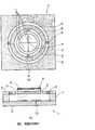
図8(a)は、従来の光通信用光スイッチの構成を示す図、(b)、(c)は(a)の光スイッチの1個のミラーの平面図で、光ビームのミラー面上の位置を示す図である。
80は光スイッチ、81は光ファイバアレイ、82は光ファイバアレイ81の入力ポート、83はコリメートレンズアレイ、84はミラー、85はミラーアレイ、86は光ファイバアレイ81の出力ポート、87は信号光、88はモニタ光分岐手段、89は光検出器、(b)、(c)において、100は光ビームである。
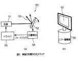
図9は従来の光スキャナの構成を示す図である。
90は光スキャナ、91は光源、92はビームスプリッタ、93はミラー、94は光ビーム、95は光検出器、96は光源91のドライバである。
【0003】
【発明が解決しようとする課題】
従来のミラーは、光の反射機能のみを有する。
例えば、図8に示す対向する2組のミラー84を用いた光スイッチ80においては、光ファイバアレイ81の各チャネルにおける光量をモニタするために、カプラーなどからなるモニタ光分岐手段88により、光を分岐し、光検出器89により光を検出して光強度を測定する必要があり、部品点数が多く、構成が複雑であり、コストが増加する問題があった。
また、コリメートレンズアレイ83等のコリメート系を用いた光スイッチ80では、図8(b)、(c)に示すような、各ミラー84に入射する光ビーム100の位置の検出ができないという問題があった。
また、例えば、図9に示すミラー93を有する光スキャナー90において、光源光量を制御するためには、別の光検出器95を配置して、光源光量をモニタし、フィードハックをかけて、光源91のドライバ96の駆動を制御することにより、光源91の光量を制御する必要があり、部品点数が多く、構成が複雑であり、コストが増加する問題があった。
本発明の目的は、従来のミラーが持つ上記問題を解決し、光ビームやその位置が検出できる手段をミラー自体に設け、部品点数を低減し、構成が簡易で、コストを低減できるミラー、それを用いた光スイッチならびにその製造方法を提供することにある。
【0004】
【課題を解決するための手段】
上記課題を解決するために、本発明のミラーは、ミラー基板面上に光反射層とともに、光検出層を設けることを特徴とし、単に光を反射するだけの従来のミラーと異なるものである。
すなわち、上記課題を解決するため、本発明においては特許請求の範囲に記載するような構成をとる。
つまり、請求項1記載のミラーは、ミラー基板に、光を検出する光検出層と、光を反射する光反射層とが積層され、かつ互いに接して設けられ、前記ミラー基板が光検出機能と光反射機能とを兼ね備えていることを特徴とする。
また、請求項2記載のミラーは、請求項1記載のミラーにおいて、前記ミラー基板の、前記光検出層と前記光反射層とを設けた面の反対面上に、ミラーグラウンド電極を設けたことを特徴とする。
また、請求項3記載のミラーは、請求項1記載のミラーにおいて、前記ミラー基板の、前記光検出層と前記光反射層とを設けた面と同じ側の面上に、ミラーグラウンド電極を設けたことを特徴とする。
また、請求項4記載のミラーは、請求項1、2または3記載のミラーにおいて、上記ミラー基板面上に設けたn型半導体層と、上記n型半導体層上に設けた金属層との金属−半導体界面により形成されるショットキー接合を有し、上記n型半導体層と上記金属層を上記光検出層とし、上記金属層を上記光反射層とすることを特徴とする。
また、請求項5記載のミラーは、請求項1、2または3記載のミラーにおいて、上記ミラー基板面上に設けたp型半導体層と、上記p型半導体層上に設けた金属層との金属−半導体界面により形成されるショットキー接合を有し、上記p型半導体層と上記金属層を上記光検出層とし、上記金属層を上記光反射層とすることを特徴とする。
また、請求項6記載のミラーは、請求項1、2または3記載のミラーにおいて、上記ミラー基板面上に設けたn型半導体層と、上記n型半導体層上に設けた絶縁層と、上記絶縁層上に設けた金属層との金属−絶縁体−半導体界面により形成されるショットキー接合を有し、上記n型半導体層と上記絶縁層と上記金属層を上記光検出層とし、上記金属層を上記光反射層とすることを特徴とする。
また、請求項7記載のミラーは、請求項1、2または3記載のミラーにおいて、上記ミラー基板面上に設けたp型半導体層と、上記p型半導体層上に設けた絶縁層と、上記絶縁層上に設けた金属層との金属−絶縁体−半導体界面により形成されるショットキー接合を有し、上記p型半導体層と上記絶縁層と上記金属層を上記光検出層とし、上記金属層を上記光反射層とすることを特徴とする。
また、請求項8記載のミラーは、請求項1、2または3記載のミラーにおいて、上記ミラー基板面上に設けた光導電性膜を上記光検出層とし、その上に、上記光の検出に必要な光量を透過し、反射率が100%未満の上記光反射層を設けたことを特徴とする。
また、請求項9記載のミラーは、請求項1、2または3記載のミラーにおいて、上記ミラー基板面上に設けたp型半導体層とn型半導体層とにより形成されたp−n接合を有し、上記p型半導体層と上記n型半導体層を上記光検出層とし、その上に、上記光の検出に必要な光量を透過し、反射率が100%未満の上記光反射層を設けたことを特徴とする。
また、請求項10記載のミラーは、請求項1、2または3記載のミラーにおいて、上記ミラー基板面上に設けたp型半導体層、絶縁層、n型半導体層からなるp−i−n構造を上記光検出層とし、その上に、上記光の検出に必要な光量を透過し、反射率が100%未満の上記光反射層を設けたことを特徴とする。
また、請求項11記載のミラーは、請求項1、2または3記載のミラーにおいて、上記ミラー基板面上に設けた光導電性膜を上記光検出層とし、その上に、反射率が100%未満の上記光反射層を設けたことを特徴とする。
また、請求項12記載のミラーは、請求項1、2または3記載のミラーにおいて、上記ミラー基板面上に設けたp型半導体層とn型半導体層とにより形成されたp−n接合を有し、上記p型半導体層と上記n型半導体層を上記光検出層とし、その上に、反射率が100%未満の上記光反射層を設けたことを特徴とする。
また、請求項13記載のミラーは、請求項1、2または3記載のミラーにおいて、上記ミラー基板面上に設けたp型半導体層、絶縁層、n型半導体層からなるp−i−n構造を上記光検出層とし、その上に、反射率が100%未満の上記光反射層を設けたことを特徴とする。
また、請求項14記載のミラーは、請求項1乃至13のいずれか記載のミラーにおいて、上記光検出層が複数個に分割され、当該ミラーに入射する光の位置検出手段を有することを特徴とする。
また、請求項15記載のミラーは、請求項1乃至13のいずれか記載のミラーにおいて、上記光検出層が複数個設けられ、当該ミラーに入射する光の位置検出手段を有することを特徴とする。
また、請求項16記載の光スイッチは、入力用光ファイバアレイと、前記入力用光ファイバアレイからの光ビームを反射させるように配置した請求項1乃至15のいずれか記載の第一のミラーを有する第一のミラーアレイと、前記第一のミラーアレイからの光ビームを反射させる請求項1乃至15のいずれか記載の第二のミラーを有する第二のミラーアレイと、前記第二のミラーアレイからの光ビームを出力する出力用光ファイバアレイを有する光スイッチであって、前記第一のミラーからの前記第二のミラー上における光ビームの位置を検出し、前記第一のミラー上における光ビームが前記第二のミラー上に適切に照射されるように、前記第一のミラーの方向をフィードバック制御する制御装置を有することを特徴とする。
また、請求項17記載の光スイッチの製造方法は、入力用光ファイバアレイと、前記入力用光ファイバアレイからの光ビームを反射させるように配置した請求項1乃至15のいずれか記載の第一のミラーを有する第一のミラーアレイと、前記第一のミラーアレイからの光ビームを反射させる請求項1乃至15のいずれか記載の第二のミラーを有する第二のミラーアレイと、前記第二のミラーアレイからの光ビームを出力する出力用光ファイバアレイを有する光スイッチの製造方法であって、前記第一のミラーの光ビームの位置検出を行い、前記入力用光ファイバアレイの入力ポート側のコリメートレンズアレイと、前記第一のミラーアレイ間の光軸調整を行うことを特徴とする。
本発明のミラーでは、ミラー基板面上に光検出層を設けるので、ミラーに入射する光を検出し、光強度を測定することが可能である。
また、光検出層を複数個設けることにより、ミラー上に入射する光ビームの位置を検出することができる。
また、本発明の光スイッチでは、光検出層によって入射光の強度、位置を検出できるので、外部検出機器を不用とし、ミラーを用いるスイッチング装置等の構成を簡易とし、コストダウンを実現できる。
また、本発明の光スイッチの製造方法では、入力ポート側のコリメートレンズアレイと、第一のミラーアレイ間の光軸が正確に調整された光スイッチを提供できる。
【0005】
【発明の実施の形態】
以下、図面を用いて本発明の実施の形態について詳細に説明する。なお、以下で説明する図面で、同一機能を有するものは同一符号を付け、その繰り返しの説明は省略する。
実施の形態1
図1(a)は、本発明の実施の形態1のミラーの平面図、(b)は(a)の断面図である。
1はミラー、2はミラー基板、3は光検出層、4は光反射層、5はミラー支持基板、6はミラー駆動用電極基板、7はミラー支持構造体、8はねじりばね、9はミラーグラウンド電極、10はミラー駆動用電極、11は4分割光検出面である。
本実施の形態1のミラー1は、ミラー基板2に、光を検出する光検出層3と、光を反射する光反射層4とが積層され、かつ互いに接して設けられ、ミラー基板2が光検出機能と光反射機能とを兼ね備えている。すなわち、ミラー基板2の表面に、面積が均等な4個の光検出層3が分割形成され、その上に、図1(b)に示すように、例えば反射率A%(A<l00)の光反射層4が形成されている。
ミラー1の面に光が入射すると、A%の光が反射され、残りの(100−A)%の光は光検出層3に届き、光検出層3を照射する面積に応じた光検出信号が得られる。
この反射率A%はミラー1の用途、光検出層3の性能により決定される。
光検出信号は、4個の光検出層3と、ミラーグラウンド電極9間で、独立に検出できるので、光ビームの光強度はこれらの4個の光検出信号の合計により測定できる。
また、本実施の形態1のミラー1では、図1(a)に示すように、光検出層3が4個に分割され、当該ミラー1に入射する光の位置検出手段(図示省略)を有する。すなわち、これら4個の光検出層3から取り出される光検出信号の大小を図示しない比較手段により比較することにより、ミラー1の面上の中央からどちらに偏っているかが測定可能であり、光ビームの位置が検出可能である。
本実施の形態1では、ミラーグラウンド電極9をミラー基板2の裏面に形成した場合である。
ミラー基板2はねじりばね8を介して、ミラー基板2外側のミラー支持構造体7と繋がっており、ねじりばね8のねじれにより、ミラー基板2は2軸方向に傾き、ミラー基板2の面を空間的に任意の方向に向けることが可能である。
本実施の形態1では、ミラー基板2の駆動は静電駆動方式であり、ミラー駆動用電極基板6に、平面的に4分割した電極(図1(b)では2個のみ図示)を形成し、それぞれに印加電圧を加えることにより、ミラー基板2とミラー駆動用電極10との間に静電引力が働き、ミラー基板2がミラー駆動用電極基板6に引き付けられ、ねじりばね8のばね力と、この静電引力との平衡点においてつり合い、ミラー基板2の面が所定の位置に偏向する。
【0006】
実施の形態2
図2(a)は、本発明の実施の形態2のミラーの平面図、(b)は(a)の断面図である。
上記実施の形態1においては、ミラーグラウンド電極9をミラー基板2の裏面に形成したが、本実施の形態2においては、図2(a)に示すように、ミラーグラウンド電極9をミラー基板2の表面上の周辺に、すなわち、ミラー基板2の光検出層3と光反射層4とを設けた面と同じ側の面上に形成したものである。その他の構成、作用、効果は上記実施の形態1と同様である。
【0007】
実施の形態3
以下、本実施の形態3のミラー1の製造方法について説明する。
図3(a)〜(g)は、本実施の形態3のミラー1の製造方法を示す工程断面図である。(a)〜(d)はミラー支持基板5の製造工程、(e)、(f)はミラー駆動用電極基板6の製造工程、(g)はミラー支持基板5とミラー駆動用電極基板6との接合工程を示す。
ミラー1の構成は、図1、図2のミラーとほぼ同様である。ここでは、例えばSOI(Silicon On Insulator)基板を用いた例を示す。
まず、図3(a)に示すように、Si層12/SiO2層(中間酸化膜)13/Si層(Si基板)14の3層からなるSOI基板15上に光検出層3を形成し、ミラー形状、電極形状に沿ったパターニングを行う。次に、その上に、光反射層4を形成し、パターニングを行う。
次に、図3(b)に示すように、電極配線16を形成した後、SOI基板15の表面および裏面に、例えばSiO2からなるエッチング用のマスクパターン17を形成する。
次に、図3(c)に示すように、このマスクパターン17をマスクとして、Si層(Si活性層)14からなるミラー基板2と、ねじりばね8の形状加工を、例えば高アスペクト加工用反応性イオンエッチング(Deep RIE(Reactive Ion Etching) またはICP(Induction Coupled Plasma) RIE)で行う。また、マスクパターン17をマスクとして、SOI基板15の下層Si層12を例えばKOH水溶液によりエッチングする。
次に、図3(d)に示すように、ミラー駆動用電極基板6との接合用金属膜(例えば下層からTi/Pt/Au)18を形成し、SOI基板15のSiO2層13と、SiO2からなるマスクパターン(図示省略)をフッ酸で除去し、ねじりばね8により支持された可動ミラー支持基板5が完成する(ミラーグラウンド電極9は図示省略)。
次に、図3(e)に示すように、Si基板からなるミラー駆動用電極基板6に例えば下層からTi/Pt/Auを蒸着して、ミラー駆動用電極10を形成し、そのパターニングを行なう。
次に、図3(f)に示すように、ミラー支持基板5との接合用金属膜および半田膜(金属膜は例えば下層からTi/Pt/Au、半田膜は例えばAuSn)19を蒸着し、パターニングを行なう。
最後に、ミラー支持基板5とミラー駆動用電極基板6とを、上記ハンダを溶かして接合し、ミラー1が完成する。
図1、図2、図3に示した光検出層3としては、例えばミラー基板2面上にn型Si等のn型半導体層を形成し、その上に半透明の薄い金属膜(例えばPt、Au等)を蒸着等により形成した金属−半導体界面のショットキー接合によるものを用いることができる。この場合、この金属層を光反射層4とする。
あるいは、ミラー基板2上にn型Si等のn型半導体層を形成し、その上にSiO2等の絶縁層を形成し、さらにその上に半透明の金属層(例えばPt、Au等)を蒸着等により形成した金属−絶縁体−半導体界面のショットキー接合によるものを用いることができる。この場合、この金属層を光反射層4とする。
このように、ショットキー接合を用いる場合は、光検出層3の一部の金属層と光反射層4とを同一金属層で形成可能であり、製造工程を短縮できる。
なお、光検出層3を構成するn型半導体層に替えて、p型半導体層を用いても良い。
あるいは、ミラー基板2上に光導電性膜を形成したものを用いることができる。この場合、この光導電性膜の上に、光の検出に必要な光量を透過し、反射率が100%未満の光反射層4を設ける。
あるいは、ミラー基板2上に設けたp型半導体層とn型半導体層(どちらが上層、下層でもよい)からなるp−nフォトダイオード層を形成したものを用いることができる。この場合、このp−nフォトダイオード層の上に、光の検出に必要な光量を透過し、反射率が100%未満の光反射層4を設ける。
あるいは、ミラー基板2上に設けたp型半導体層、絶縁層、n型半導体層からなるp−i−nフォトダイオードを形成したものを用いることができる。この場合、このp−i−nフォトダイオード層の上に、光の検出に必要な光量を透過し、反射率が100%未満の光反射層4を設ける。
また、図3の上記製造方法では、シリコンを半導体として用いたが、Ge、SiC、SiGe、AlN、AlP、AlAs、GaN、GaP、GaAs、GaSb、InN、InP、InAs、InSb、ZnO、ZnS、ZnSe、CdS、CdSe、CdTe、HgTe、GaS、GaSe、GaTe、InSe、SnO2、PbS、PbSe、PbTe、Sb2Te3、Bi2Se3、Bi2Te3、InGaAs、AlGaAs等の他の半導体を用いても本発明を実現可能であることは明らかである。
ここで、半導体がシリコンの場合には、精製が容易で、欠陥の少ない単結晶が製作しやすく、また、絶縁膜であるSiO2膜を高品質で形成することが容易であるという利点がある。また、半導体がInGaAs、GaSb、GaAs、InP、InAs、InSb等の場合では、電子移動度が高く、光検出器としての応答速度が速いという利点がある。さらに、半導体が、直接遷移型半導体であるAlN、GaN、GaAs、GaSb、InN、InP、InAs、InSb、ZnO、ZnS、ZnSe、CdS、CdSe、CdTe、HgTe、SnO2等の場合では、同一基板上において、発光ダイオードや、レーザー等の発光する構造を形成することができるという利点がある。
また、図1〜図3の上記実施の形態1〜3においては、光検出層3を4分割したものを示したが、ミラー基板2上に複数個の光検出層3を点対称に、例えばハイブリッド集積して付与した形態でも光ビームの位置検出が可能である。
【0008】
さらに、図1〜図3の上記実施の形態1〜3においては、ミラー基板2の駆動方式として静電引力を用いたが、磁場と電流を利用したローレンツカや電磁力、ピエゾや超音波モーターのような圧電力を用いた駆動方式であっても良いことは言うまでもない。
【0009】
実施の形態4
図4(a)は、本発明の実施の形態4のミラーを用いた光スイッチの構成を示す図、(b)は(a)のミラーの平面図である。
40は光スイッチ、41は光ファイバアレイ、41aは入力用光ファイバアレイ、41bは出力用光ファイバアレイ、42は光ファイバアレイ41aの入力ポート、43a、43bはコリメートレンズアレイ、44a、44bはミラー、45a、45bはミラーアレイ、46は光ファイバアレイ41bの出力ポート、47は信号光、48は制御装置、100は光ビームである。
入力ポート42からの光ビーム100はコリメートレンズアレイ43aを経て、1次ミラーアレイ45aのミラー44a、2次ミラーアレイ45bのミラー44bで偏向され、所望の出力ポート46ヘ誘導される。このとき、光ビーム100を偏向すると同時に、光検出層3を有するミラー44aまたは44b面上で信号光47の光を検出し、光強度を測定できるので、出カポート46での信号光強度のモニタ、すなわち、モニタ光分岐手段(図8の88)、光検出器(図8の89)は不要である。また、本実施の形態4では、光検出層3を4個に分割した4分割光検出機能により、ミラー44aまたは44b上への光ビームの位置検出が可能で、この信号をミラー44aまたは44bの位置制御に用いることもできる。
一例として、光検出層3を4個に分割した4分割光検出機能により、2次ミラーアレイ45b上のミラー44b上における光ビームの位置検出が可能で、この信号を解析して、光ビームが2次ミラーアレイ45b上のミラー44bの中心に適切に照射されるように、1次ミラーアレイ上45a上のミラー44aの方向をフィードバック制御することもできる。また、1次ミラーアレイ45a上のミラー44aにおいて、同様の光ビームの位置検出を行うこともでき、この信号を解析して、上記光スイッチ製作時において、入力ポート42側のコリメートレンズアレイ43aと1次ミラーアレイ45a間の光軸調整に用いることができる。
【0010】
すなわち、本実施の形態4の光スイッチ40は、入力用光ファイバアレイ41aと、入力用光ファイバアレイ41aからの光ビームを反射させるように配置した実施の形態1〜3の第一のミラー44aを有する第一のミラーアレイ45aと、第一のミラーアレイ45aからの光ビームを反射させる実施の形態1〜3の第二のミラー44bを有する第二のミラーアレイ45bと、第二のミラーアレイ45bからの光ビームを出力する出力用光ファイバアレイ41bを有する光スイッチ40であって、第一のミラー44aからの第二のミラー44b上における光ビームの位置を検出し、第一のミラー44a上における光ビームが第二のミラー44b上に適切に照射されるように、第一のミラー44aの方向をフィードバック制御する制御装置48を有する。
このような構成により、光検出層3によって入射光の強度、位置を検出できるので、外部検出機器を不用とし、ミラーを用いるスイッチング装置等の構成を簡易とし、コストダウンを実現できる。
また、本実施の形態4の光スイッチ40の製造方法は、入力用光ファイバアレイ41aと、入力用光ファイバアレイ41aからの光ビームを反射させるように配置した実施の形態1〜3の第一のミラー44aを有する第一のミラーアレイ45aと、第一のミラーアレイ45aからの光ビームを反射させる実施の形態1〜3の第二のミラー44bを有する第二のミラーアレイ45bと、第二のミラーアレイ45bからの光ビームを出力する出力用光ファイバアレイ41bを有する光スイッチ40の製造方法であって、第一のミラー44aの光ビームの位置検出を行い、入力用光ファイバアレイ41aの入力ポート42側のコリメートレンズアレイ43aと、第一のミラーアレイ45a間の光軸調整を行う。
このような構成により、入力ポート42側のコリメートレンズアレイ43aと、第一のミラーアレイ45a間の光軸が正確に調整された光スイッチ40を提供できる。
【0011】
実施の形態5
図5(a)は、本発明の実施の形態5のミラーを用いた光スキャナの構成を示す図、(b)は(a)のミラーの斜視図である。
50は光スキャナ、51は光源、52はミラー、53は光ビーム、54は光強度(光量)検出器、55は光源51のドライバ、(b)において、56はミラー駆動源である。
光源51からの光ビーム53がミラー52の面で反射され、任意の方向に偏向される。ミラー52の面で光ビーム53の偏向を行うと同時に、ミラー52に設けた光検出層3により光を検出し、光強度検出器54により光強度の検出が可能であるので、従来必要であった光ビーム53を分岐させるビームスプリッタ(図9の92)や別装置として光検出器(図9の95)を用意する必要がない。
【0012】
実施の形態6
図6(a)は、本発明の実施の形態6のミラーの光検出層3からの光信号(光電流)取り出し用配線の構成を示す図、(b)は光検出層3にフォトダイオード等の光起電力層を用いた場合の信号検出回路図、(c)は光検出層3に光導電性膜を用いた場合の信号検出回路図である。
(a)において、1はミラー、3は光検出層(光検出層3の上に光反射層4が形成されている)、8はねじりばね、60は光信号取り出し用配線、9はミラーグラウンド電極、61はミラーグラウンド配線、(b)において、62は光、63はフォトダイオード、64はアノード、65はカソード、66はオペアンプ、(c)において、67は光導電性膜、68は外部電源、69は固定抵抗である。
本実施の形態6は、最もシンプルな1軸ミラーで、1個のアノードと1個のカソードを有する構成例である。図6(a)に示すように、光信号取り出し用配線60とその光信号取り出し用電極パッド(アノード)64、並びにミラーグラウンド配線61とそのミラーグラウンド電極パッド(カソード)65を形成して、各電極パッド64、65からワイヤボンディング実装により外部へ取り出す。
【0013】
光検出層3にフォトダイオード等の光起電力層を用いた場合は、図6(b)に示すように、オペアンプ66等を用いて光電流を電圧出力として取り出す。
光検出層3に光導電性膜を用いた場合は、図6(c)に示すように、光照射により抵抗が変化するので、外部電源68から供給される電流の変化を別の固定抵抗69を介して取り出す。
【0014】
実施の形態7
図7(a)は、本発明の実施の形態7のミラーの光検出層3からの光信号(光電流)取り出し用配線の構成を示す図、(b)はその信号検出回路図である。
(a)において、71a〜71dは光信号取り出し用配線、72a、72bはミラーグラウンド配線、(b)において、73a〜73dは光、74a〜74dはフォトダイオード、75a〜75dはアノード、76はカソード、77a〜77dはオペアンプである。
本実施の形態7は、図7(a)に示すように、フォトダイオード等の光起電力層を用いた光検出層3が4分割された2軸ミラーで、4個のアノードと1個のカソードを有する構成例である。
このように分割した光検出層3を備えたミラー70は、図7(b)に示すように、各光検出層3に対応した検出回路を構成し(グラウンドは共通)、それぞれの光信号出力Vout1〜Vout4を比較し、光ビームの偏光状況を判断することが可能である。
以上説明したように、上記実施の形態1〜7では、ミラーに反射機能に加えて、光検出機能を集積しているので、従来のミラーでは知り得なかった光ビームの光強度を他の検出器無しで測定できる。また、光検出層3を複数個に分割する多分割光検出構造、または例えば多数個のフォトダイオードチップをボンディングする等、多数の光検出部分を持つ構造にすることで、光ビームの位置検出も可能となる。また、光ビームの偏向と光検出の両方が必要な装置においては、従来必要であった検出器等の部品を用いる必要がなく、ミラーのみで構成できるため、装置を構成する場合において部品点数を削減でき、大きく経済化を図ることができる。
以上本発明を実施の形態に基づいて具体的に説明したが、本発明は上記実施の形態に限定されるものではなく、その要旨を逸脱しない範囲において種々変更可能であることは勿論である。
【0015】
【発明の効果】
以上説明したように、本発明のミラーによれば、従来のミラーでは知り得なかった光ビームの光強度を他の検出器無しで測定できる。また、光検出層を複数個設けることにより光ビームの位置検出も可能となる。また、光ビームの偏向と光検出の両方が必要な装置においては、従来必要であった検出器等の部品を用いる必要がなく、ミラーのみで構成できるため、装置を構成する場合において部品点数を削減でき、大きく経済化を図ることができる。また、本発明の光スイッチによれば、光検出層によって入射光の強度、位置を検出できるので、外部検出機器を不用とし、ミラーを用いるスイッチング装置等の構成を簡易とし、コストダウンを実現できる。また、本発明の光スイッチの製造方法によれば、入力ポート側のコリメートレンズアレイと、第一のミラーアレイ間の光軸が正確に調整された光スイッチを提供できる。
【図面の簡単な説明】
【図1】(a)は本発明の実施の形態1のミラーの平面図、(b)は(a)の断面図である。
【図2】(a)は本発明の実施の形態2のミラーの平面図、(b)は(a)の断面図である。
【図3】(a)〜(g)は本実施の形態3のミラーの製造方法を示す工程断面図である。
【図4】(a)は本発明の実施の形態4のミラーを用いた光スイッチの構成を示す図、(b)は(a)のミラーの平面図である。
【図5】(a)は本発明の実施の形態5のミラーを用いた光スキャナの構成を示す図、(b)は(a)のミラーの斜視図である。
【図6】(a)は本発明の実施の形態6のミラーの光検出層からの光信号取り出し用配線の構成を示す図、(b)は光検出層にフォトダイオード等の光起電力層を用いた場合の信号検出回路図、(c)は光検出層に光導電性膜を用いた場合の信号検出回路図である。
【図7】(a)は本発明の実施の形態7のミラーの光検出層からの光信号取り出し用配線の構成を示す図、(b)はその信号検出回路図である。
【図8】(a)は従来の光通信用光スイッチの構成を示す図、(b)、(c)は(a)の光スイッチの1個のミラーの平面図で、光ビームのミラー面上の位置を示す図である。
【図9】従来の光スキャナの構成を示す図である。
【符号の説明】
1…ミラー、2…ミラー基板、3…光検出層、4…光反射層、5…ミラー支持基板、6…ミラー駆動用電極基板、7…ミラー支持構造体、8…ねじりばね、9…ミラーグラウンド電極、10…ミラー駆動用電極、11…4分割光検出面、12…Si層、13…SiO2層、14…Si層、15…SOI基板、16…電極配線、17…マスクパターン、18…接合用金属膜、19…接合用金属膜および半田膜、40…光スイッチ、41、41a、41b…光ファイバアレイ、42…入力ポート、43a、43b…コリメートレンズアレイ、44a、44b…ミラー、45a、45b…ミラーアレイ、46…出力ポート、47…信号光、48…制御装置、50…光スキャナ、51…光源、52…ミラー、53…光ビーム、54…光強度検出器、55…ドライバ、56…ミラー駆動源、60…光信号取り出し用配線、61…ミラーグラウンド配線、62…光、63…フォトダイオード、64…アノード、65…カソード、66…オペアンプ、67…光導電性膜、68…外部電源、69…固定抵抗、71a〜71d…光信号取り出し用配線、72a、72b…ミラーグラウンド配線、73a〜73d…光、74a〜74dフォトダイオード、75a〜75d…アノード、76…カソード、77a〜77d…オペアンプ、80…光スイッチ、81…光ファイバアレイ、82…入力ポート、83…コリメートレンズアレイ、84…ミラー、85…ミラーアレイ、86…出力ポート、87…信号光、88…モニタ光分岐手段、89…光検出器、90…光スキャナ、91…光源、92…ビームスプリッタ、93…ミラー、94…光ビーム、95…光検出器、96…ドライバ、100…光ビーム。[0001]
BACKGROUND OF THE INVENTION
The present invention relates to a mirror for an optical switch for optical communication, a mirror such as a beam deflection mirror used in an optical sensor, a light reflection type display, an optical scanner, etc., an optical switch using the same, and a method for manufacturing the same.
[0002]
[Prior art]
FIG. 8A is a diagram showing a configuration of a conventional optical switch for optical communication, and FIGS. 8B and 8C are plan views of one mirror of the optical switch of FIG. 8A on the mirror surface of the light beam. FIG.
80 is an optical switch, 81 is an optical fiber array, 82 is an input port of the
FIG. 9 is a diagram showing a configuration of a conventional optical scanner.
[0003]
[Problems to be solved by the invention]
A conventional mirror has only a light reflecting function.
For example, in the
Further, in the
Further, for example, in the
An object of the present invention is to solve the above-mentioned problems of conventional mirrors, and to provide a means for detecting the light beam and its position in the mirror itself, to reduce the number of parts, to simplify the configuration, and to reduce the cost. It is an object to provide an optical switch using the above and a manufacturing method thereof.
[0004]
[Means for Solving the Problems]
In order to solve the above problems, the mirror of the present invention is characterized in that a light detection layer and a light detection layer are provided on the mirror substrate surface, which is different from a conventional mirror that merely reflects light.
That is, in order to solve the above problems, the present invention adopts a configuration as described in the claims.
That is, the mirror according to
According to a second aspect of the present invention, in the mirror according to the first aspect, a mirror ground electrode is provided on a surface of the mirror substrate opposite to the surface on which the light detection layer and the light reflection layer are provided. It is characterized by.
The mirror according to
According to a fourth aspect of the present invention, there is provided the mirror according to the first, second, or third aspect, wherein the n-type semiconductor layer provided on the mirror substrate surface and the metal layer provided on the n-type semiconductor layer are metal. A Schottky junction formed by a semiconductor interface, wherein the n-type semiconductor layer and the metal layer are the photodetecting layer, and the metal layer is the light reflecting layer.
According to a fifth aspect of the present invention, in the mirror according to the first, second, or third aspect, the metal is composed of a p-type semiconductor layer provided on the mirror substrate surface and a metal layer provided on the p-type semiconductor layer. A Schottky junction formed by a semiconductor interface, wherein the p-type semiconductor layer and the metal layer are the photodetection layer, and the metal layer is the light reflection layer.
The mirror according to
A mirror according to
The mirror according to
The mirror according to
The mirror according to
The mirror according to
According to a twelfth aspect of the present invention, the mirror according to the first, second, or third aspect has a pn junction formed by a p-type semiconductor layer and an n-type semiconductor layer provided on the mirror substrate surface. The p-type semiconductor layer and the n-type semiconductor layer are used as the light detection layer, and the light reflection layer having a reflectance of less than 100% is provided thereon.
A mirror according to a thirteenth aspect is the mirror according to the first, second, or third aspect, wherein the pin structure includes a p-type semiconductor layer, an insulating layer, and an n-type semiconductor layer provided on the mirror substrate surface. Is the light detection layer, and the light reflection layer having a reflectance of less than 100% is provided thereon.
A mirror according to
A mirror according to a fifteenth aspect is the mirror according to any one of the first to thirteenth aspects, wherein a plurality of the light detection layers are provided, and a position detecting unit for light incident on the mirror is provided. .
The optical switch according to
The optical switch manufacturing method according to claim 17 is the first optical fiber array according to any one of
In the mirror of the present invention, since the light detection layer is provided on the mirror substrate surface, it is possible to detect light incident on the mirror and measure the light intensity.
Further, by providing a plurality of light detection layers, the position of the light beam incident on the mirror can be detected.
In the optical switch of the present invention, since the intensity and position of incident light can be detected by the light detection layer, an external detection device is not required, the configuration of a switching device using a mirror is simplified, and cost reduction can be realized.
Further, according to the method for manufacturing an optical switch of the present invention, it is possible to provide an optical switch in which the optical axis between the collimating lens array on the input port side and the first mirror array is accurately adjusted.
[0005]
DETAILED DESCRIPTION OF THE INVENTION
Hereinafter, embodiments of the present invention will be described in detail with reference to the drawings. In the drawings described below, components having the same function are denoted by the same reference numerals, and repeated description thereof is omitted.
FIG. 1A is a plan view of a mirror according to
1 is a mirror, 2 is a mirror substrate, 3 is a light detection layer, 4 is a light reflection layer, 5 is a mirror support substrate, 6 is a mirror drive electrode substrate, 7 is a mirror support structure, 8 is a torsion spring, and 9 is a mirror. A ground electrode, 10 is a mirror driving electrode, and 11 is a quadrant light detection surface.
The
When light is incident on the surface of the
The reflectance A% is determined by the use of the
Since the light detection signal can be detected independently between the four
Further, in the
In the first embodiment, the
The
In the first embodiment, the
[0006]
2A is a plan view of a mirror according to
In the first embodiment, the
[0007]
Hereinafter, the manufacturing method of the
3A to 3G are process cross-sectional views illustrating a method for manufacturing the
The configuration of the
First, as shown in FIG. 3A, the
Next, as shown in FIG. 3B, after the
Next, as shown in FIG. 3C, using the mask pattern 17 as a mask, the
Next, as shown in FIG. 3D, a metal film (for example, Ti / Pt / Au from the lower layer) 18 for bonding to the mirror driving
Next, as shown in FIG. 3E, for example, Ti / Pt / Au is vapor-deposited on the mirror driving
Next, as shown in FIG. 3 (f), a metal film and a solder film for bonding to the mirror support substrate 5 (a metal film, for example, Ti / Pt / Au from a lower layer, and a solder film, for example, AuSn) 19 are vapor-deposited. Patterning is performed.
Finally, the
As the
Alternatively, an n-type semiconductor layer such as n-type Si is formed on the
Thus, when a Schottky junction is used, a part of the metal layer of the
Note that a p-type semiconductor layer may be used instead of the n-type semiconductor layer constituting the
Or what formed the photoconductive film | membrane on the mirror board |
Or what formed the pn photodiode layer which consists of a p-type semiconductor layer and n-type semiconductor layer (which may be an upper layer or a lower layer) provided on the
Or what formed the p-i-n photodiode which consists of a p-type semiconductor layer provided on the
In the manufacturing method of FIG. 3, silicon is used as a semiconductor, but Ge, SiC, SiGe, AlN, AlP, AlAs, GaN, GaP, GaAs, GaSb, InN, InP, InAs, InSb, ZnO, ZnS, ZnSe, CdS, CdSe, CdTe, HgTe, GaS, GaSe, GaTe, InSe, SnO2 , PbS, PbSe, PbTe, Sb2 Te3 , Bi2 Se3 , Bi2 Te3 It is apparent that the present invention can be realized even if other semiconductors such as InGaAs and AlGaAs are used.
Here, when the semiconductor is silicon, it is easy to purify and a single crystal with few defects can be easily manufactured.2 There is an advantage that it is easy to form a film with high quality. Further, when the semiconductor is InGaAs, GaSb, GaAs, InP, InAs, InSb, or the like, there are advantages that electron mobility is high and response speed as a photodetector is fast. Further, the semiconductor is a direct transition type semiconductor such as AlN, GaN, GaAs, GaSb, InN, InP, InAs, InSb, ZnO, ZnS, ZnSe, CdS, CdSe, CdTe, HgTe, SnO.2 In such a case, there is an advantage that a light emitting diode or a light emitting structure such as a laser can be formed on the same substrate.
In the first to third embodiments shown in FIGS. 1 to 3, the
[0008]
Further, in
[0009]
FIG. 4A is a diagram showing a configuration of an optical switch using a mirror according to
40 is an optical switch, 41 is an optical fiber array, 41a is an input optical fiber array, 41b is an output optical fiber array, 42 is an input port of the optical fiber array 41a, 43a and 43b are collimating lens arrays, and 44a and 44b are mirrors. 45a and 45b are mirror arrays, 46 is an output port of the
The
As an example, the position of the light beam on the mirror 44b on the secondary mirror array 45b can be detected by the four-split light detection function in which the
[0010]
In other words, the
With such a configuration, since the intensity and position of incident light can be detected by the
Further, the manufacturing method of the
With such a configuration, it is possible to provide the
[0011]
FIG. 5A is a diagram showing a configuration of an optical scanner using the mirror according to the fifth embodiment of the present invention, and FIG. 5B is a perspective view of the mirror of FIG.
50 is an optical scanner, 51 is a light source, 52 is a mirror, 53 is a light beam, 54 is a light intensity (light quantity) detector, 55 is a driver of the
The
[0012]
FIG. 6A is a diagram showing the configuration of the optical signal (photocurrent) extraction wiring from the
In (a), 1 is a mirror, 3 is a light detection layer (a
The sixth embodiment is a simplest uniaxial mirror and has a configuration having one anode and one cathode. As shown in FIG. 6A, an optical
[0013]
When a photovoltaic layer such as a photodiode is used for the
When a photoconductive film is used for the
[0014]
FIG. 7A is a diagram showing a configuration of an optical signal (photocurrent) extraction wiring from the
In (a), 71a to 71d are optical signal extraction wirings, 72a and 72b are mirror ground wirings, and in (b), 73a to 73d are light, 74a to 74d are photodiodes, 75a to 75d are anodes, and 76 is a cathode. , 77a to 77d are operational amplifiers.
As shown in FIG. 7A, the seventh embodiment is a biaxial mirror in which a
As shown in FIG. 7B, the
As described above, in the first to seventh embodiments, since the light detection function is integrated in the mirror in addition to the reflection function, the light intensity of the light beam, which cannot be known by the conventional mirror, is detected by other methods. Can be measured without a vessel. In addition, the
Although the present invention has been specifically described above based on the embodiment, the present invention is not limited to the above-described embodiment, and it is needless to say that various changes can be made without departing from the scope of the invention.
[0015]
【The invention's effect】
As described above, according to the mirror of the present invention, it is possible to measure the light intensity of a light beam that could not be known by a conventional mirror without using another detector. Further, the position of the light beam can be detected by providing a plurality of light detection layers. In addition, in an apparatus that requires both light beam deflection and light detection, it is not necessary to use parts such as detectors that have been required in the past. It can be reduced and the economy can be greatly improved. In addition, according to the optical switch of the present invention, since the intensity and position of incident light can be detected by the light detection layer, an external detection device is not required, the configuration of a switching device using a mirror can be simplified, and cost reduction can be realized. . Further, according to the method for manufacturing an optical switch of the present invention, it is possible to provide an optical switch in which the optical axis between the collimating lens array on the input port side and the first mirror array is accurately adjusted.
[Brief description of the drawings]
1A is a plan view of a mirror according to a first embodiment of the present invention, and FIG. 1B is a cross-sectional view of FIG.
2A is a plan view of a mirror according to a second embodiment of the present invention, and FIG. 2B is a cross-sectional view of FIG.
FIGS. 3A to 3G are process cross-sectional views illustrating a manufacturing method of a mirror according to a third embodiment.
4A is a diagram showing a configuration of an optical switch using a mirror according to a fourth embodiment of the present invention, and FIG. 4B is a plan view of the mirror in FIG. 4A.
5A is a diagram showing a configuration of an optical scanner using a mirror according to a fifth embodiment of the present invention, and FIG. 5B is a perspective view of the mirror of FIG. 5A.
FIG. 6A is a diagram showing a configuration of an optical signal extraction wiring from a photodetection layer of a mirror according to a sixth embodiment of the present invention, and FIG. (C) is a signal detection circuit diagram when a photoconductive film is used for the photodetection layer.
7A is a diagram showing a configuration of an optical signal extraction wiring from a photodetection layer of a mirror according to a seventh embodiment of the present invention, and FIG. 7B is a signal detection circuit diagram thereof.
8A is a diagram showing a configuration of a conventional optical switch for optical communication, and FIGS. 8B and 8C are plan views of one mirror of the optical switch of FIG. It is a figure which shows the upper position.
FIG. 9 is a diagram illustrating a configuration of a conventional optical scanner.
[Explanation of symbols]
DESCRIPTION OF
Claims (17)
Translated fromJapanesePriority Applications (1)
| Application Number | Priority Date | Filing Date | Title |
|---|---|---|---|
| JP2002039752AJP4040324B2 (en) | 2001-10-24 | 2002-02-18 | Mirror, optical switch using the same, and manufacturing method thereof |
Applications Claiming Priority (3)
| Application Number | Priority Date | Filing Date | Title |
|---|---|---|---|
| JP2001-326333 | 2001-10-24 | ||
| JP2001326333 | 2001-10-24 | ||
| JP2002039752AJP4040324B2 (en) | 2001-10-24 | 2002-02-18 | Mirror, optical switch using the same, and manufacturing method thereof |
Publications (2)
| Publication Number | Publication Date |
|---|---|
| JP2003202418A JP2003202418A (en) | 2003-07-18 |
| JP4040324B2true JP4040324B2 (en) | 2008-01-30 |
Family
ID=27666448
Family Applications (1)
| Application Number | Title | Priority Date | Filing Date |
|---|---|---|---|
| JP2002039752AExpired - Fee RelatedJP4040324B2 (en) | 2001-10-24 | 2002-02-18 | Mirror, optical switch using the same, and manufacturing method thereof |
Country Status (1)
| Country | Link |
|---|---|
| JP (1) | JP4040324B2 (en) |
Families Citing this family (8)
| Publication number | Priority date | Publication date | Assignee | Title |
|---|---|---|---|---|
| JP4396299B2 (en)* | 2004-02-09 | 2010-01-13 | 日立金属株式会社 | Mirror system and optical switch |
| JP4627627B2 (en) | 2004-03-31 | 2011-02-09 | 富士通株式会社 | Micromirror element and optical switch |
| JP2005326620A (en)* | 2004-05-14 | 2005-11-24 | Fujitsu Ltd | Micro mirror element |
| JP5221037B2 (en) | 2005-01-05 | 2013-06-26 | 日本電信電話株式会社 | Mirror device |
| JP2010101627A (en)* | 2008-10-21 | 2010-05-06 | Murata Mfg Co Ltd | Ultraviolet light measuring device, compact case, and electronic device |
| JP5573212B2 (en)* | 2010-02-08 | 2014-08-20 | 株式会社ニコン | Spatial light modulation element, manufacturing method of spatial light modulation element, illumination light generator and exposure apparatus |
| US9213142B2 (en) | 2013-11-21 | 2015-12-15 | Huawei Technologies Co., Ltd. | Device and method for micro-electro-mechanical-system photonic switch |
| US9983403B2 (en) | 2014-10-03 | 2018-05-29 | Huawei Technologies Co., Ltd. | Device and method for micro-electro-mechanical-system photonic switch |
- 2002
- 2002-02-18JPJP2002039752Apatent/JP4040324B2/ennot_activeExpired - Fee Related
Also Published As
| Publication number | Publication date |
|---|---|
| JP2003202418A (en) | 2003-07-18 |
Similar Documents
| Publication | Publication Date | Title |
|---|---|---|
| US6246708B1 (en) | Semiconductor laser with associated electronic components integrally formed therewith | |
| US6054335A (en) | Fabrication of scanning III-V compound light emitters integrated with Si-based actuators | |
| KR100809413B1 (en) | Vertical cavity surface emitting laser having monitoring photodiode and method of fabrication the same | |
| CN100367069C (en) | Micromirror elements and optical switches | |
| US20030109142A1 (en) | Integrated photodetector for VCSEL feedback control | |
| JP4040324B2 (en) | Mirror, optical switch using the same, and manufacturing method thereof | |
| JP3058077B2 (en) | Semiconductor light emitting and receiving device | |
| US6633598B1 (en) | Semiconductor laser device, and image forming apparatus | |
| JP2005217147A (en) | Light emitting / receiving element array, optical module, and optical transmission device | |
| EP1195863B1 (en) | Micro-lens built-in vertical cavity surface emitting laser | |
| JPH11121878A (en) | Integrated semiconductor laser, detector structure, and its forming method | |
| US20040146298A1 (en) | Optical switch | |
| JP3610235B2 (en) | Surface light emitting device | |
| JP2539089B2 (en) | Semiconductor laser amplifier and semiconductor laser amplifier | |
| JP2020129588A (en) | Surface emission laser module, light source device, and detection device | |
| JP2013118421A (en) | Laser assembly with integrated photodiode | |
| US20020131145A1 (en) | Structure and method for forming a high efficiency electro-optics device | |
| US7067854B2 (en) | Optical receiver | |
| US4978208A (en) | Photoelectronic diode spatial light modulator and eye protection goggles incorporating the same | |
| US6567448B1 (en) | Scanning III-V compound light emitters integrated with Si-based actuators | |
| JPH09223816A (en) | Semiconductor light receiving element | |
| JPH06103597A (en) | Integrated optical pickup | |
| Deri et al. | Ultra-compact monolithic integration of polarization diversity waveguide photodiodes | |
| JP4387485B2 (en) | Light source device for emitting evanescent light | |
| US20080291953A1 (en) | Light-Emitting System Provided with an Integrated Control Photosensor and a Method for Producing Said System |
Legal Events
| Date | Code | Title | Description |
|---|---|---|---|
| A977 | Report on retrieval | Free format text:JAPANESE INTERMEDIATE CODE: A971007 Effective date:20051227 | |
| A131 | Notification of reasons for refusal | Free format text:JAPANESE INTERMEDIATE CODE: A131 Effective date:20070306 | |
| A521 | Request for written amendment filed | Free format text:JAPANESE INTERMEDIATE CODE: A523 Effective date:20070420 | |
| TRDD | Decision of grant or rejection written | ||
| A01 | Written decision to grant a patent or to grant a registration (utility model) | Free format text:JAPANESE INTERMEDIATE CODE: A01 Effective date:20071106 | |
| A61 | First payment of annual fees (during grant procedure) | Free format text:JAPANESE INTERMEDIATE CODE: A61 Effective date:20071107 | |
| FPAY | Renewal fee payment (event date is renewal date of database) | Free format text:PAYMENT UNTIL: 20101116 Year of fee payment:3 | |
| R150 | Certificate of patent or registration of utility model | Free format text:JAPANESE INTERMEDIATE CODE: R150 | |
| FPAY | Renewal fee payment (event date is renewal date of database) | Free format text:PAYMENT UNTIL: 20101116 Year of fee payment:3 | |
| FPAY | Renewal fee payment (event date is renewal date of database) | Free format text:PAYMENT UNTIL: 20111116 Year of fee payment:4 | |
| FPAY | Renewal fee payment (event date is renewal date of database) | Free format text:PAYMENT UNTIL: 20111116 Year of fee payment:4 | |
| FPAY | Renewal fee payment (event date is renewal date of database) | Free format text:PAYMENT UNTIL: 20121116 Year of fee payment:5 | |
| FPAY | Renewal fee payment (event date is renewal date of database) | Free format text:PAYMENT UNTIL: 20121116 Year of fee payment:5 | |
| FPAY | Renewal fee payment (event date is renewal date of database) | Free format text:PAYMENT UNTIL: 20131116 Year of fee payment:6 | |
| LAPS | Cancellation because of no payment of annual fees |