JP4040027B2 - Rear light source device - Google Patents
Rear light source deviceDownload PDFInfo
- Publication number
- JP4040027B2 JP4040027B2JP2004059047AJP2004059047AJP4040027B2JP 4040027 B2JP4040027 B2JP 4040027B2JP 2004059047 AJP2004059047 AJP 2004059047AJP 2004059047 AJP2004059047 AJP 2004059047AJP 4040027 B2JP4040027 B2JP 4040027B2
- Authority
- JP
- Japan
- Prior art keywords
- light
- light emitting
- row
- adjacent
- light guide
- Prior art date
- Legal status (The legal status is an assumption and is not a legal conclusion. Google has not performed a legal analysis and makes no representation as to the accuracy of the status listed.)
- Expired - Fee Related
Links
Images


Landscapes
- Light Guides In General And Applications Therefor (AREA)
- Liquid Crystal (AREA)
- Planar Illumination Modules (AREA)
Description
Translated fromJapanese本発明は、液晶表示装置に使用する背面光源装置に関するものである。 The present invention relates to a back light source device used for a liquid crystal display device.
液晶表示装置に使用される背面光源装置において、従来、半導体発光素子を1列に並べて、これらの半導体発光素子から出射される光を導光板で、導光板拡散板へ導光していた。 Conventionally, in a back light source device used for a liquid crystal display device, semiconductor light emitting elements are arranged in a line, and light emitted from these semiconductor light emitting elements is guided to a light guide plate diffusion plate by a light guide plate.
例えば、特許文献1(特許第2917866号)に開示された背面光源装置では、LEDが支持体を介して固定されている。このように支持体に埋め込まれたLEDを光源とする場合、支持体は透明な材料を選択し、LEDが装着された透明な支持体の端面と、導光板の端面とを密着、あるいは接着剤を介して接着することにより面光源が完成される。 For example, in the rear light source device disclosed in Patent Document 1 (Japanese Patent No. 2917866), the LED is fixed via a support. When the LED embedded in the support is used as a light source, a transparent material is selected for the support, and the end surface of the transparent support on which the LED is mounted and the end surface of the light guide plate are in close contact with each other, or an adhesive. The surface light source is completed by adhering via the surface.
上記特許文献1に記載された従来の背面光源装置では、導光板の側面の幅に対向して並べられる半導体発光素子の数が限られているので、導光板へ注入できる光の総量には限界がある。したがって、半導体発光素子を使用する背面光源装置の輝度向上には問題があった。 In the conventional rear light source device described in Patent Document 1, since the number of semiconductor light emitting elements arranged facing the width of the side surface of the light guide plate is limited, the total amount of light that can be injected into the light guide plate is limited. There is. Therefore, there has been a problem in improving the luminance of the back light source device using the semiconductor light emitting element.
また、半導体発光素子が点光源であることに起因する明るさのむらが生じたり、赤、緑及び青の3原色を混合して使用する場合は、各原色光の到達量の差から、色むらが生じる不都合があった。 In addition, when the semiconductor light emitting element is a point light source, brightness unevenness occurs, or when the three primary colors of red, green, and blue are mixed and used, the color unevenness is caused by the difference in the arrival amount of each primary color light. There was an inconvenience that occurred.
本発明は、上述のような課題を解消するためになされたもので、高輝度で、むらの無い背面光源装置を実現しようとするものである。 The present invention has been made to solve the above-described problems, and an object of the present invention is to realize a back light source device having high brightness and no unevenness.
本発明は、半導体発光素子を光源とし、この光源からの出射光を一つの導光拡散板で拡散する背面光源装置において、
複数列の半導体発光素子と、
各々が、前記複数列の半導体発光素子の各列に対応する複数の導光板であり、対応する列の半導体発光素子から出射された光のみを前記導光拡散板へ導く前記複数の導光板とを有し、
前記複数列の半導体発光素子の隣接する2つの列において、第1の列中で隣接する発光素子間に、第2の列中の発光素子が配列されることを特徴とする。
The present invention uses a semiconductor light emitting element as a light source, and in a back light source device that diffuses light emitted from the light source with a single light guide diffusion plate,
A plurality of rows of semiconductor light emitting devices;
Each said a plurality of rows plurality of light guide plates corresponding to each columnof the semiconductor light emitting device, and a correspondingplurality of light guide platesonly light emitted from the semiconductor light emitting element row leading to the light diffusing plateI have a,
In two adjacent columns of the plurality of columns of semiconductor light emitting elements, the light emitting elements in the second column are arranged between the adjacent light emitting elements in the first column.
本発明は、複数列の半導体発光素子から出射された光を、各々の列に対応する導光板により、1つの導光拡散板へ入射して合成するので、高輝度で、明るさにむらのない背面光源装置が実現できる。 In the present invention, light emitted from a plurality of rows of semiconductor light emitting elements is made incident on one light guide diffusion plate by a light guide plate corresponding to each row, so that it has high brightness and uneven brightness. No back light source device can be realized.
以下、本発明を、実施の形態を示す図面に基づいて具体的に説明する。
実施の形態1.
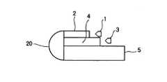
図1は、本発明の実施の形態1に係わる背面光源装置の側面を示すものである。同図において、各半導体発光素子列1、3中の半導体発光素子は、紙面に垂直な方向に整列している。半導体発光素子列1から出射された光が導光板2へ入射し、更に導光拡散板5で導光及び拡散される。一方、半導体発光素子列3から出射された光は、導光板4で導光され、更に導光拡散板5で導光及び拡散される。導光拡散板5で導光及び拡散された光は、導光拡散板5の表面に対して垂直な方向(図中下向き)へ光が出射される。Hereinafter, the present invention will be specifically described with reference to the drawings illustrating embodiments.
Embodiment 1 FIG.
FIG. 1 shows a side surface of a back light source device according to Embodiment 1 of the present invention. In the figure, the semiconductor light emitting elements in each of the semiconductor light
上記構成により、2列の半導体発光素子から出射された光が、導光拡散板5で混合されることで、光の量が増し、高輝度の背面光源装置が実現される。また、この構成では2列の半導体発光素子としたが、2列以上の半導体発光素子列とこれに対応して2枚以上の導光板にて構成しても、同様の効果が得られる。 With the above configuration, the light emitted from the two rows of semiconductor light emitting elements is mixed by the light
実施の形態2.
図2は、本発明の実施の形態2に係わる背面光源装置を示す。実施の形態2では、導光板2に比較して、導光板6は薄い構造となっている。このような構成では、2つの半導体発光素子列1、3から出射される光が、各列に対応する導光板へ入射するが、厚い導光板2では入射量が多く、薄い導光板6では入射量が少なくなる。このため、厚い導光板2に対応する半導体発光素子の発光が少なくても、導光拡散板5への入射光が均一の光となり、明るさにむらの少ない背面光源装置を実現できる。
FIG. 2 shows a back light source device according to Embodiment 2 of the present invention. In the second embodiment, the
実施の形態3.
図3は、この発明の実施の形態3に係わる背面光源装置を示す。実施の形態3では、導光板2に比較して導光板7が長い構造となっている。上記構成で、2つの半導体発光素子列から出射される光が、対応する導光板へ入射する。長い方の導光板7では光路長が長く、短い方の導光板2では光路長が短くなる。光路長が長いと、光強度は均一になるが暗くなる。明るい発光をする半導体発光素子列を長い方の導光板の方へ配置することで、導光拡散板への入射光が均一となり、明るさにむらの少ない背面光源装置を実現できる。
FIG. 3 shows a back light source device according to Embodiment 3 of the present invention. In the third embodiment, the
実施の形態4.
図4は、本発明の実施の形態4に係わる背面光源装置を示す。実施の形態4では、導光板2aに比較して、導光板8は長くて厚いものとなっている。このような構成で、2列の半導体発光素子から出射された光が、各列に対応する導光板へ入射する。長くて厚い方の導光板8では、光路長は長いが入射光量が多く、短くて薄い方の導光板2aでは光路長が短いが、入射光量が少ない。このため、導光拡散板への入射光が双方で均一の光となり、明るさにむらの少ない背面光源装置を実現できる。
FIG. 4 shows a back light source device according to Embodiment 4 of the present invention. In
実施の形態5.
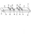
図5は、この発明の実施の形態5に係わる背面光源装置を示す。図5によれば、半導体発光素子列1と、半導体発光素子列3は隣り同士の列である。実施の形態5では、隣接する2つの列中の半導体発光素子において、第1の列中で隣接する半導体発光素子の間に、第2の列中の半導体発光素子が配置されている。例えば、半導体発光素子列1中にある半導体発光素子9は、半導体素子列3中にある隣り同士の半導体発光素子11と12の間に配置される。また、半導体発光素子列1中にある半導体発光素子10は、半導体発光素子列3中にある半導体発光素子12と13の間にあるように配置される。
FIG. 5 shows a back light source device according to Embodiment 5 of the present invention. According to FIG. 5, the semiconductor light emitting element row 1 and the semiconductor light
上記構成では、隣接する2つ列1、3の半導体発光素子から出射された光が、各列に対応する導光板を介して、導光拡散板5へ入力する際、一方の列中の隣接する半導体発光素子から出射される光線の間に、他方の列の半導体発光素子からの光線が位置する。したがって、明るさにむらの少ない背面光源装置を実現できる。 In the above configuration, when the light emitted from the semiconductor light emitting elements in the adjacent two
実施の形態6.
図6は、この発明の実施の形態6に係わる背面光源装置を示す。実施の形態6では、隣接する2つの発光素子の列が設けられ、列1中の隣接する発光素子は、それぞれ第1の原色の光と第2の原色の光を出射し、列1中で隣接する発光素子の間に配置される列3中の発光素子は、第3の原色の光を出射する。例えば、列1では、緑色15、赤色17、青色19の半導体発光素子が順に並ぶ。列3では、赤色14、青色16、緑色18の半導体発光素子が順に並ぶ。例えば、列1中にある緑色15は、列3中にある隣り同士の赤色14と青色16の間に配置される。また、列1中にある赤色17は、列3中にある隣り同士の青色16と緑色18の間に配置される。これらの複数の異なる原色光が合成されて、全体として白色となるように配列されている。
FIG. 6 shows a back light source device according to Embodiment 6 of the present invention. In
上記構成で、2列の半導体発光素子1、3から出射された各原色光が、各列に対応する導光板へ入射し、更に導光拡散板へ入射されて、全体として白色となるので、色のむらの少ない背面光源を実現できる。 With the above configuration, each primary color light emitted from the two rows of semiconductor
実施の形態7.
図7は、この発明の実施の形態7に係わる背面光源装置を示す。導光板2、4と導光拡散板5が、重ねられて配置される。導光板2、4の光出力部と、導光拡散板5の光入力部とに、対向するように、反射鏡20が設けられている。
FIG. 7 shows a back light source device according to
半導体発光素子の列1から出射した光は、導光板2を透過し、反射鏡20により反射されて、導光拡散板5へ入射する。半導体発光素子の列3から出射した光は、導光板4を透過し、反射鏡20により反射されて、導光拡散板5へ入射する。導光拡散板5へ入射した光は、導光拡散板5にて均一に拡散するので、小型で、明るさにむらの無い背面光源装置を実現できる。 The light emitted from the column 1 of the semiconductor light emitting elements is transmitted through the
実施の形態8.
図8は、この発明の実施の形態8に係わる背面光源装置を示す。実施の形態8では、導光拡散板5が、2つの光入力部22、23を有し、導光拡散板5を挟むようにして、光入力部22、23に対向する反射鏡21、20を設ける。反射鏡20、21は円柱状の凹面を有する。
FIG. 8 shows a back light source device according to
半導体発光素子の列1Aから出射した光は、曲面を有する反射フィルム28により反射されて導光板24へ入射し、導光板24を透過し、反射鏡20により反射されて、光入力部22へ入射する。半導体発光素子の列3Aから出射した光は、曲面を有する反射フィルム29により反射されて導光板25へ入射し、導光板25を透過し、反射鏡20により反射されて、光入力部22へ入射する。 The light emitted from the
半導体発光素子の列1Bから出射した光は、曲面を有する反射フィルム31により反射されて導光板27へ入射し、導光板27を透過し、反射鏡21により反射されて、光入力部23へ入射する。半導体発光素子の列3Bから出射した光は、曲面を有する反射フィルム30により反射されて導光板26へ入射し、導光板26を透過し、反射鏡21により反射されて、光入力部23へ入射する。半導体発光素子の列1A、1B、3A、3Bを、図7に示すように、導光板24、25、26、27の光入力部に直接対向するように配置してもよい。複数入力部から導光拡散板5に入射した光が均一に拡散するので、小型で、高輝度のむらの無い背面光源装置を実現できる。 The light emitted from the
以上、実施の形態1から8を説明したが、これらの実施の形態を更に組み合わせて背面光源装置を構成することも可能である。 Although Embodiments 1 to 8 have been described above, it is also possible to configure a back light source device by further combining these embodiments.
1、3 半導体発光素子列、 2、4、6、7、8 導光板、 5 導光拡散板、 9、10、11、12、13、14 導体発光素子、 15、16、17、18、19 半導体発光素子、 20、21 反射鏡、 22、23 光入力部。
1, 3 Semiconductor light emitting element row, 2, 4, 6, 7, 8 Light guide plate, 5 Light guide diffuser plate, 9, 10, 11, 12, 13, 14 Conductor light emitting element, 15, 16, 17, 18, 19 Semiconductor light emitting element, 20, 21 reflector, 22, 23 Light input part.
Claims (3)
Translated fromJapanese複数列の半導体発光素子と、
各々が、前記複数列の半導体発光素子の各列に対応する複数の導光板であり、対応する列の半導体発光素子から出射された光のみを前記導光拡散板へ導く前記複数の導光板とを有し、
前記複数列の半導体発光素子の隣接する2つの列において、第1の列中で隣接する発光素子間に、第2の列中の発光素子が配列されることを特徴とする背面光源装置。In a back light source device that uses a semiconductor light emitting element as a light source and diffuses light emitted from the light source with a single light guide diffusion plate,
A plurality of rows of semiconductor light emitting devices;
Each said a plurality of rows plurality of light guide plates corresponding to each columnof the semiconductor light emitting device, and a correspondingplurality of light guide platesonly light emitted from the semiconductor light emitting element row leading tothe light diffusing plate Have
2. A back light source device according to claim 1, wherein in two adjacent rows of the plurality of rows of semiconductor light emitting devices, the light emitting devices in the second row are arranged between the light emitting devices adjacent in the first row.
前記第2の列は、第1の原色の光を出射する第1の発光素子と、第2の原色の光を出射する第2の発光素子と、第3の原色の光を出射する第3の発光素子とがこの順序で整列する複数の素子列を直列接続してなり、前後に隣接する2つの素子列のうち、後の素子列の第1の発光素子が、前の素子列の第3の発光素子に隣接するように構成され、
前記第1の列中の隣接する2つの発光素子の間に位置する前記第2の列中の発光素子は、前記第1の列中の隣接する2つの発光素子が出射する光とは異なる原色の光を出射することを特徴とする請求項1に記載の背面光源装置。The first row includes a first light emitting element that emits light of a first primary color, a second light emitting element that emits light of a second primary color, and a third light that emits light of a third primary color. A plurality of element rows arranged in this order in series are connected in series, and of the two adjacent element rows, the first light-emitting element in the subsequent element row is the first element row in the previous element row. 3 adjacent to the light emitting element 3
The second row includes a first light emitting element that emits light of a first primary color, a second light emitting element that emits light of a second primary color, and a third light that emits light of a third primary color. A plurality of element rows arranged in this order in series are connected in series, and of the two adjacent element rows, the first light-emitting element in the subsequent element row is the first element row in the previous element row. 3 adjacent to the light emitting element 3
The light emitting elements in the second column located between two adjacent light emitting elements in the first column are different from the light emitted by the two adjacent light emitting elements in the first column. The rear light source device according to claim 1, wherein the rear light source device emits the light of.
Priority Applications (1)
| Application Number | Priority Date | Filing Date | Title |
|---|---|---|---|
| JP2004059047AJP4040027B2 (en) | 2004-03-03 | 2004-03-03 | Rear light source device |
Applications Claiming Priority (1)
| Application Number | Priority Date | Filing Date | Title |
|---|---|---|---|
| JP2004059047AJP4040027B2 (en) | 2004-03-03 | 2004-03-03 | Rear light source device |
Publications (2)
| Publication Number | Publication Date |
|---|---|
| JP2005250020A JP2005250020A (en) | 2005-09-15 |
| JP4040027B2true JP4040027B2 (en) | 2008-01-30 |
Family
ID=35030564
Family Applications (1)
| Application Number | Title | Priority Date | Filing Date |
|---|---|---|---|
| JP2004059047AExpired - Fee RelatedJP4040027B2 (en) | 2004-03-03 | 2004-03-03 | Rear light source device |
Country Status (1)
| Country | Link |
|---|---|
| JP (1) | JP4040027B2 (en) |
Cited By (3)
| Publication number | Priority date | Publication date | Assignee | Title |
|---|---|---|---|---|
| CN103244846A (en)* | 2012-02-03 | 2013-08-14 | 中强光电股份有限公司 | Light source module |
| US8998474B2 (en) | 2011-01-21 | 2015-04-07 | Mitsubishi Electric Corporation | Surface light source device and liquid crystal display apparatus |
| US9103950B2 (en) | 2011-02-15 | 2015-08-11 | Mitsubishi Electric Corporation | Surface light source device and liquid crystal display device |
Families Citing this family (2)
| Publication number | Priority date | Publication date | Assignee | Title |
|---|---|---|---|---|
| WO2007122758A1 (en)* | 2006-04-19 | 2007-11-01 | Sharp Kabushiki Kaisha | Backlight device and display using it |
| WO2008149566A1 (en)* | 2007-06-06 | 2008-12-11 | Sharp Kabushiki Kaisha | Backlight unit and liquid crystal display |
- 2004
- 2004-03-03JPJP2004059047Apatent/JP4040027B2/ennot_activeExpired - Fee Related
Cited By (4)
| Publication number | Priority date | Publication date | Assignee | Title |
|---|---|---|---|---|
| US8998474B2 (en) | 2011-01-21 | 2015-04-07 | Mitsubishi Electric Corporation | Surface light source device and liquid crystal display apparatus |
| US9103950B2 (en) | 2011-02-15 | 2015-08-11 | Mitsubishi Electric Corporation | Surface light source device and liquid crystal display device |
| CN103244846A (en)* | 2012-02-03 | 2013-08-14 | 中强光电股份有限公司 | Light source module |
| US9075175B2 (en) | 2012-02-03 | 2015-07-07 | Coretronic Corporation | Light source module |
Also Published As
| Publication number | Publication date |
|---|---|
| JP2005250020A (en) | 2005-09-15 |
Similar Documents
| Publication | Publication Date | Title |
|---|---|---|
| US6007209A (en) | Light source for backlighting | |
| JP4529573B2 (en) | Planar light source device and liquid crystal display device | |
| KR100771324B1 (en) | Surface illuminator and liquid crystal display having the same | |
| US7097317B2 (en) | Liquid crystal display module | |
| JP2004311353A (en) | Planar light source device and liquid crystal display device using the same | |
| US7585098B2 (en) | Light source device and liquid crystal display device using the same | |
| JP2004342587A (en) | Backlight and liquid crystal display device using the same | |
| CN101089704B (en) | Light source apparatus and display apparatus | |
| JP2006156039A (en) | Planar light source device and liquid crystal display device using the same | |
| JP2006024439A (en) | Surface light source device | |
| JP4338540B2 (en) | Planar light source device and display device using the same | |
| US20080204631A1 (en) | Surface light source device and display | |
| JP2004199967A (en) | Planar light source device, liquid crystal display device, and display device | |
| JP4604801B2 (en) | Planar light source device and display device using the same | |
| JP2001184924A (en) | Plane light source apparatus | |
| JP2008210527A (en) | Light guide plate, surface light source, and liquid crystal display device | |
| JP2005100837A (en) | Surface light source device and display device | |
| JP2005183124A (en) | Planar light source and liquid crystal display device | |
| JP2009026635A (en) | Illumination device and liquid crystal display device | |
| US20070146573A1 (en) | Light emitting diode backlight module and liquid crystal display | |
| JP2006066328A (en) | Light source module and planar lighting device using the light source module | |
| JP4040027B2 (en) | Rear light source device | |
| JP2001101916A (en) | Surface light source device | |
| JP2008293826A (en) | Planar light source device and display device | |
| JP4096540B2 (en) | Surface light source |
Legal Events
| Date | Code | Title | Description |
|---|---|---|---|
| A977 | Report on retrieval | Free format text:JAPANESE INTERMEDIATE CODE: A971007 Effective date:20060915 | |
| A131 | Notification of reasons for refusal | Free format text:JAPANESE INTERMEDIATE CODE: A131 Effective date:20060926 | |
| A521 | Request for written amendment filed | Free format text:JAPANESE INTERMEDIATE CODE: A523 Effective date:20061124 | |
| A131 | Notification of reasons for refusal | Free format text:JAPANESE INTERMEDIATE CODE: A131 Effective date:20070724 | |
| A521 | Request for written amendment filed | Free format text:JAPANESE INTERMEDIATE CODE: A523 Effective date:20070925 | |
| TRDD | Decision of grant or rejection written | ||
| A01 | Written decision to grant a patent or to grant a registration (utility model) | Free format text:JAPANESE INTERMEDIATE CODE: A01 Effective date:20071106 | |
| A61 | First payment of annual fees (during grant procedure) | Free format text:JAPANESE INTERMEDIATE CODE: A61 Effective date:20071106 | |
| FPAY | Renewal fee payment (event date is renewal date of database) | Free format text:PAYMENT UNTIL: 20101116 Year of fee payment:3 | |
| R150 | Certificate of patent or registration of utility model | Ref document number:4040027 Country of ref document:JP Free format text:JAPANESE INTERMEDIATE CODE: R150 Free format text:JAPANESE INTERMEDIATE CODE: R150 | |
| FPAY | Renewal fee payment (event date is renewal date of database) | Free format text:PAYMENT UNTIL: 20111116 Year of fee payment:4 | |
| FPAY | Renewal fee payment (event date is renewal date of database) | Free format text:PAYMENT UNTIL: 20121116 Year of fee payment:5 | |
| FPAY | Renewal fee payment (event date is renewal date of database) | Free format text:PAYMENT UNTIL: 20121116 Year of fee payment:5 | |
| FPAY | Renewal fee payment (event date is renewal date of database) | Free format text:PAYMENT UNTIL: 20131116 Year of fee payment:6 | |
| R250 | Receipt of annual fees | Free format text:JAPANESE INTERMEDIATE CODE: R250 | |
| R250 | Receipt of annual fees | Free format text:JAPANESE INTERMEDIATE CODE: R250 | |
| R250 | Receipt of annual fees | Free format text:JAPANESE INTERMEDIATE CODE: R250 | |
| R250 | Receipt of annual fees | Free format text:JAPANESE INTERMEDIATE CODE: R250 | |
| R250 | Receipt of annual fees | Free format text:JAPANESE INTERMEDIATE CODE: R250 | |
| R250 | Receipt of annual fees | Free format text:JAPANESE INTERMEDIATE CODE: R250 | |
| LAPS | Cancellation because of no payment of annual fees |