JP4032216B2 - OPTICAL MULTILAYER STRUCTURE, ITS MANUFACTURING METHOD, OPTICAL SWITCHING DEVICE, AND IMAGE DISPLAY DEVICE - Google Patents
OPTICAL MULTILAYER STRUCTURE, ITS MANUFACTURING METHOD, OPTICAL SWITCHING DEVICE, AND IMAGE DISPLAY DEVICEDownload PDFInfo
- Publication number
- JP4032216B2 JP4032216B2JP2001212251AJP2001212251AJP4032216B2JP 4032216 B2JP4032216 B2JP 4032216B2JP 2001212251 AJP2001212251 AJP 2001212251AJP 2001212251 AJP2001212251 AJP 2001212251AJP 4032216 B2JP4032216 B2JP 4032216B2
- Authority
- JP
- Japan
- Prior art keywords
- layer
- optical
- refractive index
- multilayer structure
- substrate
- Prior art date
- Legal status (The legal status is an assumption and is not a legal conclusion. Google has not performed a legal analysis and makes no representation as to the accuracy of the status listed.)
- Expired - Fee Related
Links
- 230000003287optical effectEffects0.000titleclaimsdescription183
- 238000004519manufacturing processMethods0.000titleclaimsdescription15
- 239000000758substrateSubstances0.000claimsdescription67
- 239000010408filmSubstances0.000claimsdescription57
- 239000000463materialSubstances0.000claimsdescription39
- 238000000034methodMethods0.000claimsdescription20
- 230000008033biological extinctionEffects0.000claimsdescription15
- 238000013461designMethods0.000claimsdescription8
- 238000005530etchingMethods0.000claimsdescription8
- 239000012788optical filmSubstances0.000claimsdescription8
- BLIQUJLAJXRXSG-UHFFFAOYSA-N1-benzyl-3-(trifluoromethyl)pyrrolidin-1-ium-3-carboxylateChemical compoundC1C(C(=O)O)(C(F)(F)F)CCN1CC1=CC=CC=C1BLIQUJLAJXRXSG-UHFFFAOYSA-N0.000claimsdescription6
- XUIMIQQOPSSXEZ-UHFFFAOYSA-NSiliconChemical compound[Si]XUIMIQQOPSSXEZ-UHFFFAOYSA-N0.000claimsdescription6
- 238000010521absorption reactionMethods0.000claimsdescription6
- 239000002131composite materialSubstances0.000claimsdescription6
- 150000004767nitridesChemical class0.000claimsdescription6
- 229910052710siliconInorganic materials0.000claimsdescription6
- 239000010703siliconSubstances0.000claimsdescription6
- NRTOMJZYCJJWKI-UHFFFAOYSA-NTitanium nitrideChemical compound[Ti]#NNRTOMJZYCJJWKI-UHFFFAOYSA-N0.000claimsdescription5
- -1hafnium nitrideChemical class0.000claimsdescription5
- 230000008859changeEffects0.000claimsdescription4
- 230000001678irradiating effectEffects0.000claimsdescription4
- MZLGASXMSKOWSE-UHFFFAOYSA-Ntantalum nitrideChemical compound[Ta]#NMZLGASXMSKOWSE-UHFFFAOYSA-N0.000claimsdescription4
- 239000012780transparent materialSubstances0.000claimsdescription4
- 229910052735hafniumInorganic materials0.000claimsdescription3
- ZVWKZXLXHLZXLS-UHFFFAOYSA-Nzirconium nitrideChemical compound[Zr]#NZVWKZXLXHLZXLS-UHFFFAOYSA-N0.000claimsdescription3
- 230000031700light absorptionEffects0.000claims3
- 229910006404SnO 2Inorganic materials0.000claims1
- 239000010410layerSubstances0.000description109
- 238000010586diagramMethods0.000description12
- 230000005611electricityEffects0.000description7
- 239000011521glassSubstances0.000description7
- 230000003068static effectEffects0.000description7
- 239000010409thin filmSubstances0.000description7
- 229910021417amorphous siliconInorganic materials0.000description6
- 229910052581Si3N4Inorganic materials0.000description5
- 230000005540biological transmissionEffects0.000description5
- 238000001312dry etchingMethods0.000description5
- HQVNEWCFYHHQES-UHFFFAOYSA-Nsilicon nitrideChemical compoundN12[Si]34N5[Si]62N3[Si]51N64HQVNEWCFYHHQES-UHFFFAOYSA-N0.000description5
- 230000004048modificationEffects0.000description4
- 238000012986modificationMethods0.000description4
- 230000004044responseEffects0.000description4
- 238000001039wet etchingMethods0.000description4
- OKTJSMMVPCPJKN-UHFFFAOYSA-NCarbonChemical compound[C]OKTJSMMVPCPJKN-UHFFFAOYSA-N0.000description3
- 238000003491arrayMethods0.000description3
- 238000005229chemical vapour depositionMethods0.000description3
- 239000003086colorantSubstances0.000description3
- 229920002120photoresistant polymerPolymers0.000description3
- 230000010287polarizationEffects0.000description3
- XOLBLPGZBRYERU-UHFFFAOYSA-Ntin dioxideChemical compoundO=[Sn]=OXOLBLPGZBRYERU-UHFFFAOYSA-N0.000description3
- LFQSCWFLJHTTHZ-UHFFFAOYSA-NEthanolChemical compoundCCOLFQSCWFLJHTTHZ-UHFFFAOYSA-N0.000description2
- PEDCQBHIVMGVHV-UHFFFAOYSA-NGlycerineChemical compoundOCC(O)COPEDCQBHIVMGVHV-UHFFFAOYSA-N0.000description2
- 229910010421TiNxInorganic materials0.000description2
- WGLPBDUCMAPZCE-UHFFFAOYSA-NTrioxochromiumChemical compoundO=[Cr](=O)=OWGLPBDUCMAPZCE-UHFFFAOYSA-N0.000description2
- 229910000423chromium oxideInorganic materials0.000description2
- 238000004891communicationMethods0.000description2
- 239000000470constituentSubstances0.000description2
- 239000007789gasSubstances0.000description2
- 229910002804graphiteInorganic materials0.000description2
- 239000010439graphiteSubstances0.000description2
- AMGQUBHHOARCQH-UHFFFAOYSA-Nindium;oxotinChemical compound[In].[Sn]=OAMGQUBHHOARCQH-UHFFFAOYSA-N0.000description2
- 239000004973liquid crystal related substanceSubstances0.000description2
- 229910052751metalInorganic materials0.000description2
- 239000002184metalSubstances0.000description2
- 238000001020plasma etchingMethods0.000description2
- 239000002356single layerSubstances0.000description2
- 229910052715tantalumInorganic materials0.000description2
- GUVRBAGPIYLISA-UHFFFAOYSA-Ntantalum atomChemical compound[Ta]GUVRBAGPIYLISA-UHFFFAOYSA-N0.000description2
- NAWXUBYGYWOOIX-SFHVURJKSA-N(2s)-2-[[4-[2-(2,4-diaminoquinazolin-6-yl)ethyl]benzoyl]amino]-4-methylidenepentanedioic acidChemical compoundC1=CC2=NC(N)=NC(N)=C2C=C1CCC1=CC=C(C(=O)N[C@@H](CC(=C)C(O)=O)C(O)=O)C=C1NAWXUBYGYWOOIX-SFHVURJKSA-N0.000description1
- IJGRMHOSHXDMSA-UHFFFAOYSA-NAtomic nitrogenChemical compoundN#NIJGRMHOSHXDMSA-UHFFFAOYSA-N0.000description1
- DGAQECJNVWCQMB-PUAWFVPOSA-MIlexoside XXIXChemical compoundC[C@@H]1CC[C@@]2(CC[C@@]3(C(=CC[C@H]4[C@]3(CC[C@@H]5[C@@]4(CC[C@@H](C5(C)C)OS(=O)(=O)[O-])C)C)[C@@H]2[C@]1(C)O)C)C(=O)O[C@H]6[C@@H]([C@H]([C@@H]([C@H](O6)CO)O)O)O.[Na+]DGAQECJNVWCQMB-PUAWFVPOSA-M0.000description1
- VYPSYNLAJGMNEJ-UHFFFAOYSA-NSilicium dioxideChemical compoundO=[Si]=OVYPSYNLAJGMNEJ-UHFFFAOYSA-N0.000description1
- GWEVSGVZZGPLCZ-UHFFFAOYSA-NTitan oxideChemical compoundO=[Ti]=OGWEVSGVZZGPLCZ-UHFFFAOYSA-N0.000description1
- XLOMVQKBTHCTTD-UHFFFAOYSA-NZinc monoxideChemical compound[Zn]=OXLOMVQKBTHCTTD-UHFFFAOYSA-N0.000description1
- 239000011358absorbing materialSubstances0.000description1
- 229910052782aluminiumInorganic materials0.000description1
- XAGFODPZIPBFFR-UHFFFAOYSA-NaluminiumChemical compound[Al]XAGFODPZIPBFFR-UHFFFAOYSA-N0.000description1
- 230000015572biosynthetic processEffects0.000description1
- 229910052799carbonInorganic materials0.000description1
- 229910017052cobaltInorganic materials0.000description1
- 239000010941cobaltSubstances0.000description1
- GUTLYIVDDKVIGB-UHFFFAOYSA-Ncobalt atomChemical compound[Co]GUTLYIVDDKVIGB-UHFFFAOYSA-N0.000description1
- 238000011161developmentMethods0.000description1
- 238000001035dryingMethods0.000description1
- 230000000694effectsEffects0.000description1
- 235000019441ethanolNutrition0.000description1
- 230000006870functionEffects0.000description1
- 229910052732germaniumInorganic materials0.000description1
- GNPVGFCGXDBREM-UHFFFAOYSA-Ngermanium atomChemical compound[Ge]GNPVGFCGXDBREM-UHFFFAOYSA-N0.000description1
- 235000011187glycerolNutrition0.000description1
- 239000007788liquidSubstances0.000description1
- 239000000696magnetic materialSubstances0.000description1
- 230000007246mechanismEffects0.000description1
- 239000012528membraneSubstances0.000description1
- 229910044991metal oxideInorganic materials0.000description1
- 150000004706metal oxidesChemical class0.000description1
- 239000010955niobiumSubstances0.000description1
- 229910000484niobium oxideInorganic materials0.000description1
- URLJKFSTXLNXLG-UHFFFAOYSA-Nniobium(5+);oxygen(2-)Chemical compound[O-2].[O-2].[O-2].[O-2].[O-2].[Nb+5].[Nb+5]URLJKFSTXLNXLG-UHFFFAOYSA-N0.000description1
- 229910052755nonmetalInorganic materials0.000description1
- BPUBBGLMJRNUCC-UHFFFAOYSA-Noxygen(2-);tantalum(5+)Chemical compound[O-2].[O-2].[O-2].[O-2].[O-2].[Ta+5].[Ta+5]BPUBBGLMJRNUCC-UHFFFAOYSA-N0.000description1
- 239000004033plasticSubstances0.000description1
- 230000008569processEffects0.000description1
- 239000004065semiconductorSubstances0.000description1
- 229910001285shape-memory alloyInorganic materials0.000description1
- HBMJWWWQQXIZIP-UHFFFAOYSA-Nsilicon carbideChemical compound[Si+]#[C-]HBMJWWWQQXIZIP-UHFFFAOYSA-N0.000description1
- LIVNPJMFVYWSIS-UHFFFAOYSA-Nsilicon monoxideChemical compound[Si-]#[O+]LIVNPJMFVYWSIS-UHFFFAOYSA-N0.000description1
- 229910052814silicon oxideInorganic materials0.000description1
- 229920002545silicone oilPolymers0.000description1
- 229910052708sodiumInorganic materials0.000description1
- 239000011734sodiumSubstances0.000description1
- 238000004544sputter depositionMethods0.000description1
- 238000003860storageMethods0.000description1
- 229910001936tantalum oxideInorganic materials0.000description1
- 229910001887tin oxideInorganic materials0.000description1
- XLYOFNOQVPJJNP-UHFFFAOYSA-NwaterSubstancesOXLYOFNOQVPJJNP-UHFFFAOYSA-N0.000description1
Images


Classifications
- G—PHYSICS
- G02—OPTICS
- G02B—OPTICAL ELEMENTS, SYSTEMS OR APPARATUS
- G02B26/00—Optical devices or arrangements for the control of light using movable or deformable optical elements
- G02B26/08—Optical devices or arrangements for the control of light using movable or deformable optical elements for controlling the direction of light
- G02B26/0816—Optical devices or arrangements for the control of light using movable or deformable optical elements for controlling the direction of light by means of one or more reflecting elements
- G02B26/0833—Optical devices or arrangements for the control of light using movable or deformable optical elements for controlling the direction of light by means of one or more reflecting elements the reflecting element being a micromechanical device, e.g. a MEMS mirror, DMD
- G02B26/0841—Optical devices or arrangements for the control of light using movable or deformable optical elements for controlling the direction of light by means of one or more reflecting elements the reflecting element being a micromechanical device, e.g. a MEMS mirror, DMD the reflecting element being moved or deformed by electrostatic means
- G—PHYSICS
- G02—OPTICS
- G02B—OPTICAL ELEMENTS, SYSTEMS OR APPARATUS
- G02B26/00—Optical devices or arrangements for the control of light using movable or deformable optical elements
- G02B26/001—Optical devices or arrangements for the control of light using movable or deformable optical elements based on interference in an adjustable optical cavity
- G—PHYSICS
- G02—OPTICS
- G02B—OPTICAL ELEMENTS, SYSTEMS OR APPARATUS
- G02B26/00—Optical devices or arrangements for the control of light using movable or deformable optical elements
- G02B26/02—Optical devices or arrangements for the control of light using movable or deformable optical elements for controlling the intensity of light
- G—PHYSICS
- G02—OPTICS
- G02B—OPTICAL ELEMENTS, SYSTEMS OR APPARATUS
- G02B26/00—Optical devices or arrangements for the control of light using movable or deformable optical elements
- G02B26/08—Optical devices or arrangements for the control of light using movable or deformable optical elements for controlling the direction of light
- G02B26/0816—Optical devices or arrangements for the control of light using movable or deformable optical elements for controlling the direction of light by means of one or more reflecting elements
- G02B26/0833—Optical devices or arrangements for the control of light using movable or deformable optical elements for controlling the direction of light by means of one or more reflecting elements the reflecting element being a micromechanical device, e.g. a MEMS mirror, DMD
- G02B26/085—Optical devices or arrangements for the control of light using movable or deformable optical elements for controlling the direction of light by means of one or more reflecting elements the reflecting element being a micromechanical device, e.g. a MEMS mirror, DMD the reflecting means being moved or deformed by electromagnetic means
Landscapes
- Physics & Mathematics (AREA)
- General Physics & Mathematics (AREA)
- Optics & Photonics (AREA)
- Spectroscopy & Molecular Physics (AREA)
- Electromagnetism (AREA)
- Mechanical Light Control Or Optical Switches (AREA)
- Optical Filters (AREA)
- Micromachines (AREA)
Description
Translated fromJapanese【0001】
【発明の属する技術分野】
本発明は、入射光を反射,透過若しくは吸収させる機能を有する光学多層構造体およびその製造方法、並びに光スイッチング素子および画像表示装置に関する。
【0002】
【従来の技術】
近年、映像情報の表示デバイスとしてのディスプレイの重要性が高まっており、このディスプレイ用の素子として、更には、光通信,光記憶装置,光プリンタなどの素子として、高速で動作する光スイッチング素子(ライトバルブ)の開発が要望されている。従来、この種の素子としては、液晶を用いたもの、マイクロミラーを用いたもの(DMD;Digtal Micro Miror Device ,ディジタルマイクロミラーデバイス、テキサスインスツルメンツ社の登録商標)、回折格子を用いたもの(GLV:Grating Light Valve,グレーティングライトバルブ,SLM(シリコンライトマシン)社製)等がある。
【0003】
GLVは回折格子をMEMS(Micro Electro Mechanical Systems) 構造で作製し、静電力で10nsの高速ライトスイッチング素子を実現している。DMDは同じくMEMS構造でミラーを動かすことによりスイッチングを行うものである。これらのデバイスを用いてプロジェクタ等のディスプレイを実現できるものの、液晶とDMDは動作速度が遅いために、ライトバルブとしてディスプレイを実現するためには2次元配列としなければならず、構造が複雑となる。一方、GLVは高速駆動型であるので、1次元アレイを走査することでプロジェクションディスプレイを実現することができる。
【0004】
しかしながら、GLVは回折格子構造であるので、1ピクセルに対して6つの素子を作り込んだり、2方向に出た回折光を何らかの光学系で1つにまとめる必要があるなどの複雑さがある。
【0005】
簡単な構成で実現できるものとしては、米国特許公報5,589,974号や米国特許公報5,500,761号に開示されたものがある。このライトバルブは、基板(屈折率nS)の上に間隙部(ギャップ層)を挟んで、屈折率が√nSの透光性の薄膜を設けた構造を有している。この素子では、静電力を利用して薄膜を駆動し、基板と薄膜との間の距離、すなわち、間隙部の大きさを変化させることにより、光信号を透過あるいは反射させるものである。ここで、薄膜の屈折率は基板の屈折率nSに対して、√nSとなっており、このような関係を満たすことにより、高コントラストの光変調を行うことができるとされている。
【0006】
【発明が解決しようとする課題】
しかしながら、上述のような構成の素子では、基板の屈折率nSが「4」などの大きな値でなければ、可視光領域においては実現することはできないという問題がある。すなわち、透光性薄膜としては、構造体であることを考えると、窒化珪素(Si3N4)(屈折率n=2.0)などの材料が望ましいが、その場合には基板の屈折率nS=4となる。可視光領域では、このような材料の選択肢は狭い。赤外線等の通信用波長では、ゲルマニウム(Ge)(n=4)、シリコン(Si)(n≒4)などを用いることにより実現可能である。
【0007】
また、米国特許公報5,500,761号などで開示されているライトバルブでは、シリコン基板上に間隙部を間にして窒化珪素(Si3N4)などの構造材を配している。しかしながら、この構造では、現在、犠牲層のドライエッチングとして広く認知されている、犠牲層をシリコン(Si)により形成し、これを二フッ化キセノン(XeF2)でエッチングする方法が使えない。なぜなら、基板もSiであるので、犠牲層との選択比が取れないからである。そのために、上記構造では、ウェットエッチングなどの他の方法を用いていると思われる。ウェットエッチングでは、エッチング液がλ/4程度の間隙に入り込んで円滑に循環することが難しく、エッチングできなかったり、また、液の表面張力などで乾燥時に犠牲層の上の構造材が壊れたりして、所望の構造体を作製するのは難しい。なお、光スイッチとなる部品の相対面積を小さくして開口度を小さくすれば、ウェットエッチングなどのプロセスでも実現可能であるが、画像表示用としては、開口度を上げる傾向にあるので、エッチング液が入り込むための部分を少なくしたい。そのために、ウェットエッチングよりはドライエッチングが適している。しかしながら、上述のように基板がSiにより形成されている場合には、犠牲層をSiにより形成し、これをXeF2でエッチングする方法は適用できないという問題がある。
【0008】
本発明はかかる問題点に鑑みてなされたもので、その第1の目的は、簡単な構成で、小型軽量であると共に、構成材料の選択にも自由度があり、かつ可視光領域においても高速応答が可能であり、画像表示装置等に好適に用いることができる光学多層構造体を提供することにある。
【0009】
本発明の第2の目的は、間隙部の形成工程において、犠牲層をSiで形成すると共に、XeF2を用いたドライエッチングを適用でき、開口度の高い光学多層構造体を容易に作製することができる光学多層構造体の製造方法を提供することにある。
【0010】
更に、本発明の第3の目的は、上記光学多層構造体を用いて高速応答が可能な光スイッチング素子および画像表示装置を提供することにある。
【0011】
【課題を解決するための手段】
本発明による第1の光学多層構造体は、基板上に、光の吸収のある第1の層、光の干渉現象を起こし得る大きさを有すると共にその大きさが、λ/4(λは入射光の波長)の奇数倍とλ/4の偶数倍(0を含む)との間で可変な間隙部、および透明な第2の層をこの順で配設した構造を備え、第1の層を、数(9)を満たすN1(=n1−i・k1,n1は屈折率,k1は消衰係数,iは虚数単位)の複素屈折率を有する材料により前記基板の光学的情報が見えなくなる程度に厚く形成すると共に、
前記第2の層を、数(9)を満たすn2の屈折率を有する材料により形成したものである。
【数9】
【0012】
本発明による第2の光学多層構造体は、光の吸収のある基板上に、光の干渉現象を起こし得る大きさを有すると共にその大きさが、λ/4(λは入射光の波長)の奇数倍とλ/4の偶数倍(0を含む)との間で可変な間隙部、および透明層をこの順で配設した構造を備えた光学多層構造体であって、基板を、数(9)を満たすN1(=n1−i・k1,n1は屈折率,k1は消衰係数,iは虚数単位)の複素屈折率を有する材料により形成すると共に、透明層を、数(9)を満たすn2の屈折率を有する材料により形成したものである。
【0013】
本発明による第1の光スイッチング素子は、本発明の第1の光学多層構造体と、この光学多層構造体における間隙部の光学的な大きさを変化させるための駆動手段とを備えたものである。
【0014】
本発明による第2の光スイッチング素子は、本発明の第2の光学多層構造体と、この光学多層構造体における間隙部の光学的な大きさを変化させるための駆動手段とを備えたものである。
【0015】
本発明による第1の画像表示装置は、本発明による第1の光スイッチング素子を複数個、1次元あるいは2次元に配列したものであり、3原色の光を照射し、スキャナによって走査することで2次元画像を表示するものである。
【0016】
本発明による第2の画像表示装置は、本発明による第2の光スイッチング素子を複数個、1次元あるいは2次元に配列したものであり、3原色の光を照射し、スキャナによって走査することで2次元画像を表示するものである。
【0017】
本発明による第1また第2の光学多層構造体では、間隙部の大きさを、「λ/4」(λは入射光の設計波長)の奇数倍と「λ/4」の偶数倍(0を含む)との間で、2値的あるいは連続的に変化させると、入射光の反射、透過若しくは吸収の量が2値的あるいは連続的に変化する。
【0018】
本発明による第1また第2の光スイッチング素子では、駆動手段によって、光学多層構造体の間隙部の光学的な大きさが変化することにより、入射光に対してスイッチング動作がなされる。
【0019】
本発明による第1また第2の画像表示装置では、1次元あるいは2次元に配列された本発明の複数の光スイッチング素子に対して光が照射されることによって2次元画像が表示される。
【0020】
【発明の実施の形態】
以下、本発明の実施の形態について図面を参照して詳細に説明する。
【0021】
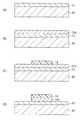
図1および図2は、本発明の一実施の形態に係る光学多層構造体1の基本的な構成を表すものである。図1は光学多層構造体1における後述の間隙部12が存在し、高反射時の状態、図2は光学多層構造体1の間隙部12がなく、低反射時の状態をそれぞれ示している。なお、この光学多層構造体1は具体的には例えば光スイッチング素子として用いられ,この光スイッチング素子を複数個1次元または2次元に配列することにより、画像表示装置を構成することができる。また、詳細は後述するが、図2のような構造に固定した場合には、反射防止膜として利用することができるものである。
【0022】
この光学多層構造体1は、基板10の上に、この基板10に接する、光の吸収のある第1の層11、光の干渉現象を起こし得る大きさを有すると共にその大きさを変化させることのできる間隙部12、および透明の第2の層13をこの順で配設して構成したものである。
【0023】
ここで、本実施の形態では、第1の層11の複素屈折率をN1(=n1−i・k1,n1は屈折率,k1は消衰係数,iは虚数単位)、第2の層13の屈折率をn2、入射媒質の屈折率を1.0としたとき、次式(10)の関係を満たすように設定されている。なお、この式の意義については後述する。
【0024】
【数10】
基板10は、カーボン(C),グラファイト(黒鉛)などの非金属,タンタル(Ta)などの金属,酸化クロム(CrO)などの酸化金属,窒化チタン(TiNX)などの窒化金属,シリコンカーバイド(SiC)などの炭化物,シリコン(Si)などの半導体等の、不透明で光の吸収のある材料により形成されたもの、あるいは、これら光の吸収のある材料の薄膜を透明基板上に成膜したものとしてもよい。基板10は、また、例えばガラス,プラスチックなどの透明材料若しくは消衰係数kの値の低い半透明材料により形成されたものとしてもよい。
【0026】
第1の層11は、光の吸収のある層であり、窒化物材料、例えば窒化チタン(TiNX),窒化タンタル(TaNX),窒化ハフニウム(HfNX)または窒化ジルコニウム(ZrNX)などにより形成されたものである。
【0027】
第2の層13は、透明材料により形成されたものであり、例えば、酸化チタン(TiO2)(n2=2.4),窒化珪素(Si3N4)(n2=2.0),酸化亜鉛(ZnO)(n2=2.0),酸化ニオブ(Nb2O5)(n2=2.2),酸化タンタル(Ta2O5)(n2=2.1),酸化珪素(SiO)(n2=2.0),酸化スズ(SnO2)(n2=2.0),ITO(Indium-Tin Oxide) (n2=2.0)などにより形成されている。
【0028】
なお、この第2の層13は、スイッチング動作時においては、後述のように可動部として作用するため、特に、ヤング率が高く、丈夫なSi3N4などで形成されたものであることが好ましい。また、静電気により駆動する場合には、第2の層13の一部にITOなどの透明導電膜を含めるようにすればよい。Si3N4とITOの屈折率は同等であるので、それぞれどの程度の膜厚にするかは任意である。また、第1の層11と第2の層13とが接触する場合には、接触時に電気的に短絡しないように、第2の層13の基板側をSi3N4、入射媒質側をITOとすることが望ましい。
【0029】
第1の層11の物理的な膜厚d1は、入射光の波長、その材料のnとkの値により決まるが、本実施の形態では、基板10の光学的情報が見えなくなる程度に十分厚くする。その理由および各材料の具体的な膜厚については後述する。
【0030】
第2の層13の光学的な膜厚n2・d2は、「λ/4」(λは入射光の設計波長)以下である。
【0031】
なお、本明細書中の表記での「λ/4」は厳密に「λ/4」でなくとも、これらの近傍の値でもよい。これは、例えば、一方の層の光学膜厚がλ/4より厚くなった分、他方の層を薄くするなどして補完できるからであり、また、上式(8)から屈折率が多少ずれた場合でも、膜厚で調整可能な場合もあるからである。よって、本明細書においては、「λ/4」の表現には「ほぼλ/4」の場合も含まれるものとする。
【0032】
なお、第1の層11および第2の層13は、互いに光学的特性の異なる2以上の層で構成された複合層としてもよいが、この場合には複合層における合成した光学的特性(光学アドミッタンス)が単層の場合と同等な特性を有するものとする必要がある。
【0033】
間隙部12は、後述の駆動手段によって、その光学的な大きさ(第1の層11と第2の層13との間隔)が可変であるように設定されている。間隙部12を埋める媒体は、透明であれば気体でも液体でもよい。気体としては、例えば、空気(ナトリウムD線(589.3nm)に対する屈折率nD=1.0)、窒素(N2)(nD=1.0)など、液体としては、水(nD=1.333)、シリコーンオイル(nD=1.4〜1.7)、エチルアルコール(nD=1.3618)、グリセリン(nD=1.4730)、ジョードメタン(nD=1.737)などが挙げられる。なお、間隙部12を真空状態とすることもできる。
【0034】
間隙部12の光学的な大きさは、「λ/4の奇数倍」と「λ/4の偶数倍(0を含む)」との間で、2値的あるいは連続的に変化するものである。これにより入射光の反射、透過若しくは吸収の量が2値的あるいは連続的に変化する。なお、上記第1の層11および第2の層13の膜厚の場合と同様に、λ/4の倍数から多少ずれても、他の層の膜厚あるいは屈折率の多少の変化で補完できるので、「λ/4」の表現には、「ほぼλ/4」の場合も含まれるものとする。
【0035】
このような間隙部12を有する光学多層構造体1は、図3および図4に示した製造プロセスにより作製することができる。まず、図3(A)に示したように例えばガラスからなる基板10の上に、例えばスパッタリング法によりTaNXからなる第1の層11を形成し、次いで,図3(B)に示したように例えばCVD(Chemical Vapor Deposition:化学的気相成長 )法により犠牲層としての非晶質シリコン(a−Si)膜12aを形成する。続いて、図3(C)に示したように、間隙部12のパターン形状を有するフォトレジスト膜14を形成し、図3(D)に示したようにこのフォトレジスト膜14をマスクとして、例えばRIE(Reactive Ion Etching) により非晶質シリコン(a−Si)膜12aを選択的に除去する。
【0036】
次に、図4(A)に示したようにフォトレジスト膜14を除去した後、図4(B)に示したように例えばCVD法によりSi3N4からなる第2の層13を形成する。次いで、図4(C)に示したように、二フッ化キセノン(XeF2)などのドライエッチングにより非晶質シリコン(a−Si)膜12aを除去する。これにより、間隙部12を備えた光学多層構造体1を作製することができる。
【0037】
本実施の形態の光学多層構造体1は、間隙部12の光学的な大きさを、λ/4の奇数倍とλ/4の偶数倍(0を含む)との間(例えば、「λ/4」と「0」との間)で、2値的あるいは連続的に変化させることによって、入射した光の反射,透過若しくは吸収の量を変化させるものである。
【0038】
次に、図1および図5を参照して、上記式(5)の意義について説明する。
【0039】
上記のような光学多層構造体1のフィルタ特性は、光学アドミッタンスによって説明することができる。光学アドミッタンスyは、複素屈折率N(=n−i・k、nは屈折率,kは消衰係数,iは虚数単位)と値が同じである。例えば、空気のアドミッタンスはy(air) =1 、n(air) =1 、ガラスのアドミッタンスはy(glass) =1.52、n(glass) =1.52である。
【0040】
光学アドミッタンスダイアグラム上で、n2の屈折率を持つ透明な第2の層が、ダイアグラム上の(1,0)の点 (空気のアドミッタンス) を通る軌跡を描くと、図5のようになる。すなわち、実軸Re(Y)上で1とn22を通り、中心が(n22+1)/2の円弧となる。ここで、基板10上に、基板10の光学的情報が見えなくなるくらい十分厚く第1の層11を成膜した場合、第1の層11が光学上は基板10と同等の役割を担う。その第1の層11の材料の光学アドミッタンス (=複素屈折率(n1−i・k1))が、ほぼこの円弧の上にある場合、その点から第1の層11と第2の層13の合成アドミッタンスが移動する。そして、合成アドミッタンスが1となるような膜厚で第2の層13を成膜する。このようにすれば、反射は、設計波長において0となる。かかる条件を満たすための、基板10または第1の層11の材料と第2の層13の材料の光学定数の関係は、前述の式(10)のようになる。但し、別の光学定数を持った材料をごく薄く配することで合成アドミッタンスが1に帰着することもあるので、式(10)を完全に満たさなくても良い場合もあることから、式(10)をほぼ満たす状態であればよい。
【0041】
すなわち、この光学多層構造体1では、第1の層11と第2の層13との間の間隙部12の間隔が「0」のときには反射防止膜となり、その間隔が設計波長に対し光学的にほぼλ/4の時には反射膜となる。つまり、間隔を「0」と「λ/4」との間で可変とすることで、後述のように反射率を「0」と「70%」以上とに変えられる光スイッチング素子を実現することができる。
【0042】
なお、基板10そのものが上記第1の層の複素屈折率を持てば、図6に示したように第1の層の無い、光学多層構造体2とすることができる。この光学多層構造体2では、基板10Aの複素屈折率をN1(=n1−i・k1,n1は屈折率,k1は消衰係数,iは虚数単位)、透明層13A(第2の層13に相当)の屈折率をn2、入射媒質の屈折率を1.0としたときに、上式(10)の関係を満たすように設定すればよい。
【0043】
このような光学多層構造体の材料の組み合わせとしては、上記のような制約を満足すればよく、その選定の自由度は広い。表1はその一例を表すものである。なお、窒化タンタルとITOは本発明者が実際に成膜した実測値であり、Si3N4は一般的な値である。
【0044】
【表1】
ここでは、第1の層11としてTaNX層、間隙部12として空気層(n=1.00)、第2の層13としてSi3N4膜とITO膜との積層膜(合成屈折率n2=2.0,k=0)を用いた。TaNX層は400nmと厚くした。設計波長550nmで、その波長において第1の層11のTaNXの光学特性は前述の式(10)をほぼ満たす。第2の層13の膜厚は、Si3N4とITOの屈折率はほぼ2.0で同等であるので、合計で60nmあればよい。ここでは、上層のITOを20nm、下層のSi3N4を40nmとした。
【0046】
図7は、このような構成で、入射光の波長(設計波長550nm)と反射率との関係をシミュレーションした結果を表すものである。ここで、Aは間隙部(空気層)の光学膜厚が「0」(低反射側)、Bは光学膜厚が「λ/4」(138nm)(高反射側)の場合の特性をそれぞれ表している。また、図8は、低反射時の合成光学アドミッタンスダイヤグラムを示すもので、合成光学アドミッタンスが1.0近傍に終着していることが分かる。このような条件を満足する第1の層11の材料としては前述のように窒化物が好ましい。そのうち窒化タンタルは表1に示したとおりである。なお、窒化物は成膜条件によりnとkの値をある程度調整することが可能であり、窒化チタン(TiNX),窒化ハフニウム(HfNX)または窒化ジルコニウム(ZrNX)などは条件を満足する。表2は、一例として、HfN,TaNX,TiNについて、各波長に対するn,kと、基板10の光学的情報が見えなくなる程度の十分な厚さの値の目安を示したものである。
【0047】
【表2】
このように本実施の形態では、例えば550nmなどの可視光領域においても、低反射時の反射率を殆ど0、高反射時の反射率を70%以上とすることができるので、高コントラストな変調を行うことが可能である。しかも、構成が簡単であるので、GLVなどの回折格子構造やDMDなどの複雑な3次元構造よりも容易に作製することができる。また、GLVは1つのピクセルに6本の格子状のリボンが必要であるが、本実施の形態では1本で済むので、構成が簡単であり、かつ小さく作製することが可能である。また、可動部分の移動範囲も高々「λ/2」であるため、10nsレベルの高速応答が可能になる。よって、ディスプレイ用途のライトバルブとして用いる場合には、後述のように1次元アレイの簡単な構成で実現することができる。
【0049】
更に、本実施の形態の光学多層構造体1は、間隙部を金属薄膜や反射層で挟んだ構造の狭帯域透過フィルタ、すなわちファブリーペロータイプのものとは本質的に異なるものであるため、低反射帯の帯域幅を広くすることができる。よって、製作時の膜厚管理のマージンを比較的広くとることが可能であり、設計の自由度が増す。
【0050】
また、本実施の形態では、基板10および第1の層11の屈折率はある範囲の任意の値であれば良いため、材料の選択の自由度が広くなる。なお、基板10を不透明な材料により構成した場合には、低反射時において入射光は基板10に吸収されるので、迷光などが発生する心配はなくなる。
【0051】
なお、本出願人と同一出願人は、先に、基板上に、光の吸収のある第1の層、光の干渉現象を起こし得る大きさを有すると共にその大きさが可変な間隙部、および第2の層を配設した構造を有する光学多層構造体を提案した(特願2000−219599)。この光学多層構造体は、簡単な構成で、構成材料の選択にも自由度があり、かつ可視光領域においても高速応答が可能であり、画像表示装置等に好適に用いることができる。しかし、この光学多層構造体を実現するには、第1の層(導電層)の膜厚が限定され、しかも、その膜厚は10nm前後と薄くなる。導電層がこの程度の膜厚であると、ときによっては電気抵抗が大きくなる。これに対して、本実施の形態では、第1の層(導電層)の膜厚を、基板の光学的情報が見えなくなるほどに十分に厚くするため、その電気抵抗が小さくなり、配線としての信頼性が向上する。
【0052】
以上のように、本実施の形態の光学多層構造体1を用いることにより、高速で小型であり、しかも信頼性の向上した光スイッチング素子および画像表示装置を実現することができる。これらの詳細については後述する。
【0053】
なお、上記実施の形態では、光学多層構造体1の間隙部を一層としたが、複数層、例えば図9に示したように2層設けるようにしてもよい。これは、基板10上に、第1の層11、第1の間隙部12、第2の層13、第2の間隙部30、第3の透明層31をこの順に形成し、第2の層13および第3の透明層31をそれぞれ例えば窒化シリコンからなる支持体15,32により支持する構成としたものである。
【0054】
この光学多層構造体では、中間の第2の層13が上下に変位し、第1の間隙部12と第2の間隙部30の一方の間隙が狭くなった分、他方の間隙部が広まることにより反射特性が変化する。
【0055】
〔駆動方法〕
次に、上記光学多層構造体1における間隙部12の大きさを変化させるための具体的な手段について説明する。
【0056】
図10は、静電気により光学多層構造体を駆動する例を示している。この光学多層構造体は、透明基板10の上の第1の層11の両側にそれぞれ例えばアルミニウムからなる電極16a,16aを設けると共に、第2の層13を例えば窒化シリコン(Si3N4)からなる支持体15により支持し、この支持体15の電極16a,16aに対向する位置に電極16b,16bを形成したものである。
【0057】
この光学多層構造体では、電極16a,16aおよび電極16b,16bへの電圧印加による電位差で生じた静電引力によって、間隙部12の光学膜厚を、例えば「λ/4」と、「0」との間、あるいは「λ/4」と「λ/2」との間で2値的に切り替える。勿論、電極16a,16a、電極16b,16bへの電圧印加を連続的に変化させることにより、間隙部12の大きさをある値の範囲で連続的に変化させ、入射した光の反射、若しくは透過あるいは吸収等の量を連続的(アナログ的)に変化させるようにすることもできる。
【0058】
光学多層構造体を静電気で駆動するものとしては、その他、図11および図12に示した方法によってもよい。図11に示した光学多層構造体1は、透明基板10の上の第1の層11上に例えばITO(Indium-Tin Oxide) からなる透明導電膜17aを設けると共に、例えばSiO2からなる第2の層13を架橋構造に形成し、この第2の層13の外面に同じくITOからなる透明導電膜17bを設けたものである。
【0059】
この光学多層構造体では、透明導電膜17a,17b間への電圧印加による電位差で生じた静電引力によって、間隙部12の光学膜厚を切り替えることができる。
【0060】
図12に示した光学多層構造体では、図11の光学多層構造体の透明導電膜17aの代わりに、導電性のある第1の層11として例えばタンタル(Ta)膜を配したものである。
【0061】
光学多層構造体の駆動は、このような静電気の他、トグル機構や圧電素子などのマイクロマシンを用いる方法、磁力を用いる方法や、形状記憶合金を用いる方法など、種々考えられる。図13(A),(B)は磁力を用いて駆動する態様を示したものである。この光学多層構造体では、第2の層13の上に開孔部を有するコバルト(Co)などの磁性材料からなる磁性層40を設けると共に基板10の下部に電磁コイル41を設けたものであり、この電磁コイル41のオン・オフの切り替えにより、間隙部12の間隔を例えば「λ/4」(図13(A))と「0」(図13(B))との間で切り替え、これにより反射率を変化させることができる。
【0062】
〔光スイッチング装置〕
図14は、上記光学多層構造体1を用いた光スイッチング装置100の構成を表すものである。光スイッチング装置100は、例えばガラスからなる基板101上に複数(図では4個)の光スイッチング素子100A〜100Dを一次元アレイ状に配設したものである。なお、1次元に限らず、2次元に配列した構成としてもよい。この光スイッチング装置100では、基板101の表面の一方向(素子配列方向)に沿って例えばTaNX膜102が形成されている。このTaNX膜102が上記実施の形態の第1の層11に対応している。
【0063】
基板101上には、TaNX膜102に対して直交する方向に、複数本のSi3N4膜105が配設されている。Si3N4膜105の外側には透明導電膜としてのITO膜106が形成されている。これらITO膜106およびSi3N4膜105が上記実施の形態の第2の層13に対応するもので、TaNX膜102を跨ぐ位置において架橋構造となっている。TaNX膜102とITO膜106との間には、スイッチング動作(オン・オフ)に応じてその大きさが変化する間隙部104が設けられている。間隙部104の光学膜厚は、入射光の波長(λ=550nm)に対しては、例えば「λ/4」(137.5nm)と「0」との間で変化するようになっている。
【0064】
光スイッチング素子100A〜100Dは、TaNX膜102およびITO膜106への電圧印加による電位差で生じた静電引力によって、間隙部104の光学膜厚を、例えば「λ/4」と「0」との間で切り替える。図15では、光スイッチング素子100A,100Cが間隙部104が「0」の状態(すなわち、低反射状態)、光スイッチング素子100B,100Dが間隙部104が「λ/4」の状態(すなわち、高反射状態)を示している。なお、TaNX膜102およびITO膜106と、電圧印加装置(図示せず)とにより、本発明の「駆動手段」が構成されている。
【0065】
この光スイッチング装置100では、TaNX膜102を接地して電位を0Vとし、第2の層側に形成されたITO膜106に例えば+12Vの電圧を印加すると、その電位差によりTaNX膜102とITO膜106との間に静電引力が発生し、図14では光スイッチング素子100A,100Cのように第1の層と第2の層とが密着し、間隙部104が「0」の状態となる。この状態では、入射光P1は上記多層構造体を透過し、更に基板101に吸収される。
【0066】
次に、第2の層側の透明導電膜106を接地させ電位を0Vにすると、TaNX膜102とITO膜106との間の静電引力がなくなり、図14では光スイッチング素子100B,100Dのように第1の層と第2の層との間が離間して、間隙部12が「λ/4」の状態となる。この状態では、入射光P1は反射され、反射光P3となる。
【0067】
このようにして、本実施の形態では、光スイッチング素子100A〜100D各々において、入射光P1を静電力により間隙部を2値に切り替えることによって、反射光がない状態と反射光P3が発生する状態の2値に切り替えて取り出すことができる。勿論、前述のように間隙部の大きさを連続的に変化させることにより、入射光P1を反射がない状態から反射光P3が発生する状態に連続的に切り替えることも可能である。
【0068】
これら光スイッチング素子100A〜100Dでは、可動部分の動かなくてはならない距離が、大きくても入射光の「λ/2(あるいはλ/4)」程度であるため、応答速度が10ns程度に十分高速である。よって、一次元アレイ構造で表示用のライトバルブを実現することができる。
【0069】
加えて、本実施の形態では、1ピクセルに複数の光スイッチング素子を割り当てれば、それぞれ独立に駆動可能であるため、画像表示装置として画像表示の階調表示を行う場合に、時分割による方法だけではなく、面積による階調表示も可能である。
【0070】
〔画像表示装置〕
図15は、上記光スイッチング装置100を用いた画像表示装置の一例として、プロジェクションディスプレイの構成を表すものである。ここでは、光スイッチング素子100A〜100Dからの反射光P3を画像表示に使用する例について説明する。
【0071】
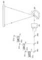
このプロジェクションディスプレイは、赤(R),緑(G),青(B)各色のレーザからなる光源200a,200b,200cと、各光源に対応して設けられた光スイッチング素子アレイ201a,201b,201c、ダイクロイックミラー202a,202b,202c、プロジェクションレンズ203、1軸スキャナとしてのガルバノミラー204および投射スクリーン205を備えている。なお、3原色は、赤,緑,青の他、シアン,マゼンダ,イエローとしてもよい。スイッチング素子アレイ201a,201b,201cはそれぞれ、上記スイッチング素子を紙面に対して垂直な方向に複数、必要画素数分、例えば1000個を1次元に配列したものであり、これによりライトバルブを構成している。
【0072】
このプロジェクションディスプレイでは、RGB各色の光源200a,200b,200cから出た光は、それぞれ光スイッチング素子アレイ201a,201b,201cに入射される。なお、この入射角は偏光の影響がでないように、なるべく0に近くし、垂直に入射させるようにすることが好ましい。各光スイッチング素子からの反射光P3は、ダイクロイックミラー202a,202b,202cによりプロジェクションレンズ203に集光される。プロジェクションレンズ203で集光された光は、ガルバノミラー204によりスキャンされ、投射スクリーン205上に2次元の画像として投影される。
【0073】
このように、このプロジェクションディスプレイでは、複数個の光スイッチング素子を1次元に配列し、RGBの光をそれぞれ照射し、スイッチング後の光を1軸スキャナにより走査することによって、2次元画像を表示することができる。
【0074】
また、本実施の形態では、低反射時の反射率を0.1%以下、高反射時の反射率を70%以上とすることができるので、1,000対1程度の高コントラストの表示を行うことができると共に、素子に対して光が垂直に入射する位置で特性を出すことができるので、光学系を組み立てる際に、偏光等を考慮にする必要がなく、構成が簡単である。
【0075】
以上実施の形態を挙げて本発明を説明したが、本発明は上記実施の形態および変形例に限定されるものではなく、種々変形可能である。例えば、上記実施の形態では、光源としてレーザを用いて一次元アレイ状のライトバルブを走査する構成のディスプレイについて説明したが、図16に示したように、二次元状に配列された光スイッチング装置206に白色光源207からの光を照射して投射スクリーン208に画像の表示を行う構成とすることもできる。
【0076】
また、上記実施の形態では、基板としてガラス基板を用いる例について説明したが、図17に示したように、例えば厚さ2mm以内の柔軟性を有する(フレキシブルな)基板209を用いたペーパ−状のディスプレイとし、直視により画像を見ることができるようにしてもよい。
【0077】
更に、上記実施の形態では、本発明の光学多層構造体をディスプレイに用いた例について説明したが、例えば光プリンタに用いて感光性ドラムへの画像の描きこみをする等、ディスプレイ以外の光プリンタなどの各種デバイスにも適用することも可能である。
【0078】
【発明の効果】
以上説明したように本発明の光学多層構造体および光スイッチング素子によれば、第1の層もしくは第1の層の代わりの基板の複素屈折率をN1(=n1−i・k1,n1は屈折率,k1は消衰係数,iは虚数単位)、第2の層若しくは透明層の屈折率をn2、入射媒質の屈折率を1.0としたとき、特定の条件を満たすように構成したので、間隙部の大きさを変化させることにより、入射した光の反射、透過若しくは吸収の量を変化させることができ、簡単な構成で、特に可視光領域においても、高速応答が可能になる。また、間隙部をなくして基板上に第1の層および第2の層をこの順で接する構造とすることにより、反射防止膜として利用することができる。加えて、第1の層の膜厚を厚くすることができるので、第1の層の電気抵抗が低減され、配線の信頼性が向上する。
【0079】
更に、基板や第1の層の選択に自由度があるため、光学多層構造体の製造方法として、例えば犠牲層にSiを用い、XeF2でドライエッチングする方法を適用することができ、開口度の高い素子を容易に作製することができる。
【0080】
また、本発明の画像表示装置によれば、本発明の光スイッチング素子を1次元に配列し、この1次元アレイ構造の光スイッチング装置を用いて画像表示を行うようにしたので、高コントラストの表示を行うことができると共に、素子に対して光が垂直に入射する位置で特性を出すことができるので、光学系を組み立てる場合に、偏光等を考慮にする必要がなく、構成が簡単となる。
【図面の簡単な説明】
【図1】 本発明の一実施の形態に係る光学多層構造体の間隙部が「λ/4」のときの構成を表す断面図である。
【図2】 図1に示した光学多層構造体の間隙部が「0」のときの構成を表す断面図である。
【図3】 図1に示した光学多層構造体の製造工程を説明するための断面図である。
【図4】 図3の工程に続く工程を説明するための断面図である。
【図5】 光学アドミッタンスダイアグラム上で、n2の屈折率を持つ透明な第2の層が、ダイアグラム上の(1,0)の点 (空気のアドミッタンス) を通る軌跡を表す図である。
【図6】 図1の光学多層構造体の変形例を表す図である。
【図7】 図1に示した光学多層構造体の一具体例の反射特性を表す図である。
【図8】 図7の例の低反射時の光学アドミッタンスを説明するための図である。
【図9】 図1の光学多層構造体の更に他の変形例を説明するための断面図である。
【図10】 光学多層構造体の静電気による駆動方法を説明するための断面図である。
【図11】 光学多層構造体の静電気による他の駆動方法を説明するための断面図である。
【図12】 光学多層構造体の静電気による更に他の駆動方法を説明するための断面図である。
【図13】 光学多層構造体の磁気による駆動方法を説明するための断面図である。
【図14】 光スイッチング装置の一例の構成を表す図である。
【図15】 ディスプレイの一例の構成を表す図である。
【図16】 ディスプレイの他の例を表す図である。
【図17】 ペーパー状ディスプレイの構成図である。[0001]
BACKGROUND OF THE INVENTION
The present invention relates to an optical multilayer structure having a function of reflecting, transmitting, or absorbing incident light, a manufacturing method thereof, an optical switching element, and an image display device.
[0002]
[Prior art]
In recent years, the importance of a display as a display device for video information has increased, and as an element for this display, an optical switching element (such as an optical communication, optical storage device, optical printer, etc.) that operates at high speed ( Development of light bulbs is demanded. Conventionally, as this type of element, those using liquid crystals, those using micromirrors (DMD; Digital Micro Miror Device, digital micromirror device, registered trademark of Texas Instruments), and those using diffraction gratings (GLV) : Grating Light Valve, manufactured by SLM (Silicon Light Machine).
[0003]
In GLV, a diffraction grating is produced with a MEMS (Micro Electro Mechanical Systems) structure, and a high-speed light switching element of 10 ns with an electrostatic force is realized. The DMD also performs switching by moving a mirror in the MEMS structure. Although a display such as a projector can be realized using these devices, the liquid crystal and the DMD have a low operation speed. Therefore, in order to realize a display as a light valve, a two-dimensional arrangement is required, and the structure becomes complicated. . On the other hand, since the GLV is a high-speed drive type, a projection display can be realized by scanning a one-dimensional array.
[0004]
However, since the GLV has a diffraction grating structure, there are complexity such that it is necessary to make six elements for one pixel and to combine the diffracted light emitted in two directions into one by some optical system.
[0005]
Examples of what can be realized with a simple configuration include those disclosed in US Pat. No. 5,589,974 and US Pat. No. 5,500,761. This light valve has a substrate (refractive index nS) With a refractive index of √nSThe light-transmitting thin film is provided. In this element, an optical signal is transmitted or reflected by driving the thin film using electrostatic force and changing the distance between the substrate and the thin film, that is, the size of the gap. Here, the refractive index of the thin film is the refractive index n of the substrate.S√nSIt is said that high contrast light modulation can be performed by satisfying such a relationship.
[0006]
[Problems to be solved by the invention]
However, in the element configured as described above, the refractive index n of the substrateSIf is not a large value such as “4”, there is a problem that it cannot be realized in the visible light region. That is, when considering that it is a structure as a light-transmitting thin film, silicon nitride (SiThreeNFour) (Refractive index n = 2.0) is desirable, in which case the refractive index n of the substrateS= 4. In the visible region, such material options are narrow. Communication wavelengths such as infrared light can be realized by using germanium (Ge) (n = 4), silicon (Si) (n≈4), or the like.
[0007]
Further, in a light valve disclosed in US Pat. No. 5,500,761, etc., silicon nitride (Si) is formed on a silicon substrate with a gap therebetween.ThreeNFour) And other structural materials. However, in this structure, the sacrificial layer is formed of silicon (Si), which is now widely recognized as dry etching of the sacrificial layer, and is formed of xenon difluoride (XeF).2Etching method cannot be used. This is because the substrate is also made of Si and cannot be selected from the sacrifice layer. Therefore, it seems that other methods such as wet etching are used in the above structure. In wet etching, it is difficult for the etching solution to enter the gap of about λ / 4 and circulate smoothly, and etching cannot be performed, or the structural material on the sacrificial layer is broken during drying due to the surface tension of the solution. Thus, it is difficult to produce a desired structure. It should be noted that if the opening area is reduced by reducing the relative area of the parts to be an optical switch, it can be realized by a process such as wet etching, but for image display, the opening degree tends to be increased. I want to reduce the number of parts that go into. Therefore, dry etching is more suitable than wet etching. However, when the substrate is formed of Si as described above, the sacrificial layer is formed of Si, and this is converted into XeF.2There is a problem that the etching method cannot be applied.
[0008]
The present invention has been made in view of such a problem, and a first object thereof is a simple configuration, a small size and a light weight, a degree of freedom in selection of constituent materials, and high speed even in the visible light region. An object of the present invention is to provide an optical multilayer structure that can respond and can be suitably used for an image display device or the like.
[0009]
The second object of the present invention is to form a sacrificial layer of Si in the gap forming step and2It is an object of the present invention to provide a method for manufacturing an optical multilayer structure that can be applied to dry etching using, and can easily produce an optical multilayer structure having a high aperture.
[0010]
Furthermore, a third object of the present invention is to provide an optical switching element and an image display device capable of high-speed response using the optical multilayer structure.
[0011]
[Means for Solving the Problems]
The first optical multilayer structure according to the present invention has, on the substrate, a first layer that absorbs light, a size capable of causing a light interference phenomenon, and a size of λ / 4 (λ is incident). The first layer has a structure in which a gap portion that is variable between an odd multiple of the wavelength of light) and an even multiple of λ / 4 (including 0) and a transparent second layer are arranged in this order,N satisfying number (9)1(= N1-I ・ k1, N1Is the refractive index, k1Is thick enough to make the optical information of the substrate invisible, with a material having a complex refractive index of (extinction coefficient, i is an imaginary unit)
The second layer is n satisfying the number (9)2Formed of a material having a refractive index ofIs.
[Equation 9]
[0012]
The second optical multilayer structure according to the present invention has a size capable of causing a light interference phenomenon on a light-absorbing substrate and has a size of λ / 4 (λ is the wavelength of incident light). An optical multilayer structure having a structure in which gaps variable between an odd multiple and an even multiple of λ / 4 (including 0) and a transparent layer are arranged in this order,N satisfying number (9)1(= N1-I ・ k1, N1Is the refractive index, k1N is an extinction coefficient, i is an imaginary number unit), and a transparent layer is formed by satisfying the number (9).2Formed of a material having a refractive index ofIs.
[0013]
A first optical switching element according to the present invention includes the first optical multilayer structure according to the present invention and drive means for changing the optical size of the gap portion in the optical multilayer structure. is there.
[0014]
A second optical switching element according to the present invention includes the second optical multilayer structure according to the present invention and driving means for changing the optical size of the gap portion in the optical multilayer structure. is there.
[0015]
A first image display device according to the present invention includes a plurality of the first optical switching elements according to the present invention arranged one-dimensionally or two-dimensionally, irradiated with light of three primary colors, and scanned by a scanner. A two-dimensional image is displayed.
[0016]
A second image display device according to the present invention includes a plurality of second optical switching elements according to the present invention arranged one-dimensionally or two-dimensionally, irradiating light of three primary colors, and scanning with a scanner. A two-dimensional image is displayed.
[0017]
In the first and second optical multilayer structures according to the present invention, the size of the gap is set to an odd multiple of “λ / 4” (λ is the design wavelength of incident light) and an even multiple of “λ / 4” (0 The amount of reflection, transmission or absorption of incident light changes in a binary or continuous manner.
[0018]
In the first and second optical switching elements according to the present invention, the switching operation is performed on the incident light by changing the optical size of the gap portion of the optical multilayer structure by the driving means.
[0019]
In the first and second image display devices according to the present invention, a two-dimensional image is displayed by irradiating light to the plurality of optical switching elements of the present invention arranged one-dimensionally or two-dimensionally.
[0020]
DETAILED DESCRIPTION OF THE INVENTION
Hereinafter, embodiments of the present invention will be described in detail with reference to the drawings.
[0021]
1 and 2 show a basic configuration of an
[0022]
The
[0023]
Here, in this embodiment, the complex refractive index of the
[0024]
[Expression 10]
The
[0026]
The
[0027]
The
[0028]
The
[0029]
Physical thickness d of the
[0030]
Optical thickness n of the
[0031]
In addition, “λ / 4” in the notation in the present specification may not be strictly “λ / 4” but may be a value in the vicinity thereof. This is because, for example, the optical film thickness of one layer becomes thicker than λ / 4, so that the other layer can be made thinner, and the refractive index slightly deviates from the above equation (8). This is because there are cases where the film thickness can be adjusted. Therefore, in this specification, the expression “λ / 4” includes the case of “approximately λ / 4”.
[0032]
The
[0033]
The
[0034]
The optical size of the
[0035]
The
[0036]
Next, after removing the
[0037]
In the
[0038]
Next, the significance of the formula (5) will be described with reference to FIGS.
[0039]
The filter characteristics of the
[0040]
On the optical admittance diagram, n2A transparent second layer having an index of refraction of Fig. 5 shows a trajectory passing through a point (1,0) (air admittance) on the diagram, as shown in FIG. That is, 1 and n on the real axis Re (Y)22Through the center (n22+1) / 2 arc. Here, when the
[0041]
That is, in this
[0042]
If the
[0043]
As a combination of materials for such an optical multilayer structure, it is sufficient if the above-mentioned restrictions are satisfied, and the degree of freedom of selection is wide. Table 1 shows an example. Note that tantalum nitride and ITO are actual measured values actually deposited by the present inventors, and SiThreeNFourIs a general value.
[0044]
[Table 1]
Here, TaN is used as the first layer 11.XLayer, air layer (n = 1.00) as the
[0046]
FIG. 7 shows the result of simulating the relationship between the wavelength of incident light (design wavelength 550 nm) and the reflectance in such a configuration. Here, A is the characteristic when the optical film thickness of the gap (air layer) is “0” (low reflection side), and B is the characteristic when the optical film thickness is “λ / 4” (138 nm) (high reflection side). Represents. FIG. 8 shows a composite optical admittance diagram at the time of low reflection, and it can be seen that the composite optical admittance ends in the vicinity of 1.0. As described above, nitride is preferable as the material of the
[0047]
[Table 2]
As described above, in this embodiment, even in the visible light region such as 550 nm, the reflectance at the time of low reflection can be almost 0, and the reflectance at the time of high reflection can be 70% or more. Can be done. Moreover, since the configuration is simple, it can be more easily produced than a diffraction grating structure such as GLV or a complicated three-dimensional structure such as DMD. In addition, the GLV requires six grid-like ribbons for one pixel, but in this embodiment, only one is required, so that the configuration is simple and it is possible to make the ribbon small. Further, since the moving range of the movable part is at most “λ / 2”, a high-speed response of 10 ns level is possible. Therefore, when used as a light valve for display applications, it can be realized with a simple configuration of a one-dimensional array as will be described later.
[0049]
Furthermore, the
[0050]
In the present embodiment, since the refractive indexes of the
[0051]
Note that the same applicant as the present applicant firstly has a first layer that absorbs light on the substrate, a gap that has a size capable of causing a light interference phenomenon, and whose size is variable, and An optical multilayer structure having a structure in which a second layer is provided has been proposed (Japanese Patent Application No. 2000-219599). This optical multilayer structure has a simple configuration, has a degree of freedom in selection of constituent materials, can respond at high speed even in the visible light region, and can be suitably used for an image display device or the like. However, in order to realize this optical multilayer structure, the film thickness of the first layer (conductive layer) is limited, and the film thickness is as thin as about 10 nm. When the conductive layer has such a film thickness, the electrical resistance sometimes increases. On the other hand, in this embodiment, since the thickness of the first layer (conductive layer) is sufficiently thick so that the optical information of the substrate cannot be seen, the electrical resistance is reduced and the wiring is Reliability is improved.
[0052]
As described above, by using the
[0053]
In the above embodiment, the gap portion of the
[0054]
In this optical multilayer structure, the intermediate
[0055]
[Driving method]
Next, specific means for changing the size of the
[0056]
FIG. 10 shows an example in which the optical multilayer structure is driven by static electricity. In this optical multilayer structure,
[0057]
In this optical multilayer structure, the optical film thickness of the
[0058]
In addition, the method shown in FIGS. 11 and 12 may be used to drive the optical multilayer structure with static electricity. In the
[0059]
In this optical multilayer structure, the optical film thickness of the
[0060]
In the optical multilayer structure shown in FIG. 12, a tantalum (Ta) film, for example, is disposed as the conductive
[0061]
In addition to such static electricity, the optical multilayer structure can be driven by various methods such as a method using a micromachine such as a toggle mechanism or a piezoelectric element, a method using a magnetic force, and a method using a shape memory alloy. FIGS. 13A and 13B show a mode of driving using magnetic force. In this optical multilayer structure, a
[0062]
[Optical switching device]
FIG. 14 shows a configuration of an optical switching device 100 using the
[0063]
On the
[0064]
The
[0065]
In this optical switching device 100, TaNXWhen the potential is set to 0 V by grounding the
[0066]
Next, when the transparent
[0067]
Thus, in the present embodiment, the incident light P in each of the
[0068]
In these
[0069]
In addition, in the present embodiment, if a plurality of optical switching elements are assigned to one pixel, they can be independently driven. Therefore, when performing gradation display of image display as an image display device, a method using time division In addition to this, gradation display by area is also possible.
[0070]
(Image display device)
FIG. 15 shows a configuration of a projection display as an example of an image display device using the optical switching device 100. Here, the reflected light P from the
[0071]
This projection display includes
[0072]
In this projection display, the light emitted from the
[0073]
As described above, in this projection display, a plurality of optical switching elements are arranged in a one-dimensional manner, RGB light is respectively irradiated, and the light after switching is scanned by a one-axis scanner to display a two-dimensional image. be able to.
[0074]
In the present embodiment, the reflectance at the time of low reflection can be 0.1% or less, and the reflectance at the time of high reflection can be 70% or more. Therefore, a high contrast display of about 1,000 to 1 can be achieved. In addition, since the characteristics can be obtained at a position where the light is perpendicularly incident on the element, it is not necessary to consider polarization or the like when assembling the optical system, and the configuration is simple.
[0075]
Although the present invention has been described with reference to the embodiments, the present invention is not limited to the above-described embodiments and modifications, and various modifications can be made. For example, in the above-described embodiment, the display configured to scan a one-dimensional array of light valves using a laser as a light source has been described. However, as shown in FIG. 16, an optical switching device arranged in a two-dimensional manner. A configuration may also be adopted in which light is emitted from the
[0076]
In the above-described embodiment, an example in which a glass substrate is used as the substrate has been described. However, as illustrated in FIG. 17, for example, a paper shape using a
[0077]
Furthermore, in the above-described embodiment, an example in which the optical multilayer structure of the present invention is used for a display has been described. However, for example, an optical printer other than a display can be used such as drawing an image on a photosensitive drum using an optical printer. It is also possible to apply to various devices such as.
[0078]
【The invention's effect】
As described above, according to the optical multilayer structure and the optical switching element of the present invention, the complex refractive index of the first layer or the substrate instead of the first layer is N1(= N1-I ・ k1, N1Is the refractive index, k1Is the extinction coefficient, i is the imaginary unit), and the refractive index of the second layer or transparent layer is n2When the refractive index of the incident medium is 1.0, it is configured to satisfy a specific condition. Therefore, the amount of reflection, transmission, or absorption of incident light is changed by changing the size of the gap. Therefore, a high-speed response is possible with a simple configuration, particularly in the visible light region. In addition, by providing a structure in which the first layer and the second layer are in contact with each other in this order on the substrate by eliminating the gap, it can be used as an antireflection film. In addition, since the thickness of the first layer can be increased, the electrical resistance of the first layer is reduced and the reliability of the wiring is improved.
[0079]
Furthermore, since there is a degree of freedom in selecting the substrate and the first layer, as a method for manufacturing an optical multilayer structure, for example, Si is used as a sacrificial layer, and XeF2Thus, a dry etching method can be applied, and an element with a high aperture can be easily manufactured.
[0080]
Further, according to the image display device of the present invention, the optical switching elements of the present invention are arranged one-dimensionally, and image display is performed using the optical switching device having this one-dimensional array structure. In addition, since the characteristics can be obtained at a position where light is incident perpendicularly to the element, it is not necessary to consider polarization or the like when assembling the optical system, and the configuration is simplified.
[Brief description of the drawings]
FIG. 1 is a cross-sectional view illustrating a configuration when a gap portion of an optical multilayer structure according to an embodiment of the present invention is “λ / 4”.
2 is a cross-sectional view illustrating a configuration when a gap portion of the optical multilayer structure illustrated in FIG. 1 is “0”. FIG.
3 is a cross-sectional view for explaining a manufacturing process of the optical multilayer structure shown in FIG. 1. FIG.
4 is a view for explaining a step that follows the step of FIG. 3;Cross sectionIt is.
FIG. 5 shows n on the optical admittance diagram.2FIG. 3 is a diagram showing a trajectory passing through a point (1, 0) (air admittance) on a diagram by a transparent second layer having a refractive index of λ.
6 is a diagram showing a modification of the optical multilayer structure in FIG. 1. FIG.
FIG. 7 is a diagram showing the reflection characteristics of a specific example of the optical multilayer structure shown in FIG.
FIG. 87It is a figure for demonstrating the optical admittance at the time of the low reflection of the example of.
FIG. 9 is a cross-sectional view for explaining still another modification of the optical multilayer structure of FIG.
FIG. 10 is a cross-sectional view for explaining a method of driving the optical multilayer structure by static electricity.
FIG. 11 is a cross-sectional view for explaining another driving method by static electricity of the optical multilayer structure.
FIG. 12 is a cross-sectional view for explaining still another driving method by static electricity of the optical multilayer structure.
FIG. 13 is a cross-sectional view for explaining a magnetic driving method of the optical multilayer structure.
FIG. 14 is a diagram illustrating a configuration of an example of an optical switching device.
FIG. 15 is a diagram illustrating a configuration of an example of a display.
FIG. 16 is a diagram illustrating another example of the display.
FIG. 17 is a configuration diagram of a paper-like display.
Claims (21)
Translated fromJapanese前記第1の層を、数(1)を満たすN1(=n1−i・k1,n1は屈折率,k1は消衰係数,iは虚数単位)の複素屈折率を有する材料により前記基板の光学的情報が見えなくなる程度に厚く形成すると共に、
前記第2の層を、数(1)を満たすn2の屈折率を有する材料により形成した
ことを特徴とする光学多層構造体。The first layer having light absorption on the substrate has a size capable of causing an optical interference phenomenon, and the size is an odd multiple of λ / 4 (λ is the wavelength of incident light) and λ / 4. An optical multilayer structure having a structure in which a gap portion that is variable between an even number of times (including 0) and a transparent second layer are arranged in this order,
The first layeris a material having a complex refractive index ofN1(= n1−i · k1, where n1is a refractive index, k1is an extinction coefficient, and i is an imaginary unit)satisfying the number (1).And so thick that the optical information of the substrate becomes invisible,
The second layer isformed of a material having a refractive index ofn2satisfying the number (1).
An optical multilayer structure characterized by that.
前記基板を、数(2)を満たすN1(=n1−i・k1,n1は屈折率,k1は消衰係数,iは虚数単位)の複素屈折率を有する材料により形成すると共に、
前記透明層を、数(2)を満たすn2の屈折率を有する材料により形成した
ことを特徴とする光学多層構造体。On a substrate that absorbs light, the substrate has a size capable of causing a light interference phenomenon, and the size is an odd multiple of λ / 4 (λ is the wavelength of incident light) and an even multiple of λ / 4 (zero). An optical multilayer structure having a structure in which a gap portion that is variable between the transparent layer and the transparent layer is disposed in this order,
The substrateisformed of a material having a complex refractive index ofN1(= n1−i · k1, where n1is a refractive index, k1is an extinction coefficient, and i is an imaginary unit)satisfying the number (2).With
The transparent layer isformed of a material having a refractive index ofn2that satisfies the number (2).
An optical multilayer structure characterized by that.
ことを特徴とする請求項1または2に記載の光学多層構造体。The optical multilayer structure according to claim 1 or 2, wherein the substrate is made of a transparent material or a semi-transparent material.
記駆動手段によって前記間隙部の大きさを2値的あるいは連続的に変化させることで、入
射光の反射、透過若しくは吸収の量を2値的あるいは連続的に変化させる
ことを特徴とする請求項1または2記載の光学多層構造体。Furthermore, it has a drive means for changing the optical size of the gap, and the drive means can change the size of the gap in a binary or continuous manner to reflect, transmit or transmit incident light. The optical multilayer structure according to claim 1 or 2, wherein the amount of absorption is changed binaryly or continuously.
ことを特徴とする請求項1または2に記載の光学多層構造体。3. The composite layer according to claim 1, wherein at least one of the first layer and the second layer is a composite layer including two or more layers having different optical characteristics. Optical multilayer structure.
ことを特徴とする請求項1または2に記載の光学多層構造体。The optical multilayer structure according to claim 1 or 2, wherein the first layer is formed of a nitride material.
ことを特徴とする請求項6に記載の光学多層構造体。The optical multilayer structure according to claim 6, wherein the nitride material is formed of any one of titanium nitride, tantalum nitride, hafnium nitride, and zirconium nitride.
ことを特徴とする請求項4記載の光学多層構造体。At least one of the first layer and the second layer partially includes a transparent conductive film, and the driving unit is configured to generate the gap portion by electrostatic force generated by applying a voltage to the transparent conductive film. The optical multilayer structure according to claim 4, wherein the optical size of the optical multilayer structure is changed.
ことを特徴とする請求項8記載の光学多層構造体。The optical multilayer structure according to claim 8, wherein the transparent conductive film is formed of any one of ITO, SnO2 and ZnO.
ことを特徴とする請求項1または2に記載の光学多層構造体。3. The optical multilayer structure according to claim 1, wherein an optical film thickness of the second layer is equal to or less than λ / 4 (λ is a design wavelength of incident light). 4.
ことを特徴とする請求項4記載の光学多層構造体。The optical multilayer structure according to claim 4, wherein the driving unit is configured to change an optical size of the gap using magnetic force.
前記第1の層を、数(3)を満たすN1(=n1−i・k1,n1は屈折率,k1は消衰係数,iは虚数単位)の複素屈折率を有する材料により前記基板の光学的情報が見えなくなる程度に厚く形成すると共に、
前記第2の層を、数(3)を満たすn2の屈折率を有する材料により形成した
ことを特徴とする光スイッチング素子。The first layer having light absorption on the substrate has a size capable of causing an optical interference phenomenon, and the size is an odd multiple of λ / 4 (λ is the wavelength of incident light) and λ / 4. An optical multilayer structure having a structure in which a gap portion that is variable between an even number of times (including 0) and a transparent second layer are arranged in this order, and an optical size of the gap portion Drive means for changing,
A material having a complex refractive index ofN1(= n1−i · k1, where n1is a refractive index, k1is an extinction coefficient, and i is an imaginary unit)satisfying the number (3) for the first layerAnd so thick that the optical information of the substrate becomes invisible,
The second layer isformed of a material having a refractive index ofn2that satisfies the number (3).
An optical switching element.
前記基板を、数(4)を満たすN1(=n1−i・k1,n1は屈折率,k1は消衰係数,iは虚数単位)の複素屈折率を有する材料により形成すると共に、
前記透明層を、数(4)を満たすn2の屈折率を有する材料により形成した
ことを特徴とする光スイッチング素子。On a substrate that absorbs light, the substrate has a size capable of causing a light interference phenomenon, and the size is an odd multiple of λ / 4 (λ is the wavelength of incident light) and an even multiple of λ / 4 (zero). And an optical multilayer structure having a structure in which transparent layers are arranged in this order, and driving means for changing the optical size of the gap. ,
The substrateisformed of a material having a complex refractive index ofN1(= n1−i · k1, where n1is a refractive index, k1is an extinction coefficient, and i is an imaginary unit)satisfying theequation(4).With
The transparent layer isformed of a material having a refractive index ofn2that satisfies the number (4).
An optical switching element.
前記光スイッチング素子が、基板上に、光の吸収のある第1の層、光の干渉現象を起こし得る大きさを有すると共にその大きさが、λ/4(λは入射光の波長)の奇数倍とλ/4の偶数倍(0を含む)との間で可変な間隙部、および透明な第2の層をこの順で配設した構造を備えた光学多層構造体と、前記間隙部の光学的な大きさを変化させるための駆動手段とを備え、
前記第1の層を、数(5)を満たすN1(=n1−i・k1,n1は屈折率,k1は消衰係数,iは虚数単位)の複素屈折率を有する材料により前記基板の光学的情報が見えなくなる程度に厚く形成すると共に、
前記第2の層を、数(5)を満たすn2の屈折率を有する材料により形成した
ことを特徴とする画像表示装置。An image display device that displays a two-dimensional image by irradiating light to a plurality of optical switching elements arranged one-dimensionally or two-dimensionally,
The optical switching element has a first layer that absorbs light on the substrate and has a size capable of causing a light interference phenomenon, and the size is an odd number of λ / 4 (λ is the wavelength of incident light). An optical multilayer structure having a structure in which a gap portion that is variable between a multiple of λ / 4 and an even multiple of λ / 4 (including 0) and a transparent second layer are arranged in this order, Driving means for changing the optical size,
A material having a complex refractive index ofN1(= n1−i · k1, where n1is a refractive index, k1is an extinction coefficient, and i is an imaginary unit)satisfying the number (5) for the first layerAnd so thick that the optical information of the substrate becomes invisible,
The second layer isformed of a material having a refractive index ofn2that satisfies the number (5).
An image display device characterized by that.
前記光スイッチング素子が、光の吸収のある基板上に、光の干渉現象を起こし得る大きさを有すると共にその大きさが、λ/4(λは入射光の波長)の奇数倍とλ/4の偶数倍(0を含む)との間で可変な間隙部、および透明層をこの順で配設した構造を備えた光学多層構造体と、前記間隙部の光学的な大きさを変化させるための駆動手段とを備え、
前記基板を、数(6)を満たすN1(=n1−i・k1,n1は屈折率,k1は消衰係数,iは虚数単位)の複素屈折率を有する材料により形成すると共に、
前記透明層を、数(6)を満たすn2の屈折率を有する材料により形成した
ことを特徴とする画像表示装置。An image display device that displays a two-dimensional image by irradiating light to a plurality of optical switching elements arranged one-dimensionally or two-dimensionally,
The optical switching element has a size capable of causing an optical interference phenomenon on a light-absorbing substrate, and the size is an odd multiple of λ / 4 (λ is the wavelength of incident light) and λ / 4. An optical multilayer structure having a structure in which a gap portion that is variable to an even number of times (including 0) and a transparent layer are arranged in this order, and an optical size of the gap portion is changed. Driving means,
The substrateisformed of a material having a complex refractive index ofN1(= n1−i · k1, where n1is a refractive index, k1is an extinction coefficient, and i is an imaginary unit)satisfying theequation(6).With
The transparent layer isformed of a material having a refractive index ofn2that satisfies the number (6).
An image display device characterized by that.
前記基板上に前記第1の層を形成した後、前記第1の層上に犠牲層を形成し、前記犠牲層上に前記第2の層を形成し、その後、前記犠牲層を選択的に除去することにより前記間隙部を形成する工程を
含むことを特徴とする光学多層構造体の製造方法。The first layer having light absorption on the substrate has a size capable of causing an optical interference phenomenon, and the size is an odd multiple of λ / 4 (λ is the wavelength of incident light) and λ / 4.N1 that has a structure in which a gap portion that is variable with an even number of times (including 0) and a transparent second layer are arranged in this order, and the first layersatisfies N (7)(= N1−i · k1, where n1is the refractive index, k1is the extinction coefficient, and i is the imaginary unit) The material having a complex refractive index is formed so thick that the optical information of the substrate cannot be seen. And the second layer is a method for producingan optical multilayer structureformed of a material having a refractive index ofn2satisfying the number (7) ,
After forming the first layer on the substrate, a sacrificial layer is formed on the first layer, the second layer is formed on the sacrificial layer, and then the sacrificial layer is selectively formed A method for producing an optical multilayer structure comprising the step of forming the gap portion by removing.
前記基板上に犠牲層を形成し、前記犠牲層上に前記透明層を形成し、その後、前記犠牲層を選択的に除去することにより前記間隙部を形成する工程を
含むことを特徴とする光学多層構造体の製造方法。On a substrate that absorbs light, the substrate has a size capable of causing a light interference phenomenon, and the size is an odd multiple of λ / 4 (λ is the wavelength of incident light) and an even multiple of λ / 4 (zero). variable gap between inclusive), and has a structure provided a transparent layer in this order, thesubstrate,n1satisfy formula(8) (= n 1 -i · k 1, n 1Is a refractive index, k1is an extinction coefficient, i is an imaginary unit), and the transparent layer isformed of a material having a refractive index ofn2satisfying the number (8).A method for producingan optical multilayer structure, comprising:
Forming a gap layer by forming a sacrificial layer on the substrate, forming the transparent layer on the sacrificial layer, and then selectively removing the sacrificial layer. A method for producing a multilayer structure.
ことを特徴とする請求項16または17記載の光学多層構造体の製造方法。The method for producing an optical multilayer structure according to claim 16 or 17, wherein the selective removal of the sacrificial layer is performed by etching with a dry gas.
ことを特徴とする請求項16記載の光学多層構造体の製造方法。The optical multilayer structure according to claim 16, wherein the sacrificial layer is selectively removed by etching with a dry gas, and the first layer is formed of a material resistant to the dry gas. Production method.
ことを特徴とする請求項17記載の光学多層構造体の製造方法。The method for manufacturing an optical multilayer structure according to claim 17, wherein the sacrificial layer is selectively removed by etching with a dry gas, and the substrate is formed of a material resistant to the dry gas.
ことを特徴とする請求項19または20記載の光学多層構造体の製造方法。The method for manufacturing an optical multilayer structure according to claim 19 or 20, wherein the sacrificial layer is formed of silicon (Si) and xenon difluoride (XeF2 ) is used as an etching gas.
Priority Applications (6)
| Application Number | Priority Date | Filing Date | Title |
|---|---|---|---|
| JP2001212251AJP4032216B2 (en) | 2001-07-12 | 2001-07-12 | OPTICAL MULTILAYER STRUCTURE, ITS MANUFACTURING METHOD, OPTICAL SWITCHING DEVICE, AND IMAGE DISPLAY DEVICE |
| CNB028025008ACN1266509C (en) | 2001-07-12 | 2002-07-12 | Optical multilayer structure and its production method, optical switching device, and image display |
| US10/380,224US6850365B2 (en) | 2001-07-12 | 2002-07-12 | Optical multilayer structure and its production method, optical switching device, and image display |
| KR1020037003395AKR100937839B1 (en) | 2001-07-12 | 2002-07-12 | Optical multilayer structure and manufacturing method thereof, and optical switching element and image display device |
| EP02746024.5AEP1406109B1 (en) | 2001-07-12 | 2002-07-12 | Optical multilayer structure and its production method, optical switching device, and image display |
| PCT/JP2002/007124WO2003007050A1 (en) | 2001-07-12 | 2002-07-12 | Optical multilayer structure and its production method, optical switching device, and image display |
Applications Claiming Priority (1)
| Application Number | Priority Date | Filing Date | Title |
|---|---|---|---|
| JP2001212251AJP4032216B2 (en) | 2001-07-12 | 2001-07-12 | OPTICAL MULTILAYER STRUCTURE, ITS MANUFACTURING METHOD, OPTICAL SWITCHING DEVICE, AND IMAGE DISPLAY DEVICE |
Publications (3)
| Publication Number | Publication Date |
|---|---|
| JP2003029169A JP2003029169A (en) | 2003-01-29 |
| JP2003029169A5 JP2003029169A5 (en) | 2004-08-26 |
| JP4032216B2true JP4032216B2 (en) | 2008-01-16 |
Family
ID=19047443
Family Applications (1)
| Application Number | Title | Priority Date | Filing Date |
|---|---|---|---|
| JP2001212251AExpired - Fee RelatedJP4032216B2 (en) | 2001-07-12 | 2001-07-12 | OPTICAL MULTILAYER STRUCTURE, ITS MANUFACTURING METHOD, OPTICAL SWITCHING DEVICE, AND IMAGE DISPLAY DEVICE |
Country Status (6)
| Country | Link |
|---|---|
| US (1) | US6850365B2 (en) |
| EP (1) | EP1406109B1 (en) |
| JP (1) | JP4032216B2 (en) |
| KR (1) | KR100937839B1 (en) |
| CN (1) | CN1266509C (en) |
| WO (1) | WO2003007050A1 (en) |
Families Citing this family (182)
| Publication number | Priority date | Publication date | Assignee | Title |
|---|---|---|---|---|
| US7297471B1 (en) | 2003-04-15 | 2007-11-20 | Idc, Llc | Method for manufacturing an array of interferometric modulators |
| US7550794B2 (en)* | 2002-09-20 | 2009-06-23 | Idc, Llc | Micromechanical systems device comprising a displaceable electrode and a charge-trapping layer |
| US7123216B1 (en)* | 1994-05-05 | 2006-10-17 | Idc, Llc | Photonic MEMS and structures |
| US7471444B2 (en)* | 1996-12-19 | 2008-12-30 | Idc, Llc | Interferometric modulation of radiation |
| WO1999052006A2 (en)* | 1998-04-08 | 1999-10-14 | Etalon, Inc. | Interferometric modulation of radiation |
| US7532377B2 (en) | 1998-04-08 | 2009-05-12 | Idc, Llc | Movable micro-electromechanical device |
| WO2003007049A1 (en) | 1999-10-05 | 2003-01-23 | Iridigm Display Corporation | Photonic mems and structures |
| US6960305B2 (en)* | 1999-10-26 | 2005-11-01 | Reflectivity, Inc | Methods for forming and releasing microelectromechanical structures |
| US6794119B2 (en)* | 2002-02-12 | 2004-09-21 | Iridigm Display Corporation | Method for fabricating a structure for a microelectromechanical systems (MEMS) device |
| US6574033B1 (en) | 2002-02-27 | 2003-06-03 | Iridigm Display Corporation | Microelectromechanical systems device and method for fabricating same |
| US7781850B2 (en)* | 2002-09-20 | 2010-08-24 | Qualcomm Mems Technologies, Inc. | Controlling electromechanical behavior of structures within a microelectromechanical systems device |
| TW200413810A (en) | 2003-01-29 | 2004-08-01 | Prime View Int Co Ltd | Light interference display panel and its manufacturing method |
| TW594360B (en)* | 2003-04-21 | 2004-06-21 | Prime View Int Corp Ltd | A method for fabricating an interference display cell |
| TW570896B (en) | 2003-05-26 | 2004-01-11 | Prime View Int Co Ltd | A method for fabricating an interference display cell |
| US7221495B2 (en)* | 2003-06-24 | 2007-05-22 | Idc Llc | Thin film precursor stack for MEMS manufacturing |
| TW200506479A (en)* | 2003-08-15 | 2005-02-16 | Prime View Int Co Ltd | Color changeable pixel for an interference display |
| TWI231865B (en)* | 2003-08-26 | 2005-05-01 | Prime View Int Co Ltd | An interference display cell and fabrication method thereof |
| TWI232333B (en) | 2003-09-03 | 2005-05-11 | Prime View Int Co Ltd | Display unit using interferometric modulation and manufacturing method thereof |
| TW593126B (en) | 2003-09-30 | 2004-06-21 | Prime View Int Co Ltd | A structure of a micro electro mechanical system and manufacturing the same |
| JP3770326B2 (en) | 2003-10-01 | 2006-04-26 | セイコーエプソン株式会社 | Analysis equipment |
| US7142346B2 (en)* | 2003-12-09 | 2006-11-28 | Idc, Llc | System and method for addressing a MEMS display |
| US7161728B2 (en)* | 2003-12-09 | 2007-01-09 | Idc, Llc | Area array modulation and lead reduction in interferometric modulators |
| KR100577696B1 (en)* | 2003-12-15 | 2006-05-10 | 삼성전자주식회사 | Image liquid crystal display device that can have a uniform cell gap |
| JP3924758B2 (en)* | 2004-01-23 | 2007-06-06 | 下山 勲 | Coloring structure and display device |
| US7855824B2 (en)* | 2004-03-06 | 2010-12-21 | Qualcomm Mems Technologies, Inc. | Method and system for color optimization in a display |
| DE102004013851B4 (en)* | 2004-03-20 | 2021-06-17 | Robert Bosch Gmbh | Process for the production of an interference filter from alternating air-semiconductor layer systems as well as an infrared filter produced with the process |
| US7476327B2 (en)* | 2004-05-04 | 2009-01-13 | Idc, Llc | Method of manufacture for microelectromechanical devices |
| TWI233916B (en)* | 2004-07-09 | 2005-06-11 | Prime View Int Co Ltd | A structure of a micro electro mechanical system |
| EP2246726B1 (en)* | 2004-07-29 | 2013-04-03 | QUALCOMM MEMS Technologies, Inc. | System and method for micro-electromechanical operating of an interferometric modulator |
| US7515147B2 (en)* | 2004-08-27 | 2009-04-07 | Idc, Llc | Staggered column drive circuit systems and methods |
| US7551159B2 (en)* | 2004-08-27 | 2009-06-23 | Idc, Llc | System and method of sensing actuation and release voltages of an interferometric modulator |
| US7560299B2 (en)* | 2004-08-27 | 2009-07-14 | Idc, Llc | Systems and methods of actuating MEMS display elements |
| US7889163B2 (en) | 2004-08-27 | 2011-02-15 | Qualcomm Mems Technologies, Inc. | Drive method for MEMS devices |
| US7499208B2 (en)* | 2004-08-27 | 2009-03-03 | Udc, Llc | Current mode display driver circuit realization feature |
| US7161730B2 (en) | 2004-09-27 | 2007-01-09 | Idc, Llc | System and method for providing thermal compensation for an interferometric modulator display |
| US7369294B2 (en)* | 2004-09-27 | 2008-05-06 | Idc, Llc | Ornamental display device |
| US8004504B2 (en)* | 2004-09-27 | 2011-08-23 | Qualcomm Mems Technologies, Inc. | Reduced capacitance display element |
| US7429334B2 (en) | 2004-09-27 | 2008-09-30 | Idc, Llc | Methods of fabricating interferometric modulators by selectively removing a material |
| US20060065622A1 (en)* | 2004-09-27 | 2006-03-30 | Floyd Philip D | Method and system for xenon fluoride etching with enhanced efficiency |
| US7564612B2 (en)* | 2004-09-27 | 2009-07-21 | Idc, Llc | Photonic MEMS and structures |
| US7898521B2 (en)* | 2004-09-27 | 2011-03-01 | Qualcomm Mems Technologies, Inc. | Device and method for wavelength filtering |
| US7492502B2 (en)* | 2004-09-27 | 2009-02-17 | Idc, Llc | Method of fabricating a free-standing microstructure |
| US7612932B2 (en)* | 2004-09-27 | 2009-11-03 | Idc, Llc | Microelectromechanical device with optical function separated from mechanical and electrical function |
| US7373026B2 (en)* | 2004-09-27 | 2008-05-13 | Idc, Llc | MEMS device fabricated on a pre-patterned substrate |
| US20060066594A1 (en)* | 2004-09-27 | 2006-03-30 | Karen Tyger | Systems and methods for driving a bi-stable display element |
| US7372613B2 (en)* | 2004-09-27 | 2008-05-13 | Idc, Llc | Method and device for multistate interferometric light modulation |
| US7843410B2 (en) | 2004-09-27 | 2010-11-30 | Qualcomm Mems Technologies, Inc. | Method and device for electrically programmable display |
| US7405861B2 (en)* | 2004-09-27 | 2008-07-29 | Idc, Llc | Method and device for protecting interferometric modulators from electrostatic discharge |
| US8878825B2 (en)* | 2004-09-27 | 2014-11-04 | Qualcomm Mems Technologies, Inc. | System and method for providing a variable refresh rate of an interferometric modulator display |
| US7136213B2 (en) | 2004-09-27 | 2006-11-14 | Idc, Llc | Interferometric modulators having charge persistence |
| US7527995B2 (en)* | 2004-09-27 | 2009-05-05 | Qualcomm Mems Technologies, Inc. | Method of making prestructure for MEMS systems |
| US7626581B2 (en)* | 2004-09-27 | 2009-12-01 | Idc, Llc | Device and method for display memory using manipulation of mechanical response |
| US20060065366A1 (en)* | 2004-09-27 | 2006-03-30 | Cummings William J | Portable etch chamber |
| US7583429B2 (en)* | 2004-09-27 | 2009-09-01 | Idc, Llc | Ornamental display device |
| US7553684B2 (en)* | 2004-09-27 | 2009-06-30 | Idc, Llc | Method of fabricating interferometric devices using lift-off processing techniques |
| US20060067650A1 (en)* | 2004-09-27 | 2006-03-30 | Clarence Chui | Method of making a reflective display device using thin film transistor production techniques |
| US7724993B2 (en) | 2004-09-27 | 2010-05-25 | Qualcomm Mems Technologies, Inc. | MEMS switches with deforming membranes |
| US7893919B2 (en) | 2004-09-27 | 2011-02-22 | Qualcomm Mems Technologies, Inc. | Display region architectures |
| US7420725B2 (en)* | 2004-09-27 | 2008-09-02 | Idc, Llc | Device having a conductive light absorbing mask and method for fabricating same |
| US7446927B2 (en) | 2004-09-27 | 2008-11-04 | Idc, Llc | MEMS switch with set and latch electrodes |
| US7684104B2 (en) | 2004-09-27 | 2010-03-23 | Idc, Llc | MEMS using filler material and method |
| AU2005289445A1 (en)* | 2004-09-27 | 2006-04-06 | Idc, Llc | Method and device for multistate interferometric light modulation |
| US20060066932A1 (en)* | 2004-09-27 | 2006-03-30 | Clarence Chui | Method of selective etching using etch stop layer |
| US7349136B2 (en) | 2004-09-27 | 2008-03-25 | Idc, Llc | Method and device for a display having transparent components integrated therein |
| US7719500B2 (en)* | 2004-09-27 | 2010-05-18 | Qualcomm Mems Technologies, Inc. | Reflective display pixels arranged in non-rectangular arrays |
| US8008736B2 (en)* | 2004-09-27 | 2011-08-30 | Qualcomm Mems Technologies, Inc. | Analog interferometric modulator device |
| US7327510B2 (en)* | 2004-09-27 | 2008-02-05 | Idc, Llc | Process for modifying offset voltage characteristics of an interferometric modulator |
| US7310179B2 (en)* | 2004-09-27 | 2007-12-18 | Idc, Llc | Method and device for selective adjustment of hysteresis window |
| US7545550B2 (en)* | 2004-09-27 | 2009-06-09 | Idc, Llc | Systems and methods of actuating MEMS display elements |
| US7417783B2 (en)* | 2004-09-27 | 2008-08-26 | Idc, Llc | Mirror and mirror layer for optical modulator and method |
| US7710636B2 (en)* | 2004-09-27 | 2010-05-04 | Qualcomm Mems Technologies, Inc. | Systems and methods using interferometric optical modulators and diffusers |
| US7289259B2 (en) | 2004-09-27 | 2007-10-30 | Idc, Llc | Conductive bus structure for interferometric modulator array |
| US7321456B2 (en)* | 2004-09-27 | 2008-01-22 | Idc, Llc | Method and device for corner interferometric modulation |
| US7302157B2 (en)* | 2004-09-27 | 2007-11-27 | Idc, Llc | System and method for multi-level brightness in interferometric modulation |
| US7130104B2 (en)* | 2004-09-27 | 2006-10-31 | Idc, Llc | Methods and devices for inhibiting tilting of a mirror in an interferometric modulator |
| US7369296B2 (en)* | 2004-09-27 | 2008-05-06 | Idc, Llc | Device and method for modifying actuation voltage thresholds of a deformable membrane in an interferometric modulator |
| US7944599B2 (en) | 2004-09-27 | 2011-05-17 | Qualcomm Mems Technologies, Inc. | Electromechanical device with optical function separated from mechanical and electrical function |
| US7345805B2 (en) | 2004-09-27 | 2008-03-18 | Idc, Llc | Interferometric modulator array with integrated MEMS electrical switches |
| US7532195B2 (en)* | 2004-09-27 | 2009-05-12 | Idc, Llc | Method and system for reducing power consumption in a display |
| US7936497B2 (en)* | 2004-09-27 | 2011-05-03 | Qualcomm Mems Technologies, Inc. | MEMS device having deformable membrane characterized by mechanical persistence |
| US7675669B2 (en) | 2004-09-27 | 2010-03-09 | Qualcomm Mems Technologies, Inc. | Method and system for driving interferometric modulators |
| US7304784B2 (en)* | 2004-09-27 | 2007-12-04 | Idc, Llc | Reflective display device having viewable display on both sides |
| US8310441B2 (en) | 2004-09-27 | 2012-11-13 | Qualcomm Mems Technologies, Inc. | Method and system for writing data to MEMS display elements |
| US7630119B2 (en)* | 2004-09-27 | 2009-12-08 | Qualcomm Mems Technologies, Inc. | Apparatus and method for reducing slippage between structures in an interferometric modulator |
| US7554714B2 (en)* | 2004-09-27 | 2009-06-30 | Idc, Llc | Device and method for manipulation of thermal response in a modulator |
| US7679627B2 (en)* | 2004-09-27 | 2010-03-16 | Qualcomm Mems Technologies, Inc. | Controller and driver features for bi-stable display |
| TW200628877A (en)* | 2005-02-04 | 2006-08-16 | Prime View Int Co Ltd | Method of manufacturing optical interference type color display |
| US7948457B2 (en)* | 2005-05-05 | 2011-05-24 | Qualcomm Mems Technologies, Inc. | Systems and methods of actuating MEMS display elements |
| US7920136B2 (en)* | 2005-05-05 | 2011-04-05 | Qualcomm Mems Technologies, Inc. | System and method of driving a MEMS display device |
| EP1878001A1 (en) | 2005-05-05 | 2008-01-16 | QUALCOMM Incorporated, Inc. | Dynamic driver ic and display panel configuration |
| US7884989B2 (en) | 2005-05-27 | 2011-02-08 | Qualcomm Mems Technologies, Inc. | White interferometric modulators and methods for forming the same |
| KR20080041663A (en)* | 2005-07-22 | 2008-05-13 | 콸콤 인코포레이티드 | Supporting structures for MEMS devices and methods thereof |
| US7355779B2 (en)* | 2005-09-02 | 2008-04-08 | Idc, Llc | Method and system for driving MEMS display elements |
| US7630114B2 (en)* | 2005-10-28 | 2009-12-08 | Idc, Llc | Diffusion barrier layer for MEMS devices |
| US20070126673A1 (en)* | 2005-12-07 | 2007-06-07 | Kostadin Djordjev | Method and system for writing data to MEMS display elements |
| US8391630B2 (en)* | 2005-12-22 | 2013-03-05 | Qualcomm Mems Technologies, Inc. | System and method for power reduction when decompressing video streams for interferometric modulator displays |
| US7795061B2 (en)* | 2005-12-29 | 2010-09-14 | Qualcomm Mems Technologies, Inc. | Method of creating MEMS device cavities by a non-etching process |
| US7916980B2 (en) | 2006-01-13 | 2011-03-29 | Qualcomm Mems Technologies, Inc. | Interconnect structure for MEMS device |
| US7382515B2 (en)* | 2006-01-18 | 2008-06-03 | Qualcomm Mems Technologies, Inc. | Silicon-rich silicon nitrides as etch stops in MEMS manufacture |
| US8194056B2 (en)* | 2006-02-09 | 2012-06-05 | Qualcomm Mems Technologies Inc. | Method and system for writing data to MEMS display elements |
| US7547568B2 (en)* | 2006-02-22 | 2009-06-16 | Qualcomm Mems Technologies, Inc. | Electrical conditioning of MEMS device and insulating layer thereof |
| US7550810B2 (en)* | 2006-02-23 | 2009-06-23 | Qualcomm Mems Technologies, Inc. | MEMS device having a layer movable at asymmetric rates |
| US7450295B2 (en) | 2006-03-02 | 2008-11-11 | Qualcomm Mems Technologies, Inc. | Methods for producing MEMS with protective coatings using multi-component sacrificial layers |
| US7643203B2 (en) | 2006-04-10 | 2010-01-05 | Qualcomm Mems Technologies, Inc. | Interferometric optical display system with broadband characteristics |
| US7417784B2 (en) | 2006-04-19 | 2008-08-26 | Qualcomm Mems Technologies, Inc. | Microelectromechanical device and method utilizing a porous surface |
| US7711239B2 (en) | 2006-04-19 | 2010-05-04 | Qualcomm Mems Technologies, Inc. | Microelectromechanical device and method utilizing nanoparticles |
| US7623287B2 (en)* | 2006-04-19 | 2009-11-24 | Qualcomm Mems Technologies, Inc. | Non-planar surface structures and process for microelectromechanical systems |
| US7527996B2 (en)* | 2006-04-19 | 2009-05-05 | Qualcomm Mems Technologies, Inc. | Non-planar surface structures and process for microelectromechanical systems |
| US8049713B2 (en)* | 2006-04-24 | 2011-11-01 | Qualcomm Mems Technologies, Inc. | Power consumption optimized display update |
| US7369292B2 (en)* | 2006-05-03 | 2008-05-06 | Qualcomm Mems Technologies, Inc. | Electrode and interconnect materials for MEMS devices |
| US7405863B2 (en)* | 2006-06-01 | 2008-07-29 | Qualcomm Mems Technologies, Inc. | Patterning of mechanical layer in MEMS to reduce stresses at supports |
| US7649671B2 (en)* | 2006-06-01 | 2010-01-19 | Qualcomm Mems Technologies, Inc. | Analog interferometric modulator device with electrostatic actuation and release |
| US7321457B2 (en) | 2006-06-01 | 2008-01-22 | Qualcomm Incorporated | Process and structure for fabrication of MEMS device having isolated edge posts |
| US7471442B2 (en) | 2006-06-15 | 2008-12-30 | Qualcomm Mems Technologies, Inc. | Method and apparatus for low range bit depth enhancements for MEMS display architectures |
| US7702192B2 (en) | 2006-06-21 | 2010-04-20 | Qualcomm Mems Technologies, Inc. | Systems and methods for driving MEMS display |
| US7835061B2 (en)* | 2006-06-28 | 2010-11-16 | Qualcomm Mems Technologies, Inc. | Support structures for free-standing electromechanical devices |
| US7385744B2 (en)* | 2006-06-28 | 2008-06-10 | Qualcomm Mems Technologies, Inc. | Support structure for free-standing MEMS device and methods for forming the same |
| US7777715B2 (en) | 2006-06-29 | 2010-08-17 | Qualcomm Mems Technologies, Inc. | Passive circuits for de-multiplexing display inputs |
| US7527998B2 (en) | 2006-06-30 | 2009-05-05 | Qualcomm Mems Technologies, Inc. | Method of manufacturing MEMS devices providing air gap control |
| JP4924172B2 (en)* | 2006-07-14 | 2012-04-25 | セイコーエプソン株式会社 | Optical element manufacturing method and optical element wafer |
| US7763546B2 (en) | 2006-08-02 | 2010-07-27 | Qualcomm Mems Technologies, Inc. | Methods for reducing surface charges during the manufacture of microelectromechanical systems devices |
| US7566664B2 (en)* | 2006-08-02 | 2009-07-28 | Qualcomm Mems Technologies, Inc. | Selective etching of MEMS using gaseous halides and reactive co-etchants |
| US20080043315A1 (en)* | 2006-08-15 | 2008-02-21 | Cummings William J | High profile contacts for microelectromechanical systems |
| US7629197B2 (en)* | 2006-10-18 | 2009-12-08 | Qualcomm Mems Technologies, Inc. | Spatial light modulator |
| PE20081506A1 (en) | 2006-12-12 | 2008-12-09 | Infinity Discovery Inc | ANSAMYCIN FORMULATIONS |
| US7545556B2 (en)* | 2006-12-21 | 2009-06-09 | Qualcomm Mems Technologies, Inc. | Method and apparatus for measuring the force of stiction of a membrane in a MEMS device |
| US8115987B2 (en)* | 2007-02-01 | 2012-02-14 | Qualcomm Mems Technologies, Inc. | Modulating the intensity of light from an interferometric reflector |
| US7742220B2 (en)* | 2007-03-28 | 2010-06-22 | Qualcomm Mems Technologies, Inc. | Microelectromechanical device and method utilizing conducting layers separated by stops |
| US8081368B2 (en)* | 2007-03-29 | 2011-12-20 | Bose Corporation | Selective absorbing |
| US7643202B2 (en)* | 2007-05-09 | 2010-01-05 | Qualcomm Mems Technologies, Inc. | Microelectromechanical system having a dielectric movable membrane and a mirror |
| US7715085B2 (en)* | 2007-05-09 | 2010-05-11 | Qualcomm Mems Technologies, Inc. | Electromechanical system having a dielectric movable membrane and a mirror |
| US7719752B2 (en) | 2007-05-11 | 2010-05-18 | Qualcomm Mems Technologies, Inc. | MEMS structures, methods of fabricating MEMS components on separate substrates and assembly of same |
| US7643199B2 (en)* | 2007-06-19 | 2010-01-05 | Qualcomm Mems Technologies, Inc. | High aperture-ratio top-reflective AM-iMod displays |
| US7782517B2 (en)* | 2007-06-21 | 2010-08-24 | Qualcomm Mems Technologies, Inc. | Infrared and dual mode displays |
| US7630121B2 (en) | 2007-07-02 | 2009-12-08 | Qualcomm Mems Technologies, Inc. | Electromechanical device with optical function separated from mechanical and electrical function |
| EP2183623A1 (en) | 2007-07-31 | 2010-05-12 | Qualcomm Mems Technologies, Inc. | Devices for enhancing colour shift of interferometric modulators |
| US8072402B2 (en)* | 2007-08-29 | 2011-12-06 | Qualcomm Mems Technologies, Inc. | Interferometric optical modulator with broadband reflection characteristics |
| US7847999B2 (en)* | 2007-09-14 | 2010-12-07 | Qualcomm Mems Technologies, Inc. | Interferometric modulator display devices |
| US7773286B2 (en)* | 2007-09-14 | 2010-08-10 | Qualcomm Mems Technologies, Inc. | Periodic dimple array |
| KR20100084518A (en)* | 2007-09-17 | 2010-07-26 | 퀄컴 엠이엠스 테크놀로지스, 인크. | Semi-transparent/transflective lighted interferometric modulator devices |
| US20090078316A1 (en)* | 2007-09-24 | 2009-03-26 | Qualcomm Incorporated | Interferometric photovoltaic cell |
| US8058549B2 (en)* | 2007-10-19 | 2011-11-15 | Qualcomm Mems Technologies, Inc. | Photovoltaic devices with integrated color interferometric film stacks |
| CN101828145B (en)* | 2007-10-19 | 2012-03-21 | 高通Mems科技公司 | Displays with integrated photovoltaic elements |
| EP2203765A1 (en)* | 2007-10-23 | 2010-07-07 | Qualcomm Mems Technologies, Inc. | Adjustably transmissive mems-based devices |
| US20090293955A1 (en)* | 2007-11-07 | 2009-12-03 | Qualcomm Incorporated | Photovoltaics with interferometric masks |
| US8941631B2 (en)* | 2007-11-16 | 2015-01-27 | Qualcomm Mems Technologies, Inc. | Simultaneous light collection and illumination on an active display |
| US7715079B2 (en)* | 2007-12-07 | 2010-05-11 | Qualcomm Mems Technologies, Inc. | MEMS devices requiring no mechanical support |
| WO2009085601A2 (en)* | 2007-12-21 | 2009-07-09 | Qualcom Mems Technologies, Inc. | Multijunction photovoltaic cells |
| EP2252991A1 (en)* | 2008-02-11 | 2010-11-24 | QUALCOMM MEMS Technologies, Inc. | Method and apparatus for sensing, measurement or characterization of display elements integrated with the display drive scheme, and system and applications using the same |
| US8164821B2 (en) | 2008-02-22 | 2012-04-24 | Qualcomm Mems Technologies, Inc. | Microelectromechanical device with thermal expansion balancing layer or stiffening layer |
| US7944604B2 (en) | 2008-03-07 | 2011-05-17 | Qualcomm Mems Technologies, Inc. | Interferometric modulator in transmission mode |
| US7612933B2 (en)* | 2008-03-27 | 2009-11-03 | Qualcomm Mems Technologies, Inc. | Microelectromechanical device with spacing layer |
| US7898723B2 (en)* | 2008-04-02 | 2011-03-01 | Qualcomm Mems Technologies, Inc. | Microelectromechanical systems display element with photovoltaic structure |
| US7969638B2 (en)* | 2008-04-10 | 2011-06-28 | Qualcomm Mems Technologies, Inc. | Device having thin black mask and method of fabricating the same |
| US8367304B2 (en)* | 2008-06-08 | 2013-02-05 | Apple Inc. | Techniques for marking product housings |
| US7768690B2 (en) | 2008-06-25 | 2010-08-03 | Qualcomm Mems Technologies, Inc. | Backlight displays |
| US7746539B2 (en)* | 2008-06-25 | 2010-06-29 | Qualcomm Mems Technologies, Inc. | Method for packing a display device and the device obtained thereof |
| US8023167B2 (en)* | 2008-06-25 | 2011-09-20 | Qualcomm Mems Technologies, Inc. | Backlight displays |
| US7859740B2 (en)* | 2008-07-11 | 2010-12-28 | Qualcomm Mems Technologies, Inc. | Stiction mitigation with integrated mech micro-cantilevers through vertical stress gradient control |
| US7855826B2 (en) | 2008-08-12 | 2010-12-21 | Qualcomm Mems Technologies, Inc. | Method and apparatus to reduce or eliminate stiction and image retention in interferometric modulator devices |
| US8358266B2 (en)* | 2008-09-02 | 2013-01-22 | Qualcomm Mems Technologies, Inc. | Light turning device with prismatic light turning features |
| JP2010072347A (en)* | 2008-09-18 | 2010-04-02 | Kamakura Koki Kk | Optical interference thin film |
| US20100096011A1 (en)* | 2008-10-16 | 2010-04-22 | Qualcomm Mems Technologies, Inc. | High efficiency interferometric color filters for photovoltaic modules |
| WO2010044901A1 (en)* | 2008-10-16 | 2010-04-22 | Qualcomm Mems Technologies, Inc. | Monolithic imod color enhanced photovoltaic cell |
| US8270056B2 (en)* | 2009-03-23 | 2012-09-18 | Qualcomm Mems Technologies, Inc. | Display device with openings between sub-pixels and method of making same |
| US8736590B2 (en)* | 2009-03-27 | 2014-05-27 | Qualcomm Mems Technologies, Inc. | Low voltage driver scheme for interferometric modulators |
| CN102449512A (en)* | 2009-05-29 | 2012-05-09 | 高通Mems科技公司 | Illumination devices and methods of fabrication thereof |
| US8270062B2 (en)* | 2009-09-17 | 2012-09-18 | Qualcomm Mems Technologies, Inc. | Display device with at least one movable stop element |
| US9221213B2 (en)* | 2009-09-25 | 2015-12-29 | Toray Plastics (America), Inc. | Multi-layer high moisture barrier polylactic acid film |
| US8488228B2 (en)* | 2009-09-28 | 2013-07-16 | Qualcomm Mems Technologies, Inc. | Interferometric display with interferometric reflector |
| KR20130100232A (en) | 2010-04-09 | 2013-09-10 | 퀄컴 엠이엠에스 테크놀로지스, 인크. | Mechanical layer of an electromechanical device and methods of forming the same |
| US8848294B2 (en) | 2010-05-20 | 2014-09-30 | Qualcomm Mems Technologies, Inc. | Method and structure capable of changing color saturation |
| CN103109315A (en) | 2010-08-17 | 2013-05-15 | 高通Mems科技公司 | Actuation and calibration of a charge neutral electrode in an interferometric display device |
| US9057872B2 (en) | 2010-08-31 | 2015-06-16 | Qualcomm Mems Technologies, Inc. | Dielectric enhanced mirror for IMOD display |
| US8582115B2 (en)* | 2010-10-07 | 2013-11-12 | Omnivision Technologies, Inc. | Tunable and switchable multilayer optical devices |
| JP5914972B2 (en)* | 2011-03-08 | 2016-05-11 | セイコーエプソン株式会社 | Optical module and optical analyzer |
| US8963159B2 (en) | 2011-04-04 | 2015-02-24 | Qualcomm Mems Technologies, Inc. | Pixel via and methods of forming the same |
| US9134527B2 (en) | 2011-04-04 | 2015-09-15 | Qualcomm Mems Technologies, Inc. | Pixel via and methods of forming the same |
| US8659816B2 (en) | 2011-04-25 | 2014-02-25 | Qualcomm Mems Technologies, Inc. | Mechanical layer and methods of making the same |
| US8736939B2 (en) | 2011-11-04 | 2014-05-27 | Qualcomm Mems Technologies, Inc. | Matching layer thin-films for an electromechanical systems reflective display device |
| US11749790B2 (en) | 2017-12-20 | 2023-09-05 | Lumileds Llc | Segmented LED with embedded transistors |
| KR102183706B1 (en)* | 2018-08-14 | 2020-11-27 | 주식회사 엘지화학 | Optical Device |
Family Cites Families (9)
| Publication number | Priority date | Publication date | Assignee | Title |
|---|---|---|---|---|
| US5178728A (en)* | 1991-03-28 | 1993-01-12 | Texas Instruments Incorporated | Integrated-optic waveguide devices and method |
| US5500761A (en) | 1994-01-27 | 1996-03-19 | At&T Corp. | Micromechanical modulator |
| US5636052A (en)* | 1994-07-29 | 1997-06-03 | Lucent Technologies Inc. | Direct view display based on a micromechanical modulation |
| JPH09222575A (en)* | 1996-02-16 | 1997-08-26 | Sharp Corp | Image forming device |
| JPH11211999A (en)* | 1998-01-28 | 1999-08-06 | Teijin Ltd | Optical modulating element and display device |
| US6282012B1 (en)* | 1999-12-10 | 2001-08-28 | Eastman Kodak Company | Method for damping ribbon elements in a micromechanical grating device by selection of actuation waveform |
| EP1720347B1 (en)* | 2000-07-03 | 2010-06-23 | Sony Corporation | Optical multilayer structure, optical switching device, and image display |
| US6643052B1 (en)* | 2001-02-20 | 2003-11-04 | Aralight, Inc. | Apparatus comprising a micro-mechanical optical modulator |
| US6847755B2 (en)* | 2001-11-20 | 2005-01-25 | Texas Instruments Incorporated | Optical cross connection switch using voltage-controlled interferometric optical switching elements |
- 2001
- 2001-07-12JPJP2001212251Apatent/JP4032216B2/ennot_activeExpired - Fee Related
- 2002
- 2002-07-12USUS10/380,224patent/US6850365B2/ennot_activeExpired - Lifetime
- 2002-07-12EPEP02746024.5Apatent/EP1406109B1/ennot_activeExpired - Lifetime
- 2002-07-12CNCNB028025008Apatent/CN1266509C/ennot_activeExpired - Fee Related
- 2002-07-12WOPCT/JP2002/007124patent/WO2003007050A1/enactiveApplication Filing
- 2002-07-12KRKR1020037003395Apatent/KR100937839B1/ennot_activeExpired - Fee Related
Also Published As
| Publication number | Publication date |
|---|---|
| WO2003007050A1 (en) | 2003-01-23 |
| KR100937839B1 (en) | 2010-01-21 |
| EP1406109A1 (en) | 2004-04-07 |
| CN1464986A (en) | 2003-12-31 |
| EP1406109B1 (en) | 2014-09-17 |
| KR20040020858A (en) | 2004-03-09 |
| CN1266509C (en) | 2006-07-26 |
| JP2003029169A (en) | 2003-01-29 |
| US20040027701A1 (en) | 2004-02-12 |
| EP1406109A4 (en) | 2010-08-18 |
| US6850365B2 (en) | 2005-02-01 |
Similar Documents
| Publication | Publication Date | Title |
|---|---|---|
| JP4032216B2 (en) | OPTICAL MULTILAYER STRUCTURE, ITS MANUFACTURING METHOD, OPTICAL SWITCHING DEVICE, AND IMAGE DISPLAY DEVICE | |
| KR100873761B1 (en) | Optical multilayer structures, optical switching devices and image displays | |
| JP4830183B2 (en) | Optical multilayer structure, optical switching element, and image display device | |
| US20020126387A1 (en) | Optical multilayer structure material and process for producing the same, light switching device, and image display apparatus | |
| US6215579B1 (en) | Method and apparatus for modulating an incident light beam for forming a two-dimensional image | |
| JP4088864B2 (en) | Optical multilayer structure, optical switching element and image display device using the same | |
| JP2002328313A (en) | Optical switching element, method for manufacturing the same, and image display device | |
| JP2004145334A (en) | Micro electromechanical system drive type color optical modulator and method of modulation | |
| JP2005279831A (en) | Mems element, optical mems element, diffraction type optical mems element and laser display | |
| JP2003057571A (en) | Optical multilayer structure, optical switching element, and image display device | |
| JP4404174B2 (en) | Optical switching element, switching device using the same, and image display device | |
| JP4582380B2 (en) | LIGHT MODULATION ELEMENT, OPTICAL DEVICE USING THE SAME, AND LIGHT MODULATION ELEMENT MANUFACTURING METHOD | |
| JP4614027B2 (en) | Optical multilayer structure, optical switching element, and image display device | |
| JP2002006241A (en) | Optical switching element, switching device and image display device using the same | |
| JP2002023070A (en) | Optical multilayer structure, optical switching element, and image display device | |
| JP2003057567A (en) | Optical multilayer structure, optical switching element, method for manufacturing the same, and image display device | |
| JP4720022B2 (en) | OPTICAL MULTILAYER STRUCTURE, ITS MANUFACTURING METHOD, OPTICAL SWITCHING DEVICE, AND IMAGE DISPLAY DEVICE | |
| JPH11160635A (en) | Optical element, method of manufacturing the same, and apparatus using the same | |
| KR100619335B1 (en) | Optical modulator using a near-field | |
| JP2004317653A (en) | Light modulation element |
Legal Events
| Date | Code | Title | Description |
|---|---|---|---|
| A131 | Notification of reasons for refusal | Free format text:JAPANESE INTERMEDIATE CODE: A131 Effective date:20061016 | |
| A521 | Written amendment | Free format text:JAPANESE INTERMEDIATE CODE: A523 Effective date:20061214 | |
| A02 | Decision of refusal | Free format text:JAPANESE INTERMEDIATE CODE: A02 Effective date:20070115 | |
| A521 | Written amendment | Free format text:JAPANESE INTERMEDIATE CODE: A523 Effective date:20070315 | |
| A911 | Transfer to examiner for re-examination before appeal (zenchi) | Free format text:JAPANESE INTERMEDIATE CODE: A911 Effective date:20070323 | |
| A131 | Notification of reasons for refusal | Free format text:JAPANESE INTERMEDIATE CODE: A131 Effective date:20070725 | |
| A521 | Written amendment | Free format text:JAPANESE INTERMEDIATE CODE: A523 Effective date:20070828 | |
| TRDD | Decision of grant or rejection written | ||
| A01 | Written decision to grant a patent or to grant a registration (utility model) | Free format text:JAPANESE INTERMEDIATE CODE: A01 Effective date:20070926 | |
| A61 | First payment of annual fees (during grant procedure) | Free format text:JAPANESE INTERMEDIATE CODE: A61 Effective date:20071009 | |
| FPAY | Renewal fee payment (event date is renewal date of database) | Free format text:PAYMENT UNTIL: 20101102 Year of fee payment:3 | |
| FPAY | Renewal fee payment (event date is renewal date of database) | Free format text:PAYMENT UNTIL: 20101102 Year of fee payment:3 | |
| FPAY | Renewal fee payment (event date is renewal date of database) | Free format text:PAYMENT UNTIL: 20111102 Year of fee payment:4 | |
| FPAY | Renewal fee payment (event date is renewal date of database) | Free format text:PAYMENT UNTIL: 20121102 Year of fee payment:5 | |
| FPAY | Renewal fee payment (event date is renewal date of database) | Free format text:PAYMENT UNTIL: 20131102 Year of fee payment:6 | |
| R250 | Receipt of annual fees | Free format text:JAPANESE INTERMEDIATE CODE: R250 | |
| LAPS | Cancellation because of no payment of annual fees |