JP4026317B2 - Manufacturing method of display panel - Google Patents
Manufacturing method of display panelDownload PDFInfo
- Publication number
- JP4026317B2 JP4026317B2JP2000600256AJP2000600256AJP4026317B2JP 4026317 B2JP4026317 B2JP 4026317B2JP 2000600256 AJP2000600256 AJP 2000600256AJP 2000600256 AJP2000600256 AJP 2000600256AJP 4026317 B2JP4026317 B2JP 4026317B2
- Authority
- JP
- Japan
- Prior art keywords
- microcapsules
- microcapsule
- display panel
- color
- pixel
- Prior art date
- Legal status (The legal status is an assumption and is not a legal conclusion. Google has not performed a legal analysis and makes no representation as to the accuracy of the status listed.)
- Expired - Fee Related
Links
- 238000004519manufacturing processMethods0.000titleclaimsdescription30
- 239000003094microcapsuleSubstances0.000claimsdescription152
- 239000000758substrateSubstances0.000claimsdescription46
- 238000000034methodMethods0.000claimsdescription39
- 239000002245particleSubstances0.000claimsdescription35
- 239000011230binding agentSubstances0.000claimsdescription24
- 239000002612dispersion mediumSubstances0.000claimsdescription24
- 239000000463materialSubstances0.000claimsdescription24
- 239000003086colorantSubstances0.000claimsdescription22
- 230000005684electric fieldEffects0.000claimsdescription11
- 239000011347resinSubstances0.000claimsdescription6
- 229920005989resinPolymers0.000claimsdescription6
- 238000000576coating methodMethods0.000claimsdescription5
- 238000010586diagramMethods0.000description18
- 239000006185dispersionSubstances0.000description17
- 239000010410layerSubstances0.000description8
- 239000012463white pigmentSubstances0.000description8
- 239000007788liquidSubstances0.000description7
- 230000001678irradiating effectEffects0.000description6
- 239000000049pigmentSubstances0.000description6
- 238000001962electrophoresisMethods0.000description5
- 238000000838magnetophoresisMethods0.000description5
- 238000005406washingMethods0.000description3
- XLYOFNOQVPJJNP-UHFFFAOYSA-NwaterSubstancesOXLYOFNOQVPJJNP-UHFFFAOYSA-N0.000description3
- 239000000654additiveSubstances0.000description2
- 230000000996additive effectEffects0.000description2
- 239000012790adhesive layerSubstances0.000description2
- 239000011248coating agentSubstances0.000description2
- 230000005484gravityEffects0.000description2
- 238000007754air knife coatingMethods0.000description1
- 238000003491arrayMethods0.000description1
- 230000015572biosynthetic processEffects0.000description1
- 239000002775capsuleSubstances0.000description1
- 239000011247coating layerSubstances0.000description1
- 239000012141concentrateSubstances0.000description1
- 239000006247magnetic powderSubstances0.000description1
- 238000012986modificationMethods0.000description1
- 230000004048modificationEffects0.000description1
- 238000000926separation methodMethods0.000description1
- 238000007873sievingMethods0.000description1
- 239000002356single layerSubstances0.000description1
- 238000005507sprayingMethods0.000description1
Images


Classifications
- G—PHYSICS
- G09—EDUCATION; CRYPTOGRAPHY; DISPLAY; ADVERTISING; SEALS
- G09F—DISPLAYING; ADVERTISING; SIGNS; LABELS OR NAME-PLATES; SEALS
- G09F9/00—Indicating arrangements for variable information in which the information is built-up on a support by selection or combination of individual elements
- G09F9/30—Indicating arrangements for variable information in which the information is built-up on a support by selection or combination of individual elements in which the desired character or characters are formed by combining individual elements
- G09F9/37—Indicating arrangements for variable information in which the information is built-up on a support by selection or combination of individual elements in which the desired character or characters are formed by combining individual elements being movable elements
- G09F9/372—Indicating arrangements for variable information in which the information is built-up on a support by selection or combination of individual elements in which the desired character or characters are formed by combining individual elements being movable elements the positions of the elements being controlled by the application of an electric field
- G—PHYSICS
- G02—OPTICS
- G02F—OPTICAL DEVICES OR ARRANGEMENTS FOR THE CONTROL OF LIGHT BY MODIFICATION OF THE OPTICAL PROPERTIES OF THE MEDIA OF THE ELEMENTS INVOLVED THEREIN; NON-LINEAR OPTICS; FREQUENCY-CHANGING OF LIGHT; OPTICAL LOGIC ELEMENTS; OPTICAL ANALOGUE/DIGITAL CONVERTERS
- G02F1/00—Devices or arrangements for the control of the intensity, colour, phase, polarisation or direction of light arriving from an independent light source, e.g. switching, gating or modulating; Non-linear optics
- G02F1/01—Devices or arrangements for the control of the intensity, colour, phase, polarisation or direction of light arriving from an independent light source, e.g. switching, gating or modulating; Non-linear optics for the control of the intensity, phase, polarisation or colour
- G02F1/165—Devices or arrangements for the control of the intensity, colour, phase, polarisation or direction of light arriving from an independent light source, e.g. switching, gating or modulating; Non-linear optics for the control of the intensity, phase, polarisation or colour based on translational movement of particles in a fluid under the influence of an applied field
- G02F1/166—Devices or arrangements for the control of the intensity, colour, phase, polarisation or direction of light arriving from an independent light source, e.g. switching, gating or modulating; Non-linear optics for the control of the intensity, phase, polarisation or colour based on translational movement of particles in a fluid under the influence of an applied field characterised by the electro-optical or magneto-optical effect
- G02F1/167—Devices or arrangements for the control of the intensity, colour, phase, polarisation or direction of light arriving from an independent light source, e.g. switching, gating or modulating; Non-linear optics for the control of the intensity, phase, polarisation or colour based on translational movement of particles in a fluid under the influence of an applied field characterised by the electro-optical or magneto-optical effect by electrophoresis
- G—PHYSICS
- G02—OPTICS
- G02F—OPTICAL DEVICES OR ARRANGEMENTS FOR THE CONTROL OF LIGHT BY MODIFICATION OF THE OPTICAL PROPERTIES OF THE MEDIA OF THE ELEMENTS INVOLVED THEREIN; NON-LINEAR OPTICS; FREQUENCY-CHANGING OF LIGHT; OPTICAL LOGIC ELEMENTS; OPTICAL ANALOGUE/DIGITAL CONVERTERS
- G02F1/00—Devices or arrangements for the control of the intensity, colour, phase, polarisation or direction of light arriving from an independent light source, e.g. switching, gating or modulating; Non-linear optics
- G02F1/01—Devices or arrangements for the control of the intensity, colour, phase, polarisation or direction of light arriving from an independent light source, e.g. switching, gating or modulating; Non-linear optics for the control of the intensity, phase, polarisation or colour
- G02F1/165—Devices or arrangements for the control of the intensity, colour, phase, polarisation or direction of light arriving from an independent light source, e.g. switching, gating or modulating; Non-linear optics for the control of the intensity, phase, polarisation or colour based on translational movement of particles in a fluid under the influence of an applied field
- G02F1/1675—Constructional details
- G02F1/16757—Microcapsules
- G—PHYSICS
- G02—OPTICS
- G02F—OPTICAL DEVICES OR ARRANGEMENTS FOR THE CONTROL OF LIGHT BY MODIFICATION OF THE OPTICAL PROPERTIES OF THE MEDIA OF THE ELEMENTS INVOLVED THEREIN; NON-LINEAR OPTICS; FREQUENCY-CHANGING OF LIGHT; OPTICAL LOGIC ELEMENTS; OPTICAL ANALOGUE/DIGITAL CONVERTERS
- G02F2203/00—Function characteristic
- G02F2203/34—Colour display without the use of colour mosaic filters
Landscapes
- Physics & Mathematics (AREA)
- Nonlinear Science (AREA)
- General Physics & Mathematics (AREA)
- Optics & Photonics (AREA)
- Health & Medical Sciences (AREA)
- Life Sciences & Earth Sciences (AREA)
- Chemical & Material Sciences (AREA)
- Chemical Kinetics & Catalysis (AREA)
- Electrochemistry (AREA)
- Molecular Biology (AREA)
- Engineering & Computer Science (AREA)
- Theoretical Computer Science (AREA)
- Electrochromic Elements, Electrophoresis, Or Variable Reflection Or Absorption Elements (AREA)
- Devices For Indicating Variable Information By Combining Individual Elements (AREA)
Description
Translated fromJapanese【0001】
【発明の属する技術分野】
本発明は、電気泳動粒子または磁気泳動粒子を収容したマイクロカプセルを用いた表示パネルに関し、特に、マイクロカプセルを電極上の所定の位置に正確に配置することが可能な表示パネルの製造方法に関する。
【0002】
【従来の技術】
着色した分散媒および電気泳動粒子を封入したマイクロカプセルを用い、電気泳動または磁気泳動を利用して所望の絵柄を表示する電気泳動表示装置および磁気泳動表示装置においては、マイクロカプセルを均一に基板上に配置することが、安定した表示動作を行う上で重要となる。
そのようなマイクロカプセルを平面上に均一に塗布する方法としては、従来、感圧紙および感熱紙の製造を目的としたものが数多く提案されている。
【0003】
たとえば、特許第1545227号においては、それまでのエアーナイフ塗布法およびブレード塗布法に代わる好適な方法として、自由落下垂直カーテン法により感圧複写紙を製造する方法が開示されている。
また、特許第1376224号においては、同様の方法として、ホッバ型塗布装置が開示されている。
また、特開昭57−27172号公報においては、連続走行するウェブ(支持体)にマイクロカプセル塗布液をスプレーにより吹きつけ、これをならし装置によりならして連続した一定厚の塗布層を得る方法が開示されている。
【0004】
さらに、特開昭62−138284号公報においては、基材上に接着層を形成した後その上にマイクロカプセル層を形成し、接着層に未接触のマイクロカプセルを重力により分離して単層の均一なマイクロカプセル層を形成する方法が開示されている。
【0005】
しかしながら、前述した方法は、いずれも単にマイクロカプセルの均一な層を得ることのみを目的としたものであり、表示パネルに用いるマイクロカプセル層を形成する方法として十分なものではない。
表示パネルにおいては、表示画素を構成する電極あるいは磁極に対応した位置に適切にマイクロカプセルを配置することが画素ごとのムラのない高精細な画像を表示する上で重要であり、単に均一にマイクロカプセル層を形成するのみならず、個々のマイクロカプセルの配置場所の制御までが要求される。
【0006】
特に、カラー表示を行おうとした場合には、各画素ごとに表示色の異なる複数のマイクロカプセルを配置し、これを各々独立して制御することが必要となり、そのような制御を行うためには、たとえば基板上にセグメントにパターニングされた表示電極上に、選択的かつ正確に各表示色のマイクロカプセルを配置していかなければならず、より一層高い精度でマイクロカプセルの配置を行わなければならない。
【0007】
このような点において、前述したいずれの方法においても、マイクロカプセルを所望の位置に選択的かつ正確に配置する方法は提示されておらず、また、これまでそういう方法はなかった。
【0008】
【発明が解決しようとする課題】
本発明の目的は、マイクロカプセルを所望の位置に選択的かつ正確に配置することができる、電気泳動または磁気泳動を用いた表示パネルの製造方法を提供することにある。
また本発明の他の目的は、マイクロカプセルを所望の位置に選択的かつ正確に配置することができ、これにより、高精細な表示あるいはフルカラー表示が可能な電気泳動または磁気泳動を用いた表示パネルの製造方法を提供することにある。
【0009】
【課題を解決するための手段】
本発明によれば、各々所定の色に着色された分散媒と電気泳動粒子または磁気泳動粒子とが封入されたマイクロカプセルを1画素を規定する領域のそれぞれに対応させて配置し、前記1画素を規定する領域のそれぞれにおけるマイクロカプセルに対して電界または磁界を印加することにより、当該マイクロカプセルの呈示色を変化させて表示を行う表示パネルの製造方法であって、
基板上の前記画素を規定する領域のそれぞれに、少なくとも1つの各々所定の色に着色された分散媒と電気泳動粒子または磁気泳動粒子とが封入されたマイクロカプセルを、光硬化性樹脂をバインダ材として用いて、塗布する工程と、
前記1画素を規定する領域のそれぞれに対応させて選択的に光を照射して前記バインダ材を硬化させ、前記基板上の1画素を規定する領域のそれぞれに前記マイクロカプセルを固着させる工程と、
前記硬化されたバインダ材および前記基板上に固着されたマイクロカプセル以外の、前記塗布されたマイクロカプセルおよびバインダ材を除去する工程と、
を有する表示パネルの製造方法が提供される。
【0010】
好ましくは、前記基板の上にマイクロカプセルを塗布する工程の処理前に、前記1画素を規定する領域として、前記1画素を規定する幅を持ち所定の間隔で隔てられた複数の第1の電極を形成する工程と、前記塗布されたマイクロカプセルおよびバインダ材を除去する工程の処理の後に、前記マイクロカプセルを挟んで前記第1の電極と対向する第2の電極を形成する工程とをさらに有する。
【0011】
また好ましくは、前記マイクロカプセルを前記第1の電極の上に固着させる工程において、フォトマスクを用いて前記第1の電極の各々の位置に対応させて選択的に光を照射する。
【0012】
好ましくは、所定の三原色のいずれかの色に着色された分散媒と前記三原色とは異なる所定の色に着色された電気または磁気泳動粒子とが封入されたマイクロカプセルであって、前記分散媒の色により区別される3種類のマイクロカプセルについて、前記各工程の処理を順次行い、前記3種類のマイクロカプセルを前記1画素を規定する所定の配列で前記基板上に配置し、カラー表示可能な表示パネルを製造する。
【0013】
また好ましくは、所定の三原色のいずれかの色に着色された電気泳動粒子または磁気泳動粒子と前記三原色とは異なる所定の色に着色された分散媒とが封入されたマイクロカプセルであって、前記電気泳動粒子または磁気泳動粒子の色により区別される3種類のマイクロカプセルについて、前記各工程の処理を順次行い、前記3種類のマイクロカプセルを前記1画素を規定する所定の配列で前記基板上に配置し、カラー表示可能な表示パネルを製造する。
【0014】
【発明の実施の形態】
第1の実施の形態
まず、本発明の第1の実施の形態として、本発明の基本的な表示パネルの製造方法であって、マイクロカプセルを基板上の任意の位置に選択的かつ正確に配置する方法について、図1A〜図1Cを参照して説明する。
図1A〜図1Cは、マイクロカプセルを基板上の所望の位置に配置する工程を示す図である。
【0015】
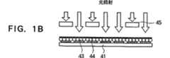
まず、図1Aに示すように、光硬化性樹脂をバインダ材44として用いて、マイクロカプセル43を、電極42が形成された基板41上に均一に塗布する。
【0016】
次に、図1Bに示すように、フォトマスク45を使用して、基板41のマイクロカプセル43を配置したい部分にのみ、選択的に光を照射し、バインダ材44を硬化させる。
そして、硬化させていない部分のバインダ材44を、水洗により除去する。
【0017】
その結果、図1Cに示すように、所望の位置にのみ選択的かつ正確に、マイクロカプセルを配置することができる。
このように、本実施の形態の表示パネルの製造方法においては、マイクロカプセルを配置したい箇所に光を照射するのみで、その所望の位置にマイクロカプセルを配置することができる。したがって、たとえばマイクロカプセルを基板41上に塗布する工程において特段の精細な位置制御などを必要とせず、マイクロカプセルを所望の位置に選択的かつ正確に、さらに非常に容易に配置することができる。
【0018】
第2の実施の形態
次に、本発明の第2の実施の形態として、各画素ごとにフルカラー表示の可能な電気泳動表示パネルの製造方法について、図2A〜図5Dを参照して説明する。
【0019】
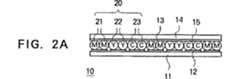
まず、その表示パネルの構成について説明する。
図2Aおよび図2Bは、その表示パネルの構成を示す図であり、図2Aは表示パネルの構造を示すための断面図、図2Bはマイクロカプセルの配列を模式的に示すための表示パネル上面図である。
【0020】
本実施の形態の表示パネル10は、図2Aに示すように、第1の電極12が形成された下面基板11と、第2の電極13形成された上面基板14とが、電極が対向するように配置され、さらにその間に、各々分散媒がマゼンダ(M),イエロー(Y),シアン(C)に着色された3種類のマイクロカプセル21,22,23が所定の配列で配置された構成である。
なお、表示パネル10は、第2の電極13および上面基板14側が表示面である。
【0021】
この3種類のマイクロカプセル21(M),22(Y),23(C)は、行方向および列方向に整然と配置された2次元配列であって、図2Bに示すような、行方向に同じ色が2列ずつ連続して順次繰り返され列方向に同じ色がつながったようなストライプ配列で、下面基板11上に配置される。
下面基板11は、表示パネル10を支持する任意の絶縁部材で構成された基板である。
【0022】
第1の電極12は、図2Bに示したように、行方向に連続して配置されている同じ色の2個ずつのマイクロカプセルの組の各々に対して、独立して所望の電界を印加可能なように形成された分割電極であり、下面基板11上に形成される。本実施の形態の表示パネル10の第1の電極12は、各マイクロカプセルの組に対応した電極ごとにスイッチ素子が設けられたものであり、これにより、図示せぬマトリクス駆動回路から行ごとに選択信号が印加され、さらに各列に制御信号と駆動トランジスタからの出力が印加されて、所望のマイクロカプセルの組に対して所望の電界が印加される。
【0023】
マイクロカプセル21,22,23は、各々、前述したような所定の色に着色された分散媒に、帯電された顔料粒子が混合・分散されて、マイクロカプセル中に収容されたものである。本実施の形態の表示パネル10は、減色混合により色を再現するものであり、前述したように、各分散媒は、シアン(C)、マゼンタ(M)およびイエロー(Y)の3種類に、また、帯電顔料粒子は白に、各々染色される。
【0024】
その3種類の各マイクロカプセルの構成を図3A〜図3Cに示す。
【0025】
図3Aは、マゼンタ(M)のマイクロカプセル21を示す図であり、マゼンタで染色された分散媒24中に白色顔料粒子27が分散している状態を示している。図3Bは、イエロー(Y)のマイクロカプセル22を示す図であり、イエローで染色された分散媒25中に白色顔料粒子27が分散している状態を示している。また、図3Cは、シアン(C)のマイクロカプセル23を示す図であり、シアンで染色された分散媒26中に白色顔料粒子27が分散している状態を示している。
【0026】
このようなマイクロカプセルに対して、外部から電界を印加した時の状態について、マゼンタのマイクロカプセル21を例にして図4Aおよび図4Bを参照して説明する。
いま、白色顔料粒子27が負に帯電されているものとし、マイクロカプセル21に対して、図4Aに示すような方向に電界Eが印加されたとすると、負に帯電している白色顔料粒子27は下側に泳動し、底面に集中して分布する。その結果、このマイクロカプセル21を上から見た時には、マゼンタで染色された分散媒24の色、すなわちマゼンタが観察される。
【0027】
一方、このマイクロカプセル21に対して、図4Bに示すような方向の電界Eを印加すると、白色顔料粒子27は上側に泳動して、上面に集中して分布することになり、このマイクロカプセル21を上から見た時には白色が観察される。
【0028】
このようなマイクロカプセルが、図示のごとく、下面基板11上に形成された第1の電極12の各分割された電極の上に配置され、マイクロカプセル層が形成される。なお、この時、各マイクロカプセルは、バインダ材15により、第1の電極12と第2の電極13間に固定される。
そして、第1の電極12により、各マイクロカプセルに印加される電界が制御され、各マイクロカプセルがその分散媒の色または白色を呈示する。
【0029】
また、表示パネル10においては、このようなマゼンタ(M)、イエロー(Y)、シアン(C)の各色のマイクロカプセル21,22,23を、図2Aおよび図2Bに示すように、行方向に2行ずつ順番に繰り返し並ぶように配置し、3種類のマイクロカプセル各2個ずつの連続した6個のマイクロカプセル21,22,23で、1画素の表示部20が構成されるものとみなして制御を行う。これにより、各画素あたり、フルカラーでの表示が可能となる。
【0030】
第2の電極13は、マイクロカプセルの層を挟んで、第1の電極12と対向するように、上面基板14上に形成された電極である。本実施の形態においては、第2の電極13は、図2Bに示すように2次元的に配列されたマイクロカプセルを、全面同一電位で覆うように形成された透明電極である。
【0031】
上面基板14は、表示パネル10の表示面側の基板である。上面基板14は、第2の電極13とともに透明部材で形成され、これにより、表示面である上面基板14側より表示パネル10を見た時に、マイクロカプセルの状態、すなわち、マイクロカプセルによる所望の絵柄のカラー表示の状態が観察できるようになっている。
【0032】
次に、このような構成の表示パネル10の製造方法について説明する。
【0033】
まず、マゼンタ、イエロー、シアンの3色の分散媒と、白色顔料粒子を用いて3種類の分散液を作成する。
【0034】
次に、それら3種類の分散液をそれぞれ内包する3種類のマイクロカプセルを作成する。
【0035】
次に、ふるい分け、比重分離法などの任意の方法により、作成したマイクロカプセルの径を揃える。
【0036】
次に、これら径の揃った3種類のマイクロカプセルを、図2Bに示したような配列で、隙間がないように、下面基板11上に形成された第1の電極12の各分割電極上に順に配置していく。
【0037】
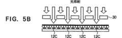
本発明に係わる、このマイクロカプセルの配置の方法について、図5A〜図5Dを参照して説明する。
【0038】
まず、図5Aに示すように、光硬化性樹脂をバインダ材15として用い、シアン(C)分散液内包のマイクロカプセル23を分割電極12が形成された下面基板11上に均一に塗布する。
【0039】
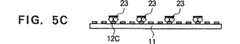
次に、図5Bに示すように、フォトマスク30を使用して、シアン(C)分散液内包のマイクロカプセル23を配置したい部分だけ、すなわち、シアンを発光色とする位置の電極12cだけに選択的に光を照射し、バインダ材15を硬化させる。
【0040】
そして、硬化させていない部分のバインダ材15を、水洗により除去する。
その結果、図5Cに示すように、シアンに対応する表示電極12c上だけに選択的かつ正確に、シアン(C)分散液内包のマイクロカプセル23を配置することができる。
【0041】
以後、同様の手順を繰り返し、順次イエロ−(Y)分散液内包のマイクロカプセル22およびマゼンタ(M)分散液内包のマイクロカプセル21を所定の位置に配置していく。
すなわち、まず、光硬化性樹脂をバインダ材15として用い、イエロ−(Y)分散液内包のマイクロカプセル22を分割電極12が形成された下面基板11上の、既にシアン(C)分散液内包のマイクロカプセル23が配置されていない箇所に塗布する。
【0042】
次に、フォトマスク30を使用して、イエロ−(Y)分散液内包のマイクロカプセル22を配置したい部分だけに選択的に光を照射し、バインダ材15を硬化させ、硬化させていない部分のバインダ材15を、水洗により除去する。
【0043】
最後に、光硬化性樹脂をバインダ材15として用い、マゼンタ(M)分散液内包のマイクロカプセル21を、分割電極12が形成された下面基板11上の、シアン(C)分散液内包のマイクロカプセル23およびイエロ−(Y)分散液内包のマイクロカプセル22が配置されていない箇所に塗布する。
そして、フォトマスク30を使用して、マゼンタ(M)分散液内包のマイクロカプセル21を配置したい部分だけに選択的に光を照射し、バインダ材15を硬化させる。
【0044】
その結果、図5Dに示すように、マゼンタ(M)、イエロー(Y)、シアン(C)の各分散液内包のマイクロカプセル21,22,23が、各々の色に対応する分割電極12m,12y,12c上に選択的かつ正確に配置される。
このようにして、第1の電極12の形成された下面基板11上にマイクロカプセル21,22,23を配置したら、このマイクロカプセル21,22,23を挟むように、第2の電極13を形成した上面基板14を張り合わせる。
【0045】
これにより、図2Aおよび図2Bに示したような構造の表示パネル10を製造することができる。
【0046】
以上説明したように、本実施の形態の表示パネルの製造方法においては、基板11一面に所望の色の分散液を内包したマイクロカプセルを塗布しておき、その色のマイクロカプセルを配置したい箇所に光を照射することで、その所望の位置に所望の色のマイクロカプセルを配置させるという工程を、マゼンタ(M)、イエロー(Y)、シアン(C)の各色ごとに行うことで、フルカラー表示可能な電気泳動表示パネルを製造している。したがって、特段の精細な位置制御などの工程を必要としない比較的容易な工程により、正確に各色のマイクロカプセルが配置された高精細なフルカラー電気泳動表示パネルを製造することができる。
【0047】
なお、本発明の表示パネルの製造方法は、前述した第1および第2の実施の形態に限られるものではなく、任意好適な種々の改変が可能である。
たとえば、第2の実施の形態においては、具体的な製造対象のパネルとして、フルカラー表示が可能な表示パネル10の製造方法を例示したが、本発明の表示パネルの製造方法は、モノクロ用表示パネルの製造に適用することができるのは明らかである。
【0048】
また、第1および第2の実施の形態においては、電気泳動方式の表示パネルを例示したが、磁気泳動方式の表示パネルも、これと同様の方式により構成することができる。その場合には、帯電顔料粒子を磁性粉にし、電圧印加手段を磁界印加手段に変更すればよい。
その際、表示パネルに具備されるべき磁界印加手段としては、通常知られている任意の手段を用いてよい。たとえば、磁気ヘッドや、種々の形態の磁石を用いてよい。
【0049】
また、第2の実施の形態においては、分散媒の色は、減色混合三原色である、マゼンタ、イエローおよびシアンの3種類としたが、加色混合三原色である、レッド、グリーンおよびブルーの3種類を用いてもよい。また、その他の任意の色の組み合わせを用いてよい。
【0050】
また、帯電顔料粒子の色は白であったが、たとえば分散媒の色に加色混合三原色を用いる際には、帯電顔料粒子の色を黒にするのが好適であり、そのようにしてもよい。帯電顔料粒子の色も、任意に決定してよい。
【0051】
また、第2の実施の形態においては、分散媒の色を変えることにより三原色に対応した3種類のマイクロカプセルを形成したが、分散媒の色は同じにし、マイクロカプセルの色を変えることにより、三原色に対応した3種類のマイクロカプセルを形成するようにしてもよい。
【0052】
また、第2の実施の形態において三原色の3種類のマイクロカプセルの2次元的配列は、図2Bに示すように、同じ色が2列ずつ連続して列方向につながるようなストライプ配列の場合を例示した。しかし、この3種類のマイクロカプセルの配置も、本実施の形態に限られるものではない。たとえば、マイクロカプセルは縦横に整然と配列しているものの、その種類が縦方向にも横方向にも順に変わるような、いわゆるモザイク配列にしてもよい。また、マイクロカプセル自体が行によって互い違いになるようないわゆる三角形配列にしてもよい。
【0053】
また、1画素の構成も、本実施の形態のように、一列に連なった6個のマイクロカプセルで規定してもよいし、たとえば、1列に連なった3個のマイクロカプセルや、いずれかの色のマイクロカプセルを2個有するような4個のマイクロカプセルを2×2に配置したような構成で規定してもよく任意に決定してよい。
【0054】
また、本発明に係わる表示パネルの製造方法においては、電極あるいは磁極に対応した形状のフォトマスクを用いることにより、マイクロカプセルを配置する領域を制御している。したがって、マイクロカプセルが電極に対して十分に小さければ、前述した第1および第2の実施の形態のようにマイクロカプセルを整然と並べて配置する必要はない。マイクロカプセルをなるべく均一な層となるように塗布し、電極の形状あるいは画素形状に対応したフォトマスクを用いて固定するマイクロカプセルを選択するようにすればよい。そのような方法も本発明の範囲内である。
【0055】
以上説明したように、本発明によれば、マイクロカプセルを所望の位置に選択的かつ正確に配置することができる、電気泳動または磁気泳動を用いた表示パネルの製造方法を提供することができる。また、これにより、高精細な表示あるいはフルカラー表示が可能な電気泳動または磁気泳動を用いた表示パネルの製造方法を提供することができる。さらに、マイクロカプセルが所望の位置に選択的かつ正確に配置された電気泳動または磁気泳動を用いた表示パネルを提供することができる。
【図面の簡単な説明】
【図1】図1A〜図1Cは、本発明の第1の実施の形態の表示パネルの製造方法を説明するための図であり、図1Aは、マイクロカプセルを基板上に塗布した状態を示す図であり、図1Bは、マイクロカプセルを配置したい所望の位置に光を照射する工程を示す図であり、図1Cは、マイクロカプセルを配置したくない箇所に塗布したマイクロカプセルを水洗して除去した状態を示す図である。
【図2】図2Aおよび図2Bは、本発明の第2の実施の形態の表示パネルの構成を示す図であり、図2Aは、表示パネルの構造を示すための断面図であり、図2Bは、マイクロカプセルの配列を模式的に示すための表示パネル上面図である。
【図3】図3A〜図3Cは、3種類のマイクロカプセルの構成を示す図であり、図3Aは、マゼンタ(M)の分散液を内包するマイクロカプセルを示す図であり、図3Bは、イエロー(Y)の分散液を内包するマイクロカプセルを示す図であり、図3Cは、シアン(C)の分散液を内包するマイクロカプセルを示す図である。
【図4】図4Aおよび図4Bは、図3Aに示したマゼンタ(M)の分散液を内包するマイクロカプセルに対して外部から電界を印加した時の状態を示す図であり、図4Aは、下から上方向に電界を印加した時のマイクロカプセルの内部状態を示す図であり、図4Bは、上から下方向に電界を印加した時のマイクロカプセルの内部状態を示す図である。
【図5】図5は、本発明の第2の実施の形態の表示パネルの製造方法を説明するための図であり、図5Aは、マイクロカプセルを基板上に塗布した状態を示す図であり、図5Bは、マイクロカプセルを配置したい所望の位置に光を照射する工程を示す図であり、図5Cは、マイクロカプセルを配置しない箇所に塗布したマイクロカプセルを水洗して除去した状態を示す図であり、図5Dは,図5A〜図5Cの工程を繰り返すことにより最終的に複数種類のマイクロカプセルが基板上に配置された状態を示す図である。
【符号の説明】
10…表示パネル、11…下面基板、12…第1の電極(分割電極)、13…第2の電極、14…上面基板、15…バインダ材、20…画素表示部、21…シアン(C)のマイクロカプセル、22…マゼンタ(M)のマイクロカプセル、23…イエロー(Y)のマイクロカプセル、24,25,26…分散媒、27…白色顔料粒子、30…フォトマスク、41…基板、42…電極、43…マイクロカプセル、44…バインダ材、45…フォトマスク[0001]
BACKGROUND OF THE INVENTION
The present invention relates to a display panel using microcapsules containing electrophoretic particles or magnetophoretic particles, and more particularly to a method of manufacturing a display panel capable of accurately arranging microcapsules at predetermined positions on electrodes.
[0002]
[Prior art]
In electrophoretic display devices and magnetophoretic display devices that use a microcapsule encapsulating colored dispersion medium and electrophoretic particles to display a desired pattern using electrophoresis or magnetophoresis, the microcapsules are evenly placed on the substrate. It is important to arrange them in a stable display operation.
As a method for uniformly applying such microcapsules on a flat surface, many methods for producing pressure-sensitive paper and thermal paper have been proposed.
[0003]
For example, Japanese Patent No. 1545227 discloses a method for producing pressure-sensitive copying paper by a free-falling vertical curtain method as a suitable method in place of the conventional air knife coating method and blade coating method.
Japanese Patent No. 1376224 discloses a hobber type coating apparatus as a similar method.
In Japanese Patent Application Laid-Open No. 57-27172, a microcapsule coating solution is sprayed onto a continuously running web (support) by spraying, and this is smoothed by a leveling device to obtain a continuous coating layer having a constant thickness. A method is disclosed.
[0004]
Furthermore, in Japanese Patent Laid-Open No. 62-138284, after forming an adhesive layer on a substrate, a microcapsule layer is formed thereon, and microcapsules that are not in contact with the adhesive layer are separated by gravity to form a single layer. A method for forming a uniform microcapsule layer is disclosed.
[0005]
However, all of the above-described methods are intended only for obtaining a uniform layer of microcapsules, and are not sufficient as a method for forming a microcapsule layer used for a display panel.
In a display panel, it is important to appropriately arrange microcapsules at positions corresponding to electrodes or magnetic poles constituting display pixels in order to display a high-definition image without unevenness for each pixel. Not only the formation of the capsule layer but also the control of the location of the individual microcapsules is required.
[0006]
In particular, when performing color display, it is necessary to arrange a plurality of microcapsules with different display colors for each pixel and to control them independently, in order to perform such control. For example, microcapsules of each display color must be selectively and accurately arranged on display electrodes patterned in segments on a substrate, and microcapsules must be arranged with higher accuracy. .
[0007]
In this respect, none of the above-described methods has presented a method for selectively and accurately arranging the microcapsules at a desired position, and there has been no such method so far.
[0008]
[Problems to be solved by the invention]
An object of the present invention is to provide a method for manufacturing a display panel using electrophoresis or magnetophoresis, in which microcapsules can be selectively and accurately arranged at desired positions.
Another object of the present invention is to provide an electrophoretic or magnetophoretic display panel capable of selectively and accurately arranging microcapsules at desired positions, thereby enabling high-definition display or full-color display. It is in providing the manufacturing method of.
[0009]
[Means for Solving the Problems]
According to the present invention, microcapsules each encapsulating a dispersion medium colored in a predetermined color and electrophoretic particles or magnetophoretic particles are arrangedcorresponding to each region defining one pixel, and theone pixel A method of manufacturing a display panel that displays an image by changing the display color of the microcapsule by applying an electric field or a magnetic field to the microcapsulein each of the regions defining
Amicrocapsule in which at least one dispersion medium colored in a predetermined color and electrophoretic particles or magnetophoretic particles are encapsulated in each of the regions defining the pixels on the substrate, and a photocurable resin as a binder material And using as a coating process,
A step of fixingeach prior Symbolmicrocapsules selectively irradiated with light so as to correspondto each region defining thepixel curing the binder material,to define a pixel on the substrate region ,
Removing the applied microcapsules and binder material other than the cured binder material and microcapsules fixed on the substrate;
A method of manufacturing a display panel having the above is provided.
[0010]
Preferably, the pretreatment step of applying microcapsules on the substrate, wherein a region defining one pixel, a plurality of first electrodes separated at a predetermined interval having a width definingthe pixel And a step of forming a second electrode facing the first electrode with the microcapsule sandwiched after the process of removing the applied microcapsule and binder material. .
[0011]
Preferably, in the step of fixing the microcapsule on the first electrode, light is selectively irradiated to correspond to each position of the first electrode using a photomask.
[0012]
Preferably, a microcapsule encapsulating a dispersion medium colored in any one of the three primary colors and electrophoretic or magnetophoretic particles colored in a predetermined color different from the three primary colors, For the three types of microcapsules distinguished by color, the process of each step is sequentially performed, and the three types of microcapsules are arranged on the substrate in a predetermined arrangement that defines theone pixel , so that color display is possible. Manufacture panels.
[0013]
Also preferably, a microcapsule encapsulating electrophoretic particles or magnetophoretic particles colored in any one of the three primary colors and a dispersion medium colored in a predetermined color different from the three primary colors, For the three types of microcapsules distinguished by the colors of the electrophoretic particles or the magnetophoretic particles, the processes of the respective steps are sequentially performed, and the three types of microcapsules are arranged on the substrate in a predetermined arrangement that defines theone pixel. A display panel that can be arranged and displayed in color is manufactured.
[0014]
DETAILED DESCRIPTION OF THE INVENTION
FirstEmbodiment First, as a first embodiment of the present invention, a basic display panel manufacturing method of the present invention, in which microcapsules are selectively and accurately arranged at arbitrary positions on a substrate. The method to do is demonstrated with reference to FIG. 1A-FIG. 1C.
1A to 1C are diagrams showing a process of arranging microcapsules at desired positions on a substrate.
[0015]
First, as shown in FIG. 1A,
[0016]
Next, as shown in FIG. 1B, using a
Then, the uncured portion of the
[0017]
As a result, as shown in FIG. 1C, the microcapsules can be selectively and accurately arranged only at a desired position.
As described above, in the display panel manufacturing method of the present embodiment, the microcapsules can be arranged at the desired positions only by irradiating light to the place where the microcapsules are to be arranged. Therefore, for example, in the process of applying the microcapsules on the
[0018]
SecondEmbodiment Next, as a second embodiment of the present invention, a method for manufacturing an electrophoretic display panel capable of full color display for each pixel will be described with reference to FIGS. 2A to 5D.
[0019]
First, the configuration of the display panel will be described.
2A and 2B are diagrams showing the configuration of the display panel, FIG. 2A is a cross-sectional view for showing the structure of the display panel, and FIG. 2B is a top view of the display panel for schematically showing the arrangement of the microcapsules. It is.
[0020]
In the
In the
[0021]
These three types of microcapsules 21 (M), 22 (Y), and 23 (C) are two-dimensional arrays arranged in an orderly manner in the row direction and the column direction, and are the same in the row direction as shown in FIG. 2B. The colors are arranged on the lower substrate 11 in a stripe arrangement in which the colors are successively repeated every two rows and the same color is connected in the row direction.
The bottom substrate 11 is a substrate made of an arbitrary insulating member that supports the
[0022]
As shown in FIG. 2B, the
[0023]
Each of the
[0024]
The structures of the three types of microcapsules are shown in FIGS. 3A to 3C.
[0025]
FIG. 3A is a diagram showing a magenta (M)
[0026]
A state when an electric field is applied from the outside to such a microcapsule will be described with reference to FIG. 4A and FIG. 4B by taking a
Now, assuming that the
[0027]
On the other hand, when an electric field E having a direction as shown in FIG. 4B is applied to the
[0028]
Such a microcapsule is arranged on each divided electrode of the
The electric field applied to each microcapsule is controlled by the
[0029]
Further, in the
[0030]
The
[0031]
The
[0032]
Next, a method for manufacturing the
[0033]
First, three types of dispersion liquids are prepared by using three color dispersion media of magenta, yellow, and cyan and white pigment particles.
[0034]
Next, three types of microcapsules each containing these three types of dispersions are prepared.
[0035]
Next, the diameters of the prepared microcapsules are made uniform by an arbitrary method such as sieving or specific gravity separation.
[0036]
Next, these three types of microcapsules having the same diameter are arranged on each divided electrode of the
[0037]
The method for arranging the microcapsules according to the present invention will be described with reference to FIGS. 5A to 5D.
[0038]
First, as shown in FIG. 5A, a
[0039]
Next, as shown in FIG. 5B, using the
[0040]
Then, the uncured portion of the
As a result, as shown in FIG. 5C, the
[0041]
Thereafter, the same procedure is repeated, and the
That is, first, the photocurable resin is used as the
[0042]
Next, the
[0043]
Finally, a photocurable resin is used as the
Then, using the
[0044]
As a result, as shown in FIG. 5D, the
When the
[0045]
Thereby, the
[0046]
As described above, in the display panel manufacturing method of the present embodiment, a microcapsule containing a dispersion liquid of a desired color is applied to the entire surface of the substrate 11, and the microcapsules of that color are to be disposed. Full color display is possible by performing the process of arranging microcapsules of the desired color at the desired position by irradiating light for each color of magenta (M), yellow (Y), and cyan (C) Manufacturing electrophoretic display panels. Therefore, a high-definition full-color electrophoretic display panel in which the microcapsules of each color are accurately arranged can be manufactured by a relatively easy process that does not require a special fine position control process.
[0047]
The method for manufacturing a display panel according to the present invention is not limited to the first and second embodiments described above, and various suitable modifications can be made.
For example, in the second embodiment, the manufacturing method of the
[0048]
In the first and second embodiments, the electrophoretic display panel is exemplified, but the magnetophoretic display panel can also be configured in the same manner. In that case, the charged pigment particles may be made of magnetic powder, and the voltage applying means may be changed to magnetic field applying means.
At that time, any conventionally known means may be used as the magnetic field applying means to be provided in the display panel. For example, a magnetic head or various types of magnets may be used.
[0049]
In the second embodiment, the three colors of the dispersion medium are magenta, yellow, and cyan, which are subtractive mixed three primary colors. However, three types of colors, red, green, and blue, which are additive mixed mixed primary colors. May be used. Also, any other color combination may be used.
[0050]
Further, although the color of the charged pigment particles was white, for example, when the additive mixed three primary colors are used for the color of the dispersion medium, it is preferable to set the color of the charged pigment particles to black. Good. The color of the charged pigment particles may be arbitrarily determined.
[0051]
In the second embodiment, three types of microcapsules corresponding to the three primary colors are formed by changing the color of the dispersion medium. However, by changing the color of the microcapsules by using the same dispersion medium color, Three types of microcapsules corresponding to the three primary colors may be formed.
[0052]
In the second embodiment, the two-dimensional arrangement of the three types of microcapsules of the three primary colors is a stripe arrangement in which the same color is continuously connected in the column direction by two columns as shown in FIG. 2B. Illustrated. However, the arrangement of these three types of microcapsules is not limited to the present embodiment. For example, although the microcapsules are regularly arranged in the vertical and horizontal directions, a so-called mosaic arrangement may be employed in which the types change in order in the vertical and horizontal directions. Also, a so-called triangular arrangement may be employed in which the microcapsules themselves are staggered depending on the rows.
[0053]
Further, the configuration of one pixel may be defined by six microcapsules arranged in a row as in the present embodiment, for example, three microcapsules arranged in a row, It may be defined by a configuration in which four microcapsules having two color microcapsules are arranged in 2 × 2 or may be arbitrarily determined.
[0054]
In the display panel manufacturing method according to the present invention, the region where the microcapsules are arranged is controlled by using a photomask having a shape corresponding to the electrode or the magnetic pole. Therefore, if the microcapsules are sufficiently small with respect to the electrodes, it is not necessary to arrange the microcapsules in an orderly manner as in the first and second embodiments described above. The microcapsules may be applied in a uniform layer as much as possible, and the microcapsules to be fixed may be selected using a photomask corresponding to the electrode shape or pixel shape. Such a method is also within the scope of the present invention.
[0055]
As described above, according to the present invention, it is possible to provide a method for manufacturing a display panel using electrophoresis or magnetophoresis, in which microcapsules can be selectively and accurately arranged at desired positions. Accordingly, it is possible to provide a method for manufacturing a display panel using electrophoresis or magnetophoresis capable of high-definition display or full-color display. Furthermore, a display panel using electrophoresis or magnetophoresis in which microcapsules are selectively and accurately arranged at desired positions can be provided.
[Brief description of the drawings]
FIG. 1A to FIG. 1C are views for explaining a method of manufacturing a display panel according to a first embodiment of the present invention, and FIG. 1A shows a state where microcapsules are applied on a substrate. FIG. 1B is a diagram showing a process of irradiating light to a desired position where a microcapsule is to be arranged, and FIG. 1C is a step of rinsing and removing a microcapsule applied to a place where a microcapsule is not desired It is a figure which shows the state which carried out.
2A and 2B are diagrams illustrating a configuration of a display panel according to a second embodiment of the present invention, and FIG. 2A is a cross-sectional view illustrating the structure of the display panel, and FIG. These are top views of a display panel for schematically showing the arrangement of microcapsules.
FIGS. 3A to 3C are diagrams showing configurations of three types of microcapsules, FIG. 3A is a diagram showing microcapsules enclosing a magenta (M) dispersion, and FIG. FIG. 3C is a diagram showing a microcapsule containing a yellow (Y) dispersion, and FIG. 3C is a diagram showing a microcapsule containing a cyan (C) dispersion.
4A and FIG. 4B are diagrams showing a state when an electric field is applied from the outside to the microcapsules enclosing the magenta (M) dispersion shown in FIG. 3A, and FIG. FIG. 4B is a diagram illustrating the internal state of the microcapsule when an electric field is applied from the bottom to the top, and FIG. 4B is a diagram illustrating the internal state of the microcapsule when the electric field is applied from the top to the bottom.
FIG. 5 is a diagram for explaining a method for manufacturing a display panel according to a second embodiment of the present invention, and FIG. 5A is a diagram showing a state in which microcapsules are applied on a substrate; FIG. 5B is a diagram showing a process of irradiating light to a desired position where a microcapsule is to be arranged, and FIG. FIG. 5D is a diagram showing a state in which a plurality of types of microcapsules are finally arranged on the substrate by repeating the processes of FIGS. 5A to 5C.
[Explanation of symbols]
DESCRIPTION OF
Claims (5)
Translated fromJapanese基板上の前記画素を規定する領域のそれぞれに、少なくとも1つの各々所定の色に着色された分散媒と電気泳動粒子または磁気泳動粒子とが封入されたマイクロカプセルを、光硬化性樹脂をバインダ材として用いて、塗布する工程と、
前記1画素を規定する領域のそれぞれに対応させて選択的に光を照射して前記バインダ材を硬化させ、前記基板上の1画素を規定する領域のそれぞれに前記マイクロカプセルを固着させる工程と、
前記硬化されたバインダ材および前記基板上に固着されたマイクロカプセル以外の、前記塗布されたマイクロカプセルおよびバインダ材を除去する工程と、
を有する表示パネルの製造方法。Microcapsuleseach enclosing a dispersion medium colored in a predetermined color and electrophoretic particles or magnetophoretic particles are arranged incorrespondence with each ofthe regions defining one pixel, and each of the regions defining the one pixel A method of manufacturing a display panel that displays an image by changing the display color of the microcapsule by applying an electric field or a magnetic field to the microcapsule in
Amicrocapsule in which at least one dispersion medium colored in a predetermined color and electrophoretic particles or magnetophoretic particles are encapsulated in each of the regions defining the pixels on the substrate, and a photocurable resin as a binder material And using as a coating process,
A step of fixingeach prior Symbolmicrocapsules selectively irradiated with light so as to correspondto each region defining thepixel curing the binder material,to define a pixel on the substrate region ,
Removing the applied microcapsules and binder material other than the cured binder material and microcapsules fixed on the substrate;
A method of manufacturing a display panel having
前記塗布されたマイクロカプセルおよびバインダ材を除去する工程の処理の後に、前記マイクロカプセルを挟んで前記第1の電極と対向する第2の電極を形成する工程と
をさらに有する、
請求項1に記載の表示パネルの製造方法。A pretreatment step of applying microcapsules on the substrate, as an area for defining the pixel, to form a plurality of first electrodes separated at a predetermined interval having a width definingthe pixel Process,
After the process of removing the applied microcapsule and binder material, further comprising the step of forming a second electrode facing the first electrode across the microcapsule,
The manufacturing method of the display panel of Claim 1.
請求項2に記載の表示パネルの製造方法。In the step of fixing the microcapsule on the first electrode, light is selectively irradiated in correspondence with each position of the first electrode using a photomask.
The manufacturing method of the display panel of Claim 2.
請求項1〜3のいずれかに記載の表示パネルの製造方法。A microcapsule in which a dispersion medium colored in any one of the three primary colors and electrophoretic or magnetophoretic particles colored in a predetermined color different from the three primary colors are enclosed, and is distinguished by the color of the dispersion medium The three types of microcapsules are sequentially processed in the above steps, and the three types of microcapsules are arranged on the substrate in a predetermined arrangement that defines theone pixel to produce a display panel capable of color display.to,
The manufacturing method of the display panel in any one of Claims 1-3.
請求項1〜4のいずれかに記載の表示パネルの製造方法。A microcapsule in which electrophoretic particles or magnetophoretic particles colored in any one of the three primary colors and a dispersion medium colored in a predetermined color different from the three primary colors are encapsulated, the electrophoretic particles or For the three types of microcapsules distinguished by the color of the magnetophoretic particles, the process of each step is sequentially performed, and the three types of microcapsules are arranged on the substrate in a predetermined arrangement that defines theone pixel. Manufacturing display panels,
The manufacturing method of the display panel in any one of Claims 1-4.
Applications Claiming Priority (2)
| Application Number | Priority Date | Filing Date | Title |
|---|---|---|---|
| JP4163799 | 1999-02-19 | ||
| PCT/JP2000/000976WO2000049593A1 (en) | 1999-02-19 | 2000-02-21 | Method for producing display panel and display panel |
Publications (1)
| Publication Number | Publication Date |
|---|---|
| JP4026317B2true JP4026317B2 (en) | 2007-12-26 |
Family
ID=12613855
Family Applications (1)
| Application Number | Title | Priority Date | Filing Date |
|---|---|---|---|
| JP2000600256AExpired - Fee RelatedJP4026317B2 (en) | 1999-02-19 | 2000-02-21 | Manufacturing method of display panel |
Country Status (4)
| Country | Link |
|---|---|
| US (4) | US6583780B1 (en) |
| JP (1) | JP4026317B2 (en) |
| AU (1) | AU2575700A (en) |
| WO (1) | WO2000049593A1 (en) |
Families Citing this family (23)
| Publication number | Priority date | Publication date | Assignee | Title |
|---|---|---|---|---|
| US7167155B1 (en) | 1995-07-20 | 2007-01-23 | E Ink Corporation | Color electrophoretic displays |
| US7075502B1 (en) | 1998-04-10 | 2006-07-11 | E Ink Corporation | Full color reflective display with multichromatic sub-pixels |
| AU2575700A (en)* | 1999-02-19 | 2000-09-04 | Nok Corporation | Method for producing display panel and display panel |
| US7408696B2 (en)* | 2000-03-03 | 2008-08-05 | Sipix Imaging, Inc. | Three-dimensional electrophoretic displays |
| CN1237623C (en) | 2000-04-18 | 2006-01-18 | 伊英克公司 | Method for forming transistor on substrate and substrate containing polyphenylene polyimide |
| US7893435B2 (en) | 2000-04-18 | 2011-02-22 | E Ink Corporation | Flexible electronic circuits and displays including a backplane comprising a patterned metal foil having a plurality of apertures extending therethrough |
| JP4797282B2 (en)* | 2001-06-06 | 2011-10-19 | 凸版印刷株式会社 | Manufacturing method of display panel |
| US20030193726A1 (en)* | 2002-04-16 | 2003-10-16 | Davidson Mark Peter | Active reflection illumination and projection |
| JP4416380B2 (en)* | 2002-06-14 | 2010-02-17 | キヤノン株式会社 | Electrophoretic display device and driving method thereof |
| JP2004271610A (en)* | 2003-03-05 | 2004-09-30 | Canon Inc | Color electrophoretic display |
| JP2004268438A (en)* | 2003-03-10 | 2004-09-30 | Konica Minolta Holdings Inc | Recording material and image forming method |
| JP2004295025A (en)* | 2003-03-28 | 2004-10-21 | Konica Minolta Holdings Inc | Recording material and image forming method |
| US7206119B2 (en)* | 2003-12-31 | 2007-04-17 | E Ink Corporation | Electro-optic displays, and method for driving same |
| JP4513414B2 (en)* | 2004-05-11 | 2010-07-28 | 富士ゼロックス株式会社 | Image display device |
| JP4579768B2 (en)* | 2004-06-02 | 2010-11-10 | セイコーエプソン株式会社 | Method for producing electrophoretic display sheet, electrophoretic display sheet and use thereof |
| JP2008155067A (en)* | 2005-04-14 | 2008-07-10 | Toray Eng Co Ltd | Method and apparatus for manufacturing microcapsule and microcapsule sheet |
| US7952790B2 (en) | 2006-03-22 | 2011-05-31 | E Ink Corporation | Electro-optic media produced using ink jet printing |
| US8077142B2 (en)* | 2006-09-27 | 2011-12-13 | Tred Displays Corporation | Reflective, bi-stable magneto optical display architectures |
| JP5028970B2 (en)* | 2006-11-22 | 2012-09-19 | 凸版印刷株式会社 | Multicolor display panel manufacturing method and multicolor display panel image display method |
| US9104082B2 (en)* | 2011-06-29 | 2015-08-11 | Hewlett-Packard Development Company, L.P. | Electronic paper with porous standoff layer |
| CN102629064B (en) | 2011-11-21 | 2015-03-25 | 京东方科技集团股份有限公司 | Methods for preparing color microcapsule membrane material and display device comprising membrane material |
| WO2020132362A1 (en) | 2018-12-21 | 2020-06-25 | E Ink Corporation | Sub-threshold addressing and erasing in a magneto-electrophoretic writing medium |
| CN114174961B (en) | 2019-08-08 | 2022-10-21 | 伊英克公司 | Stylus for addressing magnetically driven display media |
Family Cites Families (29)
| Publication number | Priority date | Publication date | Assignee | Title |
|---|---|---|---|---|
| GB1458045A (en)* | 1973-08-15 | 1976-12-08 | Secr Defence | Display systems |
| US4045327A (en)* | 1974-08-28 | 1977-08-30 | Matsushita Electric Industrial Co., Ltd. | Electrophoretic matrix panel |
| US4041481A (en)* | 1974-10-05 | 1977-08-09 | Matsushita Electric Industrial Co., Ltd. | Scanning apparatus for an electrophoretic matrix display panel |
| US4508807A (en)* | 1983-07-11 | 1985-04-02 | Mead Corporation | Photosensitive material employing encapsulated radiation sensitive composition and a transparentizable image-receiving layer |
| US4696885A (en)* | 1983-09-06 | 1987-09-29 | Energy Conversion Devices, Inc. | Method of forming a large surface area integrated circuit |
| JP2551783B2 (en) | 1987-09-29 | 1996-11-06 | エヌオーケー株式会社 | Electrophoretic display device |
| JP3184212B2 (en) | 1990-11-29 | 2001-07-09 | 株式会社リコー | Color display panel, color display device, and color display method using the same |
| JP3089612B2 (en) | 1993-04-08 | 2000-09-18 | 松下電器産業株式会社 | Color filter |
| US5559615A (en) | 1993-10-07 | 1996-09-24 | Casio Computer Co., Ltd. | Polymer dispersed liquid crystal display device |
| JPH07104257A (en)* | 1993-10-07 | 1995-04-21 | Casio Comput Co Ltd | Polymer dispersed liquid crystal display device |
| JPH07110466A (en)* | 1993-10-14 | 1995-04-25 | Casio Comput Co Ltd | Polymer dispersed liquid crystal display device |
| JP3533471B2 (en)* | 1993-10-14 | 2004-05-31 | カシオ計算機株式会社 | Polymer dispersed liquid crystal display device |
| US5699097A (en)* | 1994-04-22 | 1997-12-16 | Kabushiki Kaisha Toshiba | Display medium and method for display therewith |
| JPH08179284A (en)* | 1994-12-21 | 1996-07-12 | Matsushita Electric Ind Co Ltd | Liquid crystal panel, method of manufacturing liquid crystal panel, and projection apparatus |
| US6459418B1 (en)* | 1995-07-20 | 2002-10-01 | E Ink Corporation | Displays combining active and non-active inks |
| JPH09160511A (en)* | 1995-12-11 | 1997-06-20 | Toppan Printing Co Ltd | Magnetic recording body and recording method thereof |
| US5717283A (en)* | 1996-01-03 | 1998-02-10 | Xerox Corporation | Display sheet with a plurality of hourglass shaped capsules containing marking means responsive to external fields |
| JPH09281908A (en) | 1996-04-17 | 1997-10-31 | Brother Ind Ltd | Display device |
| US5961804A (en)* | 1997-03-18 | 1999-10-05 | Massachusetts Institute Of Technology | Microencapsulated electrophoretic display |
| US5866284A (en)* | 1997-05-28 | 1999-02-02 | Hewlett-Packard Company | Print method and apparatus for re-writable medium |
| JP2841294B1 (en) | 1997-07-07 | 1998-12-24 | ケミテック株式会社 | Microcapsule magnetic display sheet and method of manufacturing the same |
| US6067185A (en)* | 1997-08-28 | 2000-05-23 | E Ink Corporation | Process for creating an encapsulated electrophoretic display |
| AU3767899A (en)* | 1998-04-27 | 1999-11-16 | E-Ink Corporation | Shutter mode microencapsulated electrophoretic display |
| WO1999059101A2 (en)* | 1998-05-12 | 1999-11-18 | E-Ink Corporation | Microencapsulated electrophoretic electrostatically-addressed media for drawing device applications |
| JP2000098597A (en)* | 1998-07-23 | 2000-04-07 | Matsushita Electric Ind Co Ltd | Resin thin film and method of manufacturing the same |
| JP2000137250A (en)* | 1998-11-04 | 2000-05-16 | Sony Corp | Display device and method for driving the display device |
| AU2575700A (en)* | 1999-02-19 | 2000-09-04 | Nok Corporation | Method for producing display panel and display panel |
| JP2001056653A (en)* | 1999-06-11 | 2001-02-27 | Ricoh Co Ltd | Display liquid for electrophoretic display, display particles, and display medium, display device, display method, display card, recording sheet, display, reversible display signboard using them |
| US6772798B2 (en)* | 2001-05-25 | 2004-08-10 | Illinois Tool Works, Inc. | Strapping tool |
- 2000
- 2000-02-21AUAU25757/00Apatent/AU2575700A/ennot_activeAbandoned
- 2000-02-21WOPCT/JP2000/000976patent/WO2000049593A1/enactiveApplication Filing
- 2000-02-21USUS09/673,372patent/US6583780B1/ennot_activeExpired - Lifetime
- 2000-02-21JPJP2000600256Apatent/JP4026317B2/ennot_activeExpired - Fee Related
- 2003
- 2003-05-09USUS10/434,240patent/US7199781B2/ennot_activeExpired - Lifetime
- 2006
- 2006-06-07USUS11/448,057patent/US7632163B2/ennot_activeExpired - Fee Related
- 2009
- 2009-11-02USUS12/588,923patent/US8169142B2/ennot_activeExpired - Fee Related
Also Published As
| Publication number | Publication date |
|---|---|
| US20030193473A1 (en) | 2003-10-16 |
| US6583780B1 (en) | 2003-06-24 |
| US20060228976A1 (en) | 2006-10-12 |
| AU2575700A (en) | 2000-09-04 |
| US20100046063A1 (en) | 2010-02-25 |
| WO2000049593A1 (en) | 2000-08-24 |
| US7632163B2 (en) | 2009-12-15 |
| US8169142B2 (en) | 2012-05-01 |
| US7199781B2 (en) | 2007-04-03 |
Similar Documents
| Publication | Publication Date | Title |
|---|---|---|
| JP4026317B2 (en) | Manufacturing method of display panel | |
| US6958842B2 (en) | Display device and process for production thereof | |
| JP2005500571A5 (en) | ||
| KR20110031326A (en) | Appearance-modifying devices, methods of making such devices and methods of operating such devices | |
| JP2000035598A (en) | Display panel | |
| WO2019161642A1 (en) | Color display device | |
| JP2004004282A (en) | Manufacturing method of electrophoretic display element | |
| JP3690124B2 (en) | Manufacturing method of display panel | |
| JP3842567B2 (en) | Electrophoretic display device | |
| CN114265256A (en) | Manufacturing method of electronic paper display equipment and electronic paper display equipment | |
| JP3868788B2 (en) | Electrophoretic display device | |
| JP4508322B2 (en) | Display device | |
| US8248362B1 (en) | Method of manufacturing an electrophoretic display | |
| JP3530117B2 (en) | Display device | |
| JPH07201466A (en) | Multicolor thin film electroluminescent device | |
| JPH04136916A (en) | Liquid crystal panel and production of liquid crystal panel | |
| US8436807B1 (en) | Single particle electrophoretic display and method of manufacturing same | |
| US8199305B2 (en) | Pixel well electrodes | |
| JP3721728B2 (en) | Sheet-shaped display medium, sheet-shaped display device, and method for manufacturing sheet-shaped display medium | |
| JP4113134B2 (en) | Display device | |
| JP3595729B2 (en) | Display device and method of manufacturing the same | |
| JP2003161822A (en) | Plastic color filter and display device using the same | |
| JP2659689B2 (en) | Manufacturing method of color filter | |
| JP5184186B2 (en) | Manufacturing method of color filter | |
| JP2005242233A (en) | Image display apparatus |
Legal Events
| Date | Code | Title | Description |
|---|---|---|---|
| A621 | Written request for application examination | Free format text:JAPANESE INTERMEDIATE CODE: A621 Effective date:20040301 | |
| A131 | Notification of reasons for refusal | Free format text:JAPANESE INTERMEDIATE CODE: A131 Effective date:20070313 | |
| A521 | Request for written amendment filed | Free format text:JAPANESE INTERMEDIATE CODE: A523 Effective date:20070514 | |
| A131 | Notification of reasons for refusal | Free format text:JAPANESE INTERMEDIATE CODE: A131 Effective date:20070626 | |
| A521 | Request for written amendment filed | Free format text:JAPANESE INTERMEDIATE CODE: A523 Effective date:20070827 | |
| TRDD | Decision of grant or rejection written | ||
| A01 | Written decision to grant a patent or to grant a registration (utility model) | Free format text:JAPANESE INTERMEDIATE CODE: A01 Effective date:20070918 | |
| A61 | First payment of annual fees (during grant procedure) | Free format text:JAPANESE INTERMEDIATE CODE: A61 Effective date:20071001 | |
| FPAY | Renewal fee payment (event date is renewal date of database) | Free format text:PAYMENT UNTIL: 20101019 Year of fee payment:3 | |
| R150 | Certificate of patent or registration of utility model | Free format text:JAPANESE INTERMEDIATE CODE: R150 | |
| FPAY | Renewal fee payment (event date is renewal date of database) | Free format text:PAYMENT UNTIL: 20101019 Year of fee payment:3 | |
| FPAY | Renewal fee payment (event date is renewal date of database) | Free format text:PAYMENT UNTIL: 20111019 Year of fee payment:4 | |
| FPAY | Renewal fee payment (event date is renewal date of database) | Free format text:PAYMENT UNTIL: 20121019 Year of fee payment:5 | |
| FPAY | Renewal fee payment (event date is renewal date of database) | Free format text:PAYMENT UNTIL: 20121019 Year of fee payment:5 | |
| FPAY | Renewal fee payment (event date is renewal date of database) | Free format text:PAYMENT UNTIL: 20131019 Year of fee payment:6 | |
| S531 | Written request for registration of change of domicile | Free format text:JAPANESE INTERMEDIATE CODE: R313531 | |
| R350 | Written notification of registration of transfer | Free format text:JAPANESE INTERMEDIATE CODE: R350 | |
| LAPS | Cancellation because of no payment of annual fees |