JP4024053B2 - High frequency plasma processing method and high frequency plasma processing apparatus - Google Patents
High frequency plasma processing method and high frequency plasma processing apparatusDownload PDFInfo
- Publication number
- JP4024053B2 JP4024053B2JP2002033167AJP2002033167AJP4024053B2JP 4024053 B2JP4024053 B2JP 4024053B2JP 2002033167 AJP2002033167 AJP 2002033167AJP 2002033167 AJP2002033167 AJP 2002033167AJP 4024053 B2JP4024053 B2JP 4024053B2
- Authority
- JP
- Japan
- Prior art keywords
- frequency
- plasma
- impedance matching
- frequency power
- plasma processing
- Prior art date
- Legal status (The legal status is an assumption and is not a legal conclusion. Google has not performed a legal analysis and makes no representation as to the accuracy of the status listed.)
- Expired - Fee Related
Links
Images


Classifications
- H—ELECTRICITY
- H01—ELECTRIC ELEMENTS
- H01J—ELECTRIC DISCHARGE TUBES OR DISCHARGE LAMPS
- H01J37/00—Discharge tubes with provision for introducing objects or material to be exposed to the discharge, e.g. for the purpose of examination or processing thereof
- H01J37/32—Gas-filled discharge tubes
- H01J37/32009—Arrangements for generation of plasma specially adapted for examination or treatment of objects, e.g. plasma sources
- H01J37/32082—Radio frequency generated discharge
- H—ELECTRICITY
- H05—ELECTRIC TECHNIQUES NOT OTHERWISE PROVIDED FOR
- H05H—PLASMA TECHNIQUE; PRODUCTION OF ACCELERATED ELECTRICALLY-CHARGED PARTICLES OR OF NEUTRONS; PRODUCTION OR ACCELERATION OF NEUTRAL MOLECULAR OR ATOMIC BEAMS
- H05H1/00—Generating plasma; Handling plasma
- H05H1/02—Arrangements for confining plasma by electric or magnetic fields; Arrangements for heating plasma
- H05H1/16—Arrangements for confining plasma by electric or magnetic fields; Arrangements for heating plasma using externally-applied electric and magnetic fields
- H05H1/18—Arrangements for confining plasma by electric or magnetic fields; Arrangements for heating plasma using externally-applied electric and magnetic fields wherein the fields oscillate at very high frequency, e.g. in the microwave range, e.g. using cyclotron resonance
- C—CHEMISTRY; METALLURGY
- C23—COATING METALLIC MATERIAL; COATING MATERIAL WITH METALLIC MATERIAL; CHEMICAL SURFACE TREATMENT; DIFFUSION TREATMENT OF METALLIC MATERIAL; COATING BY VACUUM EVAPORATION, BY SPUTTERING, BY ION IMPLANTATION OR BY CHEMICAL VAPOUR DEPOSITION, IN GENERAL; INHIBITING CORROSION OF METALLIC MATERIAL OR INCRUSTATION IN GENERAL
- C23C—COATING METALLIC MATERIAL; COATING MATERIAL WITH METALLIC MATERIAL; SURFACE TREATMENT OF METALLIC MATERIAL BY DIFFUSION INTO THE SURFACE, BY CHEMICAL CONVERSION OR SUBSTITUTION; COATING BY VACUUM EVAPORATION, BY SPUTTERING, BY ION IMPLANTATION OR BY CHEMICAL VAPOUR DEPOSITION, IN GENERAL
- C23C16/00—Chemical coating by decomposition of gaseous compounds, without leaving reaction products of surface material in the coating, i.e. chemical vapour deposition [CVD] processes
- C23C16/44—Chemical coating by decomposition of gaseous compounds, without leaving reaction products of surface material in the coating, i.e. chemical vapour deposition [CVD] processes characterised by the method of coating
- C23C16/50—Chemical coating by decomposition of gaseous compounds, without leaving reaction products of surface material in the coating, i.e. chemical vapour deposition [CVD] processes characterised by the method of coating using electric discharges
- C23C16/505—Chemical coating by decomposition of gaseous compounds, without leaving reaction products of surface material in the coating, i.e. chemical vapour deposition [CVD] processes characterised by the method of coating using electric discharges using radio frequency discharges
- H—ELECTRICITY
- H01—ELECTRIC ELEMENTS
- H01J—ELECTRIC DISCHARGE TUBES OR DISCHARGE LAMPS
- H01J37/00—Discharge tubes with provision for introducing objects or material to be exposed to the discharge, e.g. for the purpose of examination or processing thereof
- H01J37/32—Gas-filled discharge tubes
- H01J37/32009—Arrangements for generation of plasma specially adapted for examination or treatment of objects, e.g. plasma sources
- H01J37/32082—Radio frequency generated discharge
- H01J37/32137—Radio frequency generated discharge controlling of the discharge by modulation of energy
- H01J37/32155—Frequency modulation
- H01J37/32165—Plural frequencies
Landscapes
- Chemical & Material Sciences (AREA)
- Engineering & Computer Science (AREA)
- Physics & Mathematics (AREA)
- Plasma & Fusion (AREA)
- Analytical Chemistry (AREA)
- Organic Chemistry (AREA)
- General Chemical & Material Sciences (AREA)
- Chemical Kinetics & Catalysis (AREA)
- Materials Engineering (AREA)
- Mechanical Engineering (AREA)
- Metallurgy (AREA)
- Spectroscopy & Molecular Physics (AREA)
- Optics & Photonics (AREA)
- Plasma Technology (AREA)
- Physical Or Chemical Processes And Apparatus (AREA)
- Drying Of Semiconductors (AREA)
Description
Translated fromJapanese【0001】
【発明の属する技術分野】
本願の発明は、高周波エネルギーにより形成されたプラズマを利用した処理に関するものであり、特に、異なる二つの周波数の高周波を使用する処理に関するものである。
【従来の技術】
【0002】
高周波エネルギーにより形成されたプラズマを利用した処理(以下、単に高周波プラズマ処理)は、LSI(大規模集積回路)等の半導体デバイスやLCD(液晶ディスプレイ)等の表示デバイスの製造に盛んに利用されている。このような高周波プラズマ処理においては、VHF帯のような周波数のより高い高周波を使用することが多くなってきている。以下、この点について説明する。
高周波の周波数が高くなる一つの大きな要因は、プロセスの低圧化の要請である。プロセスの低圧化の要請は、デバイスの高集積度化や回路の微細化といった点と密接に関連している。回路がより微細化すると、僅かな異物(塵埃,パーティクル等)の混入によっても製品不良が発生する可能性が高い。従って、処理チャンバー内の圧力をより低くすることで、このような異物の混入を防止する必要がある。
【0003】
また、プロセスの低圧化は、より微細な加工を可能にする点からも重要な課題となっている。例えば、回路の微細化が進むと、コンタクトホールやビアホールのようなホールのアスペクト比は高くなる傾向にある。アスペクト比の高いホールを形成する技術として、プラズマ中のイオンを引き出して基板に入射させて利用するリアクティブイオンエッチング(RIE)が多用されている。イオン入射によって高アスペクト比のホール形成を行うためには、多くのイオンを基板に垂直な方向に加速して入射させることが重要である。しかしながら、圧力が高いと、イオンがガス分子に衝突してその方向を変えてしまうため、基板に斜めに入射し易い。この結果、ホールの側壁に多くイオンが入射して、いわゆる中膨れ形状(ボーイング形状)のホールとなってしまったりする問題がある。
【0004】
また、プラズマ中の気相反応を利用して薄膜を作成するプラズマ化学蒸着(CVD)では、圧力が高いと、プラズマ中で生成された活性種が衝突によって失活する可能性が高くなる。この結果、ダストと呼ばれる未反応生成物が多く残留し、処理チャンバー内の雰囲気を悪くする原因となり易い。また、成膜中の基板の表面からは、蒸気圧の低い副生成物が蒸発して放出されることがあるが、処理チャンバー内の圧力が高いと、それが再び基板に戻って残留し、薄膜の品質を損ねることがある。
【0005】
このようなことから、プロセスの低圧化の要請が顕著となってきている。一方、プロセスの低圧化とともに、生産性を向上させるためのプロセスの高速化の要請も依然として強い。プロセスの高速化のためには、一般的にはプラズマ密度(プラズマ中の荷電粒子の数密度)を高くすることが必要である。しかしながら、プロセスの高速化とプロセスの低圧化は、ある面では相反する要請である。つまり、低圧化すればするほど気体分子の数は少なくなるのであるから、プラズマ密度は低くならざるを得ない。
【0006】
圧力が低くなってもプラズマ密度を充分に高く維持するには、プラズマの形成効率を高めることが肝要になる。高周波プラズマ処理において、より高い周波数の高周波が使用されるようになってきている背景は、この点にある。具体的に説明すると、以前のプラズマ処理ではMF帯からHF帯の高周波がしばしば使用されたが、最近ではVHF帯の高周波が多く使用されるようになってきている。周波数が高くなると、電子が電界に追従して移動の向きを変える際の周期が短くなる。この結果、電子と中性ガス分子との衝突の頻度が高くなり、プラズマの形成効率が向上する。
【0007】
しかしながら、VHF帯のようなより高い周波数の高周波により形成したプラズマを利用して処理する場合、処理の品質や再現性を高く維持する観点から、別の問題が発生することがある。例えば、前述したRIEに見られるように、プラズマ処理ではプラズマ中からイオンを引き出して基板に入射させることがしばしば行われる。イオンの入射には、基板に向かって徐々に電位が下がる電界をプラズマと基板との間に設定する必要がある。この電界は、一般的にはプラズマが固体に接する際にその固体とプラズマとの間に現れるシース電界に相当している。基板をアースから絶縁することで基板を浮遊電位(floating potential)とすると、プラズマ電位(≒0V)を持つプラズマに対して負のシース電界を与えることができる。
【0008】
この負のシース電界により、プラズマ中からイオンを引き出して基板に入射させることができるのであるが、プラズマ形成用の高周波の周波数がVHF帯程度まで高くなってくると、シース電界が小さくなる問題がある。これは、あまりにも周波数が高くなるため、イオンのみならず電子についても電界の変化に追従することが難しくなるからである。基板を介して高周波を印加することで、基板に対して自己バイアス電圧を与えることで上記イオン入射を行うことも頻繁に行われるが、VHF帯程度まで周波数が高くなると、やはり電子が電界に追従して移動する量が少なくなるので、充分に大きな自己バイアス電圧が与えられなくなってしまう問題がある。
また、プラズマCVD等では、基板へのイオンの入射量や入射エネルギーが処理に影響を与えるため、それらを最適範囲に維持する必要がある。しかしながら、それとは別にプラズマを形成するための高周波の最適な印加条件があり、両者が両立しない場合も多い。
このような点を考慮し、最近では、プラズマ形成用としてVHF帯の高周波を印加し、VHF帯より周波数の低いHF帯の高周波を基板へのイオン入射用として別に印加する構成が採用されるようになってきている。
【0009】
【発明が解決しようとする課題】
しかしながら、本願の発明者の研究によると、VHF帯とHF帯のように、異なる二つの周波数の高周波を印加してプラズマを形成すると、プラズマへの高周波の結合が不充分になるためにプラズマが上手く維持でなかったり、プラズマが初期状態において不安定になる問題があることが判明した。
本願の発明は、このような課題を解決するために成されたものであり、二つの異なる周波数の高周波を使用してプラズマを形成する高周波プラズマ処理において、プラズマの形成や維持が充分に且つ安定して行えるようにし、それら二周波を利用するメリットを充分に享受できるようにするという技術的意義を有する。
【0010】
【課題を解決するための手段】
上記課題を解決するため、本願の請求項1記載の発明は、処理チャンバー内に基板を配置するとともに処理チャンバー内に高周波放電によるプラズマを形成して基板に所定の処理を施す高周波プラズマ処理方法であって、
第一の周波数の高周波電力を放電空間に供給して高周波放電を開始させる第一のステップと、
高周波放電を開始させた後、プラズマが形成されてプラズマが安定するのに必要な所定のタイムラグが経過してから、第一の周波数とは異なる第二の周波数の高周波電力を放電空間に供給する第二のステップとを有し、
前記第一のステップは、前記高周波放電の開始に適した第一のインピーダンス整合条件で高周波電力を供給して放電を開始させるものであり、その後、インピーダンス整合条件を、プラズマの安定化に適した第二のインピーダンス整合条件に変更する動作を含んでおり、
前記第二のインピーダンス整合条件は、プラズマが形成されている放電空間に結合する高周波電力の大きさが極大値となるか又は放電空間からの反射波が極小値となる条件であり、第二のステップは、放電空間への高周波電力の供給状況をモニタすることによりこの状態となるよう整合用インピーダンスの自動制御を行うステップであるという構成を有する。
上記課題を解決するため、請求項14記載の発明は、処理対象である基板が内部に配置される処理チャンバーと、処理チャンバー内にプロセスガスを導入するプロセスガス導入系と、処理チャンバー内に設けられた高周波電極と、高周波電極に高周波電圧を印加することで処理チャンバー内に高周波電界を設定して高周波放電を生じさせてプロセスガスのプラズマを形成する第一の高周波電源とを備え、プラズマを利用して基板に所定の処理を施す高周波プラズマ処理装置であって、
前記高周波電極又はこの高周波電極とは別に設けられた高周波電極に前記第一の高周波電源とは異なる周波数の高周波電圧を印加する第二の高周波電源が設けられており、
さらに、前記第一の高周波電源を動作させた後、プラズマが形成されてプラズマが安定化するのに必要な所定のタイムラグが経過してから、第二の高周波電源を動作させるシーケンス制御を行うコントローラが設けられており、
さらに、
前記第一の高周波電源と前記放電空間との間の高周波線路上にはプラズマ用整合器が設けられているとともに、このプラズマ用整合器を制御する整合器制御系が設けられており、前記コントローラは、前記高周波放電の開始に適した第一のインピーダンス整合条件で高周波電力の供給を開始して放電を開始させ、その後、インピーダンス整合条件を、プラズマの安定化に適した第二のインピーダンス整合条件に変更するよう整合器制御系を制御するものであり、
前記第二のインピーダンス整合条件は、放電空間に結合する高周波電力の大きさが極大値となるか又は放電空間からの反射波が極小値となる最適状態を達成する条件であり、放電空間への高周波電力の供給状況をモニタする電力供給状況モニタ手段が設けられており、前記整合器制御系は、電力供給状況モニタ手段からの信号により前記最適状態となるよう自動制御を行うものであるという構成を有する。
【0011】
【発明の実施の形態】
以下、本願発明の実施の形態(以下、実施形態)について説明する。
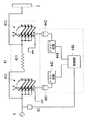
図1は、第一の実施形態に係る高周波プラズマ処理装置の正面断面概略図である。図1に示す装置は、排気系11を備えた処理チャンバー1と、処理チャンバー1内にプロセスガスを導入するプロセスガス導入系2と、導入されたプロセスガスに高周波放電を生じさせて処理チャンバー1内にプラズマを形成するプラズマ形成手段と、形成されたプラズマによって処理される位置に基板9を保持する基板ホルダー5とを備えている。
【0012】
プラズマ形成手段は、処理チャンバー1内に設けられた高周波電極3と、高周波電極3に高周波電圧を印加してプラズマを形成する高周波電源(以下、プラズマ用電源)4とから成っている。さらに、プラズマからイオンを引き出して基板9に入射させるための高周波電源(以下、イオン入射用電源)50が、プラズマ用高周波電源4とは別に設けられている。イオン入射用高周波電源50は、基板ホルダー5に接続されている。
【0013】
処理チャンバー1は気密な真空容器であり、不図示のゲートバルブを介して不図示のロードロックチャンバーが接続されている。排気系11は、ターボ分子ポンプ又は拡散ポンプ等により処理チャンバー1内を所定の真空圧力まで排気できるようになっている。
図1に示す装置は、エッチングを行う装置となっている。具体的には、プロセスガス導入系2は、フッ素系ガス等のエッチング作用のあるガスを導入するようになっている。プロセスガス導入系2は、バルブ21や流量調整器22を備え、プロセスガスを所定の流量で導入するようになっている。
高周波電極3は、基板ホルダー5に平行に対向させた円盤状である。高周波電極3は、絶縁材31を介して処理チャンバー1の上壁部の開口に気密に取り付けられている。
【0014】
プラズマ用電源4は、プラズマ用整合器41を介して高周波電極3に接続されている。プラズマ用整合器41から高周波電極3への伝送路には、図1に示すように同軸管42が使用されている。同軸管42は、内導体421と、内導体421と同軸の円筒状の外導体422とから成る。尚、同軸管42は、高周波電極3と同軸である。
【0015】
基板ホルダー5は、上面に基板9を載置して保持するものである。基板9の保持位置は、基板9が高周波電極3と同軸になる位置である。尚、基板9は薄い円形状であり、高周波電極3や基板ホルダー5も同軸の円盤状である。
また、基板ホルダー5は、基板9を静電吸着して保持するようになっている。即ち、図1には明示していないが、基板ホルダー5は、上側が誘電体製であり、その誘電体製の部分の内部に不図示の吸着電極が埋設されている。そして、吸着電極に静電吸着用の直流電圧を印加する不図示の吸着電源が設けられている。吸着電源が電圧を印加すると、基板ホルダー5の上面に静電気が誘起され、基板9が静電吸着されるようになっている。
この基板ホルダー5は、高周波電極3とともに放電空間を形成する別の高周波電極になっている。基板ホルダー5は、高周波電極3と同軸上に配置されて対向している。つまり、基板ホルダー5と高周波電極3とは、平行平板電極を構成している。
【0016】
処理チャンバー1の下側には、同軸の円筒部62が設けられている。円筒部62は底板部を有し、その中央部分で接地されている。従って、処理チャンバー1は、直流的には接地電位である。基板ホルダー5は、処理チャンバー1から絶縁材52によって絶縁されている。従って、基板ホルダー5は、直流的には接地電位から浮いた状態、つまり浮遊電位を取るようになっている。
また、基板ホルダー5は、同軸に設けられた支柱61によって支えられている。円筒部62、支柱61、基板ホルダー5、処理チャンバー1等は、すべて同軸である。イオン入射用電源50は、支柱61を介して基板ホルダー5に接続されている。尚、円筒部62には、イオン入射用整合器51が設けられており、イオン入射用電源50は、イオン入射用整合器51を介して基板ホルダー5に高周波電圧を印加するようになっている。
【0017】
基板ホルダー5の周囲を取り囲むようにして、シールド12が設けられている。シールド12も、基板ホルダー5等と同様に、基板9と同軸であり、円筒形である。シールド12は、処理チャンバー1の底壁部に下端が固定されている。シールド12は、基板ホルダー5の周囲で放電が生ずるのを防止するものである。尚、基板ホルダー5、シールド12、処理チャンバー1の底板部、円筒部62、支柱61等が、プラズマ用電源4の周波数で共振するよう構成されていると、基板ホルダー5が高周波的に接地された状態となり、高周波電極3と基板ホルダー5との間の電圧が最も高くなって高周波放電が最も効率よくなるので、効果的である。
【0018】
さて、本実施形態の装置は、前述したような二周波タイプの装置となっている。即ち、プラズマ用電源4は、本実施形態では、VHF帯に属する周波数例えば60MHzの高周波を発生させるものとなっている。一方、イオン入射用電源50は、本実施形態では、HF帯に属する周波数例えば1.6MHzの高周波を発生させるものとなっている。プラズマ用電源4の出力は、500W〜10kW程度である。イオン入射用電源50の出力は、0〜10kW程度である。
また、本実施形態の装置は、高周波電極3への高周波電力の供給状況をモニタする電力供給状況モニタ43を備えている。電力供給状況モニタ43は、プラズマ用電源4からの高周波電極3への高周波線路における進行波電力に対する反射波電力の比をモニタするものである。このような電力供給状況モニタ43としては、方向性結合器を使用したものが使用できる。
【0019】
本実施形態の大きな特徴点は、上述したような二周波数を使用したプラズマ処理を最適化するため、プラズマ用電源4とイオン入射用電源50の動作のタイミングを制御するコントローラ7が設けられている点である。コントローラ7は、プラズマ形成のためのシーケンス制御の他、装置の各部のシーケンス制御も行うものである。コントローラ7は、シーケンス制御用の信号が入力される入力部71と、シーケンス制御のためのシーケンス制御プログラム70を記憶した記憶部72と、入力部71から入力される信号に従ってシーケンス制御プログラム70を実行するプロセッサ73と、制御用の信号を出力する出力部74等から構成されている。入力部71には、装置の各部の動作状態をモニタする不図示の各モニタや検出器からの信号が入力されるようになっている。各信号の入力ラインには、ADコンバータ75が設けられている。
【0020】
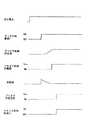
次に、高周波プラズマ処理方法の発明の実施形態の説明も兼ねて、コントローラ7に備えられたシーケンス制御プログラム70について、図2及び図3を使用して説明する。図2は、コントローラ7に備えられたシーケンス制御プログラム70を概略的に示したフローチャート、図3は、図2のシーケンス制御プログラム70おけるプラズマ用電源4とイオン入射用電源50の動作のタイミングについて示すタイミングチャートである。図2に示すフローチャートは、プラズマ形成及びイオン入射用電界の設定の部分を抜粋して概略的に示したものとなっている。尚、図3中、「プラズマ形成の状況」の欄は、放電空間のガスの電離度の推移を概略的に示したものである。電離度が高くなって安定した値に落ち着くと、プラズマが安定的に形成されたとすることができる。
【0021】
処理チャンバー1内は、排気系11により予め所定の真空圧力に排気されている。プラズマ形成は、まず、プロセスガス導入系2によるプロセスガスの導入によりスタートする。コントローラ7は、プロセスガス導入系2に制御信号を送り、プロセスガスを所定の流量で導入させる。また、コントローラ7は、排気系11に制御信号を送り、処理チャンバー1内の圧力を所定の値に維持させる。
プロセスガス導入系2に設けられた不図示の流量計や処理チャンバー1に設けられた不図示の真空計により流量や圧力が所定の値に維持されていることが確認された後、コントローラ7は、まず、プラズマ用電源4を動作させる。この結果、プラズマ用整合器41を介して高周波電極3に高周波電圧が印加され、プラズマが形成される。
この際、コントローラ7は、高周波電極3への高周波電圧の印加開始と同時にタイマーをスタートさせる。そして、タイマーが設定経過時間をカウントすると、コントローラ7は、イオン入射用電源50を動作させる。この結果、基板ホルダーに高周波電圧が印加され、前述したように、基板9に自己バイアス電圧が与えられる。これにより、イオン入射用電界が設定される。
【0022】
上述したシーケンス制御プログラム70において、設定経過時間は、高周波電極3への高周波電圧の印加後、イオン入射用電源50を動作させるまでのタイムラグとして設定された時間である。この設定経過時間は、高周波電極3への高周波電圧印加後、プラズマが安定してから基板ホルダー5にイオン入射用の高周波電圧を印加すべく設定されたものである。以下、この点について説明する。
発明者の研究によると、プラズマ用電源4のようなVHF帯の高周波電源と、イオン入射用電源50のようにHF帯の高周波電源とを同時に動作させて放電を開始させた場合、プラズマが安定状態に移行できず、電源の保護回路等が働いてプラズマ形成が不能になってしまうような事態が生ずることが確認された。以下、この点について説明する。
【0023】
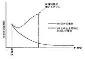
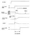
図4は、整合器によってインピーダンス整合を行いながら高周波気体放電によるプラズマ形成を行う場合の反射波の大きさの推移について示した図である。
周知のように、高周波気体放電によるプラズマ形成のメカニズムにおいては、まず、原初的に存在する電子が電界によって加速されて中性ガス分子に衝突して電離させる。電離より生じた二次イオンがさらに別の中性ガス分子に衝突して電離させ、このような過程が繰り返されて、急激に電子とイオンの量が増えて放電が始動する。そして、イオン化したガスの量が多くなり、プラズマ状態に移行する。
【0024】
本実施形態におけるプラズマ用整合器41のように、プラズマ形成用の高周波電源と負荷である放電空間との間に設けられた整合器は、通常、プラズマ形成時に負荷側のインピーダンスが最適なインピーダンスになるよう構成される。つまり、プラズマ形成時に、負荷側のインピーダンスが線路の特性インピーダンスに精度良く一致し、反射波が少なくて最も多くの電力がプラズマに結合するよう構成される。
この際、図4に示すように、高周波電圧の印加後の初期状態においては、放電空間のガスの電離度は低く、空間インピーダンスが高い。従って、整合器によっても最適整合状態から少し外れており、反射波はある程度多い。しかしながら、高周波電力は放電空間に供給されており、供給された電力により中性ガス分子のイオン化が進むと、徐々にガスの電離度は高くなり、ガスはプラズマ状態に近づく。この結果、整合器による最適整合状態に近づくため、反射波も徐々に低減する。そして、プラズマが安定すると、反射波も低い安定した大きさに落ち着く。
【0025】
尚、高周波電源は、通常、出力電圧を一定に維持するよう制御されている。そして、負荷からの反射波をモニタする反射波モニタを有しており、反射波が限度以上に多くなると、自動的に出力電圧をダウンさせて電源を保護する保護回路が設けられている。
このような高周波気体放電によるプラズマ形成において、VHF帯の高周波によってプラズマを形成するものの、何らかの目的でHF帯の高周波も同時に印加すると、図4に示すように、VHF帯の高周波の反射波は低減せず、逆に反射波が大きくなってしまうことがある。
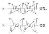
【0026】
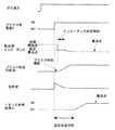
VHF帯の高周波とHF帯の高周波とを電空間に供給すると、放電空間の電界は、VHF帯の高周波がHF帯の高周波により変調された状態となる。この場合、電源側に戻るVHF帯の反射波も、HF帯の高周波で変調された状態となる。図5は、電源側に戻るVHF帯の反射波の状況について示した図である。図5中の(1)は、VHF帯の高周波が最適整合状態で供給されている際にHF帯の高周波が供給された場合の反射波の状況、図5中の(2)は、VHF帯の高周波の供給がまだ最適整合状態でない段階でHF帯の高周波が供給される場合の反射波の状況について示している。
【0027】
図5(1)に示すように、VHF帯が充分に整合が取れた状態で放電空間に供給されている際にHF帯の高周波が供給される場合、元々の反射波が少ないので、HF帯の高周波により変調されてもピーク値として大きな値を持つことはない。しかしながら、図5(2)に示すように、VHF帯の供給が最適整合整合でないときにHF帯の高周波が供給される場合、反射波が大きいので、それがHF帯の高周波により変調された場合、ピーク値として大きな値を持つ。反射波モニタは、この大きなピーク値を捉えて反射波が増大したと判断し、この結果、図4に示すように、保護回路がVHF帯の電源をダウンさせてしまうことがある。
【0028】
本実施形態における設定経過時間は、このような知見及び検討に基づくものである。即ち、高周波電極3からの反射波が限度以上に大きくならないようにしてイオン入射用の高周波を重畳させるため、プラズマ用電源4による高周波電力供給が最適整合状態になった後、イオン入射用電源50を動作させるという技術的意義を有するものである。高周波電極3へのVHF帯の高周波電圧印加後、プラズマが安定して最適整合状態になるまでの時間は、本実施形態では約1秒程度である。従って、安全を見込んで、設定経過時間は2秒に設定されている。
【0029】
次に、高周波プラズマ処理方法の発明の実施形態の説明も兼ねて、本実施形態の装置の全体の動作について概略的に説明する。
基板9は、大気側から不図示のロードロックチャンバーに搬入される。ロードロックチャンバー及び処理チャンバー1が所定の真空圧力まで排気された後、不図示のゲートバルブが開けられ、不図示の搬送系により基板9は処理チャンバー1内に搬入され、基板ホルダー5の上の所定位置に載置される。不図示の吸着電源が動作して、基板9が基板ホルダー5に静電吸着される。
この後、プロセスガス導入系2が動作して所定のエッチング作用のあるガスが所定の流量で導入される。この状態で、前述したようにまずプラズマ用電源4が動作し、高周波放電が生じてプラズマが形成される。そして、設定経過時間の経過後、イオン入射用電源50が動作し、基板9に自己バイアス電圧が与えられる。プラズマ中では、活性種やイオン、もしくはラジカルが生成され、これらの化学種が基板9に達して基板9の表面がエッチングされる。基板9に与えられた自己バイアス電圧により、プラズマ中のイオンは効率良く引き出されて基板9に入射し、エッチングを促進する。
【0030】
例えば、酸化シリコンをエッチングする場合、プロセスガスとして四フッ化炭素と水素の混合ガスが導入される。プラズマ中では、フッ素活性種、フッ素イオン、水素活性種、水素イオンが生成され、これらの化学種は、基板9の表面に存在する酸化シリコンと反応して、フッ化シリコンや水等の揮発物を作り出す。この結果、酸化シリコンがエッチングされる。この際、イオン衝撃エネルギー制御用電圧が基板9に与えられているので、フッ素イオンや水素イオンのエネルギーによりエッチングが促進され、またそれらイオンが基板9により垂直に入射するので、サイドエッチングの少ない良好なエッチング形状が得られる。
【0031】
このようなエッチングを所定時間行った後、プラズマ用電源4、イオン入射用電源50及びプロセスガス導入系2の動作を止める。処理チャンバー1内を再度排気するとともに、基板9の静電吸着を解除する。そして、基板9を基板ホルダー5から取り去り、不図示のロードロックチャンバーを経由して大気側に取り出す。このような動作を繰り返して、各基板9に対してエッチングの枚葉処理を行う。
【0032】
上記構成及び動作に係る本実施形態の装置によれば、プラズマ用電源4によるVHF帯の高周波電力の供給が最適整合状態になってからイオン入射用電源50によるHF帯の高周波電力の供給が開始されるので、反射波が多くなってプラズマ用電源4が出力をダウンさせてしまうような事態が発生しない。従って、プラズマ形成を常に安定して行うことができ、信頼性の高い装置となる。
【0033】
次に、本願発明の第二の実施形態の装置について説明する。
図6は、第二の実施形態に係る高周波プラズマ処理装置の正面断面概略図である。第二の実施形態の装置は、第一の実施形態の装置の構成をさらに最適化するため、プラズマが形成されたことを確認するプラズマ形成確認手段を備えている。また、これに伴い、コントローラ7のシーケンス制御プログラム70も多少変更が加えられている。
【0034】
プラズマ形成確認手段として、処理チャンバー1内に形成されるプラズマをモニタするプラズマモニタ81と、高周波電極3に自己バイアス電圧が与えられたどうかを検出する自己バイアス電圧検出器82とが設けられている。プラズマ形成確認手段の構成としては、これらのいずれか一方のみが設けられている構成でも良い。
プラズマモニタ81は、処理チャンバー1内からの発光を検出することによりプラズマが形成されたかどうかをモニタするものである。具体的には、プラズマモニタ81には、照度計やスペクトルモニタ(分光器)等の光測定器が使用される。尚、処理チャンバー1の側壁には光学窓811が設けられている。光学窓811は、モニタする発光波長の光を充分透過できる材質で設けられており、プラズマモニタ81は光学窓811を通して内部の発光をモニタするようになっている。
【0035】
自己バイアス電圧検出器82は、高周波電極3の電位変化から自己バイアス電圧の大きさを検出するものとなっている。図7は、自己バイアス電圧を説明する図である。図7に示すように、高周波電極3に対しキャパシタンスを介して高周波電圧V1を印加してプラズマを形成した場合、高周波電極3の表面の電位変化は、V2として示すように高周波に負の直流電圧Vdcを重畳したようなものとなる。このVdcが自己バイアス電圧である。
自己バイアス電圧検出器82は、高周波電極3の電位変化をモニタし、その時間平均値又は上下のピーク値の平均値を算出する。そして、その値をアース電位と比較して自己バイアス電圧の大きさを検出するようになっている。尚、図6に示すように、自己バイアス電圧検出器82は、直接的には内導体421の電位をモニタしているが、この部分の電位と高周波電極3の電位とは実効的に同じであるとして良い。
【0036】
図8及び図9を使用して、第二の実施形態におけるシーケンス制御プログラム70について説明する。図8は、第二の実施形態におけるシーケンス制御プログラム70を概略的に示したフローチャート、図9は、図8のシーケンス制御プログラム70おけるプラズマ用電源4とイオン入射用電源50の動作のタイミングについて示すタイミングチャートである。
コントローラ7は、同様に、処理チャンバー1内に所定の流量でプロセスガスが導入され、処理チャンバー1内が所定の真空圧力に維持されていることを確認した後、プラズマ用電源4を動作させる。コントローラ7は、高周波電極3への高周波電圧の印加開始と同時又はその以前から、プラズマモニタ81及び自己バイアス電圧検出器82からの信号の入力させている。
【0037】
高周波電極3への高周波電圧の印加により、前述したように、放電空間に絶縁破壊が生じて放電が開始され、ガスの電離度が急激に高くなり、プラズマの形成が始まる。プラズマ密度(プラズマ中の電子又はイオンの数密度)がある程度高くなると、プラズマモニタ81又は自己バイアス電圧検出器82からの信号により、コントローラ7は、プラズマが形成されたことを確認する。図8に示すように、コントローラ7は、このプラズマ形成確認のタイミングでタイマーのカウントを開始する。
タイマーが設定経過時間をカウントすると、コントローラ7は、イオン入射用電源50を動作させる。この結果、基板ホルダー5に高周波電圧が印加され、前述したように、基板9に自己バイアス電圧が与えられる。これにより、イオン入射用電界が設定される。
【0038】
この第二の実施形態においても、プラズマが安定するのに充分な時間が経過した後にHF帯の高周波電力が供給されるので、反射波の増大によってプラズマ用電源4がダウンしてしまうような事故が生じない。これに加えて、プラズマ用電源4を動作させた後、プラズマの形成を確認してからタイマーのカウントをスタートさせるので、プラズマが形成されていない状態で誤ってイオン入射用電源50を動作させてしまう事故が発生しない。
【0039】
尚、第二の実施形態における設定経過時間については、0秒以上の任意の値を設定することができる。つまり、プラズマ形成確認と同時にイオン入射用電源50を動作させても良い。プラズマが形成される過程で、プラズマモニタ81からの信号及び自己バイアス電圧検出器82からの信号は連続的に大きくなるが、それらがどの程度の大きさになった時点でプラズマが形成されたと確認するかによっても、設定経過時間は適宜変更される。また、プラズマ形成からプラズマが安定化するまでの時間も、圧力等によって変わるので、それらに応じて設定経過時間は適宜変更される。
【0040】
次に、本願発明の第三の実施形態について説明する。
図10は、第三の実施形態に係る高周波プラズマ処理装置の正面断面概略図である。第三の実施形態の装置の大きな特徴点は、プラズマ形成の前後における放電空間のインピーダンスの違いを考慮して装置を最適化したものとなっている。具体的には、第三の実施形態の装置は、図10に示すように、第二の実施形態の装置の構成に加え、プラズマ用整合器41を制御する整合器制御系44を備えている。また、同様の目的でコントローラ7におけるシーケンス制御プログラム70も変更が加えられている。
【0041】
まず、整合器制御系44について説明する。
図11は、第三の実施形態の装置に設けられたプラズマ用整合器41及び整合器制御系44の詳細を示す図である。図11に示すように、プラズマ用整合器41は、抵抗411と、抵抗411の両端とアースとの間に設けられた一対の可変容量コンデンサ412,413とから成っている。抵抗411の一方の側がプラズマ用電源4側、他端が負荷側(高周波電極3側)である。
整合器制御系44は、各可変容量コンデンサ412,413の一方の電極を他方の電極に対して変位させてキャパシタンスを変えるモータ441,442と、モータ441,442のドライバ回路443,444、ドライバ回路443,444に制御信号を送る制御部445等から構成されている。モータ441,442には、高精度のサーボモータが使用される。
【0042】
次に、整合器制御系44が行うプラズマ用整合器41の制御について説明する。図12は、整合器制御系44が行うプラズマ用整合器41の制御について説明した図である。周知のように、インピーダンスマッチングは、負荷側のインピーダンスを線路の特性インピーダンスに一致させて反射波を無くすようにすることである。図12に示すように、本実施形態では、抵抗の両端に並列に設けられた可変容量コンデンサ412,413を制御することでプラズマ用整合器41から負荷側のインピーダンスを調整して整合を取っている。これは、本実施形態のように高周波を使用する装置では、抵抗の変動に比べてキャパシタンスの変動が全体のインピーダンスの変化に与える影響が大きく、キャパシタンスを調整する方が効率的だからである。
上記プラズマ用整合器41の構成において、それが持つインピーダンスは、二つの可変容量コンデンサ412,413が持つキャパシタンスの関数であり、二つのキャパシタンスをC1,C2とすると、インピーダンスZは、Z=f(C1,C2)となる。
【0043】
本実施形態のように高周波による気体放電によりプラズマ形成を行う場合に特に注意しなければならないのは、放電の開始前と放電の開始後では、負荷である放電空間のインピーダンスが大きく変わってしまうことである。放電の開始前には、放電空間にはガスが導入されているものの絶縁体でありインピーダンスは高い。しかしながら、放電が開始されてプラズマが形成されると、プラズマは周知のようにマクロ的には導体に相当するので、インピーダンスが低くなる。プラズマが形成された場合、インピーダンスは、高周波電極3とプラズマとの間のシース容量に大きく依存する。従って、インピーダンス整合も、放電開始前と放電開始後に分けて考える必要がある。
【0044】
ここで、放電開始させるために必要なインピーダンス整合の条件について考えている。放電開始に必要なインピーダンス整合条件とは、放電空間を絶縁破壊させるのに必要な条件である。この条件を達成するC1,C2の範囲(以下、放電開始可能範囲)は、図12に示すように比較的広い。放電開始可能範囲は、放電空間の圧力が高くなると、さらに広がる傾向がある。
一方、放電開始後のインピーダンス整合は、プラズマを効率良く維持できるようにするためのものである。つまり、高周波電極3を介してプラズマに印加される高周波電力のうち、反射波が最も少なく、プラズマに結合する(正確には、プラズマが形成されている放電空間に結合する)高周波電力の割合が最も多くなるようにするのが理想的である。このような理想的な状態が達成されるインピーダンス整合条件は、非常に狭いものであり、いわばピンポイントの条件である。以下、この条件を最良点と呼ぶ。
【0045】
最良点のインピーダンス整合条件は、放電開始可能範囲内に入っている場合もあるが、その外側にある場合が多い。従って、放電開始可能範囲内の条件でインピーダンス整合を行って放電を開始させた後、インピーダンス整合条件を変えて最良点でインピーダンス整合がされるようにすることが最も好ましい。本実施形態の整合器制御系44は、このような考え方のもと、まず、放電開始可能範囲内のインピーダンス整合条件として設定放電開始点でまずインピーダンス整合を行い、その後、最良点でのインピーダンス整合に切り替えている。
【0046】
本実施形態では、設定放電開始点は、予め実験的に求めて定められる。より具体的に説明すると、プロセスガスを導入していない状態で処理チャンバー1内を4Pa程度の真空に保ち、実際の基板9の処理の場合と同程度の電力を高周波電極3に印加する。この場合、放電は生じないが、可変容量コンデンサ412,413を駆動してインピーダンスを変えると、高周波電極3から戻ってくる反射波の大きさを変化する。そして、電圧供給状況モニタ43により、反射波が最も小さくなった際のC1,C2を記憶し、それを設定放電開始点とする。コントローラ7の記憶部72は、このような設定放電開始点を記憶するようになっている。
【0047】
また、最良点でのインピーダンス整合は、本実施形態では、電力供給モニタからの信号に従って自動的に行うようになっている。即ち、制御部445は、電力供給モニタからの信号を常時入力させており、進行波に対する反射波の大きさが常時モニタされている。そして、進行波に対する反射波の大きさが最も小さくなるよう、整合器制御系44に制御信号を送る。
より具体的に説明すると、二つの可変容量コンデンサ412,413のうちの一方を第一コンデンサ412としこれを駆動するモータ441を第一モータ441とする。また、他方の可変容量コンデンサ413を第二コンデンサ413としこれを駆動するモータ442を第二モータ442とする。第一第二コンデンサ412,413において、キャパシタンスを多くする向きを+方向、少なくする向きを−方向とする。
【0048】
制御部445は、第一コンデンサ412が例えば+方向に駆動されるようドライバ回路443に信号を送る。この際、反射波が増加したら逆に−方向に第一コンデンサ412が駆動されるようにする。+方向又は−方向に駆動させた際、反射波が減少していき、極小値を越えて上昇に転じたら、−方向又は+方向に逆転させる。第一モータ441はサーボモータであり、反射波が極小値を取るよう、常に第一コンデンサ412を駆動する。第二コンデンサ413を駆動する第二モータ442についても同様であり、反射波が極小値となるようサーボ制御が行われる。
【0049】
図12には、上述した整合器制御系44における制御の結果、C1,C2がどのように変化していくかが軌跡として示されている。図12に示すように、C1,C2は、最初は設定放電開始点に一致し、この状態で放電が開始される。放電が開始した後、電力供給状況モニタ43による自動制御になり、C1,C2は不安定に変化する。そして、プラズマが安定化すると、C1,C2も最良点に一致した状態で安定化する。プラズマが安定化すると、二つの可変容量コンデンサ412,413の駆動量(モータ441,442の回転量)は極小値になる。整合器制御系44は、二つの可変容量コンデンサ412,413の駆動量をコントローラ7に常時出力している。コントローラ7は、二つの可変容量コンデンサ412,413の駆動量がある設定値以下の大きさになったことを確認すると、プラズマが安定したと判断する。
尚、最良点のインピーダンス整合条件は、常に一定という訳ではなく、各回のプラズマ処理において異なる場合がある。これは、処理条件(処理チャンバー1内の圧力やプロセスガスの種類等)が変わった場合に生ずるが、それだけではなく、処理チャンバー1の内壁面に堆積物が生じたりする場合にも生ずる。整合器制御系44は、そのときどきの最良点になるようプラズマ用整合器41を制御する。
【0050】
次に、本実施形態におけるシーケンス制御プログラム70について、図13及び図14を使用して説明する。図13は、第三の実施形態におけるシーケンス制御プログラム70を概略的に示したフローチャート、図14は、図13のシーケンス制御プログラム70おけるプラズマ用電源4とイオン入射用電源50の動作のタイミングについて示すタイミングチャートである。尚、図14中の「整合用インピーダンス」の欄は、プラズマ用整合器41のインピーダンスの大きさの推移を例示的に且つ模式的に示したものである。
【0051】
コントローラ7は、同様に、処理チャンバー1内に所定の流量でプロセスガスが導入され、処理チャンバー1内が所定の真空圧力に維持されていることを確認した後、プラズマ用電源4を動作させる。この際、コントローラ7は、前述した放電開始点の条件でインピーダンス整合が予め行われるよう、整合器制御系44の制御部445に信号を予め送っている。整合器制御系44は、放電開始点の条件になるよう、二つの可変容量コンデンサ412,413を予め駆動しておく。プラズマ用電源4によって高周波電極3に高周波電圧が印加されると、前述したように、放電空間に絶縁破壊が生じて放電が開始され、プラズマが形成される。コントローラ7は、高周波電極3への高周波電圧の印加開始と同時又はその以前から、プラズマモニタ81及び自己バイアス電圧検出器82からの信号を入力させている。
【0052】
コントローラ7は、プラズマモニタ81もしくは自己バイアス電圧検出器82又はその双方からの信号により、放電が始動してプラズマが形成されたことを確認すると、整合器制御系44に制御信号を送り、インピーダンス整合条件を変える。即ち、前述した最良点で整合が取れるようにする自動制御に切り替えるよう整合器制御系44に信号を送る。と同時に、コントローラ7は、タイマーのカウントをスタートさせる。
整合器制御系44は、前述したように電力供給状況モニタ43からの信号により二つの可変容量コンデンサ412,413を駆動し、最良点になるよう自動制御を行う。コントローラ7は、タイマーのカウントが設定経過時間に一致したら、前述した実施形態と同様に、イオン入射用電源50を動作させる。この結果、基板ホルダー5に高周波電圧が印加され、前述したように、基板9に自己バイアス電圧が与えられる。これにより、イオン入射用電界が設定される。
【0053】
本実施形態の装置においても、プラズマが安定するのに充分な時間が経過した後にHF帯の高周波電力が供給されるので、反射波の増大によってプラズマ用電源4がダウンしてしまうような事故が生じない。プラズマが安定するのに充分な時間が経過した後にHF帯の高周波電力が供給されるので、反射波の増大によってプラズマ用電源4がダウンしてしまうような事故が生じない。
これに加え、放電開始点のインピーダンス整合条件下で放電が開始され、プラズマの形成を確認した後、最良点でインピーダンス整合が取れた状態になるようにする自動制御が行われるので、放電開始時及びプラズマ形成後ともに最適なインピーダンス整合の状態が確保される。このため、放電開始時及びプラズマ形成後ともに、反射波が少なく、放電の開始やプラズマの維持にための電力効率が高くなる。
【0054】
尚、第三の実施形態において、プラズマ安定維持のため、前述した最良点になるようにする自動制御を行うことは必ずしも必須条件ではない。例えば、プラズマ安定維持に最適なプラズマ用整合器41におけるインピーダンス値(設定最良点)を予め求めておき、プラズマ形成確認後、放電開始点からその設定最良点にスイッチするだけで良い場合もある。また、プラズマ形成確認後、設定最良点にスイッチし、その状態からさらに最良点になるようにする自動制御を行っても良い。
【0055】
尚、放電開始に適した条件でのインピーダンス整合からプラズマ安定維持に適した条件でのインピーダンス整合への切り替えは、プラズマ形成確認手段によるプラズマ形成確認と同時であったが、それからさらに少しタイムラグをおいた方が良い場合もある。例えば、3Pa程度以下の低圧で放電を開始させる場合、放電開始後プラズマが安定状態に移行するまでに多少長い時間を要する。この時間は長くても3秒を越えることはない。従って、プラズマ用電源4への高周波電圧印加後、安全を見込んで6秒程度経過した際にプラズマ安定維持に適したインピーダンス整合条件に切り替えるようにすると好適である。この場合も、プラらズマ安定維持に適したインピーダンス整合条件に切り替えてから2秒程度経過した後、イオン入射用電源50を動作させる。
【0056】
また、この第三の実施形態において、イオン入射用電源50については、基板の処理の際に供給されるべき値として設定された設定値にその供給電力が達するまで0.5秒以上6秒以下となるよう、徐々にその供給電力を増加させることが好ましい。いきなり設定値の電力を印加すると、放電空間の条件やプラズマの状態が大きく変化してしまう。この場合、そのような変化が大きいと、プラズマ用電源4の自動制御が追従できなくなり、インターロックが働いてプラズマ用電源4がダウン(自己保護のための出力停止)してしまう可能性がある。このような事故が無いようにするには、イオン入射用電源50は、動作開始後、0.5秒以上かけて設定値にもっていくようにすることが好ましい。尚、この時間が6秒を越えると、生産性の点で問題が生ずるので、6秒以下とすることが好ましい。
【0057】
次に、本願発明の第四の実施形態について説明する。第四の実施形態の装置は、シーケンス制御プログラム70の構成が第三の実施形態と異なっている。他の部分は基本的に同一である。図15は、第四の実施形態におけるシーケンス制御プログラム70を概略的に示したフローチャート、図16は、図15のシーケンス制御プログラム70おけるプラズマ用電源4とイオン入射用電源50の動作のタイミングについて示すタイミングチャートである。
【0058】
第四の実施形態の装置の大きな特徴点は、電力供給状況モニタ43からの信号により、プラズマが安定したことを確認した後、イオン入射用電源50を動作させることである。具体的に説明すると、第三の実施形態と同様に、放電開始点の条件でプラズマ用電源4を動作させてプラズマを形成する。電力供給状況モニタ43は、進行波に対する反射波の相対的な割合を計測し、そのデータをADコンバータ75を介してコントローラ7に送る。コントローラ7は、プラズマ形成確認手段からの信号によりプラズマ形成を確認した後、最良点での自動制御に切り替える。自動制御の過程で、プラズマは安定状態に移行する。
【0059】
プラズマが安定状態に移行する過程で、図16に示すように、反射波が徐々に低下していく。コントローラ7は、反射波が所定の基準値以下の低い値に安定したかどうかを判断し、これが真値であった場合、これをもってプラズマが安定したとする。コントローラ7は、このタイミングでイオン入射用電源50を動作させ、イオン入射用電界を設定する。
【0060】
本実施形態の装置によれば、上述した効果に加え、プラズマの安定化を確認してからイオン入射用電源50を動作させるので、プラズマ形成後、何らかの事情で安定状態に移行していないにもかかわらず、イオン入射用電源50が動作してしまう事故が発生しない。反射波がどの程度まで低下したらプラズマが安定化したと判断するかについては、例えば、「進行波の20%以下に低下した場合」とすることができる。
【0061】
次に、本願の第五の実施形態について説明する。第五の実施形態の装置も、シーケンス制御プログラム70の構成が他の実施形態と異なっている。それ以外の部分は基本的に同一である。図17は、第五の実施形態におけるシーケンス制御プログラム70を概略的に示したフローチャート、図18は、図17のシーケンス制御プログラム70おけるプラズマ用電源4とイオン入射用電源50の動作のタイミングについて示すタイミングチャートである。
第五の実施形態の装置におけるコントローラ7は、同様に、放電開始点の条件でプラズマ用電源4を動作させて放電を開始する。この際、プラズマ用電源4の動作開始から、コントローラ7は、整合器制御系44の制御を、最良点になるようにする自動制御とする。また、第一の実施形態と同様に、プラズマ用電源4と同時にタイマーのカウントをスタートさせる。
【0062】
放電が開始されてガスの電離度が高まるにつれ、反射波も徐々に低下する。これに追従するようにして整合器制御系44がインピーダンスを変えるので、整合用インピーダンスは図18に示すように不安定に変化する。そして、プラズマが安定化すると、反射波の低下も落ち着いて安定化するので、整合用インピーダンスもある値に落ち着く。
プラズマが安定化するのに要する時間よりも充分に長い時間に設定されている設定経過時間をタイマーがカウントすると、コントローラ7は、コントローラ7は、イオン入射用電源50を動作させる。この結果、イオン入射用電界が設定される。
この実施形態の構成によれば、プラズマ形成確認手段が不要になり、この点で装置が簡略化できるメリットがある。
【0063】
尚、この第五の実施形態においても、タイマーによる設定経過時間のカウントによらず、電力供給状況モニタ43からの信号によりプラズマの安定化を確認した際にイオン入射用電源50を動作させても良い。
また、プラズマの安定化確認は、電力供給状況モニタ43からの信号によらず、整合器制御系44からの信号によっても良い。即ち、上述したように、プラズマが安定化すると、可変容量コンデンサ412,413の駆動量が殆どゼロになり、整合用インピーダンスはある値に落ち着く。従って、前述したように、可変容量コンデンサ412,413の駆動量をモニタしてそのデータをコントローラ7に送るようにし、このデータからプラズマ安定化を確認しても良い。
【0064】
次に、本願の第六の実施形態について説明する。第六の実施形態の装置も、シーケンス制御プログラム70の構成が他の実施形態と異なっている。それ以外の部分は基本的に同一である。図19は、第六の実施形態におけるシーケンス制御プログラム70を概略的に示したフローチャート、図20は、図19のシーケンス制御プログラム70おけるプラズマ用電源4とイオン入射用電源50の動作のタイミングについて示すタイミングチャートである。
【0065】
第六の実施形態の装置におけるコントローラ7は、同様に、放電開始点の条件でプラズマ用電源4を動作させて放電を開始する。電力供給状況モニタ43は、進行波に対する反射波の相対的な割合を計測し、そのデータをADコンバータ75を介してコントローラ7に送る。コントローラ7は、プラズマ形成確認手段からの信号によりプラズマ形成を確認した際、まず、インピーダンス整合条件を設定最良点とするとともに、タイマーのカウントをスタートさせる。コントローラ7は、インピーダンス整合条件を設定最良点に固定して維持し、タイマーのカウントが所定の経過時間(以下、インピーダンス固定時間)に達したら、自動制御に切り替える。そして、前述した第3の実施形態と同様、自動制御が安定するまの時間が経過した後、イオン入射用電源50を動作させる。
【0066】
この実施形態の構成は、放電開始点でのインピーダンス整合から自動制御によるインピーダンス整合への切り替えをより確実にスムーズにする技術的意義がある。以下、この点について説明する。
前述した第三の実施形態において、放電開始点でのインピーダンス整合から自動制御に切り替えた際、前述したように、最良点になるよう整合器制御系が動作する。整合器制御系は、整合用インピーダンスを調節し、より反射波が少なくなるようにする。これにより、プラズマに投入されるパワーが増し、電離度が高くなる。そして、これに伴い、プラズマのインピーダンスも変化するので、それに追従するように整合器制御系が自動制御を行う。そして、プロセスガスが殆どすべて電離し、プラズマの状態が安定すると、最良点となり、プラズマへの投入パワーも安定して整合用インピーダンスもある一定に落ち着く。
【0067】
しかしながら、自動制御を開始した直後の段階で、反射波がある程度大きい場合、目的とする状態からかなり外れた状態で整合を取るよう自動制御が行われてしまうことがある。具体的に説明すると、放電開始点と最良点との差異が比較的大きい場合、放電開始点でのインピーダンス整合から自動制御に切り替えた直後では、ある程度大きな反射波が存在している場合がある。その場合にも、自動制御により、前述したように最良点に落ち着く筈なのであるが、反射波がある一定以上存在している場合、最良点に落ち着く前にプラズマ用電源4の保護回路が働き、プラズマ用電源4は出力を大きくダウンさせてしまうことがある。
【0068】
こうなると、プラズマへの投入パワーが大きく変化する結果、プラズマの状態(プラズマシースの厚さ、シース電位、プラズマ密度等)も大きく変化してしまう。そして、この変化したプラズマの状態において最良点になるよう自動制御が続行されるので、結果的に、目的としていた状態からかなり外れた状態で整合を取ろうとすることになってしまう。つまり、かなり投入パワーの低い状態で整合を取ろうとすることになってしまう。従って、整合が取れたとしても、プラズマ密度がかなり低い等、正しい処理条件とは異なる処理条件となってしまう。
【0069】
一方、この第六の実施形態によれば、放電開始点での制御から自動制御に切り替える前に、設定最良点で固定して一定時間維持する制御を行う。設定最良点は、圧力、プロセスガスの流量、印加電圧等の諸条件に従い、自動制御において到達するであろう最良点を予め予想して、実験的に又は理論的に定めておく。設定最良点の条件を一定時間維持する間に、プロセスガスの電離がほぼ飽和する等、プラズマの状態が最良点に近い状態となる。この状態から自動制御が開始されるので、自動制御開始時における反射波は上記第三の実施形態に比べてかなり小さい。従って、目的する状態から外れた状態でインピーダンス整合が取られることがなく、正しい条件での処理を常に行うことができる。このため、再現性や信頼性の点で優れたプラズマ処理装置となる。尚、このような技術的意義は、放電開始点でのインピーダンス整合を予め行う場合に限られるものではなく、最良点の自動制御を行う場合一般に妥当する。また、設定最良点に固定して維持する時間は、好ましくは0.5秒以上5秒以下、例えば1秒程度でよい。
【0070】
次に、本願の第七の実施形態について説明する。第七の実施形態の装置も、シーケンス制御プログラム70の構成が他の実施形態と異なっている。それ以外の部分は基本的に同一である。図21は、第七の実施形態に係る高周波プラズマ処理装置の正面断面概略図、図22は、第七の実施形態におけるシーケンス制御プログラム70を概略的に示したフローチャート、図23は、図22のシーケンス制御プログラム70おけるプラズマ用電源4とイオン入射用電源50の動作のタイミングについて示すタイミングチャートである。
【0071】
第七の実施形態では、次の二つのポイントが前述した各実施形態と異なっている。一つめは、放電開始点の条件でプラズマ用電源4をスタートさせた後、所定時間内にプラズマの形成が確認されなかった場合、リセットをしてプログラムを最初からやり直す点である。二つめは、プラズマ用電源4に加えてイオン入射用電源50の投入電力制御も最適化している点である。
具体的に説明すると、図21に示すように、本実施形態では、イオン入射用整合器51を制御する整合器制御系53を備えている。コントローラ7は、この整合器制御系53も制御可能となっている。また、整合器制御系53は、イオン入射用電源50が高周波を供給する際の進行波に対する反射波の大きさを常時モニタする不図示の電力供給モニタを含んでおり、進行波に対する反射波の大きさが最も小さくなるインピーダンス整合条件を自動制御することが可能となっている。
【0072】
図22に示すように、第七の実施形態の装置におけるコントローラ7は、同様に、放電開始点の条件でプラズマ用電源4を動作させて放電を開始させる。同時に、タイマーのカウントをスタートさせる。電力供給状況モニタ43は、進行波に対する反射波の相対的な割合を計測し、そのデータをADコンバータ75を介してコントローラ7に送る。
図22に示すように、タイマーが所定の経過時間をカウントするまで、プラズマ形成確認手段によるプラズマ形成の確認が成されなかった場合、シーケンス制御プログラム70は、プラズマ用電源4を一旦オフにし、タイマーのカウントをゼロに戻す。そして、スタートに戻り、放電開始点の条件で再びプラズマ用電源4を動作させる。
【0073】
所定の経過時間内にプラズマ形成確認手段からの信号によりプラズマ形成を確認した場合、コントローラ7は、まず、インピーダンス整合条件を設定最良点とするとともに、タイマーをゼロに戻してカウントをスタートさせる。コントローラ7は、インピーダンス整合条件を設定最良点に固定して維持し、タイマーのカウントが所定の経過時間(以下、インピーダンス固定時間)に達したら、自動制御に切り替える。そして、前述した第三の実施形態と同様、自動制御が安定するまの時間が経過した後、イオン入射用電源50を動作させる。
この際、図23に示すように、イオン入射用電源50は、徐々に投入電力を増加させ、イオン入射のために最終的に必要な投入電力に到達させるようになっている。例えば、イオン入射用電源50が1.6MHzのHF電源であり、最終的な投入電力が1.8kWである場合、1秒程度の時間で0kWから1.8kWに到達させる。尚、この際、整合器制御系53は、イオン入射用整合器51のインピーダンスを固定された値に保持する。
【0074】
さらに、図22に示すように、シーケンス制御プログラム70は、イオン入射用電源50からの投入電力が切替基準値になった時点で、整合器制御系53に信号を送り、イオン入射用整合器51を自動制御に切り替えさせる。切替基準値は、ある程度小さな値であり、例えば、最終的な投入電力1.8kWである場合、10Wである。イオン入射用整合器51が自動制御に切り替わる結果、イオン入射用電源50から基板ホルダ5に供給される高周波の反射波が最も小さくなる。そして、この状態を保ちながら、イオン入射用電源50の投入電力は徐々に増加し、最終的に必要な電力に達したら、その値を保持するよう制御される。
【0075】
本実施形態の構成は、以下のような技術的意義を有する。
まず、プラズマ用電源4の動作開始後、所定の経過時間内にプラズマ形成が確認されなかった場合、プログラムがリセットされてスタートに戻るので、何らかの事情でプラズマの形成が確認されない場合、プラズマ用電源4が動作し続けてしまう問題がない。場合によっては、リセットの回数をカウントしておき、所定回数(例えば3回)リセットしてもプラズマの形成が確認されない場合、プログラムを完全に中止し、エラー信号を発生するようにしてもよい。
【0076】
また、イオン入射用電源50の投入電力を徐々に増加させる点は、プラズマ用電源4の自動制御との関連で顕著な技術的意義を有する。即ち、プラズマ用電源4の自動制御が行われている状態でイオン入射用電源50の投入電力を一気に設定値(イオン入射に必要な電力値)に増加させると、プラズマのインピーダンス条件が急激に変化するため、プラズマ用電源4の自動制御が不安定化する恐れがある。プラズマ用整合器41は、自動制御のため、そのインピーダンスが激しくふらついた後、やがて安定した値に落ち着くが、あまりにもプラズマのインピーダンス条件の変化が激しいと、整合器制御系44の追従制御可能な範囲を越えてしまい、いつまで経ってもプラズマ用整合器41のインピーダンスが安定化しなくなってしまうこともあり得る。
本実施形態の構成によれば、イオン入射用電源50の投入電力が徐々に増加するので、このような問題はなく、プラズマ用整合器41のインピーダンスも、短時間のうちに安定化する。従って、イオン入射用電源50の投入電力を徐々に増加させるとは、整合器制御系44が追従してプラズマ用整合器41の自動制御を行える範囲内にプラズマのインピーダンス条件変化を抑えるよう徐々に増加させる、という意味である。
【0077】
尚、上述した第三乃至第七の実施形態において、最良点になるようにする自動制御が開始される際、初期の整合用インピーダンスは放電開始点の条件になるようにするものであったが、前回の基板処理の終了時の整合用インピーダンスを記憶して保持し、これを初期設定として用いても良い。この場合、処理チャンバー1内の環境等に大きな変化が無い限り、整合用インピーダンスも大きく変化することがない。この構成は、放電開始時の最適整合条件と、プラズマ維持の際の最適整合条件とがそれほど変わらない場合に好適である。
尚、各実施形態において、設定経過時間は、プラズマの安定化に要する時間であり、2秒とされたが、もっと長い時間とされる場合もある。プラズマの安定化に要する時間は、装置の構造や放電空間の大きさ、圧力などによって変化する。従って、これらの要素を考慮に入れて設定経過時間は適宜変更される。
【0078】
また、プラズマの安定維持のためのインピーダンス整合は、前述したような自動制御によらなくても本願発明は実施可能である。例えば、プラズマ安定維持に適したインピーダンス整合条件を予め実験的に求めて設定し、この設定された条件で固定してインピーダンス整合を行っても良い。また、プラズマの形成を確認した後、放電開始点から、プラズマ安定維持用に設定された条件に変更した後、そこからさらに自動制御に変更しても良い。
尚、各実施形態において、複数のADコンバータ75をまとめて1つにした構成が採用されることもある。即ち、タイムシェアリングによって1つのADコンバータ75によって複数のデータをデジタル化する場合もある。
【0079】
上述した各実施形態では、第一の周波数の高周波はVHF帯、第二の周波数の高周波はHF帯であったが、本願発明はこれに限られる訳ではない。異なる二つの周波数を印加した場合の変調現象は一般的に見られるものであり、本願発明の構成は、これに起因した問題を解決する技術的意義がある。
また、HF帯の高周波は、基板9に自己バイアス電圧を与えてイオン入射用の電界を設定するものであったが、他の目的の場合もあり得る。例えば、自己バイアス電圧を利用して基板9を基板ホルダー5に静電吸着する場合等である。
【0080】
上記各実施形態では、基板処理の一例としてエッチングを採り上げたが、スパッタリングやプラズマ化学蒸着(CVD)等の成膜処理、表面酸化や表面窒化等の表面改質処理、さらにはアッシング処理等を行う装置についても、同様に実施することができる。
処理対象である基板9としては、半導体ウェーハの他、液晶ディスプレイやプラズマディスプレイ等の表示デバイス用の基板、磁気ヘッド等の磁気デバイス用の基板等を対象とすることができる。
【0081】
【発明の効果】
以上説明した通り、本願の請求項1の方法又は請求項14の装置によれば、第一の周波数の高周波によりプラズマが形成されプラズマが安定化した後に第二の周波数の高周波が印加されるので、第二の周波数の高周波の影響による反射波の増大のような問題が第一の周波数の高周波の印加について生じない。また、上記効果に加え、放電空間に結合する高周波電力が最大となるようインピーダンス整合が自動制御により行われるので、電力の効率が常に高く維持される。
また、請求項2の方法又は請求項15の装置によれば、上記効果に加え、VHF帯の高周波によってプラズマを形成しつつHF帯の高周波を特定の目的のために利用することができる。
また、請求項3の方法又は請求項16の装置によれば、基板に自己バイアス電圧を与えながら上記効果を得てプラズマ処理を行うことができる。
また、請求項7の方法又は請求項20の装置によれば、上記効果に加え、放電の開始の際と、プラズマの安定維持の際とで、それぞれ異なる最適なインピーダンス整合条件で整合が行われるので、放電開始時及びプラズマ形成後ともに、反射波が少なく、放電の開始やプラズマの維持にための電力効率が高くなる。
また、請求項8の方法又は請求項21の装置によれば、上記効果に加え、プラズマの安定維持のためのインピーダンス整合条件への変更が、プラズマの形成を確認した際又はその後に行われるので、インピーダンス整合条件の変更が誤って行われる事故が発生しない。
また、請求項9の方法又は請求項22の装置によれば、上記効果に加え、自動制御開始時における反射波を小さくできるので、目的する状態から外れた状態でインピーダンス整合が取られることがなく、正しい条件での処理を常に行うことができる。このため、再現性や信頼性の点で優れた方法又は装置となる。
また、請求項10の方法又は請求項23の装置によれば、上記効果に加え、放電の開始の際と、プラズマの安定維持の際とで、それぞれ異なる最適なインピーダンス整合条件で整合が行われるので、放電開始時及びプラズマ形成後ともに、反射波が少なく、放電の開始やプラズマの維持にための電力効率が高くなる。
また、請求項11の方法又は請求項24の装置によれば、上記効果に加え、第二の周波数の高周波電力の投入においてインピーダンス整合の自動制御が行われるので、第二の周波数の高周波電力の投入効率が高くなる。
また、請求項12の方法又は請求項25の装置によれば、上記効果に加え、自動制御を行う際の初期のインピーダンス整合条件が、前回の基板の処理の終了時の条件と同じとされるので、放電開始時の最適整合条件と、プラズマ維持の際の最適整合条件とがそれほど変わらない場合に好適である。
また、請求項13の方法又は請求項26の装置によれば、自動制御開始時における反射波を小さくできるので、目的する状態から外れた状態でインピーダンス整合が取られることがなく、正しい条件での処理を常に行うことができる。このため、再現性や信頼性の点で優れた方法又は装置となる。
【図面の簡単な説明】
【図1】第一の実施形態に係る高周波プラズマ処理装置の正面断面概略図である。
【図2】図1に示すコントローラ7に備えられたシーケンス制御プログラム70を概略的に示したフローチャートである。
【図3】図2のシーケンス制御プログラム70おけるプラズマ用電源4とイオン入射用電源50の動作のタイミングについて示すタイミングチャートである。
【図4】整合器によってインピーダンス整合を行いながら高周波気体放電によるプラズマ形成を行う場合の反射波の大きさの推移について示した図である。
【図5】電源側に戻るVHF帯の反射波の状況について示した図である。
【図6】第二の実施形態に係る高周波プラズマ処理装置の正面断面概略図である。
【図7】自己バイアス電圧を説明する図である。
【図8】第二の実施形態におけるシーケンス制御プログラム70を概略的に示したフローチャートである。
【図9】図8のシーケンス制御プログラム70おけるプラズマ用電源4とイオン入射用電源50の動作のタイミングについて示すタイミングチャートである。
【図10】第三の実施形態に係る高周波プラズマ処理装置の正面断面概略図である。
【図11】第三の実施形態の装置に設けられたプラズマ用整合器41及び整合器制御系44の詳細を示す図である。
【図12】図10及び図11に示す整合器制御系44が行うプラズマ用整合器41の制御について説明した図である。
【図13】第三の実施形態におけるシーケンス制御プログラム70を概略的に示したフローチャートである。
【図14】図13のシーケンス制御プログラム70おけるプラズマ用電源4とイオン入射用電源50の動作のタイミングについて示すタイミングチャートである。
【図15】第四の実施形態におけるシーケンス制御プログラム70を概略的に示したフローチャートである。
【図16】図15のシーケンス制御プログラム70おけるプラズマ用電源4とイオン入射用電源50の動作のタイミングについて示すタイミングチャートである。
【図17】第五の実施形態におけるシーケンス制御プログラム70を概略的に示したフローチャートである。
【図18】図17のシーケンス制御プログラム70おけるプラズマ用電源4とイオン入射用電源50の動作のタイミングについて示すタイミングチャートである。
【図19】第六の実施形態におけるシーケンス制御プログラム70を概略的に示したフローチャートである。
【図20】図19のシーケンス制御プログラム70おけるプラズマ用電源4とイオン入射用電源50の動作のタイミングについて示すタイミングチャートである。
【図21】第七の実施形態に係る高周波プラズマ処理装置の正面断面概略図である。
【図22】第七の実施形態におけるシーケンス制御プログラム70を概略的に示したフローチャートである。
【図23】図22のシーケンス制御プログラム70おけるプラズマ用電源4とイオン入射用電源50の動作のタイミングについて示すタイミングチャートである。
【符号の説明】
1 処理チャンバー
11 排気系
2 プロセスガス導入系
3 高周波電極
4 プラズマ用電源
41 プラズマ用整合器
411 抵抗
412 可変容量コンデンサ
413 可変容量コンデンサ
43 電力供給状況モニタ
44 整合器制御系
441 モータ
442 モータ
443 ドライバ回路
444 ドライバ回路
445 制御部
5 基板ホルダー
50 イオン入射用電源
51 イオン入射用整合器
53 整合器制御系
7 コントローラ
70 シーケンス制御プログラム
75 ADコンバータ
81 プラズマモニタ
82 自己バイアス電圧検出器
9 基板[0001]
BACKGROUND OF THE INVENTION
The invention of the present application relates to processing using plasma formed by high-frequency energy, and particularly to processing using high frequencies of two different frequencies.
[Prior art]
[0002]
Processing using plasma formed by high-frequency energy (hereinafter simply referred to as high-frequency plasma processing) is actively used in the manufacture of semiconductor devices such as LSI (Large Scale Integrated Circuit) and display devices such as LCD (Liquid Crystal Display). Yes. In such a high-frequency plasma treatment, a higher frequency such as a VHF band is increasingly used. Hereinafter, this point will be described.
One major factor that increases the frequency of high frequencies is the need for a low pressure process. The demand for low process pressure is closely related to the high integration of devices and the miniaturization of circuits. If the circuit is further miniaturized, there is a high possibility that a product failure will occur even if a small amount of foreign matter (dust, particles, etc.) is mixed. Therefore, it is necessary to prevent such foreign matters from being mixed by lowering the pressure in the processing chamber.
[0003]
In addition, the low pressure of the process is an important issue from the viewpoint of enabling finer processing. For example, as the circuit becomes finer, the aspect ratio of holes such as contact holes and via holes tends to increase. As a technique for forming a hole with a high aspect ratio, reactive ion etching (RIE) is often used in which ions in plasma are extracted and incident on a substrate. In order to form holes with a high aspect ratio by ion incidence, it is important that many ions are accelerated and incident in a direction perpendicular to the substrate. However, when the pressure is high, ions collide with gas molecules and change their directions, so that they are likely to enter the substrate obliquely. As a result, there is a problem that a large number of ions are incident on the side wall of the hole to form a so-called middle-bulged (Boeing) hole.
[0004]
Further, in plasma chemical vapor deposition (CVD) in which a thin film is formed by utilizing a gas phase reaction in plasma, a high pressure increases the possibility that active species generated in the plasma are deactivated by collision. As a result, a large amount of unreacted product called dust remains and tends to deteriorate the atmosphere in the processing chamber. In addition, by-products with low vapor pressure may be evaporated and released from the surface of the substrate during film formation, but when the pressure in the processing chamber is high, it returns to the substrate again and remains, The quality of the thin film may be impaired.
[0005]
For these reasons, the demand for a low pressure process has become prominent. On the other hand, there is still a strong demand for a high-speed process for improving productivity along with a low-pressure process. In order to increase the process speed, it is generally necessary to increase the plasma density (number density of charged particles in the plasma). However, speeding up the process and lowering the process are conflicting demands in some respects. In other words, since the number of gas molecules decreases as the pressure is lowered, the plasma density must be lowered.
[0006]
In order to maintain the plasma density sufficiently high even when the pressure is lowered, it is important to increase the plasma formation efficiency. This is the reason why higher frequency high frequencies are being used in high frequency plasma processing. More specifically, in the previous plasma processing, the high frequency of the MF band to the HF band is often used, but recently, the high frequency of the VHF band has been frequently used. As the frequency increases, the period at which the electrons follow the electric field and change the direction of movement is shortened. As a result, the frequency of collision between electrons and neutral gas molecules increases, and plasma formation efficiency is improved.
[0007]
However, when processing is performed using plasma formed by a higher frequency such as the VHF band, another problem may occur from the viewpoint of maintaining high processing quality and reproducibility. For example, as seen in the RIE described above, in plasma processing, ions are often extracted from the plasma and incident on the substrate. For the incidence of ions, it is necessary to set an electric field whose potential gradually decreases toward the substrate between the plasma and the substrate. This electric field generally corresponds to a sheath electric field that appears between the solid and the plasma when the plasma contacts the solid. If the substrate is made to have a floating potential by insulating the substrate from the ground, a negative sheath electric field can be applied to plasma having a plasma potential (≈0 V).
[0008]
With this negative sheath electric field, ions can be extracted from the plasma and made incident on the substrate. However, when the frequency of the high frequency for plasma formation is increased to about the VHF band, the problem of the sheath electric field becoming smaller becomes a problem. is there. This is because the frequency is so high that it is difficult to follow changes in the electric field not only for ions but also for electrons. By applying a high frequency through the substrate, the above-described ion incidence is often performed by applying a self-bias voltage to the substrate. However, when the frequency increases to about the VHF band, the electrons follow the electric field. Thus, there is a problem that a sufficiently large self-bias voltage cannot be applied because the amount of movement decreases.
Moreover, in plasma CVD etc., since the incident amount and incident energy of ions on the substrate affect the processing, it is necessary to maintain them in the optimum range. However, apart from that, there is an optimum application condition of high frequency for forming plasma, and in many cases, both are incompatible.
In consideration of such points, recently, a configuration has been adopted in which a high frequency in the VHF band is applied for plasma formation, and a high frequency in the HF band having a frequency lower than the VHF band is separately applied for ion incidence to the substrate. It is becoming.
[0009]
[Problems to be solved by the invention]
However, according to the research of the inventors of the present application, when plasma is formed by applying high frequencies of two different frequencies, such as the VHF band and the HF band, since the high frequency coupling to the plasma becomes insufficient, the plasma is insufficient. It has been found that there is a problem that the plasma is not maintained well or the plasma becomes unstable in the initial state.
The invention of the present application has been made to solve such a problem. In high-frequency plasma processing in which plasma is formed using two high-frequency frequencies, the formation and maintenance of the plasma is sufficiently and stable. It has the technical significance of making it possible to enjoy the benefits of using these two frequencies.
[0010]
[Means for Solving the Problems]
In order to solve the above-mentioned problems, an invention according to
A first step of supplying high-frequency power of a first frequency to the discharge space to start high-frequency discharge;
After a high frequency discharge is started, a high frequency power having a second frequency different from the first frequency is supplied to the discharge space after a predetermined time lag necessary for the plasma to form and stabilize the plasma has elapsed. The second step andHave
The first step is to start discharge by supplying high-frequency power under a first impedance matching condition suitable for the start of the high-frequency discharge. After that, the impedance matching condition is suitable for plasma stabilization. Including changing to the second impedance matching condition,
The second impedance matching condition is a condition in which the magnitude of the high-frequency power coupled to the discharge space in which the plasma is formed has a maximum value or the reflected wave from the discharge space has a minimum value. The step is a step of automatically controlling the matching impedance so as to be in this state by monitoring the supply state of the high frequency power to the discharge space.It has the composition.
In order to solve the above problems, the claims14The described invention includes a processing chamber in which a substrate to be processed is disposed, a process gas introduction system for introducing a process gas into the processing chamber, a high-frequency electrode provided in the processing chamber, and a high-frequency electrode to the high-frequency electrode. A first high-frequency power source for forming a process gas plasma by setting a high-frequency electric field in the processing chamber by applying a voltage to generate a high-frequency discharge, and performing a predetermined process on the substrate using the plasma A high-frequency plasma processing apparatus,
A second high-frequency power source for applying a high-frequency voltage having a frequency different from that of the first high-frequency power source to the high-frequency electrode or a high-frequency electrode provided separately from the high-frequency electrode;
Furthermore, after operating the first high-frequency power source, a controller that performs sequence control to operate the second high-frequency power source after a predetermined time lag necessary for the plasma to be stabilized after the plasma is formed Is providedAnd
further,
A plasma matching unit is provided on the high-frequency line between the first high-frequency power source and the discharge space, and a matching unit control system for controlling the plasma matching unit is provided, and the controller Starts supplying high-frequency power under a first impedance matching condition suitable for the start of the high-frequency discharge to start discharge, and then changes the impedance matching condition to a second impedance matching condition suitable for plasma stabilization. The matcher control system is controlled to change to
The second impedance matching condition is a condition for achieving an optimum state in which the magnitude of the high-frequency power coupled to the discharge space is a maximum value or the reflected wave from the discharge space is a minimum value. Power supply status monitoring means for monitoring the supply status of high-frequency power is provided, and the matching unit control system performs automatic control so as to be in the optimum state by a signal from the power supply status monitor means.It has the composition.
[0011]
DETAILED DESCRIPTION OF THE INVENTION
Hereinafter, embodiments of the present invention (hereinafter referred to as embodiments) will be described.
FIG. 1 is a schematic front sectional view of the high-frequency plasma processing apparatus according to the first embodiment. The apparatus shown in FIG. 1 includes a
[0012]
The plasma forming means includes a high-
[0013]
The
The apparatus shown in FIG. 1 is an etching apparatus. Specifically, the process
The high-
[0014]
The
[0015]
The
The
The
[0016]
A coaxial
The
[0017]
A
[0018]
Now, the apparatus of this embodiment is a two-frequency type apparatus as described above. That is, in the present embodiment, the
In addition, the apparatus of the present embodiment includes a power supply status monitor 43 that monitors the supply status of high-frequency power to the high-
[0019]
A major feature of this embodiment is that a
[0020]
Next, the
[0021]
The
After confirming that the flow rate and pressure are maintained at predetermined values by a flow meter (not shown) provided in the process
At this time, the
[0022]
In the
According to the inventor's research, when a discharge is started by simultaneously operating a high-frequency power source in the VHF band such as the power source for
[0023]
FIG. 4 is a diagram showing the transition of the magnitude of the reflected wave when plasma is formed by high-frequency gas discharge while impedance matching is performed by a matching unit.
As is well known, in the mechanism of plasma formation by high-frequency gas discharge, firstly, electrons that are originally present are accelerated by an electric field and collide with neutral gas molecules to be ionized. Secondary ions generated by ionization collide with further neutral gas molecules to cause ionization, and such a process is repeated to rapidly increase the amount of electrons and ions and start discharge. And the quantity of ionized gas increases and it transfers to a plasma state.
[0024]
Like the
At this time, as shown in FIG. 4, in the initial state after the application of the high-frequency voltage, the ionization degree of the gas in the discharge space is low and the spatial impedance is high. Therefore, the matching unit is slightly out of the optimum matching state, and there are a large number of reflected waves. However, the high frequency power is supplied to the discharge space, and when ionization of neutral gas molecules proceeds by the supplied power, the ionization degree of the gas gradually increases and the gas approaches a plasma state. As a result, since the optimum matching state by the matching unit is approached, the reflected wave is gradually reduced. When the plasma stabilizes, the reflected wave settles down to a stable size.
[0025]
Note that the high-frequency power source is normally controlled so as to keep the output voltage constant. And it has the reflected wave monitor which monitors the reflected wave from load, and when the reflected wave increases more than a limit, the protection circuit which reduces an output voltage automatically and protects a power supply is provided.
In such plasma formation by high frequency gas discharge, plasma is formed by high frequency in the VHF band, but when high frequency in the HF band is simultaneously applied for some purpose, the high frequency reflected wave in the VHF band is reduced as shown in FIG. On the contrary, the reflected wave may become large.
[0026]
When the high frequency in the VHF band and the high frequency in the HF band are supplied to the electric space, the electric field in the discharge space is in a state where the high frequency in the VHF band is modulated by the high frequency in the HF band. In this case, the reflected wave in the VHF band that returns to the power supply side is also modulated by the high frequency in the HF band. FIG. 5 is a diagram showing the situation of the reflected wave in the VHF band returning to the power supply side. (1) in FIG. 5 shows the situation of the reflected wave when the high frequency of the HF band is supplied when the high frequency of the VHF band is supplied in the optimum matching state, and (2) in FIG. 5 shows the situation of the VHF band. The situation of the reflected wave in the case where the high frequency of the HF band is supplied at the stage where the supply of the high frequency is not yet in the optimum matching state is shown.
[0027]
As shown in FIG. 5A, when the high frequency of the HF band is supplied when the VHF band is supplied to the discharge space in a state in which the VHF band is sufficiently matched, the original reflected wave is small, so the HF band Even if it is modulated by a high frequency, the peak value does not have a large value. However, as shown in FIG. 5 (2), when a high frequency in the HF band is supplied when the supply in the VHF band is not the optimum matching, the reflected wave is large, and thus when it is modulated by the high frequency in the HF band. The peak value has a large value. The reflected wave monitor captures this large peak value and determines that the reflected wave has increased, and as a result, the protection circuit may bring down the power supply in the VHF band as shown in FIG.
[0028]
The set elapsed time in the present embodiment is based on such knowledge and examination. That is, in order to superimpose the high frequency for ion incidence so that the reflected wave from the
[0029]
Next, the overall operation of the apparatus of the present embodiment will be schematically described while also serving as an explanation of the embodiment of the invention of the high-frequency plasma processing method.
The substrate 9 is carried into a load lock chamber (not shown) from the atmosphere side. After the load lock chamber and the
Thereafter, the process
[0030]
For example, when etching silicon oxide, a mixed gas of carbon tetrafluoride and hydrogen is introduced as a process gas. In the plasma, fluorine active species, fluorine ions, hydrogen active species, and hydrogen ions are generated, and these chemical species react with silicon oxide existing on the surface of the substrate 9 to generate volatiles such as silicon fluoride and water. To produce. As a result, silicon oxide is etched. At this time, since a voltage for controlling ion bombardment energy is applied to the substrate 9, etching is accelerated by the energy of fluorine ions and hydrogen ions, and these ions are incident perpendicularly to the substrate 9, so that the side etching is small and good. An etching shape can be obtained.
[0031]
After such etching is performed for a predetermined time, the operations of the
[0032]
According to the apparatus of the present embodiment related to the above configuration and operation, the supply of the high frequency power in the HF band by the ion
[0033]
Next, the apparatus of 2nd embodiment of this invention is demonstrated.
FIG. 6 is a schematic front sectional view of the high-frequency plasma processing apparatus according to the second embodiment. The apparatus of the second embodiment includes plasma formation confirmation means for confirming that plasma has been formed in order to further optimize the configuration of the apparatus of the first embodiment. Along with this, the
[0034]
As plasma formation confirmation means, a
The plasma monitor 81 monitors whether plasma has been formed by detecting light emission from the
[0035]
The self-
The self-
[0036]
The
Similarly, the
[0037]
As described above, by applying a high-frequency voltage to the high-
When the timer counts the set elapsed time, the
[0038]
Also in the second embodiment, since a high frequency power in the HF band is supplied after a sufficient time for the plasma to stabilize, an accident in which the
[0039]
In addition, about the setting elapsed time in 2nd embodiment, arbitrary values of 0 second or more can be set. That is, the ion
[0040]
Next, a third embodiment of the present invention will be described.
FIG. 10 is a schematic front sectional view of the high-frequency plasma processing apparatus according to the third embodiment. A major feature of the device of the third embodiment is that the device is optimized in consideration of the difference in impedance of the discharge space before and after plasma formation. Specifically, as shown in FIG. 10, the apparatus of the third embodiment includes a matching
[0041]
First, the matching
FIG. 11 is a diagram showing details of the
The matching
[0042]
Next, the control of the
In the configuration of the
[0043]
When plasma is formed by high-frequency gas discharge as in this embodiment, it is necessary to pay particular attention to the fact that the impedance of the discharge space, which is the load, changes greatly before and after the start of discharge. It is. Before starting the discharge, the gas is introduced into the discharge space, but it is an insulator and has a high impedance. However, when the discharge is started and plasma is formed, since the plasma is macroscopically equivalent to a conductor as is well known, the impedance is lowered. When plasma is formed, the impedance greatly depends on the sheath capacity between the high-
[0044]
Here, conditions for impedance matching necessary for starting discharge are considered. The impedance matching condition necessary for starting discharge is a condition necessary for causing dielectric breakdown of the discharge space. The range of C1 and C2 that achieves this condition (hereinafter, the discharge startable range) is relatively wide as shown in FIG. The discharge startable range tends to further increase as the pressure in the discharge space increases.
On the other hand, the impedance matching after the start of discharge is for maintaining the plasma efficiently. That is, of the high frequency power applied to the plasma via the
[0045]
The impedance matching condition at the best point may be within the discharge startable range, but is often outside of the discharge startable range. Therefore, it is most preferable to perform impedance matching under conditions within the discharge startable range and start discharge, and then change impedance matching conditions to perform impedance matching at the best point. Based on this concept, the matching
[0046]
In the present embodiment, the set discharge start point is determined experimentally in advance. More specifically, the inside of the
[0047]
In the present embodiment, impedance matching at the best point is automatically performed according to a signal from the power supply monitor. In other words, the
More specifically, one of the two
[0048]
The
[0049]
FIG. 12 shows, as a locus, how C1 and C2 change as a result of the control in the matching
Note that the impedance matching condition at the best point is not always constant and may be different in each plasma processing. This occurs when the processing conditions (such as the pressure in the
[0050]
Next, the
[0051]
Similarly, the
[0052]
When the
The
[0053]
Also in the apparatus of the present embodiment, since a high frequency power in the HF band is supplied after a sufficient time has elapsed for the plasma to stabilize, there is an accident in which the
In addition, since discharge is started under the impedance matching conditions at the discharge start point, and after the formation of plasma is confirmed, automatic control is performed so that impedance matching is achieved at the best point, so at the start of discharge In addition, an optimum impedance matching state is ensured both after plasma formation. For this reason, there are few reflected waves both at the start of discharge and after plasma formation, and the power efficiency for starting discharge and maintaining plasma increases.
[0054]
In the third embodiment, it is not always necessary to perform the automatic control so as to achieve the above-mentioned best point in order to maintain plasma stability. For example, in some cases, it is only necessary to obtain in advance the impedance value (the set best point) in the
[0055]
Note that switching from impedance matching under conditions suitable for the start of discharge to impedance matching under conditions suitable for plasma stability was performed at the same time as plasma formation confirmation by the plasma formation confirmation means. Sometimes it is better to be. For example, when the discharge is started at a low pressure of about 3 Pa or less, it takes a little longer time for the plasma to shift to a stable state after the discharge starts. Even if this time is long, it does not exceed 3 seconds. Therefore, it is preferable to switch to an impedance matching condition suitable for maintaining plasma stability after about 6 seconds have passed since the application of the high-frequency voltage to the
[0056]
In the third embodiment, the ion
[0057]
Next, a fourth embodiment of the present invention will be described. The apparatus of the fourth embodiment differs from the third embodiment in the configuration of the
[0058]
A major feature of the apparatus of the fourth embodiment is that after confirming that the plasma is stabilized by a signal from the power
[0059]
In the process of the plasma transitioning to the stable state, the reflected wave gradually decreases as shown in FIG. The
[0060]
According to the apparatus of the present embodiment, in addition to the above-described effects, the ion
[0061]
Next, a fifth embodiment of the present application will be described. The apparatus of the fifth embodiment is also different from the other embodiments in the configuration of the
Similarly, the
[0062]
As discharge begins and the ionization degree of the gas increases, the reflected wave gradually decreases. Since the matching
When the timer counts a set elapsed time that is set to a time sufficiently longer than the time required for the plasma to stabilize, the
According to the configuration of this embodiment, there is no need for the plasma formation confirmation means, and there is an advantage that the apparatus can be simplified in this respect.
[0063]
Even in the fifth embodiment, the ion
Further, the stabilization of plasma may be confirmed not by a signal from the power supply status monitor 43 but by a signal from the matching
[0064]
Next, a sixth embodiment of the present application will be described. The apparatus of the sixth embodiment is also different from the other embodiments in the configuration of the
[0065]
Similarly, the
[0066]
The configuration of this embodiment has a technical significance for more surely and smoothly switching from impedance matching at the discharge start point to impedance matching by automatic control. Hereinafter, this point will be described.
In the third embodiment described above, when switching from impedance matching at the discharge start point to automatic control, the matcher control system operates to reach the best point as described above. The matching device control system adjusts the matching impedance so as to reduce the reflected wave. This increases the power input to the plasma and increases the degree of ionization. Along with this, since the impedance of the plasma also changes, the matching unit control system performs automatic control so as to follow it. When almost all the process gas is ionized and the plasma state is stabilized, the best point is obtained, the power supplied to the plasma is stabilized, and the matching impedance is also kept constant.
[0067]
However, if the reflected wave is somewhat large at the stage immediately after the start of automatic control, automatic control may be performed so as to achieve matching in a state significantly deviating from the target state. More specifically, when the difference between the discharge start point and the best point is relatively large, a reflected wave that is large to some extent may exist immediately after switching from impedance matching to automatic control at the discharge start point. Even in that case, the automatic control should settle down to the best point as described above. However, when the reflected wave exists over a certain level, the protection circuit of the
[0068]
In this case, the plasma power (plasma sheath thickness, sheath potential, plasma density, etc.) also changes greatly as a result of the large change in the power applied to the plasma. Then, since automatic control is continued so as to be the best point in the changed plasma state, as a result, an attempt is made to achieve matching in a state far from the intended state. In other words, it will try to achieve matching with a very low input power. Therefore, even if matching is achieved, the processing conditions differ from the correct processing conditions, such as the plasma density being considerably low.
[0069]
On the other hand, according to the sixth embodiment, before switching from the control at the discharge start point to the automatic control, the control is performed so as to be fixed at the set best point and maintained for a certain period of time. The set best point is determined experimentally or theoretically by predicting in advance the best point that will be reached in automatic control according to various conditions such as pressure, flow rate of process gas, and applied voltage. While the condition of the set best point is maintained for a certain time, the plasma state becomes close to the best point, such as the ionization of the process gas is almost saturated. Since automatic control is started from this state, the reflected wave at the start of automatic control is considerably smaller than that in the third embodiment. Therefore, impedance matching is not taken in a state deviating from the intended state, and processing under correct conditions can always be performed. Therefore, the plasma processing apparatus is excellent in terms of reproducibility and reliability. Such technical significance is not limited to the case where impedance matching at the discharge start point is performed in advance, but is generally valid when automatic control of the best point is performed. Further, the time for fixing and maintaining the set best point is preferably 0.5 seconds or more and 5 seconds or less, for example, about 1 second.
[0070]
Next, a seventh embodiment of the present application will be described. The apparatus of the seventh embodiment is also different from the other embodiments in the configuration of the
[0071]
In the seventh embodiment, the following two points are different from the above-described embodiments. The first is that after the
More specifically, as shown in FIG. 21, in this embodiment, a matching
[0072]
As shown in FIG. 22, the
As shown in FIG. 22, when the confirmation of plasma formation by the plasma formation confirmation means is not made until the timer counts a predetermined elapsed time, the
[0073]
When the plasma formation is confirmed by a signal from the plasma formation confirmation means within a predetermined elapsed time, the
At this time, as shown in FIG. 23, the ion
[0074]
Further, as shown in FIG. 22, the
[0075]
The configuration of the present embodiment has the following technical significance.
First, when the plasma formation is not confirmed within a predetermined elapsed time after the operation of the
[0076]
Further, the point of gradually increasing the input power of the ion
According to the configuration of the present embodiment, since the input power of the ion
[0077]
In the third to seventh embodiments described above, when the automatic control for achieving the best point is started, the initial matching impedance is set as the condition for the discharge start point. The matching impedance at the end of the previous substrate processing may be stored and held and used as an initial setting. In this case, unless there is a large change in the environment in the
In each embodiment, the set elapsed time is a time required for plasma stabilization and is 2 seconds, but may be a longer time. The time required for plasma stabilization varies depending on the structure of the apparatus, the size of the discharge space, the pressure, and the like. Accordingly, the set elapsed time is appropriately changed in consideration of these factors.
[0078]
Moreover, the impedance matching for stable plasma maintenance can be carried out without using automatic control as described above. For example, impedance matching conditions suitable for plasma stability maintenance may be experimentally obtained and set in advance, and impedance matching may be performed by fixing under the set conditions. Further, after confirming the formation of plasma, after changing from the discharge start point to the condition set for maintaining plasma stability, the automatic control may be changed from there.
In each embodiment, a configuration in which a plurality of
[0079]
In each embodiment described above, the high frequency of the first frequency is the VHF band and the high frequency of the second frequency is the HF band, but the present invention is not limited to this. The modulation phenomenon when two different frequencies are applied is generally seen, and the configuration of the present invention has technical significance to solve the problems caused by this phenomenon.
In addition, the high frequency in the HF band is for applying a self-bias voltage to the substrate 9 to set the electric field for ion incidence, but there may be other purposes. For example, when the substrate 9 is electrostatically attracted to the
[0080]
In each of the above embodiments, etching is taken as an example of substrate processing, but film forming processing such as sputtering and plasma chemical vapor deposition (CVD), surface modification processing such as surface oxidation and surface nitriding, and further ashing processing are performed. The apparatus can be similarly implemented.
As the substrate 9 to be processed, a semiconductor wafer, a display device substrate such as a liquid crystal display or a plasma display, a magnetic device substrate such as a magnetic head, or the like can be used.
[0081]
【The invention's effect】
As explained above, the claims of the
Claims16. The method of
Claims7 method or claim 20According to the apparatus, in addition to the above effects, matching is performed under different optimum impedance matching conditions at the start of discharge and at the time of stable plasma maintenance, so that reflection is performed both at the start of discharge and after plasma formation. There are few waves, and the power efficiency for starting discharge and maintaining the plasma is increased.
ClaimsThe method of claim 8 or claim 21.According to this apparatus, in addition to the above effect, the impedance matching condition for the stable maintenance of the plasma is changed at the time of confirming the formation of the plasma or after that, so the impedance matching condition is erroneously changed. No accident occurs.
ClaimsMethod 9 or claim 22According to the apparatus, in addition to the above effect, the reflected wave at the start of automatic control can be reduced, so that impedance matching is not taken in a state deviating from the intended state, and processing under correct conditions can always be performed. it can. For this reason, it becomes the method or apparatus excellent in the point of reproducibility and reliability.
Claims10. Method or claim 23According to the apparatus, in addition to the above effect, matching is performed under different optimum impedance matching conditions at the start of discharge and stable maintenance of the plasma, so both at the start of discharge and after plasma formation, There are few reflected waves, and the power efficiency for starting discharge and maintaining the plasma is increased.
Claims11 methods or claim 24.According to this apparatus, in addition to the above effect, automatic control of impedance matching is performed when the high frequency power of the second frequency is applied, so that the efficiency of applying the high frequency power of the second frequency is increased.
Claims12 methods or 25.According to the apparatus, in addition to the above effect, the initial impedance matching condition when performing automatic control is the same as the condition at the end of the previous substrate processing, so the optimum matching condition at the start of discharge, This is suitable when the optimum matching conditions for maintaining the plasma are not so different.
Claims13. The method of claim 26 or claim 26.According to the apparatus, since the reflected wave at the start of automatic control can be reduced, impedance matching is not taken in a state deviating from the target state, and processing under correct conditions can always be performed. For this reason, it becomes the method or apparatus excellent in the point of reproducibility and reliability.
[Brief description of the drawings]
FIG. 1 is a schematic front sectional view of a high-frequency plasma processing apparatus according to a first embodiment.
FIG. 2 is a flowchart schematically showing a
3 is a timing chart showing operation timings of the
FIG. 4 is a diagram showing changes in the magnitude of a reflected wave when plasma is formed by high-frequency gas discharge while impedance matching is performed by a matching device.
FIG. 5 is a diagram showing the situation of reflected waves in the VHF band returning to the power supply side.
FIG. 6 is a schematic front sectional view of a high-frequency plasma processing apparatus according to a second embodiment.
FIG. 7 is a diagram illustrating a self-bias voltage.
FIG. 8 is a flowchart schematically showing a
9 is a timing chart showing operation timings of the
FIG. 10 is a schematic front sectional view of a high-frequency plasma processing apparatus according to a third embodiment.
FIG. 11 is a diagram showing details of a
12 is a diagram for explaining control of a
FIG. 13 is a flowchart schematically showing a
14 is a timing chart showing operation timings of the
FIG. 15 is a flowchart schematically showing a
16 is a timing chart showing operation timings of the
FIG. 17 is a flowchart schematically showing a
18 is a timing chart showing operation timings of the
FIG. 19 is a flowchart schematically showing a
20 is a timing chart showing operation timings of the
FIG. 21 is a schematic front sectional view of a high-frequency plasma processing apparatus according to a seventh embodiment.
FIG. 22 is a flowchart schematically showing a
23 is a timing chart showing operation timings of the
[Explanation of symbols]
1 Processing chamber
11 Exhaust system
2 Process gas introduction system
3 High frequency electrode
4 Power supply for plasma
41 Plasma matcher
411 resistance
412 Variable capacitor
413 Variable capacitor
43 Power supply status monitor
44 Matching machine control system
441 motor
442 motor
443 Driver circuit
444 Driver circuit
445 control unit
5 Board holder
50 Power source for ion injection
51 Matching machine for ion injection
53 Matching machine control system
7 Controller
70 Sequence control program
75 AD converter
81 Plasma monitor
82 Self-bias voltage detector
9 Board
Claims (26)
Translated fromJapanese第一の周波数の高周波電力を放電空間に供給して高周波放電を開始させる第一のステップと、
高周波放電を開始させた後、プラズマが形成されてプラズマが安定するのに必要な所定のタイムラグが経過してから、第一の周波数とは異なる第二の周波数の高周波電力を放電空間に供給する第二のステップとを有し、
前記第一のステップは、前記高周波放電の開始に適した第一のインピーダンス整合条件で高周波電力を供給して放電を開始させるものであり、その後、インピーダンス整合条件を、プラズマの安定化に適した第二のインピーダンス整合条件に変更する動作を含んでおり、
前記第二のインピーダンス整合条件は、プラズマが形成されている放電空間に結合する高周波電力の大きさが極大値となるか又は放電空間からの反射波が極小値となる条件であり、第二のステップは、放電空間への高周波電力の供給状況をモニタすることによりこの状態となるよう整合用インピーダンスの自動制御を行うステップであることを特徴とする高周波プラズマ処理方法。A high-frequency plasma processing method for arranging a substrate in a processing chamber and forming a plasma by high-frequency discharge in the processing chamber to perform a predetermined processing on the substrate,
A first step of supplying high-frequency power of a first frequency to the discharge space to start high-frequency discharge;
After a high frequency discharge is started, a high frequency power having a second frequency different from the first frequency is supplied to the discharge space after a predetermined time lag necessary for the plasma to form and stabilize the plasma has elapsed. Andhaving a second step,
The first step is to start discharge by supplying high-frequency power under a first impedance matching condition suitable for the start of the high-frequency discharge. After that, the impedance matching condition is suitable for plasma stabilization. Including changing to the second impedance matching condition,
The second impedance matching condition is a condition in which the magnitude of the high-frequency power coupled to the discharge space in which the plasma is formed has a maximum value or the reflected wave from the discharge space has a minimum value. The step is a step of automatically controlling the matching impedance so as to be in this state by monitoring the supply state of the high-frequency power to the discharge space .
前記高周波電極又はこの高周波電極とは別に設けられた高周波電極に前記第一の高周波電源とは異なる周波数の高周波電圧を印加する第二の高周波電源が設けられており、
さらに、前記第一の高周波電源を動作させた後、プラズマが形成されてプラズマが安定化するのに必要な所定のタイムラグが経過してから、第二の高周波電源を動作させるシーケンス制御を行うコントローラが設けられており、
さらに、
前記第一の高周波電源と前記放電空間との間の高周波線路上にはプラズマ用整合器が設けられているとともに、このプラズマ用整合器を制御する整合器制御系が設けられており、前記コントローラは、前記高周波放電の開始に適した第一のインピーダンス整合条件で高周波電力の供給を開始して放電を開始させ、その後、インピーダンス整合条件を、プラズマの安定化に適した第二のインピーダンス整合条件に変更するよう整合器制御系を制御するものであり、
前記第二のインピーダンス整合条件は、放電空間に結合する高周波電力の大きさが極大値となるか又は放電空間からの反射波が極小値となる最適状態を達成する条件であり、放電空間への高周波電力の供給状況をモニタする電力供給状況モニタ手段が設けられており、前記整合器制御系は、電力供給状況モニタ手段からの信号により前記最適状態となるよう自動制御を行うものであることを特徴とする高周波プラズマ処理装置。A processing chamber in which a substrate to be processed is disposed, a process gas introduction system for introducing a process gas into the processing chamber, a high-frequency electrode provided in the processing chamber, and applying a high-frequency voltage to the high-frequency electrode A high-frequency plasma processing apparatus for setting a high-frequency electric field in a processing chamber and generating a high-frequency discharge to form plasma of a process gas to form a process gas plasma, and performing a predetermined process on the substrate using the plasma There,
A second high-frequency power source for applying a high-frequency voltage having a frequency different from that of the first high-frequency power source to the high-frequency electrode or a high-frequency electrode provided separately from the high-frequency electrode;
Furthermore, after operating the first high-frequency power source, a controller that performs sequence control to operate the second high-frequency power source after a predetermined time lag necessary for the plasma to be stabilized after the plasma is formed Is provided,
further,
A plasma matching unit is provided on the high-frequency line between the first high-frequency power source and the discharge space, and a matching unit control system for controlling the plasma matching unit is provided, and the controller Starts supplying high-frequency power under a first impedance matching condition suitable for the start of the high-frequency discharge to start discharge, and then changes the impedance matching condition to a second impedance matching condition suitable for plasma stabilization. The matcher control system is controlled to change to
The second impedance matching condition is a condition for achieving an optimum state in which the magnitude of the high-frequency power coupled to the discharge space is a maximum value or the reflected wave from the discharge space is a minimum value. Power supply status monitoring means for monitoring the supply status of high-frequency power is provided, and the matching unit control system performs automatic control so as to be in the optimum state by a signal from the power supply status monitor means. A high-frequency plasma processing apparatus.
Priority Applications (6)
| Application Number | Priority Date | Filing Date | Title |
|---|---|---|---|
| JP2002033167AJP4024053B2 (en) | 2002-02-08 | 2002-02-08 | High frequency plasma processing method and high frequency plasma processing apparatus |
| US10/359,081US6774570B2 (en) | 2002-02-08 | 2003-02-06 | RF plasma processing method and RF plasma processing system |
| TW092102555ATWI234418B (en) | 2002-02-08 | 2003-02-07 | RF plasma processing method and RF plasma processing apparatus |
| CNB031107966ACN1228821C (en) | 2002-02-08 | 2003-02-08 | Method and system for processing radio-frequency plasma |
| KR1020030008029AKR100545847B1 (en) | 2002-02-08 | 2003-02-08 | High frequency plasma processing method and high frequency plasma processing device |
| KR1020050078554AKR100548732B1 (en) | 2002-02-08 | 2005-08-26 | High frequency plasma processing method and high frequency plasma processing device |
Applications Claiming Priority (1)
| Application Number | Priority Date | Filing Date | Title |
|---|---|---|---|
| JP2002033167AJP4024053B2 (en) | 2002-02-08 | 2002-02-08 | High frequency plasma processing method and high frequency plasma processing apparatus |
Related Child Applications (1)
| Application Number | Title | Priority Date | Filing Date |
|---|---|---|---|
| JP2007110369ADivisionJP4541379B2 (en) | 2007-04-19 | 2007-04-19 | Silicon oxide etching method and silicon oxide etching apparatus |
Publications (2)
| Publication Number | Publication Date |
|---|---|
| JP2003234340A JP2003234340A (en) | 2003-08-22 |
| JP4024053B2true JP4024053B2 (en) | 2007-12-19 |
Family
ID=27654848
Family Applications (1)
| Application Number | Title | Priority Date | Filing Date |
|---|---|---|---|
| JP2002033167AExpired - Fee RelatedJP4024053B2 (en) | 2002-02-08 | 2002-02-08 | High frequency plasma processing method and high frequency plasma processing apparatus |
Country Status (5)
| Country | Link |
|---|---|
| US (1) | US6774570B2 (en) |
| JP (1) | JP4024053B2 (en) |
| KR (2) | KR100545847B1 (en) |
| CN (1) | CN1228821C (en) |
| TW (1) | TWI234418B (en) |
Families Citing this family (95)
| Publication number | Priority date | Publication date | Assignee | Title |
|---|---|---|---|---|
| US20050139321A1 (en)* | 2002-07-03 | 2005-06-30 | Tokyo Electron Limited | Plasma processing apparatus |
| FR2842388B1 (en)* | 2002-07-11 | 2004-09-24 | Cit Alcatel | METHOD AND DEVICE FOR ETCHING SUBSTRATE BY INDUCTIVE PLASMA WITH VERY HIGH POWER |
| US7541283B2 (en)* | 2002-08-30 | 2009-06-02 | Tokyo Electron Limited | Plasma processing method and plasma processing apparatus |
| US7431857B2 (en)* | 2003-08-15 | 2008-10-07 | Applied Materials, Inc. | Plasma generation and control using a dual frequency RF source |
| US20050069651A1 (en)* | 2003-09-30 | 2005-03-31 | Tokyo Electron Limited | Plasma processing system |
| KR100510558B1 (en)* | 2003-12-13 | 2005-08-26 | 삼성전자주식회사 | Method for forming pattern |
| US20050241762A1 (en)* | 2004-04-30 | 2005-11-03 | Applied Materials, Inc. | Alternating asymmetrical plasma generation in a process chamber |
| US20070066038A1 (en)* | 2004-04-30 | 2007-03-22 | Lam Research Corporation | Fast gas switching plasma processing apparatus |
| US7276135B2 (en)* | 2004-05-28 | 2007-10-02 | Lam Research Corporation | Vacuum plasma processor including control in response to DC bias voltage |
| US7570130B2 (en)* | 2004-07-12 | 2009-08-04 | Applied Materials, Inc. | Apparatus and methods for a fixed impedance transformation network for use in connection with a plasma chamber |
| JP4646053B2 (en)* | 2004-09-29 | 2011-03-09 | 株式会社アルバック | Branch switch and etching apparatus for high frequency power |
| JP4789234B2 (en)* | 2005-02-03 | 2011-10-12 | 三菱重工食品包装機械株式会社 | Film forming apparatus, matching device, and impedance control method |
| JP4799947B2 (en)* | 2005-02-25 | 2011-10-26 | 株式会社ダイヘン | High frequency power supply device and control method of high frequency power supply |
| JP2006278862A (en)* | 2005-03-30 | 2006-10-12 | Mitsui Eng & Shipbuild Co Ltd | Plasma processing equipment |
| JP4838525B2 (en)* | 2005-03-31 | 2011-12-14 | 東京エレクトロン株式会社 | Plasma processing method, plasma processing apparatus, and program for determining impedance preset value in variable matching unit |
| GB0508706D0 (en)* | 2005-04-28 | 2005-06-08 | Oxford Instr Plasma Technology | Method of generating and using a plasma processing control program |
| US7851368B2 (en)* | 2005-06-28 | 2010-12-14 | Lam Research Corporation | Methods and apparatus for igniting a low pressure plasma |
| US20070170996A1 (en)* | 2006-01-20 | 2007-07-26 | Dutton David T | Plasma generating devices having alternative ground geometry and methods for using the same |
| JP4145925B2 (en)* | 2006-01-31 | 2008-09-03 | シャープ株式会社 | Plasma etching method |
| DE102006005128B4 (en)* | 2006-02-04 | 2008-09-25 | Hüttinger Elektronik GmbH & Co. KG | Method and device for load adaptation |
| US7678710B2 (en)* | 2006-03-09 | 2010-03-16 | Applied Materials, Inc. | Method and apparatus for fabricating a high dielectric constant transistor gate using a low energy plasma system |
| US7645710B2 (en) | 2006-03-09 | 2010-01-12 | Applied Materials, Inc. | Method and apparatus for fabricating a high dielectric constant transistor gate using a low energy plasma system |
| US7837838B2 (en) | 2006-03-09 | 2010-11-23 | Applied Materials, Inc. | Method of fabricating a high dielectric constant transistor gate using a low energy plasma apparatus |
| US20070209930A1 (en)* | 2006-03-09 | 2007-09-13 | Applied Materials, Inc. | Apparatus for fabricating a high dielectric constant transistor gate using a low energy plasma system |
| JP2008053496A (en)* | 2006-08-25 | 2008-03-06 | Sumitomo Precision Prod Co Ltd | Etching device |
| JP5491648B2 (en)* | 2006-10-06 | 2014-05-14 | 東京エレクトロン株式会社 | Plasma etching apparatus and plasma etching method |
| US8017029B2 (en) | 2006-10-30 | 2011-09-13 | Applied Materials, Inc. | Plasma mask etch method of controlling a reactor tunable element in accordance with the output of an array of optical sensors viewing the mask backside |
| US20080099450A1 (en)* | 2006-10-30 | 2008-05-01 | Applied Materials, Inc. | Mask etch plasma reactor with backside optical sensors and multiple frequency control of etch distribution |
| US8012366B2 (en) | 2006-10-30 | 2011-09-06 | Applied Materials, Inc. | Process for etching a transparent workpiece including backside endpoint detection steps |
| US9218944B2 (en) | 2006-10-30 | 2015-12-22 | Applied Materials, Inc. | Mask etch plasma reactor having an array of optical sensors viewing the workpiece backside and a tunable element controlled in response to the optical sensors |
| JP2008118017A (en)* | 2006-11-07 | 2008-05-22 | Hitachi High-Technologies Corp | Plasma processing method and processing apparatus |
| US9536711B2 (en) | 2007-03-30 | 2017-01-03 | Lam Research Corporation | Method and apparatus for DC voltage control on RF-powered electrode |
| JP4887202B2 (en)* | 2007-04-17 | 2012-02-29 | 東京エレクトロン株式会社 | Plasma processing apparatus and high-frequency current short circuit |
| KR100915613B1 (en)* | 2007-06-26 | 2009-09-07 | 삼성전자주식회사 | Pulse Plasma Matching System and Method |
| US8475634B2 (en)* | 2007-10-26 | 2013-07-02 | OC Oerlikon Balzers AF | Application of HIPIMS to through silicon via metallization in three-dimensional wafer packaging |
| US7777599B2 (en)* | 2007-11-02 | 2010-08-17 | Applied Materials, Inc. | Methods and apparatus for controlling characteristics of a plasma |
| US8206552B2 (en)* | 2008-06-25 | 2012-06-26 | Applied Materials, Inc. | RF power delivery system in a semiconductor apparatus |
| KR101510775B1 (en)* | 2008-11-24 | 2015-04-10 | 삼성전자주식회사 | Synchronous pulse plasma etching equipment |
| JP5141519B2 (en)* | 2008-12-02 | 2013-02-13 | 東京エレクトロン株式会社 | Plasma processing apparatus and method of operating plasma processing apparatus |
| US20100167506A1 (en)* | 2008-12-31 | 2010-07-01 | Taiwan Semiconductor Manufacturing Co., Ltd. | Inductive plasma doping |
| DE102009016701A1 (en)* | 2009-04-06 | 2010-10-14 | Forschungsverbund Berlin E.V. | Process chamber with modulated plasma supply |
| KR101286242B1 (en)* | 2009-12-14 | 2013-07-15 | 삼성전자주식회사 | Semiconductor device fabricating method |
| JP5674328B2 (en)* | 2010-03-16 | 2015-02-25 | 東京エレクトロン株式会社 | Electrode and plasma processing apparatus |
| TWI455172B (en)* | 2010-12-30 | 2014-10-01 | Semes Co Ltd | Adjustable capacitor, plasma impedance matching device, plasma impedance mathching method, and substrate treating apparatus |
| US20130119018A1 (en)* | 2011-11-15 | 2013-05-16 | Keren Jacobs Kanarik | Hybrid pulsing plasma processing systems |
| TWI474368B (en)* | 2012-12-27 | 2015-02-21 | Metal Ind Res & Dev Ct | Plasma treatment system and rf impedance matching apparatus |
| US9155182B2 (en)* | 2013-01-11 | 2015-10-06 | Lam Research Corporation | Tuning a parameter associated with plasma impedance |
| JP6144917B2 (en)* | 2013-01-17 | 2017-06-07 | 東京エレクトロン株式会社 | Plasma processing apparatus and method of operating plasma processing apparatus |
| US9868653B2 (en)* | 2013-05-01 | 2018-01-16 | Nch Corporation | System and method for treating water systems with high voltage discharge and ozone |
| US9401263B2 (en)* | 2013-09-19 | 2016-07-26 | Globalfoundries Inc. | Feature etching using varying supply of power pulses |
| US10950421B2 (en)* | 2014-04-21 | 2021-03-16 | Lam Research Corporation | Using modeling for identifying a location of a fault in an RF transmission system for a plasma system |
| KR102432150B1 (en)* | 2014-08-15 | 2022-08-11 | 어플라이드 머티어리얼스, 인코포레이티드 | Compact configurable modular radio frequency matching network assembly for plasma processing systems |
| JP6479562B2 (en)* | 2015-05-07 | 2019-03-06 | 東京エレクトロン株式会社 | Method of generating processing condition of plasma processing apparatus and plasma processing apparatus |
| US9829790B2 (en)* | 2015-06-08 | 2017-11-28 | Applied Materials, Inc. | Immersion field guided exposure and post-exposure bake process |
| WO2017014210A1 (en)* | 2015-07-21 | 2017-01-26 | 東京エレクトロン株式会社 | Plasma processing device and plasma processing method |
| JP6603586B2 (en)* | 2016-01-19 | 2019-11-06 | 東京エレクトロン株式会社 | Plasma processing method and plasma processing apparatus |
| JP6378234B2 (en)* | 2016-03-22 | 2018-08-22 | 東京エレクトロン株式会社 | Plasma processing method and plasma processing apparatus |
| JP6392266B2 (en)* | 2016-03-22 | 2018-09-19 | 東京エレクトロン株式会社 | Plasma processing method and plasma processing apparatus |
| US10818502B2 (en)* | 2016-11-21 | 2020-10-27 | Tokyo Electron Limited | System and method of plasma discharge ignition to reduce surface particles |
| US10510575B2 (en) | 2017-09-20 | 2019-12-17 | Applied Materials, Inc. | Substrate support with multiple embedded electrodes |
| JP2021503702A (en)* | 2017-11-17 | 2021-02-12 | エーイーエス グローバル ホールディングス, プライベート リミテッド | Improved application of modulation sources in plasma processing systems |
| US10555412B2 (en) | 2018-05-10 | 2020-02-04 | Applied Materials, Inc. | Method of controlling ion energy distribution using a pulse generator with a current-return output stage |
| CN110534392B (en)* | 2018-05-25 | 2022-04-22 | 北京北方华创微电子装备有限公司 | Radio frequency impedance matching method and device and semiconductor processing equipment |
| US11476145B2 (en) | 2018-11-20 | 2022-10-18 | Applied Materials, Inc. | Automatic ESC bias compensation when using pulsed DC bias |
| KR102827481B1 (en) | 2019-01-22 | 2025-06-30 | 어플라이드 머티어리얼스, 인코포레이티드 | Feedback loop to control pulse voltage waveform |
| US11508554B2 (en) | 2019-01-24 | 2022-11-22 | Applied Materials, Inc. | High voltage filter assembly |
| JP2020158814A (en)* | 2019-03-26 | 2020-10-01 | 東京エレクトロン株式会社 | Deposition device and deposition method |
| CN112017931B (en)* | 2019-05-30 | 2022-03-22 | 北京北方华创微电子装备有限公司 | Method applied to plasma system and related plasma system |
| KR102254446B1 (en)* | 2019-06-20 | 2021-05-24 | 주식회사 히타치하이테크 | Plasma treatment device and plasma treatment method |
| CN110299279B (en)* | 2019-08-22 | 2019-11-12 | 中微半导体设备(上海)股份有限公司 | A kind of radio-frequency power system, plasma processor and its frequency modulation matching process |
| JP7257918B2 (en)* | 2019-08-29 | 2023-04-14 | 東京エレクトロン株式会社 | Plasma processing system and plasma ignition support method |
| JP7437965B2 (en)* | 2020-02-21 | 2024-02-26 | 東京エレクトロン株式会社 | Plasma processing equipment and member temperature determination method |
| US11848176B2 (en) | 2020-07-31 | 2023-12-19 | Applied Materials, Inc. | Plasma processing using pulsed-voltage and radio-frequency power |
| CN111968905B (en)* | 2020-08-03 | 2023-11-14 | 北京北方华创微电子装备有限公司 | Radio frequency starting control method and device for semiconductor equipment |
| KR102308684B1 (en)* | 2020-10-16 | 2021-10-05 | (주)에이에스엔지니어링 | A device for matching the impedance of the plasma apparatus and the method thereof |
| US11901157B2 (en) | 2020-11-16 | 2024-02-13 | Applied Materials, Inc. | Apparatus and methods for controlling ion energy distribution |
| US11798790B2 (en) | 2020-11-16 | 2023-10-24 | Applied Materials, Inc. | Apparatus and methods for controlling ion energy distribution |
| CN112466732B (en)* | 2020-11-25 | 2024-06-21 | 北京北方华创微电子装备有限公司 | Semiconductor process equipment and plasma ignition method |
| US11495470B1 (en) | 2021-04-16 | 2022-11-08 | Applied Materials, Inc. | Method of enhancing etching selectivity using a pulsed plasma |
| US11948780B2 (en) | 2021-05-12 | 2024-04-02 | Applied Materials, Inc. | Automatic electrostatic chuck bias compensation during plasma processing |
| US11791138B2 (en) | 2021-05-12 | 2023-10-17 | Applied Materials, Inc. | Automatic electrostatic chuck bias compensation during plasma processing |
| US11967483B2 (en) | 2021-06-02 | 2024-04-23 | Applied Materials, Inc. | Plasma excitation with ion energy control |
| US12394596B2 (en) | 2021-06-09 | 2025-08-19 | Applied Materials, Inc. | Plasma uniformity control in pulsed DC plasma chamber |
| US20220399185A1 (en) | 2021-06-09 | 2022-12-15 | Applied Materials, Inc. | Plasma chamber and chamber component cleaning methods |
| US11810760B2 (en) | 2021-06-16 | 2023-11-07 | Applied Materials, Inc. | Apparatus and method of ion current compensation |
| EP4105963A1 (en)* | 2021-06-17 | 2022-12-21 | Impedans Ltd | A controller for a matching unit of a plasma processing system |
| US11569066B2 (en) | 2021-06-23 | 2023-01-31 | Applied Materials, Inc. | Pulsed voltage source for plasma processing applications |
| US11776788B2 (en) | 2021-06-28 | 2023-10-03 | Applied Materials, Inc. | Pulsed voltage boost for substrate processing |
| CN113612012B (en)* | 2021-07-28 | 2023-09-29 | 中国科学院合肥物质科学研究院 | Movable grid type surface wave ion cyclotron antenna structure |
| US11476090B1 (en) | 2021-08-24 | 2022-10-18 | Applied Materials, Inc. | Voltage pulse time-domain multiplexing |
| US12106938B2 (en) | 2021-09-14 | 2024-10-01 | Applied Materials, Inc. | Distortion current mitigation in a radio frequency plasma processing chamber |
| US11972924B2 (en) | 2022-06-08 | 2024-04-30 | Applied Materials, Inc. | Pulsed voltage source for plasma processing applications |
| US12315732B2 (en) | 2022-06-10 | 2025-05-27 | Applied Materials, Inc. | Method and apparatus for etching a semiconductor substrate in a plasma etch chamber |
| US12272524B2 (en) | 2022-09-19 | 2025-04-08 | Applied Materials, Inc. | Wideband variable impedance load for high volume manufacturing qualification and on-site diagnostics |
| US12111341B2 (en) | 2022-10-05 | 2024-10-08 | Applied Materials, Inc. | In-situ electric field detection method and apparatus |
Family Cites Families (22)
| Publication number | Priority date | Publication date | Assignee | Title |
|---|---|---|---|---|
| US3508832A (en)* | 1966-03-01 | 1970-04-28 | Richard L Schroeder | Angle generating system |
| US4585920A (en) | 1982-05-21 | 1986-04-29 | Tegal Corporation | Plasma reactor removable insert |
| US4464223A (en) | 1983-10-03 | 1984-08-07 | Tegal Corp. | Plasma reactor apparatus and method |
| US4579618A (en) | 1984-01-06 | 1986-04-01 | Tegal Corporation | Plasma reactor apparatus |
| JPS6350025A (en) | 1986-08-20 | 1988-03-02 | Tadahiro Omi | Production apparatus for semiconductor |
| US4720628A (en) | 1986-10-27 | 1988-01-19 | Tegal Corporation | Optical process for determining the endpoint of a process via analog multiplication of photocell signals |
| US4780169A (en) | 1987-05-11 | 1988-10-25 | Tegal Corporation | Non-uniform gas inlet for dry etching apparatus |
| US5300460A (en) | 1989-10-03 | 1994-04-05 | Applied Materials, Inc. | UHF/VHF plasma for use in forming integrated circuit structures on semiconductor wafers |
| US5210466A (en) | 1989-10-03 | 1993-05-11 | Applied Materials, Inc. | VHF/UHF reactor system |
| US5888414A (en) | 1991-06-27 | 1999-03-30 | Applied Materials, Inc. | Plasma reactor and processes using RF inductive coupling and scavenger temperature control |
| US5392018A (en) | 1991-06-27 | 1995-02-21 | Applied Materials, Inc. | Electronically tuned matching networks using adjustable inductance elements and resonant tank circuits |
| JPH0831753A (en) | 1994-07-19 | 1996-02-02 | Canon Inc | VHF plasma processing method and apparatus |
| US5656123A (en) | 1995-06-07 | 1997-08-12 | Varian Associates, Inc. | Dual-frequency capacitively-coupled plasma reactor for materials processing |
| JP3499104B2 (en) | 1996-03-01 | 2004-02-23 | 株式会社日立製作所 | Plasma processing apparatus and plasma processing method |
| US5892198A (en)* | 1996-03-29 | 1999-04-06 | Lam Research Corporation | Method of and apparatus for electronically controlling r.f. energy supplied to a vacuum plasma processor and memory for same |
| US5824607A (en) | 1997-02-06 | 1998-10-20 | Applied Materials, Inc. | Plasma confinement for an inductively coupled plasma reactor |
| JP3630982B2 (en)* | 1997-05-22 | 2005-03-23 | キヤノン株式会社 | Plasma processing method and plasma processing apparatus |
| US6027601A (en)* | 1997-07-01 | 2000-02-22 | Applied Materials, Inc | Automatic frequency tuning of an RF plasma source of an inductively coupled plasma reactor |
| US5971591A (en)* | 1997-10-20 | 1999-10-26 | Eni Technologies, Inc. | Process detection system for plasma process |
| JP4408987B2 (en) | 1998-06-01 | 2010-02-03 | キヤノンアネルバ株式会社 | Plasma processing equipment for sputter processing |
| JP2000345339A (en) | 1999-06-03 | 2000-12-12 | Anelva Corp | Plasma processing equipment for sputter deposition applications |
| US6526355B1 (en)* | 2000-03-30 | 2003-02-25 | Lam Research Corporation | Integrated full wavelength spectrometer for wafer processing |
- 2002
- 2002-02-08JPJP2002033167Apatent/JP4024053B2/ennot_activeExpired - Fee Related
- 2003
- 2003-02-06USUS10/359,081patent/US6774570B2/ennot_activeExpired - Lifetime
- 2003-02-07TWTW092102555Apatent/TWI234418B/ennot_activeIP Right Cessation
- 2003-02-08KRKR1020030008029Apatent/KR100545847B1/ennot_activeExpired - Fee Related
- 2003-02-08CNCNB031107966Apatent/CN1228821C/ennot_activeExpired - Fee Related
- 2005
- 2005-08-26KRKR1020050078554Apatent/KR100548732B1/ennot_activeExpired - Fee Related
Also Published As
| Publication number | Publication date |
|---|---|
| CN1228821C (en) | 2005-11-23 |
| KR100548732B1 (en) | 2006-02-06 |
| KR20050089784A (en) | 2005-09-08 |
| TW200303706A (en) | 2003-09-01 |
| KR100545847B1 (en) | 2006-01-24 |
| JP2003234340A (en) | 2003-08-22 |
| US6774570B2 (en) | 2004-08-10 |
| US20030151372A1 (en) | 2003-08-14 |
| CN1444257A (en) | 2003-09-24 |
| TWI234418B (en) | 2005-06-11 |
| KR20030067596A (en) | 2003-08-14 |
Similar Documents
| Publication | Publication Date | Title |
|---|---|---|
| JP4024053B2 (en) | High frequency plasma processing method and high frequency plasma processing apparatus | |
| US10811231B2 (en) | Plasma processing apparatus and plasma processing method | |
| US5476182A (en) | Etching apparatus and method therefor | |
| US5223457A (en) | High-frequency semiconductor wafer processing method using a negative self-bias | |
| JP2634313B2 (en) | Plasma processing method for semiconductor wafer production | |
| WO2013084459A1 (en) | Plasma treatment method and plasma treatment device | |
| US7771608B2 (en) | Plasma processing method and apparatus | |
| US20080053615A1 (en) | High-Frequency Plasma Processing Apparatus | |
| US7851367B2 (en) | Method for plasma processing a substrate | |
| TWI404103B (en) | Methods and apparatus for igniting a low pressure plasma | |
| JP4051209B2 (en) | High frequency plasma processing apparatus and high frequency plasma processing method | |
| CN118202439A (en) | Ion Energy Control of Electrodes in Plasma Reactors | |
| JP4541379B2 (en) | Silicon oxide etching method and silicon oxide etching apparatus | |
| JP2019192923A (en) | Plasma processing device and plasma processing method | |
| JPH104081A (en) | Dry etching apparatus and method thereof | |
| KR100420533B1 (en) | Plasma apparatus and plasma etching method using the same |
Legal Events
| Date | Code | Title | Description |
|---|---|---|---|
| A621 | Written request for application examination | Free format text:JAPANESE INTERMEDIATE CODE: A621 Effective date:20050203 | |
| A977 | Report on retrieval | Free format text:JAPANESE INTERMEDIATE CODE: A971007 Effective date:20060608 | |
| A131 | Notification of reasons for refusal | Free format text:JAPANESE INTERMEDIATE CODE: A131 Effective date:20060620 | |
| A521 | Request for written amendment filed | Free format text:JAPANESE INTERMEDIATE CODE: A523 Effective date:20060821 | |
| A02 | Decision of refusal | Free format text:JAPANESE INTERMEDIATE CODE: A02 Effective date:20070227 | |
| A521 | Request for written amendment filed | Free format text:JAPANESE INTERMEDIATE CODE: A523 Effective date:20070419 | |
| A521 | Request for written amendment filed | Free format text:JAPANESE INTERMEDIATE CODE: A523 Effective date:20070618 | |
| A521 | Request for written amendment filed | Free format text:JAPANESE INTERMEDIATE CODE: A523 Effective date:20070628 | |
| A911 | Transfer to examiner for re-examination before appeal (zenchi) | Free format text:JAPANESE INTERMEDIATE CODE: A911 Effective date:20070808 | |
| TRDD | Decision of grant or rejection written | ||
| A01 | Written decision to grant a patent or to grant a registration (utility model) | Free format text:JAPANESE INTERMEDIATE CODE: A01 Effective date:20070904 | |
| A61 | First payment of annual fees (during grant procedure) | Free format text:JAPANESE INTERMEDIATE CODE: A61 Effective date:20071002 | |
| R150 | Certificate of patent or registration of utility model | Ref document number:4024053 Country of ref document:JP Free format text:JAPANESE INTERMEDIATE CODE: R150 Free format text:JAPANESE INTERMEDIATE CODE: R150 | |
| FPAY | Renewal fee payment (event date is renewal date of database) | Free format text:PAYMENT UNTIL: 20101012 Year of fee payment:3 | |
| FPAY | Renewal fee payment (event date is renewal date of database) | Free format text:PAYMENT UNTIL: 20111012 Year of fee payment:4 | |
| R250 | Receipt of annual fees | Free format text:JAPANESE INTERMEDIATE CODE: R250 | |
| FPAY | Renewal fee payment (event date is renewal date of database) | Free format text:PAYMENT UNTIL: 20121012 Year of fee payment:5 | |
| R250 | Receipt of annual fees | Free format text:JAPANESE INTERMEDIATE CODE: R250 | |
| FPAY | Renewal fee payment (event date is renewal date of database) | Free format text:PAYMENT UNTIL: 20131012 Year of fee payment:6 | |
| R250 | Receipt of annual fees | Free format text:JAPANESE INTERMEDIATE CODE: R250 | |
| R250 | Receipt of annual fees | Free format text:JAPANESE INTERMEDIATE CODE: R250 | |
| R250 | Receipt of annual fees | Free format text:JAPANESE INTERMEDIATE CODE: R250 | |
| R250 | Receipt of annual fees | Free format text:JAPANESE INTERMEDIATE CODE: R250 | |
| R250 | Receipt of annual fees | Free format text:JAPANESE INTERMEDIATE CODE: R250 | |
| R250 | Receipt of annual fees | Free format text:JAPANESE INTERMEDIATE CODE: R250 | |
| R250 | Receipt of annual fees | Free format text:JAPANESE INTERMEDIATE CODE: R250 | |
| R250 | Receipt of annual fees | Free format text:JAPANESE INTERMEDIATE CODE: R250 | |
| LAPS | Cancellation because of no payment of annual fees |