JP4022052B2 - Active phased array antenna and transmitter using the same - Google Patents
Active phased array antenna and transmitter using the sameDownload PDFInfo
- Publication number
- JP4022052B2 JP4022052B2JP2001218324AJP2001218324AJP4022052B2JP 4022052 B2JP4022052 B2JP 4022052B2JP 2001218324 AJP2001218324 AJP 2001218324AJP 2001218324 AJP2001218324 AJP 2001218324AJP 4022052 B2JP4022052 B2JP 4022052B2
- Authority
- JP
- Japan
- Prior art keywords
- phased array
- antenna
- active phased
- slot
- antenna element
- Prior art date
- Legal status (The legal status is an assumption and is not a legal conclusion. Google has not performed a legal analysis and makes no representation as to the accuracy of the status listed.)
- Expired - Lifetime
Links
Images


Landscapes
- Variable-Direction Aerials And Aerial Arrays (AREA)
- Waveguide Aerials (AREA)
- Radar Systems Or Details Thereof (AREA)
Description
Translated fromJapanese【0001】
【発明の属する技術分野】
本発明は、アクティブフェーズドアレーアンテナ及びそれを用いた送信装置に関し、特に、アンテナ素子と半導体デバイスを一体化したアクティブフェーズドアレーアンテナ及びそれを用いた送信装置に関する。
【0002】
【従来の技術】
近年、電子追尾機能を持ち移動体から情報を伝送する移動体SNG(ニュース素材伝送)装置のアンテナ、マルチビームや空間的にビーム走査可能な衛星放送受信用アンテナ、または衛星搭載用の送受信アンテナとしてアクティブフェーズドアレーアンテナが開発されている。
【0003】
図6は、レーダ装置に使用する従来のアクティブフェーズドアレーアンテナの一例の回路構成図を示す。同図中、送信機7から送信された送信パルス信号は、サーキュレータ10を介して電力分配器9に供給され、電力分配器9を介して移相器61〜6nに分配供給される。移相器61〜6nは、入力し送信パルス信号を所定の位相に設定して、第2のサーキュレータ41〜4nを介して電力増幅器31〜3nに出力する。電力増幅器31〜3nは、入力した送信パルス信号を増幅してアンテナ素子11〜1nに出力する。アンテナ素子11〜1nは、入力した送信パルス信号を観測対象に向かって放射する。
【0004】
観測対象で反射された送信パルス信号の反射波がアンテナ素子11〜1nで受信される。このアンテナ素子11〜1nで受信した受信信号は、第1のサーキュレータ21〜2nを介して低雑音増幅器51〜5nに導かれて入力した受信信号が増幅され第2のサーキュレータ41〜4nを介して移相器61〜6nに出力される。移相器61〜6nは、入力した受信信号を所定の位相に制御して、電力分配器9に供給する。電力分配器9は、入植した受信信号を合成して、サーキュレータ10を介して受信機8に出力し、ここに観測データが取得される。この際、移相器61〜6nは、その移相量が図示しないビーム制御器を介して制御されて、送受される電磁波をビーム走査に必要な位相に制御する。
【0005】
複数の電力増幅器31〜3nの出力端に方向性結合器111〜11nをそれぞれ設け、この方向性結合器111〜11nで電力増幅器31〜3nの出力の一部をモニタ信号として抽出し、このモニタ信号を検波器121〜12nで検波して図示しないモニタ装置で出力し複数の電力増幅器31〜3nの動作状態を検出する。これにより、各アンテナ素子11〜1nから放射される電波の振幅、位相を得て、精度よくアンテナビームを所望の方向に走査できる。
【0006】
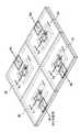
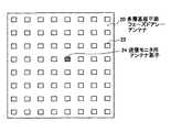
図7は、移動体SNG装置に使用する従来の平面アクティブフェーズドアレーアンテナの一例の平面図を示す。同図中、多層基板平面アクティブフェーズドアレーアンテナ20には8×8素子のパッチ22が設けられており、各パッチ22は放射アンテナ素子とモニタ用アンテナ素子が対で形成されている。図中、ハッチングで示すアレーの中心部に位置する1つのパッチのモニタ用アンテナ素子を送信モニタ用アンテナ素子として用いる。
【0007】
図8(A),(B)は、各パッチの断面図,平面図を示す。多層基板は、基板31から基板34までの4枚からなり、基板32上に送信用の放射アンテナ素子35が形成されており、放射アンテナ素子35の送信ポートはスルーホール36によって基板33,34間に形成された送信用給電線37に接続され、送信用給電線37を介して送信用コネクタに接続される。
【0008】
基板31には同じくエッチングで形成された無給電の共振パッチで構成されるモニタ用アンテナ素子38が設けてある。送信モニタ用アンテナ素子として用いるモニタ用アンテナ素子38については、同じ平面上に作成された給電線を介してモニタ用出力コネクタに接続されている。
【0009】
この構造では、モニタ用アンテナ素子を放射用素子に積層することにより小型、薄型な構成にすることができる。また、送信電波の振幅、位相を直接モニタでき、アンテナまでをループに含むフィードバック系が構成されるため、アンテナ部の特性の変化までを補償した高精度の振幅、位相の制御が可能となる。
【0010】
【発明が解決しようとする課題】
図6の従来技術では、モニタ装置はアンテナ素子11〜1nと電力増幅器31〜3nの間に取り付けられた方向性結合器111〜11nにより送信信号の抽出を行っているので、アンテナ系を含まないフィードバックループとなっており、アンテナの放射素子の影響やインピーダンス不整合による多重反射等の影響により、空間に放射された送信電波の振幅、位相を正確にモニタすることはできない。また、アンテナ素子11〜1nと電力増幅器31〜3nが一体化したアクティブフェーズドアレーアンテナに適用する場合、方向性結合器111〜11nは比較的大きいため、小型のアクティブフェーズドアレーアンテナを構成することが困難となる。さらに、この方向性結合器111〜11nをアンテナ素子11〜1nと電力増幅器31〜3nの間に挿入した場合、アクティブフェーズドアレーアンテナの特性が影響を受け、送信電波を正確にモニタすることができないという問題がある。
【0011】
図7,図8の従来技術では、モニタ用アンテナ素子38を放射アンテナ素子35の上部に積層する構造になっているため、アンテナ系を含めたモニタが行えるが、放射アンテナ素子35の上部にモニタ用アンテナ素子38が積層して形成されているため放射特性に直接影響を与えたり、隣接するアンテナ素子あるいはサブアレーからの結合により正確なモニタができないという問題がある。
【0012】
本発明は、上記の点に鑑みなされたもので、アンテナ系を含めたフィードバックループを構成でき、また、隣接するアンテナ素子あるいはサブアレーからの相互結合による影響がなく高精度なモニタが可能なアクティブフェーズドアレーアンテナを提供することを目的とする。
【0013】
【課題を解決するための手段】
請求項1に記載の発明は、電力増幅器の出力線路で励振される励振用スロットアンテナ素子を形成した下層金属板と、
前記下層金属板の上部に、複数の放射用スロットアンテナ素子をアレー状に構成した上層金属板と、
前記下層金属板と前記上層金属板との中間層に形成され前記励振用スロットアンテナ素子の上部からずらして配置されたモニタ用スロットアンテナ素子とを有し、
前記励振用スロットアンテナ素子から放射した電磁波を空間的に分配して前記複数の放射用スロットアンテナ素子及び前記モニタ用スロットアンテナ素子に電磁結合させてなるため、
アクティブフェーズドアレーアンテナに電力増幅器を一体化した構成であってもアンテナ系を含めたフィードバックループが構成でき高精度な送信電波のモニタが可能となる。また、モニタ用スロットアンテナ素子が励振用スロットアンテナ素子を形成した下層金属板と放射用スロットアンテナ素子を構成した上層金属板の間に形成されているので、隣接するアクティブフェーズドアレーアンテナまたはサブアレーからの相互結合による直接の影響がないので、高精度なモニタが可能となり、かつアクティブフェーズドアレーアンテナの放射パターンに影響を与えることもない。また、モニタ用スロットアンテナ素子は、下層金属板と上層金属板の間であれば自由に配置できるので、電磁的な結合度自由に調節してモニタすることができる。さらに、電磁結合によりモニタするため、高い周波数においても効率よく高精度な送信電波のモニタが可能となる。
【0014】
請求項2に記載の発明は、請求項1記載のアクティブフェーズドアレーアンテナにおいて、
前記モニタ用スロットアンテナ素子を形成した中間層に、前記モニタ用スロットアンテナ素子でモニタした信号の振幅、位相を検出する回路を構成してなるため、
送信電波の振幅、位相を検出する回路をアクティブアンテナ内部に構成してなるため、送信電波の振幅、位相を検出する回路を含めたアクティブフェーズドアレーアンテナを低コストで製造することができる。
【0015】
請求項3に記載の発明は、請求項1または2記載のアクティブフェーズドアレーアンテナをサブアレーとして2次元平面にアレー状に配列してなるため、
各サブアレーから放射される電波の振幅、位相を検出することができ、高精度にアンテナのビーム制御を行うことができる。
【0016】
【発明の実施の形態】
図1,図2,図3は、本発明のアクティブフェーズドアレーアンテナの第1実施例の分解斜視図、透視斜視図、断面図を示す。同図中、金属製の放射用スロットアレー板41には、複数の放射用スロット42がx方向に一定間隔で偏波方向が一致するように一線上に配列されて形成されている。即ち、各放射用スロット42はy方向に長く、x方向に短い矩形状穴である。
【0017】
また、金属ベース43には、ストリップ導体44と電力増幅器45とストリップ導体46を収納する金属溝47が設けられている。ストリップ導体44には入力信号が供給され、電力増幅器45はストリップ導体44から供給される入力信号を増幅してストリップ導体46に供給し、ストリップ導体46から励振用スロット49に給電する。金属ベース43の上面は金属製の励振用スロット板48で覆われ、この励振用スロット板48に放射用スロット42を励振するための励振用スロット49が形成されている。励振用スロット49はy方向に長く、x方向に短い矩形状穴である。
【0018】
放射用スロットアレー板41と金属ベース43の間には、誘電体基板51が配置され、誘電体基板51の上面には矩形状の金属膜によってモニタ用アンテナ素子52が形成されており、誘電体基板51とこれに支持されるモニタ用アンテナ素子52とで送信電波モニタ用素子53を構成している。ここで、モニタ用アンテナ素子52は励振用スロット49の上部に積層するのではなく、例えばy方向にずらして配置されている。
【0019】
ストリップ導体44と金属ベース43と励振用スロット板48により入力用トリプレート線路54が構成され、ストリップ導体46と金属ベース43と励振用スロット板48により出力用トリプレート線路55が構成されている。そして、入力用トリプレート線路54と、出力用トリプレート線路55と、電力増幅器45と、金属ベース43と、励振用スロット49が形成されている励振用スロット板48とにより、1素子の励振用アクティブフェーズドアレーアンテナが構成されている。
【0020】
ここで、信号の流れを説明する。入力端子T1からストリップ導体44に入力された高周波信号は入力用トリプレート線路54を伝送されて電力増幅器45に入力される。電力増幅器45で電力増幅されて出力される信号は出力用トリプレート線路55を伝送されて励振用スロット板48上に形成されている励振用スロット49に電磁結合する。電磁結合した高周波信号は励振用スロット49から放射され、放射用スロットアレー板41上に形成されている複数の放射用スロット42に電磁結合して空間的に分配され、複数の放射用スロット42から空間に放射される。
【0021】
また、励振用スロット49から放射された高周波信号の一部は放射用スロットアレー板41と金属ベース43の間に配置された送信電波モニタ用素子53のモニタ用アンテナ素子52を電磁結合により励振し、モニタ用アンテナ素子52に接続されたモニタ出力端子R1から出力される。
【0022】
本実施例では、電力増幅器45の出力線路であるストリップ導体46で励振される励振用スロット49を形成した励振用スロット板48の上部に、複数の放射用スロット42をアレー状に構成した放射用スロットアレー板41を配置した構造において、下層側の励振用スロット49から放射した電磁波を空間的に分配して上層側の放射用スロット42に適当な結合度で電磁結合させ、上層側と下層側の中間層に励振用スロット49の上部からずらした位置にモニタ用アンテナ素子52を形成することにより、アクティブフェーズドアレーアンテナと電力増幅器45を一体化した構成であってもアンテナ系を含めたフィードバックループが構成できるので高精度な送信電波のモニタが可能となる。
【0023】
また、モニタ用アンテナ素子52は、放射用スロット42が形成されている放射用スロットアレー板41と励振用スロット49が形成されている励振用スロット板48の間に励振用スロット49の上部からずらして配置されているので、隣接するアクティブアンテナまたはサブアレーからの相互結合による直接の影響がないので、高精度なモニタが可能となり、かつアレーアンテナの放射パターンに影響を与えることもない。
【0024】
また、モニタ用アンテナ素子52及び送信電波の振幅、位相を検出する送信電波モニタ回路をアクティブアンテナ内部に簡単に構成できるため、送信電波モニタ回路を含めたアクティブフェーズドアレーアンテナを低コストで製造することができる。
【0025】
また、モニタ用アンテナ素子52は、放射用スロット42が形成されている放射用スロットアレー板41と励振用スロット49が形成されている励振用スロット板48の間であれば自由に配置できるので、電磁的な結合度自由に調節してモニタすることができる。さらに、電磁結合によりモニタするため、高い周波数においても効率よく高精度な送信電波のモニタが可能となる。
【0026】
図4,図5は、本発明のアクティブフェーズドアレーアンテナの第2実施例の透視斜視図、断面図を示す。このアクティブフェーズドアレーアンテナの構造は、図1〜図3に示すアクティブフェーズドアレーアンテナをサブアレーとし、4個のサブアレー60,61,62,63を2次元平面にアレー状に配列しアクティブフェーズドアレーアンテナを構成したものである。なお、上記サブアレーは4個配列したものに限らず、例えば縦横それぞれ数10から数100個をアレー状に配列する構成であっても良い。
【0027】
図4,図5において、4個のサブアレー60,61,62,63それぞれは、入力端子T1,T2,T3,T4から各サブアレーのストリップ導体44に高周波信号を入力され、この高周波信号は入力用トリプレート線路54を伝送されて電力増幅器45に入力される。電力増幅器45で電力増幅されて出力される信号は出力用トリプレート線路55を伝送されて励振用スロット板48上に形成されている励振用スロット49に電磁結合する。電磁結合した高周波信号は励振用スロット49から放射され、放射用スロットアレー板41上に形成されている複数の放射用スロット42に電磁結合して空間的に分配され、各サブアレーの複数の放射用スロット42から空間に放射される。
【0028】
また、各サブアレーの励振用スロット49から放射された高周波信号の一部は放射用スロットアレー板41と金属ベース43の間に配置された送信電波モニタ用素子53のモニタ用アンテナ素子52を電磁結合により励振し、モニタ用アンテナ素子52に接続された各サブアレーのモニタ出力端子R1,R2,R3,R4から出力される。従って、モニタ出力端子R1,R2,R3,R4にて各サブアレーから放射される電波の振幅、位相を検出することができ、高精度にアンテナのビーム制御を行うことができる。
【0029】
なお、上記実施例ではモニタ用アンテナ素子52の形状を平面構造としているが、同軸線路などの立体回路で構成しても良い。また、モニタ用アンテナ素子52が形成された誘電体基板51上に送信電波の振幅、位相を検出する送信電波モニタ回路を集積化することもできるので、送信電波モニタ回路を内蔵したアクティブフェーズドアレーアンテナの構造をさらに小型、薄型化することができ、移動体SNG装置や衛星搭載用などに使用されるアクティブフェーズドアレーアンテナで高精度なビーム形成を行うことが可能となる。
【0030】
なお、励振用スロット49が請求項記載の励振用スロットアンテナ素子に対応し、励振用スロット板48が下層金属板に対応し、放射用スロット42が放射用スロットアンテナ素子に対応し、放射用スロットアレー板41が上層金属板に対応し、モニタ用アンテナ素子52がモニタ用スロットアンテナ素子に対応する。
【0031】
【発明の効果】
上述の如く、求項1に記載の発明は、アクティブフェーズドアレーアンテナに電力増幅器を一体化した構成であってもアンテナ系を含めたフィードバックループが構成でき高精度な送信電波のモニタが可能となる。また、モニタ用スロットアンテナ素子が励振用スロットアンテナ素子を形成した下層金属板と放射用スロットアンテナ素子を構成した上層金属板の間に形成されているので、隣接するアクティブフェーズドアレーアンテナまたはサブアレーからの相互結合による直接の影響がないので、高精度なモニタが可能となり、かつアクティブフェーズドアレーアンテナの放射パターンに影響を与えることもない。また、モニタ用スロットアンテナ素子は、下層金属板と上層金属板の間であれば自由に配置できるので、電磁的な結合度自由に調節してモニタすることができる。さらに、電磁結合によりモニタするため、高い周波数においても効率よく高精度な送信電波のモニタが可能となる。
【0032】
請求項2に記載の発明は、送信電波の振幅、位相を検出する回路をアクティブアンテナ内部に構成してなるため、送信電波の振幅、位相を検出する回路を含めたアクティブフェーズドアレーアンテナを低コストで製造することができる。
【0033】
請求項3に記載の発明は、各サブアレーから放射される電波の振幅、位相を検出することができ、高精度にアンテナのビーム制御を行うことができる。
【図面の簡単な説明】
【図1】本発明のアクティブフェーズドアレーアンテナの第1実施例の分解斜視図である。
【図2】本発明のアクティブフェーズドアレーアンテナの第1実施例の透視斜視図である。
【図3】本発明のアクティブフェーズドアレーアンテナの第1実施例の断面図である。
【図4】本発明のアクティブフェーズドアレーアンテナの第2実施例の透視斜視図である。
【図5】本発明のアクティブフェーズドアレーアンテナの第2実施例の断面図である。
【図6】従来のアクティブフェーズドアレーアンテナの一例の回路構成図である。
【図7】従来の平面アクティブフェーズドアレーアンテナの一例の平面図である。
【図8】パッチの断面図,平面図である。
【符号の説明】
41 放射用スロットアレー板
42 放射用スロット
43 金属ベース
44 ストリップ導体
45 電力増幅器
46 ストリップ導体
47 金属溝
48 励振用スロット板
49 励振用スロット
51 誘電体基板
52 モニタ用アンテナ素子
53 送信電波モニタ用素子
54 入力用トリプレート線路
55 出力用トリプレート線路
60,61,62,63 サブアレー[0001]
BACKGROUND OF THE INVENTION
The present invention relates to an active phased array antenna and a transmission apparatus using the same, and more particularly to an active phased array antenna in which an antenna element and a semiconductor device are integrated and a transmission apparatus using the same.
[0002]
[Prior art]
In recent years, as an antenna of a mobile SNG (news material transmission) device that has an electronic tracking function and transmits information from a mobile body, a satellite broadcast receiving antenna capable of scanning multiple beams and spatially, or a transmitting and receiving antenna mounted on a satellite An active phased array antenna has been developed.
[0003]
FIG. 6 shows a circuit configuration diagram of an example of a conventional active phased array antenna used in a radar apparatus. In the figure, the transmission pulse signal transmitted from the transmitter 7 is supplied to the power distributor 9 via the
[0004]
Reflected waves of the transmission pulse signal reflected by the observation target are received by the antenna elements 11 to 1n . Received signal received by the antenna element 11 to 1n, the received signal input is led to the low-noise amplifier 51 to 5n via the first circulator 21 to 2n are amplified second circulator It is output to the phase shifters 61 to 6n via 41 to 4n . The phase shifters 61 to 6n control the input received signal to a predetermined phase and supply it to the power distributor 9. The power distributor 9 synthesizes the received reception signals and outputs them to the
[0005]
Directional couplers 111 to 11n are provided at the output ends of the plurality of power amplifiers 31 to 3n , respectively, and a part of the output of the power amplifiers 31 to 3n is provided by the directional couplers 111 to 11n. This is extracted as a monitor signal, and this monitor signal is detected by the detectors 121 to 12n and output by a monitor device (not shown) to detect the operating states of the plurality of power amplifiers 31 to 3n . Thereby, the amplitude and phase of the radio wave radiated from each of the antenna elements 11 to 1n can be obtained, and the antenna beam can be scanned in a desired direction with high accuracy.
[0006]
FIG. 7 shows a plan view of an example of a conventional planar active phased array antenna used in a mobile SNG apparatus. In the figure, a multi-layer substrate planar active phased array antenna 20 is provided with
[0007]
8A and 8B are a cross-sectional view and a plan view of each patch. The multilayer substrate is composed of four substrates from
[0008]
The
[0009]
In this structure, the monitor antenna element can be stacked on the radiating element to make the structure small and thin. In addition, since the amplitude and phase of the transmission radio wave can be directly monitored and a feedback system including the loop up to the antenna is configured, it is possible to control the amplitude and phase with high accuracy that compensates for changes in the characteristics of the antenna unit.
[0010]
[Problems to be solved by the invention]
In the prior art of FIG. 6, the monitor device extracts transmission signals by directional couplers 111 to 11n attached between the antenna elements 11 to 1n and the power amplifiers 31 to 3n . The feedback loop does not include the antenna system, and the amplitude and phase of the transmitted radio wave radiated into the space cannot be accurately monitored due to the influence of the radiating element of the antenna or the influence of multiple reflection due to impedance mismatching. . Further, when applied to an active phased array antenna in which the antenna elements 11 to 1n and the power amplifiers 31 to 3n are integrated, the directional couplers 111 to 11n are relatively large, and thus a small active phased array. It becomes difficult to configure the antenna. Further, when the directional couplers 111 to 11n are inserted between the antenna elements 11 to 1n and the power amplifiers 31 to 3n , the characteristics of the active phased array antenna are affected, and the transmitted radio wave is accurately There is a problem that cannot be monitored.
[0011]
7 and 8, since the monitor antenna element 38 is stacked on the radiation antenna element 35, monitoring including the antenna system can be performed. Since the antenna elements 38 are laminated, there is a problem in that radiation characteristics are directly affected, and accurate monitoring cannot be performed due to coupling from adjacent antenna elements or subarrays.
[0012]
The present invention has been made in view of the above points, and is capable of forming a feedback loop including an antenna system, and is not affected by mutual coupling from adjacent antenna elements or subarrays. An object is to provide an array antenna.
[0013]
[Means for Solving the Problems]
The invention according to claim 1 is a lower metal plate on which an excitation slot antenna element excited by an output line of a power amplifier is formed,
An upper metal plate in which a plurality of slot antenna elements for radiation are configured in an array on the lower metal plate,
A monitor slot antenna element formed in an intermediate layer between the lower metal plate and the upper metal plate and arranged to be shifted from the upper part of the excitation slot antenna element;
Since the electromagnetic waves radiated from the excitation slot antenna elements are spatially distributed and electromagnetically coupled to the plurality of radiating slot antenna elements and the monitor slot antenna elements,
Even with a configuration in which a power amplifier is integrated with an active phased array antenna, a feedback loop including the antenna system can be configured, and high-accuracy transmission radio waves can be monitored. Further, since the monitor slot antenna element is formed between the lower metal plate forming the excitation slot antenna element and the upper metal plate constituting the radiating slot antenna element, mutual coupling from the adjacent active phased array antenna or sub-array Therefore, it is possible to monitor with high accuracy and does not affect the radiation pattern of the active phased array antenna. Further, since the slot antenna element for monitoring can be freely arranged between the lower metal plate and the upper metal plate, it can be monitored by freely adjusting the electromagnetic coupling degree. Furthermore, since monitoring is performed by electromagnetic coupling, it is possible to monitor transmission radio waves efficiently and accurately even at high frequencies.
[0014]
The invention according to claim 2 is the active phased array antenna according to claim 1,
Since the intermediate layer in which the monitoring slot antenna element is formed constitutes a circuit for detecting the amplitude and phase of the signal monitored by the monitoring slot antenna element,
Since the circuit for detecting the amplitude and phase of the transmission radio wave is configured inside the active antenna, an active phased array antenna including a circuit for detecting the amplitude and phase of the transmission radio wave can be manufactured at low cost.
[0015]
Since the invention according to claim 3 is formed by arranging the active phased array antenna according to claim 1 or 2 as a sub-array in a two-dimensional plane,
The amplitude and phase of the radio wave radiated from each subarray can be detected, and the beam control of the antenna can be performed with high accuracy.
[0016]
DETAILED DESCRIPTION OF THE INVENTION
1, 2 and 3 are an exploded perspective view, a perspective view and a sectional view of a first embodiment of the active phased array antenna of the present invention. In the figure, a metal radiating
[0017]
The
[0018]
A
[0019]
The
[0020]
Here, the flow of signals will be described. The high-frequency signal input from the input terminal T 1 to the
[0021]
A part of the high-frequency signal radiated from the
[0022]
In this embodiment, a plurality of radiating
[0023]
The
[0024]
In addition, since the
[0025]
The
[0026]
4 and 5 are a perspective view and a sectional view of a second embodiment of the active phased array antenna of the present invention. The active phased array antenna has a structure in which the active phased array antenna shown in FIGS. 1 to 3 is a subarray, and four
[0027]
4 and 5, each of the four
[0028]
Further, a part of the high frequency signal radiated from the
[0029]
In the above embodiment, the shape of the
[0030]
The
[0031]
【The invention's effect】
As described above, the invention described in claim 1 can form a feedback loop including an antenna system even when the power amplifier is integrated with the active phased array antenna and can monitor the transmission radio wave with high accuracy. . Further, since the monitor slot antenna element is formed between the lower metal plate forming the excitation slot antenna element and the upper metal plate constituting the radiating slot antenna element, mutual coupling from the adjacent active phased array antenna or sub-array Therefore, it is possible to monitor with high accuracy and does not affect the radiation pattern of the active phased array antenna. Further, since the slot antenna element for monitoring can be freely arranged between the lower metal plate and the upper metal plate, it can be monitored by freely adjusting the electromagnetic coupling degree. Furthermore, since monitoring is performed by electromagnetic coupling, it is possible to monitor transmission radio waves efficiently and accurately even at high frequencies.
[0032]
Since the circuit for detecting the amplitude and phase of the transmission radio wave is configured inside the active antenna, the active phased array antenna including the circuit for detecting the amplitude and phase of the transmission radio wave is reduced in cost. Can be manufactured.
[0033]
The invention according to claim 3 can detect the amplitude and phase of the radio wave radiated from each sub-array, and can perform beam control of the antenna with high accuracy.
[Brief description of the drawings]
FIG. 1 is an exploded perspective view of a first embodiment of an active phased array antenna of the present invention.
FIG. 2 is a perspective view of the first embodiment of the active phased array antenna of the present invention.
FIG. 3 is a cross-sectional view of a first embodiment of an active phased array antenna of the present invention.
FIG. 4 is a perspective view of a second embodiment of the active phased array antenna of the present invention.
FIG. 5 is a cross-sectional view of a second embodiment of an active phased array antenna of the present invention.
FIG. 6 is a circuit configuration diagram of an example of a conventional active phased array antenna.
FIG. 7 is a plan view of an example of a conventional planar active phased array antenna.
FIG. 8 is a cross-sectional view and a plan view of a patch.
[Explanation of symbols]
41 Radiation
Claims (4)
Translated fromJapanese電力増幅器の出力線路で励振される励振用スロットアンテナ素子を形成した下層金属板と、
前記下層金属板の上部に、複数の放射用スロットアンテナ素子をアレー状に構成した上層金属板と、
前記下層金属板と前記上層金属板との中間層に形成され前記励振用スロットアンテナ素子の上部からずらして配置されたモニタ用スロットアンテナ素子とを有し、
前記励振用スロットアンテナ素子から放射した電磁波を空間的に分配して前記複数の放射用スロットアンテナ素子及び前記モニタ用スロットアンテナ素子に電磁結合させてなることを特徴とするアクティブフェーズドアレーアンテナ。In active phased array antenna with integrated power amplifier,
A lower metal plate on which a slot antenna element for excitation excited by an output line of a power amplifier is formed;
An upper metal plate in which a plurality of slot antenna elements for radiation are configured in an array on the lower metal plate,
A monitor slot antenna element formed in an intermediate layer between the lower metal plate and the upper metal plate and arranged to be shifted from the upper part of the excitation slot antenna element;
An active phased array antenna, wherein electromagnetic waves radiated from the exciting slot antenna elements are spatially distributed and electromagnetically coupled to the plurality of radiating slot antenna elements and the monitoring slot antenna elements.
前記モニタ用スロットアンテナ素子を形成した中間層に、前記モニタ用スロットアンテナ素子でモニタした信号の振幅、位相を検出する回路を構成してなることを特徴とするアクティブフェーズドアレーアンテナ。The active phased array antenna according to claim 1,
An active phased array antenna comprising a circuit for detecting an amplitude and a phase of a signal monitored by the monitoring slot antenna element in an intermediate layer in which the monitoring slot antenna element is formed.
Priority Applications (1)
| Application Number | Priority Date | Filing Date | Title |
|---|---|---|---|
| JP2001218324AJP4022052B2 (en) | 2001-07-18 | 2001-07-18 | Active phased array antenna and transmitter using the same |
Applications Claiming Priority (1)
| Application Number | Priority Date | Filing Date | Title |
|---|---|---|---|
| JP2001218324AJP4022052B2 (en) | 2001-07-18 | 2001-07-18 | Active phased array antenna and transmitter using the same |
Publications (2)
| Publication Number | Publication Date |
|---|---|
| JP2003032033A JP2003032033A (en) | 2003-01-31 |
| JP4022052B2true JP4022052B2 (en) | 2007-12-12 |
Family
ID=19052516
Family Applications (1)
| Application Number | Title | Priority Date | Filing Date |
|---|---|---|---|
| JP2001218324AExpired - LifetimeJP4022052B2 (en) | 2001-07-18 | 2001-07-18 | Active phased array antenna and transmitter using the same |
Country Status (1)
| Country | Link |
|---|---|
| JP (1) | JP4022052B2 (en) |
Families Citing this family (8)
| Publication number | Priority date | Publication date | Assignee | Title |
|---|---|---|---|---|
| JP4227589B2 (en)* | 2004-12-03 | 2009-02-18 | 日本放送協会 | Active array antenna |
| CN105305189B (en)* | 2015-11-18 | 2018-07-06 | 成都雷电微力科技有限公司 | A kind of molding of wave control more than one point cable |
| CN105305118B (en)* | 2015-11-18 | 2018-11-06 | 成都雷电微力科技有限公司 | A kind of active phase array antenna beam controlling system |
| CN106154603B (en)* | 2016-07-29 | 2019-12-06 | 合肥工业大学 | Liquid crystal phase-shifting unit and phase-controlled antenna formed by same |
| FR3062525B1 (en)* | 2017-02-01 | 2020-11-20 | Inst Vedecom | SLOTTED ANTENNA INTEGRATED IN A PRINTED CIRCUIT BOARD AND METHOD OF MANUFACTURING THE SAME |
| CN111751795B (en)* | 2020-06-12 | 2024-09-24 | 中国船舶集团有限公司第七二四研究所 | Monitoring device for microstrip antenna with dielectric fin line |
| CN113437501B (en)* | 2021-04-27 | 2023-02-14 | 中国电子科技集团公司第十四研究所 | A Miniaturized Highly Integrated Antenna Interface Module |
| CN113126074B (en)* | 2021-04-28 | 2025-01-07 | 西安天安电子科技有限公司 | X-band highly integrated two-dimensional phased array radar RF front end |
Family Cites Families (5)
| Publication number | Priority date | Publication date | Assignee | Title |
|---|---|---|---|---|
| JPS5612104A (en)* | 1979-07-12 | 1981-02-06 | Toshiba Corp | Radar unit |
| JP3618858B2 (en)* | 1995-10-30 | 2005-02-09 | 日本放送協会 | Mobile SNG device |
| JP2000078072A (en)* | 1998-08-28 | 2000-03-14 | Hitachi Ltd | Transceiver |
| JP2000261239A (en)* | 1999-03-05 | 2000-09-22 | Fujitsu Ltd | Waveguide slot antenna |
| JP2001177332A (en)* | 1999-12-17 | 2001-06-29 | Matsushita Electric Works Ltd | Radar system |
- 2001
- 2001-07-18JPJP2001218324Apatent/JP4022052B2/ennot_activeExpired - Lifetime
Also Published As
| Publication number | Publication date |
|---|---|
| JP2003032033A (en) | 2003-01-31 |
Similar Documents
| Publication | Publication Date | Title |
|---|---|---|
| US12255406B2 (en) | System and method for over-the-air antenna calibration | |
| US8723727B2 (en) | Slot antenna and RFID method | |
| CN107078403B (en) | Wireless communication module | |
| JP5469061B2 (en) | Improvements on reconfigurable antennas | |
| US6538603B1 (en) | Phased array antennas incorporating voltage-tunable phase shifters | |
| KR101174637B1 (en) | Active phased array antenna and active phased array ladar having the same | |
| CN106450782B (en) | Radar component | |
| US20060279465A1 (en) | Plate board type MIMO array antenna including isolation element | |
| US20050237258A1 (en) | Switched multi-beam antenna | |
| KR20010039531A (en) | Steerable-beam multiple-feed dielectric resonator antenna | |
| CN111755819B (en) | Inverted microstrip traveling wave patch array antenna system | |
| KR20060041826A (en) | Circular polarization array antenna | |
| JPH06232621A (en) | Active transmission phased array antenna | |
| CN111755832B (en) | Integrated back cavity slot array antenna system | |
| JPH034604A (en) | Light-weight low-profile phased array antenna with electromagnetically coupled integrated sub-array | |
| CN112313836A (en) | Millimeter wave antenna, antenna assembly, millimeter wave radar system and movable platform | |
| JP4022052B2 (en) | Active phased array antenna and transmitter using the same | |
| US9059503B2 (en) | Antenna arrangement for transmitting signals | |
| JPH04122107A (en) | microstrip antenna | |
| KR102218965B1 (en) | Microstrip array antenna and radar device comprising the same | |
| JP3782278B2 (en) | Beam width control method of dual-polarized antenna | |
| JP5972215B2 (en) | Improvements on reconfigurable antennas | |
| US6943735B1 (en) | Antenna with layered ground plane | |
| US11482794B1 (en) | Slot-fed unit cell and current sheet array | |
| Numan et al. | Wide field of view retrodirective millimeter wave antenna array with pulse modulation and orthogonal polarization states |
Legal Events
| Date | Code | Title | Description |
|---|---|---|---|
| A621 | Written request for application examination | Free format text:JAPANESE INTERMEDIATE CODE: A621 Effective date:20060327 | |
| A977 | Report on retrieval | Free format text:JAPANESE INTERMEDIATE CODE: A971007 Effective date:20070822 | |
| TRDD | Decision of grant or rejection written | ||
| A01 | Written decision to grant a patent or to grant a registration (utility model) | Free format text:JAPANESE INTERMEDIATE CODE: A01 Effective date:20070925 | |
| A61 | First payment of annual fees (during grant procedure) | Free format text:JAPANESE INTERMEDIATE CODE: A61 Effective date:20070928 | |
| FPAY | Renewal fee payment (prs date is renewal date of database) | Free format text:PAYMENT UNTIL: 20101005 Year of fee payment:3 | |
| R150 | Certificate of patent (=grant) or registration of utility model | Free format text:JAPANESE INTERMEDIATE CODE: R150 | |
| FPAY | Renewal fee payment (prs date is renewal date of database) | Free format text:PAYMENT UNTIL: 20111005 Year of fee payment:4 | |
| FPAY | Renewal fee payment (prs date is renewal date of database) | Free format text:PAYMENT UNTIL: 20121005 Year of fee payment:5 |