JP4012393B2 - Storage device, internal control method and system for storage device, and control method for storage means in system - Google Patents
Storage device, internal control method and system for storage device, and control method for storage means in systemDownload PDFInfo
- Publication number
- JP4012393B2 JP4012393B2JP2001345266AJP2001345266AJP4012393B2JP 4012393 B2JP4012393 B2JP 4012393B2JP 2001345266 AJP2001345266 AJP 2001345266AJP 2001345266 AJP2001345266 AJP 2001345266AJP 4012393 B2JP4012393 B2JP 4012393B2
- Authority
- JP
- Japan
- Prior art keywords
- address
- bits
- bit
- command
- latency
- Prior art date
- Legal status (The legal status is an assumption and is not a legal conclusion. Google has not performed a legal analysis and makes no representation as to the accuracy of the status listed.)
- Expired - Fee Related
Links
Images


Landscapes
- Dram (AREA)
Description
Translated fromJapanese【0001】
【発明の属する技術分野】
本発明は、記憶装置、記憶装置の内部制御方法、システム、及びシステムにおける記憶手段の制御方法に関するものである。
【0002】
近年、データ保持動作が随時必要な半導体メモリ(ダイナミックRAM:Dynamic RAM)は、顧客(システム側)から要求される記憶容量の増大、アクセス高速化(動作周波数の高周波化)、I/Oバス幅の拡張(1アクセスでデータを扱うビット数幅の増大)などにより、消費電流が増大する傾向にある。これに伴い、メモリデバイスを搭載したシステム機器全体の消費電流も増加する傾向となっており、顧客からメモリデバイスの消費電力削減が求められている。
【0003】
また、前述の消費電流の増大は、メモリデバイスのチップ温度上昇を招く場合がある。一般に、DRAMセルのデータ保持特性(≒ Refresh特性:TREF)は高温で悪化する(保持時間が短くなる)ので、この理由からも消費電流の削減が求められる。
【0004】
従って、半導体メモリは、記憶容量の増大やアクセスの高速化、I/Oバス幅の拡張などの性能の向上と、消費電力の削減が同時に求められている。
【0005】
【従来の技術】
メモリデバイスは、複数のメモリセルがアレイ配置されたメモリセルアレイとセンスアンプを有している。各メモリセルはワード線とビット線に接続され、センスアンプはビット線に接続されている。センスアンプはビット線と対であり、1つのセルの情報(リードデータ)の増幅と保持を行う。
【0006】
メモリセルアレイは行アドレスによりワード線が展開されるX展開方向と、列アドレスによりビット線とセンスアンプが展開されるY展開方向とにアレイ展開される。1Mビットのメモリ容量であれば、一例としてメモリデバイスの論理アドレスは、10ビット(210=1024本のワード線:WL)のXアドレス(Row Address )を、10ビット(210=1024本のビット線:BL(1024個のセンスアンプ))のYアドレス(Column Address)から構成することができる(注:ビット線定義=一対の相補ビット線)。このとき、仮にワード線とビット線の配線ピッチが同じであれば、論理的なメモリアレイは正方形にイメージされる。
【0007】
メモリデバイスの内部動作を、システムクロックCLKに対して同期型であるSDRAM(Synchronous DRAM)を例にして説明する。
SDRAMは、制御コマンドとしてメモリデバイスが活性/非活性するためのシステムクロックCLKに同期したアクティブ/プリチャージコマンド(非同期型のメモリデバイスではチップイネーブル信号/CE(”/”はバーを示す)の立下りと立上り)と、メモリデバイスにデータを入出力する為のリード/ライトコマンドにより動作する。
【0008】
システムクロックCLKの立上りエッジに於いてアクティブコマンドを外部印加されると、Xアドレスを取り込みXデコーダでデコードして一本のワード線を選択し、それを活性化させる。選択されたワード線に接続されたそれぞれのメモリセルがそれぞれのビット線にデータを出力し、それぞれのセンスアンプがデータを増幅し保持(データのラッチ)する。
【0009】
その後、システムクロックCLKの立上りエッジに於いて(アクティブコマンドから数CLK遅れで)リードコマンドを外部印加されると、Yアドレスを取り込みYデコーダでデコードして一つのセンスアンプの保持されたデータをメモリデバイス外部に出力する。また、ライトコマンドを外部印加されると、Yアドレスを取り込みYデコーダでデコードして(ライトコマンド印加時に入力された)書込みデータを一つのセンスアンプを介してメモリセルに書き込む。その後、更に必要に応じてリード/ライトコマンドを随時行ない、希望のYアドレスに応じたメモリセルと外部とのアクセスを行なう。
【0010】
リード/ライトコマンドが終了した後は、システムクロックCLKの立上りエッジに於いて(リード/ライトコマンドから数CLK遅れで)プリチャージコマンドを印加して、活性化されたワード線とセンスアンプとビット線をリセット(イコライズ)してメモリアレイは初期状態(次のアクティブコマンドに備える)に戻る。
【0011】
リセット動作までは内部時間が掛かり、プリチャージコマンドから次のアクティブコマンドを印加するには数CLKの猶予(待ち)が必要である。同様に、アクティブコマンドからリード/ライトコマンドまで数CLKの猶予(待ち)が必要である。
【0012】
尚、ここでは説明の簡素化の為にメモリアレイの入出力ビット数が1の場合で説明したが、入出力のビット数がn(nI/Oと記す(ex.4I/O))の場合には、Yアドレスによって同時にn個のセンスアンプが選択される。そして、各センスアンプはそれぞれn個のI/Oバスを介してそれぞれn個のI/Oポートに接続される。
【0013】
Yアドレスの深さは、ページ長と呼ばれる。メモリデバイスは、1回のアクティブコマンドに応答し、少なくともI/Oバス幅×ページ長の数のセンスアンプを動作させる。例えば、Yアドレスが8ビット(YA<0:7> )に設定されたSDRAMの場合、ページ長は256である。このSDRAMが32ビットのI/Oバス幅を持つ場合、アクティブコマンドに応答して少なくとも8,192(=256×32)個のセンスアンプが動作する。
【0014】
SDRAMは、随時入力されるリードコマンドによりアクティブコマンドで選択したワード線に接続された複数のメモリセルの情報を複数のセンスアンプにそれぞれラッチする。従って、1本のワード線を活性化すれば、ページ長分のメモリセルの情報を適宜外部に読み出すことができる。詳述すると、随時入力されるリード/ライトコマンド毎に該コマンドと同時に入力されるYアドレスによりYデコーダで随時センスアンプを選択することで、任意のYアドレスのメモリセルから情報を読み出す。即ち、Xアドレスは固定したままYアドレスをランダムにアクセスすることができる。このような動作をYアドレス優先動作と呼ぶ。尚、ライトコマンドに対しても同様に任意のYアドレスのメモリセルに情報を書き込むことができる。
【0015】
このYアドレス優先動作では、ランダムアクセスの優位性に加えて、一回のアクティブコマンドにより動作するセンスアンプ群のそれぞれのセンスアンプにラッチした複数のデータを効率的に利用することができる。つまり、一回のワード線の充放電電流と一回の(複数)センスアンプによる(複数)ビット線充放電電流により、256ページに含まれるメモリセルに対してランダムなアクセスが可能となる。
【0016】
故に、1回のアクセスに要する消費電流は、同じ時に活性化されるページ内へのアクセス回数でワード線の充放電とビット線の充放電による消費電流を割った値となる。従って、同時に活性化されるページ内のアクセス回数が多いほど、SDRAMのアクセス回数あたりの消費電流は少なくなる。
【0017】
更に、Yアドレス優先動作では、アクティブコマンドからリード/ライトコマンドを印加するまでに必要なクロック数と、プリチャージコマンドから次のアクティブコマンドを印加するまでに必要なクロック数は、動作全体に占める割合が少ない。従って、入出力バスをデータが占有する割合(データ占有率)が高く、システムにおいてI/Oバスの効率がよい。これらは、システムクロックの周波数が高くなる(高周波になる)ほど、レイテンシを大きくとらなければならないSDRAMでは入出力バスのデータ占有率が高くできるという効果がある。
【0018】
【発明が解決しようとする課題】
ところで、SDRAMを使用する顧客のシステムによっては、アクセスするビット長が少ない(例えば連続した4ビット、8ビットなど)ものがある。このようなシステムによるSDRAMのアクセスは、1回のアクティブコマンドからプリチャージコマンドの間に、ページ長より少ない数のリード/ライト動作しかせず、次のアクティブコマンドによりXアドレスが変更される。このような動作を、便宜的にXアドレス優先動作と呼ぶ。この動作では、1回のアクティブコマンドにより活性化されるセンスアンプが効率的に使用されていない。
【0019】
例えば、Yアドレスを変更(Xアドレスは一定)して4つのメモリセルに対してアクセスする。この場合、Xアドレスにより選択される1本のワード線の充放電電流と、活性化するセンスアンプの数(8192個)(センスアンプによるビット線の充放電電流を含む)に対応する電流を消費する。このときの消費電流をP(y)とする。従って1つのメモリセルに対するアクセスの消費電流は、P(y)/4となる。
【0020】
一方、Xアドレスを変更(Yアドレスは任意)して4つのメモリセルをアクセスする場合、Xアドレスを変更する毎にアクティブコマンドとプリチャージコマンドを必要とする。従って、このアクセス方法の場合、Xアドレスを固定してアクセスするときの4倍(4×P(y))の消費電流となり、1つのメモリセルに対するアクセスの消費電流はP(y)となる。
【0021】
従って、Xアドレス優先動作を多用するシステムやアプリケーションの場合、Yアドレスが浅く(ページ数が少なく)Xアドレスが深いメモリデバイスが有効である。
【0022】
しかし、メモリデバイスを使用するシステムのアクセス方法、アプリケーションのステップによりXアドレス優先動作とYアドレス優先動作が混在する場合がある。このような場合、Yアドレスが浅いメモリデバイスを使用すると、アクセスの順序によってアクセス速度が極めて遅くなる場合があり、速度向上の妨げとなる。一方、Xアドレスが浅いメモリデバイスを使用すると、消費電流低減の妨げとなる。
【0023】
また、このようなXアドレス、Yアドレスの深さが異なるメモリデバイスは標準品とピン配列やパッケージの大きさが異なり、メモリデバイスを単純に置き換えすることができない。このため、メモリデバイスを実装する基板等を作成しなおさなければならずコストの増加や開発期間の長期化を招いていた。
【0024】
更に、Xアドレス優先動作のような消費電流の大きい動作を繰り返すと、メモリデバイスのチップの温度(ジャンクション温度)を上昇させることがある。この場合、温度上昇によってデータ保持特性が悪化し、データ保持動作であるリフレッシュ動作を頻繁に行なわなければならなくなる。すると、メモリデバイスへのアクセスによる温度上昇にメモリデバイスのリフレッシュ動作による自己発熱を加えたチップ温度となり、データ保持特性の悪化と頻繁なリフレッシュ動作による消費電流の更なる増大を招く。また、データ保持動作を顧客システム側の制御に関係なく非同期で行なう場合(セルフリフレッシュ動作)には、これらリフレッシュ動作における外部からのアクセスに応答しないビジー状態が増加することになり、システムのパフォーマンスが低下(I/Oバスのデータ占有率の低下)する。
【0025】
本発明は上記問題点を解決するためになされたものであって、その目的はパッケージを変更することなく効率的なアクセスと消費電流の低減を図ることのできる記憶装置、記憶装置の内部制御方法、システム、及びシステムにおける記憶手段の制御方法を提供することにある。
【0026】
【課題を解決するための手段】
請求項1に記載の発明によれば、所定数のアドレス端子を用いてMビットの第1アドレスと該Mビットよりも少ないNビットの第2アドレスとを取り込み、メモリセルがアレイ配列されたメモリセルアレイをアクセスする記憶装置において、前記メモリセルアレイの論理アドレスマップ形状を、アクセス形態情報に基づいて、前記所定数のアドレス端子よりもiビット多い(M+i)ビットの第1アドレスと前記Nビットよりもiビット少ない(N−i)ビットの第2アドレスとで表される論理アドレスマップ形状に変更し、該変更に伴い増加した前記iビットの第1アドレスを、前記Mビットの第1アドレスを発生させた後に時分割で発生させるアドレス制御手段を備え、前記アドレス制御手段は、前記(N−i)ビットの第2アドレスに対応する第1リードコマンドの発行から第1データ出力までの第1レイテンシが、前記(N−i)ビットの第2アドレスに対応する第2リードコマンドの発行から第2データ出力までの第2レイテンシよりも長くなるように、前記増加したiビットの第1アドレスを取り込む。
請求項2に記載の発明によれば、前記アドレス制御手段は、アクティブコマンドの発行後に発行される前記第1リードコマンドに伴って、前記増加したiビットの第1アドレスを取り込む。
請求項3に記載の発明によれば、前記第1アドレスはロウアドレスであり、前記第2アドレスはコラムアドレスである。
請求項4に記載の発明によれば、前記第2レイテンシは、モードレジスタに設定されている。
請求項5に記載の発明によれば、前記増加はページ長変化に伴いなされる。
請求項6に記載の発明によれば、所定数のアドレス端子を用いてMビットの第1アドレスと該Mビットよりも少ないNビットの第2アドレスとを取り込み、メモリセルがアレイ配列されたメモリセルアレイをアクセスする記憶装置において、前記メモリセルアレイの論理アドレスマップ形状が、前記所定数のアドレス端子よりもiビット多い(M+i)ビットの第1アドレスと前記Nビットよりもiビット少ない(N−i)ビットの第2アドレスとで表される論理アドレスマップ形状に変更されたとき、該論理アドレスマップ形状を変更するアクセス形態情報に基づいて、前記(N−i)ビットの第2アドレスの取り込み時に不要となる前記iビットの第2アドレスを無効化するアドレス無効化手段と、前記論理アドレスマップ形状の変更に伴い増加した前記iビットの第1アドレスを、前記Mビットの第1アドレスを発生させた後に時分割で発生させるアドレス制御手段と、を備え、前記アドレス制御手段は、前記(N−i)ビットの第2アドレスに対応する第1リードコマンドの発行から第1データ出力までの第1レイテンシが、前記(N−i)ビットの第2アドレスに対応する第2リードコマンドの発行から第2データ出力までの第2レイテンシよりも長くなるように、前記増加したiビットの第1アドレスを取り込む。
請求項7に記載の発明によれば、所定数のアドレス端子を用いてMビットの第1アドレスと該Mビットよりも少ないNビットの第2アドレスとを取り込み、メモリセルがアレイ配列されたメモリセルアレイをアクセスする記憶装置における内部制御方法であって、前記メモリセルアレイの論理アドレスマップ形状を、アクセス形態情報に基づいて、前記所定数のアドレス端子よりもiビット多い(M+i)ビットの第1アドレスと前記Nビットよりもiビット少ない(N−i)ビットの第2アドレスとで表される論理アドレスマップ形状に変更すること、前記論理アドレスマップ形状の変更に伴い増加した前記iビットの第1アドレスを、前記Mビットの第1アドレスを発生させた後に時分割で発生させること、前記(N−i)ビットの第2アドレスに対応する第1リードコマンドの発行から第1データ出力までの第1レイテンシが、前記(N−i)ビットの第2アドレスに対応する第2リードコマンドの発行から第2データ出力までの第2レイテンシよりも長くなるように、前記増加したiビットの第1アドレスを取り込むこと、を備えた。
請求項8に記載の発明によれば、所定数のアドレス端子を用いてMビットの第1アドレスと該Mビットよりも少ないNビットの第2アドレスとを取り込み、メモリセルがアレイ配列されたメモリセルアレイをアクセスする記憶装置における内部制御方法であって、前記メモリセルアレイの論理アドレスマップ形状を、アクセス形態情報に基づいて、前記所定数のアドレス端子よりもiビット多い(M+i)ビットの第1アドレスと前記Nビットよりもiビット少ない(N−i)ビットの第2アドレスとで表される論理アドレスマップ形状に変更すること、前記論理アドレスマップ形状の変更に伴い不要となる前記iビットの第2アドレスを無効化すること、前記(N−i)ビットの第2アドレスに対応する第1リードコマンドの発行から第1データ出力までの第1レイテンシが、前記(N−i)ビットの第2アドレスに対応する第2リードコマンドの発行から第2データ出力までの第2レイテンシよりも長くなるように、前記増加したiビットの第1アドレスを取り込むこと、を備えた。
請求項9に記載の発明によれば、所定数のアドレス端子を用いてMビットの第1アドレスと該Mビットよりも少ないNビットの第2アドレスとを取り込み、メモリセルがアレイ配列されたメモリセルアレイをアクセスする記憶手段を備えたシステムにおいて、前記記憶手段にアクセス形態情報を供給する制御手段を備え、前記記憶手段は、前記アクセス形態情報に基づいて、前記メモリセルアレイの論理アドレスマップ形状を前記所定数のアドレス端子よりもiビット多い(M+i)ビットの第1アドレスと前記Nビットよりもiビット少ない(N−i)ビットの第2アドレスとで表される論理アドレスマップ形状に変更し、該変更に伴い増加した前記iビットの第1アドレスを、前記Mビットの第1アドレスを発生させた後に時分割で発生させ、前記(N−i)ビットの第2アドレスに対応する第1リードコマンドの発行から第1データ出力までの第1レイテンシが、前記(N−i)ビットの第2アドレスに対応する第2リードコマンドの発行から第2データ出力までの第2レイテンシよりも長くなるように、前記増加したiビットの第1アドレスを取り込む。
【0029】
請求項10に記載の発明によれば、請求項9に記載の発明の作用に加えて、制御手段は、アクセス形態情報を、アドレスとデコーダと制御信号によるコード情報のうちいずれかで行う。
請求項11に記載の発明によれば、所定数のアドレス端子を用いてMビットの第1アドレスと該Mビットよりも少ないNビットの第2アドレスとを取り込み、メモリセルがアレイ配列されたメモリセルアレイをアクセスする記憶手段と、該記憶手段を制御する制御手段とを備えたシステムにおける記憶手段の制御方法であって、前記制御手段が、前記記憶手段にアクセス形態情報を供給すること、前記記憶手段が、前記アクセス形態情報に基づいて、前記メモリセルアレイの論理アドレスマップ形状を前記所定数のアドレス端子よりもiビット多い(M+i)ビットの第1アドレスと前記Nビットよりもiビット少ない(N−i)ビットの第2アドレスとで表される論理アドレスマップ形状に変更し、該変更に伴い増加した前記iビットの第1アドレスを、前記Mビットの第1アドレスを発生させた後に時分割で発生させ、前記(N−i)ビットの第2アドレスに対応する第1リードコマンドの発行から第1データ出力までの第1レイテンシが、前記(N−i)ビットの第2アドレスに対応する第2リードコマンドの発行から第2データ出力までの第2レイテンシよりも長くなるように、前記増加したiビットの第1アドレスを取り込むこと、を備えた。
【0030】
【発明の実施の形態】
(第一実施形態)
以下、本発明を具体化した第一実施形態を説明する。
【0031】
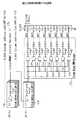
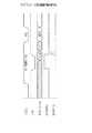
図1は、メモリデバイス(SDRAM)10の概略を説明するためのブロック図である。
メモリデバイス10は、CPU(図示略)に接続され、該CPUは、アクセス開始前の1回又は随時アクセス形態情報をメモリデバイス10に与える。メモリデバイス10は、アクセス形態情報に従って論理アドレスマップ形状を変更する機能を持つ。詳述すると、メモリデバイス10は、外部(CPU)より印加されるアクセス形態情報に応答して論理アドレスマップ形状を変更する。従って、CPUは、メモリデバイス10の論理アドレスマップ形状を制御するメモリコントローラとして機能する。
【0032】
論理アドレスマップ形状は、XアドレスとYアドレスの深さにより決定される。メモリセルアレイの容量は一定である。従って、メモリデバイス10は、Xアドレスの深さとYアドレスの深さを相補的に変更する。
【0033】
メモリデバイス10は、複数の論理アドレスマップ形状により、Xアドレスの最大値とYアドレスの最大値をそれぞれ指定するために必要なビット数のアドレス信号を外部アドレス端子から入力する。そして、このメモリデバイス10は、実質的に同じメモリ容量を持つ規格化されたメモリデバイスと同じ外形形状を有している。
【0034】
例えば、64Mビットの容量を持つメモリデバイス(32I/O,4バンク構成)は、一般的(標準規格)に、各バンクに1I/Oについて0.5MBのメモリセルを持つ。各バンクは2ビットのバンクアドレスにより選択される。各バンクのメモリセルは、11ビットのロウアドレス(Xアドレス)により選択される複数(2048本)のワード線と、8ビットのコラムアドレス(Yアドレス)により選択される複数(256本)のビット線によりアレイ配列されている。そして、SDRAM等のメモリデバイスは、アドレスマルチプレクス方式によりXアドレスとYアドレスを取り込むように構成されている。従って、一般的なメモリデバイスは、13本のアドレスピンを備え、それらから13ビットのXアドレス(うち2ビットのバンクアドレス)と、Yアドレスを時分割で取り込む。
【0035】
次に、メモリデバイス10の機能構成を説明する。
メモリデバイス10は、クロックバッファ11、コマンドデコーダ12、アドレスバッファ13、入出力バッファ14、制御信号ラッチ15、モードレジスタ16、アドレス発生回路17、書き込み・読み出し(I/O)制御回路18及びDRAMコア19を有する。
【0036】
クロックバッファ11は、クロックイネーブル信号CKE及び外部クロック信号CLKを外部装置から入力し、それらに基づいて生成した内部クロック信号CLK1を各回路へ出力する。
【0037】
コマンドデコーダ12は、クロックバッファ11からの内部クロック信号CLK1、つまりクロック信号CLKに応答して、外部装置から外部コマンドCOMを入力する。外部コマンドCOMは、本実施形態では、チップセレクト信号/CS、コラムアドレスストローブ信号/CAS、ライトイネーブル信号/WE及びロウアドレスストローブ信号/RASから構成されている。そして、コマンドデコーダ12は、内部クロック信号CLK1に応答して、その時に外部コマンドCOM、即ち、各信号/CAS,/WE,/CS,/RASの状態(Hレベル又はLレベル)からライトコマンド、リードコマンド、リフレッシュコマンド等の各種のコマンドをデコードする。そして、コマンドデコーダ12は外部コマンドCOMからこれらデコードした各種コマンドを内部コマンド及びイネーブル信号等としてアドレスバッファ13、入出力バッファ14、制御信号ラッチ15、モードレジスタ16及びI/O制御回路18に出力する。
【0038】
アドレスバッファ13は、バッファ機能及びラッチ機能を有し、コマンドデコーダ12からの内部コマンドに基づいて外部装置からアドレス信号A0〜A10とバンクアドレス信号BA0,BA1を入力する。アドレスバッファ13は、入力したアドレス信号A0〜A10及びバンクアドレス信号BA0,BA1を増幅し、それらに基づくアドレスデータをラッチするとともに制御信号ラッチ15、モードレジスタ16及びアドレス発生回路17に出力する。
【0039】
入出力バッファ14は、コマンドデコーダ12からのイネーブル信号に基づいて活性化され、外部装置からライトデータDQ0〜DQ31、マスク制御信号DQMを入力する。入出力バッファ14は、内部クロック信号CLK1に応答してライトデータDQ0〜DQ31をI/O制御回路18に出力する。また、入出力バッファ14は、内部クロック信号CLK1に応答してI/O制御回路18からのリードデータDQ0〜DQ31を外部装置に出力する。また、入出力バッファ14は、マスク制御信号DQMに応答してライトデータDQ0〜DQ31をマスクする。
【0040】
制御信号ラッチ15は、コマンドデコーダ12からの内部コマンド及びアドレスバッファ13からのアドレスデータを入力する。そして、制御信号ラッチ15は、これら内部コマンド及びアドレスデータに基づいてDRAMコア19に対してライトデータの書き込み、リードデータの読み出し、リフレッシュ、セルフリフレッシュ等の各種の処理動作のための制御信号を出力する。
【0041】
モードレジスタ16は、コマンドデコーダ12からの内部コマンド(モードレジスタセットコマンド)及びアドレスバッファ13からのアドレスデータを入力する。そして、モードレジスタ16は、これら内部コマンド及びアドレスデータに基づいてDRAMコア19に対して行う各種の処理動作のモードを保持する。そして、モードレジスタ16は、保持したモードの情報に基づく制御信号を出力する。
【0042】
モードレジスタ16が保持するモードの情報には、アクセス形態情報が含まれる。アクセス形態情報は、DRAMコア19の論理アドレスマップ形状を示す情報である。モードレジスタ16は、そのアクセス形態情報に基づいて生成したアドレス構成選択信号をアドレス発生回路17に出力する。
【0043】
アドレス発生回路17は、アドレスバッファ13からアドレス信号A0〜A10に基づくアドレスデータを入力する。そして、アドレス発生回路17は、モードレジスタ16のモードとアドレス構成選択信号に基づいて、その時々のDRAMコア19の論理アドレスマップ形状に対応して生成したロウアドレスデータとコラムアドレスデータをDRAMコア19に出力する。アドレス発生回路17は、モードレジスタ16に設定されたバースト長に基づいて入力アドレスからインクリメントしたコラムアドレスを自動生成する機能を有する。
【0044】
I/O制御回路18は、コマンドデコーダ12からの内部コマンドに基づいて、入力又は出力制御する。I/O制御回路18は、入出力バッファ14からのライトデータ(32ビット)をDRAMコア19に出力し、DRAMコア19からのリードデータ(32ビット)を入出力バッファ14に出力する。
【0045】
DRAMコア19は、複数(本実施形態では4つ)のバンクから構成され、各バンクには、制御信号ラッチ15からの制御信号、アドレス発生回路17からのロウアドレスデータとコラムアドレスデータをそれぞれ入力する。即ち、アドレスバッファ13にはDRAMコアのバンクの数に対応するバンクアドレス信号BA0,BA1が入力され、制御信号ラッチ15及びアドレス発生回路17は、各バンク毎に設けられている。
【0046】
DRAMコア19は、制御信号及びアドレスデータに基づいて内蔵したメモリセルアレイに対してライトデータの書き込み、リードデータの読み出し、リフレッシュ、セルフリフレッシュ等の各種の処理動作を実行する。従って、DRAMコア19は、入出力バッファ14から入力されたライトデータDQ0〜DQ31を制御信号及びアドレスデータに基づいて所定のアドレスのメモリセルに書き込む。
【0047】
図2は、DRAMコア19の概略構成図である。尚、説明の簡素化のため、ここではDRAMコア19を構成する1つのバンクについて説明する。
DRAMコア19の各バンクはメモリセルアレイ21を含み、メモリセルアレイ21は、複数のメモリセルがアレイ配置されて構成されている。各メモリセルは、ワード線WLとビット線(図示略)に接続され、ビット線はセンスアンプS/Aに接続されている。センスアンプS/Aにはコラム選択線CLが接続されている。即ち、メモリセルアレイ21は、Xアドレス(ロウアドレス)によりワード線WLが展開されるX展開方向と、Yアドレス(コラムアドレス)によりコラム選択線CLとセンスアンプS/A(S/A列)が展開されるY展開方向とにアレイ展開されている。
【0048】
メモリセルアレイ21は、そのX展開方向に区画される複数のロウブロック(Row Block )と、Y展開方向に区画される複数のコラムブロック(Column Block)を有する。ここで、ロウブロックは、メモリセルアレイ21のX展開方向に於いて各センスアンプS/A(S/A列)で区画される領域である。また、コラムブロックは、メモリセルアレイ21のY展開方向に於いてワード線WLに接続されるサブワード線SWL単位で区画される領域である。
【0049】
メモリセルアレイ21は、モードレジスタ16が保持するアクセス形態情報に応じて論理アドレスマップ形状を変更する機能を有し、この論理アドレスマップ形状は、モードレジスタ16から出力されるアドレス構成選択信号(本実施形態では、以下、ページ(Page)長指定信号という)によって変更される。
【0050】
詳述すると、メモリセルアレイ21は、ページ長指定信号によりXアドレスとYアドレスとを可変して論理アドレスマップ形状を変更する。そして、ページ長指定信号によりページ長(Yアドレスの深さ)が変更されると、それに応じて活性化されるセンスアンプS/Aの数が変更される。つまり、連続アクセスできるデータ数が変更される。
【0051】
このように構成されるDRAMコア19は、予め定められた本数の外部アドレス端子から入力されたアドレス信号A0〜A10、バンクアドレス信号BA0〜BA1に基づく所定のXアドレス、Yアドレスのメモリセルに対してデータの書き込み、読み出し等の各種の処理動作を実行する。
【0052】
尚、外部アドレス端子の本数は、Xアドレスの取り込み時に必要とする端子数またはYアドレスの取り込み時に必要とする端子数のいずれか多い方の端子数に設定されている。詳しくは、XアドレスがMビット、YアドレスがNビットに設定されたメモリデバイス10において、例えばM>Nの場合、外部アドレス端子の本数はM本に設定される。即ち、本実施形態のメモリデバイス(SDRAM)10では、最大で13ビットのXアドレス(ロウアドレス、バンクアドレスを含む)を取り込むための13本の外部アドレス端子が備えられている。
【0053】
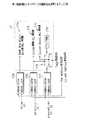
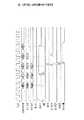
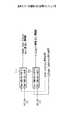
図3は、メモリデバイス10の制御方法を説明するブロック図である。
以下の説明では、外部アドレス端子の本数をM本とし、ページ長指定信号によりページ長が最大値(以下、フルページ)に設定される場合のXアドレスをMビット(XA<0:m>,(m=M−1))、YアドレスをNビット(YA<0:n>,(n=N−1))とする(ただし、M>N)。尚、同図では、説明の便宜上、アドレスバッファ13(図1参照)は第1〜第3アドレスバッファ13a〜13cに機能的に分割した状態で示すが、分割しない状態で構成してもよい。
【0054】
今、モードレジスタ16からのページ長指定信号に基づいてフルページより短いページ長が設定され、そのページ長指定信号により増加するXアドレスがiビットとする。このとき、Yアドレスは、iビット減少する。これは、メモリセルアレイ21の実質的な容量(2M+N)×I/O数が変化しないからである。そして、その増加したiビットのXアドレスは、Yアドレスの取り込み時に不要となる(M−N+i)本の外部アドレス端子のうちのi本から取り込まれる。
【0055】
詳述すると、第1アドレスバッファ13aは、コマンドデコーダ12からの内部コマンド(図中、Row Address 取り込み信号)に基づいてアドレス信号A0〜Amを入力する。第1アドレスバッファ13aは、入力したアドレス信号A0〜Amを増幅し、それらに基づくXアドレスデータをラッチするとともにアドレス発生回路17に出力する。
【0056】
第2アドレスバッファ13bは、コマンドデコーダ12からの内部コマンド(図中、Column Address取り込み信号)に基づいてアドレス信号A0〜A(n−i)を入力する。第2アドレスバッファ13bは、入力したアドレス信号A0〜A(n−i)を増幅し、それらに基づくYアドレスデータをラッチするとともにアドレス発生回路17に出力する。
【0057】
第3アドレスバッファ13cは、コマンドデコーダ12からの内部コマンド(図中、Column Address取り込み信号)に基づいてアドレス信号A(n−i+1)〜Anを入力する。第3アドレスバッファ13bは、入力したアドレス信号A(n−i+1)〜Anを増幅し、それらに基づくXアドレスデータ又はYアドレスデータをラッチするとともにアドレス発生回路17に出力する。
【0058】
アドレス発生回路17は、第1〜第3デコーダ(図中、各選択回路)17a〜17c、クランプ回路17d、及びスイッチ回路17eを含む。
第1〜第3デコーダ17a〜17cは、第1〜第3アドレスバッファ13a〜13cからのアドレスデータに基づいて、バンク(BANK)、ロウブロック(Row Block )、ワード線WL、コラムブロック(Column Block)、コラム選択線CLを各デコーダの機能に応じて適宜選択する。クランプ回路17dは、入力した任意のアドレスデータを無効化し、デコードの圧縮率を可変させる。尚、説明の便宜上、本実施形態では、アドレス発生回路17は第1〜第3デコーダ17a〜17cに機能的に分割した状態で構成したが、分割しない状態で構成してもよい。
【0059】
以下、詳述すると、第1デコーダ17aは、第1アドレスバッファ13aから出力されるXアドレスデータに基づいてバンク、ロウブロック、及びワード線WLを選択し、それらに対応するXアドレスをDRAMコア19に出力する。
【0060】
第2デコーダ17bは、第2アドレスバッファ13bから出力されるYアドレスデータに基づいてコラム選択線CLを選択し、それに対応するYアドレスをDRAMコア19に出力する。
【0061】
ここで、ページ長指定信号によってフルページよりも短いページ長が指定される場合、そのページ長指定信号によりスイッチ回路17eが所定の接続位置に切り替えられ、第3アドレスバッファ13cが第3デコーダ17cと接続される。
【0062】
これにより、第3デコーダ17cは、第3アドレスバッファ13cから出力されるXアドレスデータに基づいてコラムブロック(具体的にはワード線WL)を選択し、それに対応するXアドレスをDRAMコア19に出力する。つまり、ページ長指定信号により増加したiビットのXアドレスは、Yアドレスの取り込み時に不要となる(M−N+i)本の外部アドレス端子のうちのi本から取り込まれる。また、このときスイッチ回路17eによって第2デコーダ17bがクランプ回路17dに接続される。これにより、クランプ回路17dは、Yアドレスの取り込み時において、不要となるYアドレスを無効化する。
【0063】
尚、ページ長指定信号によってフルページが指定される場合には、第3アドレスバッファ13cが第2デコーダ17bと接続される。これにより、第2デコーダ17bは、第3アドレスバッファ13cから出力されるYアドレスデータに基づいてコラム選択線CLを選択し、それに対応するYアドレスをDRAMコア19に出力する。また、このとき、クランプ回路17dは、第3デコーダ17cに接続され、Yアドレスの取り込み時において、不要となるXアドレスを無効化する。
【0064】
尚、比較のため、従来のメモリデバイスの制御方法を説明するブロック図を図33に示す。従来では、Xアドレスを取り込むためのアドレスバッファ51と、Yアドレスを取り込むためのアドレスバッファ52がそれぞれ設けられる。そして、ページ長を短く使用する際には、そのときに増加したXアドレス又はYアドレスのビット数に応じて外部アドレス端子の本数(M又はN)を増加させるようにする。
【0065】
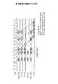
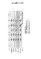
図7は、本実施形態のメモリデバイス10の内部動作を示す波形図である。尚、ここでは、例として64Mbit(メガビット)SDRAM(32I/O)の動作波形図を示す。
【0066】
今、初期状態において、メモリデバイス10は、13ビットのXアドレス(ロウアドレスRA<0:10>、バンクアドレスBA<0:1> )、8ビットのYアドレス(コラムアドレスCA<0:7> )よりなる論理アドレスマップ形状を有し、ページ長が256(フルページ)に設定されている。
【0067】
メモリデバイス10は、モードレジスタセットコマンドMRSに応答して、アドレス信号A0〜A10をアドレスコードCode(CodeA<0:10>) として取り込むとともに、バンクアドレスBank(BA<0:1>) を取り込む。そして、メモリデバイス10は、アドレスコードCode(CodeA<0:10>) に基づいて、ページ長Page、キャスレイテンシtCL、バースト長BL等の各種設定を行う。
【0068】
今、キャスレイテンシtCL=3、バースト長BL=2、ページ長Page=32に設定される。このとき、メモリデバイス10は、16ビットのXアドレス(ロウアドレスRA<0:13>、バンクアドレスBA<0:1> )、5ビットのYアドレス(コラムアドレスCA<0:4> )よりなる論理アドレスマップ形状に変更する。即ち、ページ長可変に伴い、ロウアドレスが3ビット分増加する。
【0069】
メモリデバイス10は、アクティブコマンドACTに応答してアドレス信号A0〜A10をロウアドレスRow(RA<0:10>)として取り込むとともにバンクアドレスBank(BA<0:1>) を取り込む。尚、バンクアドレスの取り込みは、以降同じであるため省略する。
【0070】
尚、モードレジスタセットコマンドMRS入力時に設定したページ長(=32)は、このアクティブコマンドACT入力時に設定するようにしてもよい。この場合、ページ長を設定するために必要なビット数分取り込むロウアドレスが少なくなる。例えば、ページ長の設定に2ビット必要な場合、メモリデバイス10は、アドレス信号A0〜A8をロウアドレスRow(RA<0:8> )として取り込み、アドレス信号A9,A10を設定情報として取り込む。又は、アクティブコマンドACT入力時に使用しない他ピン(DQマスクピンなど)から取り込んでもよい。
【0071】
次いで、メモリデバイス10は、アクティブコマンドACT入力後の所定クロック後(例えば2クロック後)に入力されるリードコマンドRD1に応答して、アドレス信号A0〜A5をコラムアドレスCol(CA<0:4>) として、アドレス信号A6〜A8をロウアドレスRow(RA<11:13>) として取り込む。
【0072】
つまり、ページ長可変に伴い増加する3ビットのロウアドレスRowは、リードコマンドRD1の入力時において、コラムアドレスCol(CA<0:4>) の取り込み時に不要となる外部アドレス端子から取り込まれる。そして、メモリデバイス10は、そのロウアドレスRow(RA<11:13>) に基づいてコラムブロック、ワード線WLを選択し、その選択したワード線WL及びそれに対応するセンスアンプS/Aを活性化させる。
【0073】
尚、アクティブコマンドACTに応答してアドレス信号A0〜A10をロウアドレスRow(RA<3:13>)として取り込み、リードコマンドRD1に応答してアドレス信号A6〜A8をロウアドレスRow(RA<0:2> )として取り込む構成としてもよい。また、リードコマンドRD1に応答してアドレス信号A6〜A8をロウアドレスRowの任意のビット位置に取り込む構成としても良い。
【0074】
メモリデバイス10は、リードコマンドRD1が発行されると、設定されたキャスレイテンシtCL(=3)及びバースト長BL(=2)に基づいて、該リードコマンドRD1入力後の3クロック後にリードデータD11,D12を順次出力する。
【0075】
その後、メモリデバイス10は、リードコマンドRD2,RD3に順次応答して、コラムアドレスCol(CA<0:4>) 及びバンクアドレスBank(BA<0:1>) を取り込む。この際、2回目以降のリードコマンドRD2,RD3では、増加したロウアドレスRowは取り込まれず、コラムアドレスCol(CA<0:4>) 及びバンクアドレスBank(BA<0:1>) のみ取り込まれる。
【0076】
尚、本実施形態では、リードコマンドRD1〜RD3について説明したが、ライトコマンドの場合についても同様である。即ち、アクティブコマンドACT入力後の最初のライトコマンドにて、増加したロウアドレスRow(RA<11:13>) が取り込まれる。そして、2回目以降のライトコマンドでは、コラムアドレスCol(CA<0:4>) 及びバンクアドレスBank(BA<0:1>) のみが取り込まれる。
【0077】
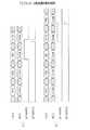
尚、比較のため、従来のメモリデバイスの内部動作を示す波形図を図34及び図35に示す。
図34は、ページ長Pageが256(フルページ)に設定される場合の64Mbit(メガビット)SDRAMの動作波形図である。同図に示すように、モードレジスタセットコマンドMRS入力後において、メモリデバイスは、アクティブコマンドACTに応答して、ロウアドレスRow(RA<0:10>)を取り込む。次いで、メモリデバイスは、リードコマンドRD1〜RD3に順次応答して、コラムアドレスCol(CA<0:7> )を取り込む。
【0078】
図35は、ページ長Pageが32に設定された64Mbit(メガビット)SDRAMの動作波形図である。同図に示すように、短いページ長(=32)を使用する場合には、ロウアドレスRowが3ビット増加する。即ち、メモリデバイスは、アクティブコマンドACTに応答してアドレス信号A0〜A10をロウアドレスRow(RA<0:10>)として取り込み、アドレス信号A13〜A15を増加したロウアドレスRow(RA<11:13>) として取り込む。従って、従来では、短いページ長(=32)に設定されたメモリデバイスは、増加した3ビットのロウアドレスRowを取り込むための外部アドレス端子数が規格品に比べて増加する。
【0079】
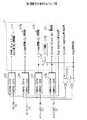
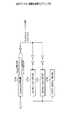
図8は、図7におけるアクティブコマンドACT発行後のアクセス制御を説明するブロック図である。尚、同図において、図3と同様の構成部分には、同一符号を付してその詳細な説明を一部省略する。
【0080】
コマンドデコーダ12(図1参照)は、コマンド判定回路(図中、Command 判定回路)12aと、コマンド判定回路12aから出力される最初の活性化信号を検出するページコマンド1回目検出回路(図中、Page Command1回目検出回路)(以下、コマンド検出回路)12bを含む。尚、本実施形態において、活性化信号は、ワード線WL及びセンスアンプS/Aを活性化させる信号である。
【0081】
コマンド判定回路12aは、内部クロック信号CLK1に応答してデコードした各種コマンドのうち、リードコマンドとライトコマンドを判定し、判定に応じてリード活性化信号又はライト活性化信号を出力する。
【0082】
今、図7に示すリードコマンドRD1入力時においては、コマンド判定回路12aは、リード活性化信号を出力する。
第2アドレスバッファ13b(図中、Address Latch )は、オア回路31及び遅延回路32を介して入力されるリード活性化信号(リードコマンドRD1)に基づいてアドレス信号A0〜A4を入力する。そして、第2アドレスバッファ13bは、それらアドレス信号A0〜A4に基づくコラムアドレスデータを第2デコーダ17b(図中、Column Address Decoder)に出力する。
【0083】
第3アドレスバッファ13c(図中、Address Latch )は、オア回路31を介してコマンド検出回路12bに入力される1回目のリード活性化信号(リードコマンドRD1)により、当該コマンド検出回路12bから出力される検出信号に基づいてアドレス信号A5〜A7を入力する。そして、第3アドレスバッファ13cは、それらアドレス信号A5〜A7に基づくロウアドレスデータを第3デコーダ17c(図中、Column Block 選択用 Address Decoder)に出力する。
【0084】
第2デコーダ17bは、第2アドレスバッファ13bから出力されるコラムアドレスデータに基づいてコラム選択線CLを選択する。
第3デコーダ17cは、第3アドレスバッファ13cから出力されるロウアドレスデータに基づいてコラムブロック、ワード線WLを選択する。これにより、ワード線WL及びセンスアンプS/Aが活性化される。
【0085】
このようにして、コマンド検出回路12bは、コマンド判定回路12aから出力される1回目のリード活性化信号(リードコマンドRD1)のみを検出し、そのコマンド検出回路12bからの検出信号に基づいて、拡張されたロウアドレスRow(RA<11:13>) が第3デコーダ17cに保持される。
【0086】
そして、2回目のリード活性化信号(図7に示すリードコマンドRD2)ではコマンド検出回路12bから検出信号が出力されない。つまり、2回目以降に発行されるリードコマンドRD2,RD3では、アドレス信号A5〜A7は第3アドレスバッファ13cに取り込まれない。
【0087】
尚、図13及び図14は、上述した図8の具体的な回路構成の一例を示す回路図である。又、図15は、図13及び図14に示す回路の内部動作の一例を示す波形図である。
【0088】
尚、比較のため、従来のアクセス制御を説明するブロック図を図36に示す。同図は、従来のアクセス制御の原理を説明するものであるので、同様の機能を持つ構成部分については、同一符号を付す。図36に示すように、従来では、ページ長が256であるため、コラムアドレスCol(CA<0:4>) とともにコラムアドレスCol(CA<5:7>) がリード又はライト活性化信号(即ち、リード又はライトコマンド)の出力毎に取り込まれる。
【0089】
図9は、図8にて説明したアクセス制御をページ長に応じて行う場合について説明するブロック図である。
この構成では、ページ長指定信号に基づいて各スイッチ回路33a,33bの接続位置を切替えることで、第2及び第3アドレスバッファ13b,13cにてラッチするアドレス信号をページ長に応じて適宜変更することができる。これにより、第2及び第3デコーダ17b,17cは、ページ長に応じたその時々のDRAMコア19の論理アドレスマップ形状に対応して生成したロウアドレスとコラムアドレスをDRAMコア19に出力する。
【0090】
図10は、ワード線WL及びセンスアンプS/Aの活性化制御を説明する概略ブロック図である。
同図に示すように、ワード線活性化回路41及びセンスアンプ活性化回路42は、ページ長指定信号に応じて入力されるコマンド判定回路12a又はコマンド検出回路12bのいずれかの出力信号に応答してワード線WL、センスアンプS/Aをそれぞれ活性化させる。
【0091】
詳しくは、ページ長指定信号によりページ長Pageがフルページに設定される場合、各活性化回路41,42は、コマンド判定回路12aからのアクティブ信号(アクティブコマンド)に応答してワード線WL、センスアンプS/Aをそれぞれ活性化させる。これは、アクティブコマンドの受け付け時にワード線WL及びセンスアンプS/Aを選択するために必要なロウアドレスの全てのビットがそろうからである。
【0092】
一方、ページ長指定信号によりページ長Pageがフルページよりも短いページ長に設定される場合、各活性化回路41,42は、検出回路12aからの検出信号、つまりリード又はライト活性化信号(リード又はライトコマンド)に応答してワード線WL、センスアンプS/Aをそれぞれ活性化させる。これは、活性化するワード線WL及びセンスアンプS/Aを選択するために、アクティブコマンドにより受け付けるロウアドレスと、ページコマンドにより受け付けるロウアドレスとが必要となるからである。
【0093】
尚、比較のため、従来の活性化回路の制御方法を説明するブロック図を図37に示す。同図は、従来の活性化制御の原理を説明するものであるので、同様の機能を持つ構成部分については、同一符号を付す。図37に示すように、従来では、各活性化回路41,42は、コマンド判定回路12aからのアクティブ信号によってのみ、ワード線WL、センスアンプS/Aをそれぞれ活性化させる。
【0094】
以上記述したように、本実施形態によれば、以下の効果を奏する。
(1)メモリデバイス10は、モードレジスタ16から出力されるページ長指定信号に応じて、DRAMコア19の論理アドレスマップ形状を変更する。そして、ページ長がフルページより短く設定される場合には、それにより増加したロウアドレスRowが、最初のリードコマンドRD1入力時に取り込まれる。このように、増加するロウアドレスRowが、その時に使用されていない外部アドレス端子を使用して時分割で取り込まれるため、外部アドレス端子の本数や配列を変更することなくページ長を変更でき、汎用パッケージを使用することができる。従って、開発期間の長期化やコスト増加を抑止することができる。
【0095】
(2)パッケージを変更することなくページ長を変更することができるため、メモリデバイスを使用する顧客のシステムに応じた効率的なアクセス方法が実現可能となる。
【0096】
(3)また、パッケージを変更することなく、ページ長を短く使用することができるため、センスアンプS/Aの活性化数を必要最小限まで少なくすることができ、消費電流の低減化を図ることができる。
【0097】
(第二実施形態)
以下、本発明を具体化した第二実施形態を説明する。
本実施形態は、第一実施形態のメモリデバイス10を使用して、同様にページ長を256から32に変更する場合に、そのページ長変更に伴い増加するロウアドレスの取り込み方法の他の制御方法を説明するものである。従って、同様な構成部分については、同一名称及び同一符号を付してその詳細な説明を一部省略する。
【0098】
図18は、第二実施形態の内部動作を示す波形図である。
本実施形態では、図18に示すように、リードコマンドRD1が、アクティブコマンドACTの1クロック後に入力される。つまり、アクティブコマンドACTが入力されてから最初のリードコマンドRD1が入力されるまでの時間tRCDがtRCD=1に設定され、当該リードコマンドRD1が第一実施形態よりも1クロック早く入力される。(ちなみに、第一実施形態では、tRCD=2(図7参照)。)
従って、ページ長変更(256から32に変更)に伴い増加するロウアドレスRow(RA<11:13> )が第一実施形態よりも1クロック分早く取り込まれ、それによりワード線WL及びそれに対応するセンスアンプS/Aがほぼ1クロック分早く活性化される。
【0099】
ところで、一般には、ワード線WLの活性化動作を完全に終了させるために、アクティブコマンドACT入力からリードコマンドRD1入力によってアクセス動作が開始されるまでの猶予(待ち)が必要である。この猶予期間は、クロック信号の周波数により異なるが現在使用されている機器の一般的なクロック周波数では通常2クロック必要である。従って、リードコマンドRD1に基づくアクセス動作の開始タイミングを、該リードコマンドRD1入力時から実質的に1クロック分遅らせる必要がある。
【0100】
一方、キャスレイテンシtCLは、リードコマンドの入力からリードデータの出力までの期間(クロック数)を規定するものである。このため、図18に示すように、最初のリードコマンドRD1に対応するキャスレイテンシtCLは、予め設定されたキャスレイテンシtCLの値、tCL=3(設定値)からtCL=4に変更される。従って、メモリデバイスは、リードコマンドRD1発行後の4クロック後にリードデータD11,D12を順次出力する。
【0101】
その後、メモリデバイスはリードコマンドRD2,RD3に応答してコラムアドレスCol(CA<0:4>) とバンクアドレスBank(BA<0:1>) を順次取り込み、予め設定されたキャスレイテンシtCL(tCL=3:設定値)に従ってリードデータを順次出力する。
【0102】
この際、前記と同様に、2回目以降のリードコマンドRD2,RD3では、増加したロウアドレスRowは取り込まれず、コラムアドレスCol(CA<0:4>) とバンクアドレスBank(BA<0:1>) のみ取り込まれる。尚、本実施形態では、リードコマンドRD1〜RD3について説明したが、ライトコマンドの場合についても同様である。
【0103】
図19は、キャスレイテンシtCLの制御方法を説明するブロック図である。本実施形態において、上記コマンドデコーダ12(図1参照)は、前記コマンド判定回路12a、ページコマンド1回目検出回路12b、及びキャスレイテンシ(Cas Latency )制御回路12cを含む。
【0104】
前記と同様に、コマンド判定回路12aは、リードコマンド又はライトコマンドであるか否か判定し、リード活性化信号又はライト活性化信号を出力する。コマンド検出回路12bは、コマンド判定回路12aから出力される最初のリード活性化信号又はライト活性化信号を検出し、その検出信号をキャスレイテンシ制御回路12cに出力する。
【0105】
キャスレイテンシ制御回路12cは、内部クロック信号CLK1に応答して予め定められた所定のクロック数で出力制御信号を出力し、内部コマンド(図18ではリードコマンドRD1〜RD3)が発行されてからその出力データが確定されるまでの時間つまりキャスレイテンシtCLを制御する。
【0106】
そして、キャスレイテンシ制御回路12cは、コマンド検出回路12bから検出信号が出力されると、その検出信号に応答してその時のキャスレイテンシtCLの値を変更する。尚、具体的には、本実施形態のキャスレイテンシ制御回路12cは、コマンド検出回路12bからの検出信号に応答して、キャスレイテンシtCLの値を予め定められた値(設定値)より1大きくする。
【0107】
つまり、図18において、キャスレイテンシtCLは、モードレジスタセットコマンドMRSによりtCL=3(設定値)に設定されている。次に、アクティブコマンドACT発行後、最初のリードコマンドRD1が入力されると、キャスレイテンシ制御回路12cには、コマンド検出回路12bから出力される検出信号が入力される。この検出信号に応答してキャスレイテンシ制御回路12cは、キャスレイテンシtCLの値(tCL=3:設定値)をtCL=4に変更する。即ち、キャスレイテンシ制御回路12cは、最初のリードコマンドRD1入力時のみtCL=4に変更し、2回目以降のリードコマンドRD2,RD3ではtCL=3にする。
【0108】
以上記述したように、本実施形態によれば、以下の効果を奏する。
(1)本実施形態では、アクティブコマンドACT入力後の最初のリードコマンドRD1が第一実施形態よりも1クロック分早く入力されることで、ページ長可変に伴い増加するロウアドレスRowが第一実施形態よりも1クロック分早く取り込まれる。従って、ワード線WL及びセンスアンプS/Aをほぼ1クロック分早く活性化させることができる。その際、キャスレイテンシ制御回路12cによってリードコマンドRD1に対応するキャスレイテンシtCLがtCL=4に変更されることで、ワード線WLとセンスアンプS/Aを活性化させてからリードデータを出力するまでの期間が十分に確保される。これにより、ページ長可変時において、リードコマンドRD1に基づくアクセス動作の開始タイミングが遅れることはない。
【0109】
(第三実施形態)
以下、本発明を具体化した第三実施形態を説明する。
本実施形態は、第一実施形態のメモリデバイス10を使用して、同様にページ長を256から32に変更する場合に、そのページ長変更に伴い増加するロウアドレスの取り込み方法の他の制御方法を説明するものである。従って、同様な構成部分については、同一名称及び同一符号を付してその詳細な説明を一部省略する。
【0110】
図20は、第三実施形態のアクセス制御を説明するブロック図である。
本実施形態において、上記コマンドデコーダ12(図1参照)は、前記コマンド判定回路12a及び所定時間検出回路(以下、時間検出回路)12dを含む。
【0111】
検出回路12dには、内部クロック信号CLK1と、コマンド判定回路12aから出力されるアクティブ(Active)信号及びリード又はライト活性化信号が入力される。
【0112】
つまり、コマンド判定回路12aは、内部コマンドがアクティブコマンドACTである場合にアクティブ信号を出力する。時間検出回路12dは、アクティブ信号に応答し、予め定めた所定時間(以下、アドレスレイテンシtALという)経過後に、増加したロウアドレスを取り込むためのアドレス取込信号を出力する。
【0113】
尚、本実施形態において、アドレスレイテンシtALは、内部クロック信号CLK1に基づいて設定され、時間検出回路12dは内部クロック信号CLK1に基づく所定クロック数をカウントした後、アドレス取込信号を出力する。そして、このとき時間検出回路12dは、コマンド判定回路12aから最初のリード活性化信号又はライト活性化信号が出力されるまで、アドレス取込信号を出力する。
【0114】
今、ページ長が32に設定されるとき、そのページ長指定信号によりスイッチ回路33が図20に示す接続位置に切替えられる。
第3アドレスバッファ13cは、時間検出回路12dからのアドレス取込信号に基づいて入力したアドレス信号A0〜Anを増幅し、それらに基づくロウアドレスデータをラッチして第3デコーダ17cに出力する。そして、第3デコーダ17cは、ロウアドレスデータに対応するコラムブロック(ワード線WL)を指定するためのロウアドレス(RA<0:n> )をDRAMコア19(図1)に出力する。
【0115】
ちなみに、図20に示すように、時間検出回路12dからの検出信号に基づいて取り込まれるロウアドレス(増加したロウアドレス)は、ページ長指定信号に基づいて第2及び第3バッファ13b,13cのいずれかにて取り込まれる。尚、図22は、図20の時間検出回路12dの具体的な回路構成の一例を示す回路図である。
【0116】
図21は、本実施形態の内部動作を示す波形図である。尚、同図では、時間検出回路12dのアドレスレイテンシtALが、例えばtAL=1に設定される場合について説明する。
【0117】
図21に示すように、ページ長可変(256から32に変更)に伴い増加したロウアドレスRow(RA<0:4>) は、アクティブコマンドACT入力後の1クロック後に、時間検出回路12dからのアドレス取込信号によって取り込まれる。これにより、コラムブロック及びワード線WLが選択され、選択されたワード線WL及び対応するセンスアンプS/Aが活性化される。
【0118】
その後、メモリデバイス10は、リードコマンドRD1〜RD3に順次応答してコラムアドレスCol(CA<0:4> )及びバンクアドレスBank(BA<0:1>) を取り込み、予め設定されたキャスレイテンシ(tCL=3)、バースト長(BL=2)に従ってリードデータを順次出力する。この際、前記同様に、各リードコマンドRD1〜RD3において、増加したロウアドレスRowは取り込まれず、コラムアドレスCol(CA<0:4>) 及びバンクアドレスBank(BA<0:1>) のみ取り込まれる。尚、本実施形態では、リードコマンドRD1〜RD3について説明したが、ライトコマンドの場合についても同様である。
【0119】
以上記述したように、本実施形態によれば、以下の効果を奏する。
(1)コマンドデコーダ12は、コマンド判定回路12aからのアクティブ信号に応答して所定時間(アドレスレイテンシtAL)経過後にアドレス取込信号を出力する時間検出回路12dを備える。これにより、ページ長可変に伴い増加したロウアドレスRowは、アクティブコマンドACTの1クロック後(tAL=1)に取り込まれる。従って、第二実施形態と同様、ワード線WL及びセンスアンプS/Aをはやく活性化させることができる。また、本実施形態では、増加したロウアドレスRowがリードコマンドRD1入力よりも早いタイミングで取り込まれるため、その取り込み時において、外部アドレス端子の配列に左右されない。
【0120】
(2)アクティブコマンドACTとリードコマンドRDのタイミング、及びそれらの出力時に指定するアドレス信号はページ長(論理アドレスマップ形状)によらない。すなわち、メモリコントローラ(CPU)アクティブコマンドACTとリードコマンドRDの間に拡張されるロウアドレスに対応するアドレス信号を出力するだけである。従って、変更が容易であり、手間をかけることなく新たな機能(論理アドレスマップ形状を変更する機能)を利用することができる。
【0121】
(第四実施形態)
以下、本発明を具体化した第四実施形態を説明する。
本実施形態は、第三実施形態における時間検出回路12dのアドレスレイテンシtALが、例えばtAL=0.5に設定される場合について説明するものである。
【0122】
図23は、第四実施形態の内部動作を示す波形図である。
本実施形態では、図23に示すように、ページ長変更(256から32に変更)に伴い増加するロウアドレスRowは、アクティブコマンド入力後の0.5クロック後に、時間検出回路12dからのアドレス取込信号によって取り込まれる。
【0123】
つまり、メモリデバイス10は、アクティブコマンドACTの入力に基づくクロック信号CLKの立上がりエッジでロウアドレスRow(RA<0:10>)を取り込み、その0.5クロック後におけるクロック信号CLKの立下がりエッジで増加したロウアドレスRow(RA<0:4>) を取り込む。
【0124】
このように、本実施形態では、アドレスレイテンシtAL=0.5に設定することにより、増加したロウアドレスRowが第三実施形態よりも0.5クロック分早く取り込まれ、それによりワード線WL及び対応するセンスアンプS/Aがほぼ0.5クロック分はやく活性化される。
【0125】
その後、メモリデバイス10は、リードコマンドRD1〜RD3に順次応答してコラムアドレスCol(CA<0:4> )及びバンクアドレスBank(BA<0:1>) を取り込み、予め設定されたキャスレイテンシ(tCL=3)、バースト長(BL=2)に基づいてリードデータを順次出力する。この際、前記同様に、各リードコマンドRD1〜RD3において、増加したロウアドレスRowは取り込まれず、コラムアドレスCol(CA<0:4>) 及びバンクアドレスBank(BA<0:1>) のみ取り込まれる。尚、本実施形態では、リードコマンドRD1〜RD3について説明したが、ライトコマンドの場合についても同様である。
【0126】
以上記述したように、本実施形態によれば、以下の効果を奏する。
(1)本実施形態では、アドレスレイテンシtALが、tAL=0.5に設定されるため、ページ長可変に伴い増加したロウアドレスRowが、アクティブコマンドACTの0.5クロック後に取り込まれる。従って、ワード線WL及びセンスアンプS/Aを第三実施形態よりもほぼ0.5クロック分早く活性化させることができる。これにより、ページ長可変時において、リードコマンドRD1に基づくアクセス動作の開始タイミングが遅れることはない。
【0127】
尚、上記各実施形態は、以下の態様で実施してもよい。
・上記各実施形態において、メモリセルのビット数、アドレス構成、アドレス構成の切替え種類などは、この例に限定されない。
【0128】
・図3において、クランプ回路17dは、アドレス発生回路17内に設けたが、別途備えるようにしてもよい。
・図3の構成は、図4に示すように変更してもよい。即ち、アドレス信号A(n−i+1)〜Anに基づくYアドレス、Xアドレスを取り込むための専用のアドレスバッファ13f、13gをそれぞれ設けるようにしてもよい。
【0129】
・図3の構成は、図5に示すように変更してもよい。即ち、各アドレスバッファ13h〜13jが、それぞれXアドレス又はYアドレスを取り込むためのアドレスバッファを共有するように構成する。そして、それらの出力信号(Xアドレスデータ又はYアドレスデータ)をXY切替え信号によって適宜選択するようにしてもよい。
【0130】
・図3の構成は、図6に示すように変更してもよい。即ち、図5と同様に、各アドレスバッファ13k、13l、13nが、それぞれXアドレス又はYアドレスを取り込むためのアドレスバッファを共有するように構成し、ページ長可変に伴い増加するアドレス(Xアドレス)のみを取り込むためのアドレスバッファ13mを別途設けるようにしてもよい。
【0131】
・図8のコマンド判定回路12a、コマンド検出回路12bは、メモリデバイスが非同期型である場合には、クロック信号CLK1に依存しない他の構成に代えてもよい。
【0132】
・図10において、センスアンプ(S/A)活性化回路42のみ制御する構成としてもよい。
・図8の構成は、図11に示すように変更してもよい。即ち、第3アドレスバッファ13cは、コマンド判定回路12aからのリード/ライト活性化信号(即ちリード/ライトコマンド)毎にアドレス信号A5〜A7を毎回取り込む。そして、コマンド検出回路12bからの検出信号に基づいて、第3デコーダ17cが、2回目以降のリード/ライトコマンドでは、第3アドレスバッファ13cからのロウアドレスデータを再ラッチしないようにしてもよい。尚、図16及び図17は、図11の具体的な回路構成の一例を示す回路図である。
【0133】
・また、図12は、図11の構成によって行うアドレス制御をページ長に応じて行う場合について示す。この構成では、ページ長指定信号によりスイッチ回路33a,33bの接続位置が切替えられることにより、ページ長に応じたその時々のDRAMコア19の論理アドレスマップ形状に対応して生成したロウアドレス、コラムアドレスが第2及び第3デコーダ17b,17cからそれぞれ出力される。
【0134】
・第一及び第二実施形態では、ページ長可変に伴い増加したアドレスをアクティブコマンドACT入力後の最初のリード/ライトコマンドで取り込まれるYアドレスと同時に取り込むようにしたが、この例に限定されない。即ち、増加したアドレスを最初のリード/ライトコマンドにて取り込んだ後、当該コマンドの所定クロック後(例えば1クロック後)にYアドレスが取り込まれるようにしてもよい。
【0135】
・第三及び第四実施形態では、時間検出回路12dは、アクティブ信号に応答して所定クロック後に検出信号を出力するようにしたが、非同期型のメモリデバイスに具体化する場合には、内部クロック信号CLK1に依らず所定時間(tAL)経過後に検出信号を出力する構成としてもよい。
【0136】
・第四実施形態のように、アドレスレイテンシtAL=0.5にて増加したロウアドレスRowを取り込む方法を実現するその他の手段として、ダブルデータレート(Double Date Rate,DDR)方式を用いて具体化してもよい。即ち、クロック信号CLK、/CLK(/は、バー)で表現される2つのクロック信号を用いて、クロック信号CLKの立上りでロウアドレスを取り込み、直後の180度位相が異なるクロック信号/CLKの立上りで増加したロウアドレスを取り込むようにしてもよい。
【0137】
・上記各実施形態では、モードレジスタセットコマンドMRS入力時、又は1種類のアクティブコマンドACT入力時にページ長を指定するようにしたが、2種類のアクティブコマンドACTを用いて、それらアクティブコマンドACTの入力に基づいてページ長を指定するようにしてもよい。
【0138】
・上記各実施形態では、同期型のメモリデバイスに具体化したが、非同期型メモリにて論理アドレスマップ形状を変更可能に構成してもよい。尚、非同期型メモリの概略構成は既に公知であるため図面及び説明を省略する。
【0139】
このメモリデバイスは、チップイネーブル信号(/CE)もしくはロウアドレスストローブ信号(/RAS)の立ち下がりでアドレス信号ADDをXアドレス(ロウアドレス)として確定する。次に、メモリデバイスは、リードもしくはライト制御信号等でアドレス信号をYアドレス(コラムアドレス)として確定し、それらアドレスにて指定されるセルに対してアクセスを行なう。
【0140】
論理アドレスマップ形状の変更は、以下のイリーガルエントリー方式(通常外部からのアクセスでは使用しない外部からの制御方法)により行う。
イリーガルエントリー方式は、同期式でのモードレジスタセットコマンドを使用(MRS方式)した場合と同様に、メモリデバイス内部のアドレス構成セレクト信号をチップイネーブル信号/CEからのワード線活性化信号よりも早く生成する。これにより、アドレス発生回路もしくはその出力の切換え動作を遅らせることなくアクセス遅延を防止できる。
【0141】
イリーガルエントリー方式について詳述する。
図24はアドレス構成の為のモード設定サイクルを説明する波形図である。
メモリデバイスは、アドレス構成の為のモード設定用の専用端子を備え、その専用端子からアドレス構成の種類毎を決める為の情報に必要な情報を取り込むことで、外部アクセス遅延を防止でき誤動作を防止し通常動作の安全動作を保証できる。
【0142】
即ち、メモリデバイスはチップイネーブル信号/CE1がHレベルの時に通常動作を行わない。この期間に、専用端子から入力されるプログラムモード信号/PE(=アドレス構成設定端子)に応答してアドレス信号ADDに基づくアドレスコードCodeを取り込む。詳しくは、メモリデバイスは、プログラムモード信号/PEの立ち下がりでアドレスコードの入力を活性化し、同信号/PEの立ち上がりでアドレスコード情報をラッチする。
【0143】
一方、メモリデバイスは、チップイネーブル信号/CE1がLレベルの時、外部アクセスに対応した動作状態となり外部アクセスに対応したアドレス信号ADDを取り込む。
【0144】
尚、図中t1〜t5は外部仕様タイミング条件である。
尚、図のタイミングにおいて、プログラムモード信号/PEの立ち下がりで外部専用端子の入力回路を活性化し、アドレス信号に対するデコード動作を開始する。そして、プログラムモード信号/PEの立ち上がりでデコード結果を確定し、前記入力回路を非活性化する。この動作によって、消費電力の低減を図ることができる。
【0145】
上記したアドレス構成の為のモード設定サイクルにおいて、プログラムモード信号/PEの論理を反転してもよい。また、アドレスコードはデータ端子(DQやI/Oピンと呼んでいる)から入力しても良い。
【0146】
更に、後述の様に、前記コード方式によるプログラムサイクルを数回繰り返した後に、モードを確定するようにしても良い。
図25は、コマンドの説明図である。
【0147】
このコマンドを利用する場合は、基準クロック(システムクロックCLKやチップイネーブル信号/CE1)に対して、コマンド認識して外部アクセス動作を行なう仕様方式のメモリデバイスが対象となる。
【0148】
よって、チップイネーブル信号/CE1に対してコマンドで動作しない仕様方式のメモリデバイスでは、前記図7を基本に単にアドレスをアドレス構成の種類毎を決める為の情報として対応し、モード設定の為の回数として利用すればよい。
【0149】
コマンド(1)〜(6),(8)〜(10)は通常動作にて用いられるコマンドであり、コマンド(7),(11)は通常動作では意味をなさないコマンドである。コマンド(7)は、ライト(WR)動作であるが信号/LB,/UBがHレベルであるためデータを入力しない(マスクされている)。コマンド(11)は、リード(RD)動作であるが、同様に信号/LB,/IBによりマスクされているためデータを出力しない。
【0150】
このように、通常動作に用いないコマンド(イリーガルコマンド)をアドレス構成の種類毎を決める為の情報として取り込むことで、専用端子を設けることなく情報の設定を行うことができる。
【0151】
図26は、アドレス構成の為のモード設定サイクルを説明する波形図であり、図25のコマンド(11)を複数継続して入力することでアドレス構成の為のモード設定に必要な情報をアドレスコードとして取り込む場合を示す。
【0152】
メモリデバイスは、コマンド(11)に応答してアドレス信号ADDをアドレスコードCodeとして取り込む。この動作をN回繰り返す。1回目からN回目までコマンド(11)に対応して取り込んだN個のアドレスコードCodeが全て一致する場合に、そのアドレスコードCodeを有効にしてアドレス構成の為のモード設定を行う。
【0153】
尚、コマンド(11)がN?1回一致した場合に、N回目のコマンド(11)に対応して取り込んだアドレスコードCodeに基づいてアドレス構成の為のモード設定を行うようにしてもよい。また、アドレスコードCodeの取り込みを任意のサイクル(例えば1回目)に変更して実施しても良い。他にも種々の応用が展開できる。
【0154】
モードを設定するアドレスコードは、アドレス構成の種類数に対応してアドレスBit数を確定すればよい。
図26の様にN回のモード設定サイクルの場合、デバイス内部ではカウンタ回路を用いる。N回のモード設定サイクルのエントリに対してカウンタ回路の上位ビットが変化したら、モードを確定する回路構成となる。
【0155】
図27は、プログラムアドレス構成の為のモード設定回路であるエントリコントロール回路の動作波形図である。
図27(a)に示すように、第1エントリ回路は、3回目のサイクルでHレベルの第1のアドレスイネーブル信号proaddz を出力し、4回目のサイクルで第1のエントリ信号proentz を出力する。そして、第1エントリ回路は、第1のアドレスイネーブル信号proaddz 及び第1のエントリ信号proentz を同時にリセットする。これによりメモリデバイスは前に確定したアドレス構成の情報を、第1のエントリ信号proentz により4回目のサイクルで取り込んだアドレスコード情報に従った最新のアドレス構成の情報に変更される。
【0156】
図27(b)に示すように、第1エントリ回路は、カウントの途中でその他のコマンド(デバイス活性のアクティブコマンドやリード/ライトコマンド)を受け付けるとカウントをリセットする。その結果、第1のアドレスイネーブル信号proaddz 及びイネーブル信号proaddz をLレベルに保持する。
【0157】
つまりアドレス構成の種類毎を決める為のモード設定において、その為の同じコマンドが連続して規定回数続かなければキャンセルされる。(メモリデバイスは前に確定したアドレス構成の情報を維持する)
図28は、図24に対応したプログラムアドレス構成の為のモード設定回路であるエントリコントロール回路(第2エントリ回路)の動作波形図である。
【0158】
第2エントリ回路は、Lレベルのプログラムモード信号/PEに応答してHレベルのアドレスイネーブル信号peaddzを出力した後、Hレベルのプログラムモード信号/PEに応答してHレベルのイネーブル信号peaddzを出力する。これによりメモリデバイスは前に確定したアドレス構成の情報を、第2のエントリ信号proentz により取り込んだアドレスコード情報に従った最新のアドレス構成の情報に変更される。
【0159】
図29は、エントリ信号生成回路の動作波形図である。
図29(a)に示すように、信号生成回路は、第1のエントリ信号proentz に応答して合成信号entzを出力する。また、図29(b)に示すように、信号生成回路は、エントリ信号peentzに応答して合成信号entzを出力する。
【0160】
図30は、アドレス構成の為のモード設定用アドレスバッファの動作波形図である。
アドレスバッファは、Hレベルのアドレスイネーブル信号peaddzに応答して入力回路を活性化してアドレス信号az<0:3> を出力する。尚、第1のアドレスイネーブル信号proaddz に応答して同様に動作する。
【0161】
図31は、アドレス構成の為のモード設定用アドレスラッチの動作波形図である。
アドレスラッチは、Hレベルのアドレスイネーブル信号peaddzに応答して出力されたアドレス信号az<0:3> を合成信号entzに応答してラッチしたコードCodeをアドレス構成の為のモード設定用アドレス信号paz<0:3>として出力する。尚、第1のアドレスイネーブル信号proaddz に応答して同様に動作する。
【0162】
アドレス構成の為のモード設定用デコーダは、アドレス構成の為のモード設定用アドレス信号paz<0:3>をデコードして数種類のアドレスマップのためのアドレス構成セレクト信号を出力する。
【0163】
図32は、モード設定用デコーダの動作波形図である。
デコーダは、モード設定用アドレス信号paz<0:3>をデコードして数種類のアドレスマップのためのアドレス構成セレクト信号のうちの1つを選択してそれをHレベルにする。
【0164】
・Xアドレスの深さ<Yアドレスの深さの場合は、アドレス構成設定端子は、アクティブ時に使用されないアドレス端子にて共用することも可能である。また、アドレス構成を設定するコマンドは、アクティブコマンドの他に、プリチャージコマンドや、別の新規コマンドでも可能である。
【0165】
・アドレスマップを変更できる機能は、バンク毎に独立して機能化されている。バンク毎に論理アドレスマップを(変更)設定できる事で、システムのパフォーマンスはさらに向上する。
【0166】
・クランプするアドレスビットの位置を適宜変更してもよい。
・無効化するアドレスビットの位置を適宜変更してもよい。
・上記各実施形態では、外部から論理アドレスマップ形状を随時変更可能に構成したが、ボンディングションもしくはFuseなどのROMを備え、出荷時やユーザ使用時に論理アドレスマップ形状を所望の形状に変更し、その形状を維持するようにしてもよい。また、外部から書き換え可能なROMを備え、必要に応じて論理アドレスマップ形状を変更するようにしてもよい。これらの場合、論理アドレスマップ形状が短期又は長期に亘って固定される。従って、既存のプログラムやCPUを使用することができる。また、行アクセスサイクル毎に論理アドレスマップ形状を変更する手間を省くことができる。
【0167】
本実施形態の特徴をまとめると以下のようになる。
(付記1) Mビットの第1アドレスとNビットの第2アドレスを同時に取り込むアドレス端子を備えるか、或いはMビットの第1アドレスとNビットの第2アドレスのいずれか多い数のアドレス端子を備え、前記第1アドレスと前記第2アドレスにてメモリセルがアレイ配列されたメモリセルアレイをアクセスする記憶装置において、
前記メモリセルアレイの論理アドレスマップ形状を変更するアクセス形態情報に基づいて、前記アドレス端子から入力する外部アドレスの一部を第1アドレス又は第2アドレスに置き換えるアドレス制御手段を備えたことを特徴とする記憶装置。
(付記2) Mビットの第1アドレスとNビットの第2アドレスを同時に取り込むアドレス端子を備えるか、或いはMビットの第1アドレスとNビットの第2アドレスのいずれか多い数のアドレス端子を備え、前記第1アドレスと前記第2アドレスにてメモリセルがアレイ配列されたメモリセルアレイをアクセスする記憶装置において、
前記メモリセルアレイの論理アドレスマップ形状を変更するアクセス形態情報に基づいて、前記アドレス端子から入力する外部アドレス又はその一部を無効化するアドレス無効化手段を備えたことを特徴とする記憶装置。
(付記3) 前記論理アドレスマップ形状の変更に応じて増加するiビットの増加アドレスを取り込むための制御信号を、前記第1アドレス取り込み後における所定時間経過後に出力する所定時間検出手段を備えたことを特徴とする付記1又は2記載の記憶装置。
(付記4) 前記所定時間検出手段は、前記第1アドレスを取り込むためのアクティブコマンドに応答して、クロック信号の所定クロック後に前記制御信号を出力することを特徴とする付記3記載の記憶装置。
(付記5) 前記論理アドレスマップ形状の変更に応じて増加するiビットの増加アドレスを取り込むための制御信号を、(N−i)ビットの第2アドレスの取り込み制御時に発行されるコマンドに基づいて出力するコマンド検出手段を備えたことを特徴とする付記1又は2記載の記憶装置。
(付記6) 前記コマンド検出手段は、前記第1アドレスを取り込むアクティブコマンド後の最初のリード又はライトコマンドを検出し、該リード又はライトコマンドに基づいて前記制御信号を出力することを特徴とする付記5記載の記憶装置。
(付記7) 前記コマンド検出回路からの制御信号に基づいて前記最初のリード又はライトコマンドに対応するキャスレイテンシを遅らせるキャスレイテンシ制御手段を備えたことを特徴とする付記6記載の記憶装置。
(付記8) 前記iビットの増加アドレスを取り込むための制御信号に基づいてワード線を活性化させるワード線活性化手段を備えることを特徴とする付記3乃至6のいずれか一記載の記憶装置。
(付記9) 前記iビットの増加アドレスを取り込むための制御信号に基づいてセンスアンプを活性化させるセンスアンプ活性化手段を備えることを特徴とする付記3乃至6のいずれか一記載の記憶装置。
(付記10) 前記アドレス無効化手段は、デコードの圧縮率を可変させるために任意のアドレスをクランプする手段を備えることを特徴とする付記2記載の記憶装置。
(付記11) 前記アクセス形態情報が印加される制御信号、又は複数の制御信号の組み合わせにより前記論理アドレスマップ形状の設定に応じたアドレス構成選択信号を生成する手段を備え、
前記アドレス制御手段又は前記アドレス無効化手段は、前記アドレス構成選択信号に基づいて前記置き換え又は前記無効化を実行する付記1又は2記載の記憶装置。
(付記12) 外部アドレスを入力し、前記アドレス構成選択信号に基づいて、その出力信号を、前記第1アドレス方向の選択信号を生成する第1信号生成回路と前記第2アドレス方向の選択信号を生成する第2信号生成回路とに切り替える切替回路を有するアドレス発生回路を備えたことを特徴とする付記11記載の記憶装置。
(付記13) 前記アドレス制御手段又は前記アドレス無効化手段は、前記アクセス形態情報を記憶するボンディングション又はFuseなどのROMを備えることを特徴とする付記1又は2記載の記憶装置。
(付記14) 前記アドレス制御手段又は前記アドレス無効化手段は、前記アクセス形態情報を記憶する外部から書き換え可能なROMを備えることを特徴とする付記1又は2記載の記憶装置。
(付記15) Mビットの第1アドレスとNビットの第2アドレスを同時に取り込むアドレス端子を備えるか、或いはMビットの第1アドレスとNビットの第2アドレスのいずれか多い数のアドレス端子を備え、前記第1アドレスと前記第2アドレスにてメモリセルがアレイ配列されたメモリセルアレイをアクセスする記憶装置における内部制御方法であって、
前記メモリセルアレイの論理アドレスマップ形状を変更するアクセス形態情報に基づいて、前記アドレス端子から入力する外部アドレスの一部を第1アドレス又は第2アドレスに置き換えることを特徴とする記憶装置における内部制御方法。
(付記16) Mビットの第1アドレスとNビットの第2アドレスを同時に取り込むアドレス端子を備えるか、或いはMビットの第1アドレスとNビットの第2アドレスのいずれか多い数のアドレス端子を備え、前記第1アドレスと前記第2アドレスにてメモリセルがアレイ配列されたメモリセルアレイをアクセスする記憶装置における内部制御方法であって、
前記メモリセルアレイの論理アドレスマップ形状を変更するアクセス形態情報に基づいて、前記アドレス端子から入力する外部アドレス又はその一部を無効化することを特徴とする記憶装置における内部制御方法。
(付記17) 前記アクセス形態情報は、スタンバイ期間中もしくはアクティブ動作と同時に設定されることを設定されることを特徴とする付記15又は16記載の記憶装置における内部制御方法。
(付記18) 前記論理アドレスマップ形状に応じてセンスアンプの活性化数を制御することを特徴とする付記15乃至17のいずれか一記載の記憶装置における内部制御方法。
(付記19) 前記論理アドレスマップ形状に応じてデコードの圧縮率を可変させることを特徴とする付記15乃至18のいずれか一記載の記憶装置における内部制御方法。
(付記20) 前記アクセス形態情報が印加される制御信号、又は複数の制御信号の組み合わせにより前記論理アドレスマップ形状の設定に応じたアドレス構成選択信号を生成し、該アドレス構成選択信号に基づいて前記置き換え又は前記無効化を実行することを特徴とする付記15乃至18のいずれか一記載の記憶装置における内部制御方法。
(付記21) 前記第1及び第2アドレスは共通アドレス発生手段にて生成され、該共通アドレス発生手段の出力先を前記アドレス構成選択信号により切り替えることを特徴とする付記20記載の記憶装置における内部制御方法。
(付記22) 外部アドレスにより前記第1及び第2アドレスを生成する第1及び第2アドレス発生手段を備え、前記アドレス構成選択信号にて前記外部アドレスの入力先を切り替えることを特徴とする付記20記載の記憶装置における内部制御方法。
(付記23) 前記論理アドレスマップ形状の変更に応じて増加するiビットの増加アドレスを、前記第1アドレスを取り込んだ後に時分割で取り込むことを特徴とする付記15又は16記載の記憶装置における内部制御方法。
(付記24) クロック信号に同期して前記第1アドレスを取り込んだ後、該クロック信号の所定クロック後に同期して前記iビットの増加アドレスを取り込むようにしたアドレスレイテンシ制御であることを特徴とする付記23記載の記憶装置における内部制御方法。
(付記25) 前記アドレスレイテンシ制御は、前記iビットの増加アドレスを取り込むための制御信号を発生させるべく、前記第1アドレス取り込み後における前記クロック信号の所定クロックの数を予め取り込むためのステップを含むことを特徴とする付記24記載の記憶装置における内部制御方法。
(付記26) 前記ステップは、前記第1アドレスを取り込む前又は取り込み時に行われることを特徴とする付記25記載の記憶装置における内部制御方法。
(付記27) 前記ステップは、コマンドで行われ、モードレジスタにセットされることを特徴とする付記25又は26記載の記憶装置における内部制御方法。
(付記28) 前記ステップは、前記第1アドレスを取り込む前にはアドレスコードを含むコマンドで行われ、前記第1アドレスの取り込み時には2種類のアクティブコマンドで行われることを特徴とする付記25又は26記載の記憶装置における内部制御方法。
(付記29) 前記論理アドレスマップ形状の変更に応じて増加するiビットの増加アドレスを、(N−i)ビットの第2アドレスの取り込み制御と同時に行うことを特徴とする付記15又は16記載の記憶装置における内部制御方法。
(付記30) 前記論理アドレスマップ形状の変更に応じて増加するiビットの増加アドレスを、前記N本のアドレス端子のうち、(N−i)ビットの第2アドレスの取り込み時に使用されないアドレス端子から取り込むことを特徴とする付記15又は16記載の記憶装置における内部制御方法。
(付記31) 前記論理アドレスマップ形状の変更に応じて増加するiビットの増加アドレスを、前記第1アドレスを取り込むアクティブコマンド後の次のコマンド時に行われることを特徴とする付記15又は16記載の記憶装置における内部制御方法。
(付記32) 前記iビットの増加アドレスを、前記アクティブコマンド後のリード又はライトコマンドと同時に取り込むことを特徴とする付記31記載の記憶装置における内部制御方法。
(付記33) 前記アクティブコマンド後の最初のリード又はライトコマンドを検出するコマンド検出手段を備え、前記コマンド検出手段の出力信号に基づいて前記最初のリード又はライトコマンドに対応するキャスレイテンシを遅らせることを特徴とする付記32記載の記憶装置における内部制御手法。
(付記34) 前記第1アドレス取り込み後の所定時間経過後に前記iビットの増加アドレスを取り込むための信号を出力する所定時間検出手段を備え、前記コマンド検出手段又は前記所定時間検出手段の出力信号に基づいてワード線を活性化させることを特徴とする付記33記載の記憶装置における内部制御手法。
(付記35) 前記コマンド検出手段又は前記所定時間検出手段の出力信号に基づいてセンスアンプを活性化させることを特徴とする付記33又は34記載の記憶装置における内部制御手法。
(付記36) Mビットの第1アドレスとNビットの第2アドレスを同時に取り込むアドレス端子を備えるか、或いはMビットの第1アドレスとNビットの第2アドレスのいずれか多い数のアドレス端子を備え、前記第1アドレスと前記第2アドレスにてメモリセルがアレイ配列されたメモリセルアレイをアクセスする記憶手段と、それへのアクセスと制御を行う制御手段を備えたシステムにおいて、前記制御手段は、前記記憶手段に対するその時々のアクセス形態情報を供給し、
前記記憶手段は、前記アクセス形態情報に基づいて変更した前記メモリセルアレイの論理アドレスマップ形状に応じて増加するiビットの増加アドレスを、前記第1アドレスを発生させた後に時分割で発生させることを特徴とするシステム。
(付記37) 前記制御手段は、前記アクセス形態情報を、アドレスとデコーダと制御信号によるコード情報のうちいずれかで行うことを特徴とする付記36記載のシステム。
(付記38) 前記制御手段は、前記アクセス形態情報の供給を、アクセスの開始と同時又はそれ以前に行うことを特徴とする付記36又は37記載のシステム。
(付記39) Mビットの第1アドレスとNビットの第2アドレスを同時に取り込むアドレス端子を備えるか、或いはMビットの第1アドレスとNビットの第2アドレスのいずれか多い数のアドレス端子を備え、前記第1アドレスと前記第2アドレスにてメモリセルがアレイ配列されたメモリセルアレイをアクセスする記憶手段と、それへのアクセスと制御を行う制御手段を備えたシステムにおける記憶手段の制御方法であって、
前記制御手段は、その時々のアクセス形態情報に応じて前記記憶手段が有するメモリセルアレイの論理アドレスマップ形状を変更し、その論理アドレスマップ形状に応じて増加するiビットの増加アドレスを、前記第1アドレスを発生させた後に時分割で発生させるよう制御するシステムにおける記憶手段の制御方法。
【0168】
【発明の効果】
以上詳述したように、本発明によれば、パッケージを変更することなく効率的なアクセスと消費電流の低減を図ることのできる記憶装置、記憶装置の内部制御方法、システム、及びシステムにおける記憶手段の制御方法を提供することができる。
【図面の簡単な説明】
【図1】 SDRAMの概略を説明するためのブロック図である。
【図2】 DRAMコアの概略構成図である。
【図3】 第一実施形態のメモリデバイスの制御方法を説明するブロック図である。
【図4】 別の制御方法を説明するブロック図である。
【図5】 別の制御方法を説明するブロック図である。
【図6】 別の制御方法を説明するブロック図である。
【図7】 第一実施形態のメモリデバイスの内部動作を示す波形図である。
【図8】 アクセス制御を説明するブロック図である。
【図9】 ページ長に応じたアクセス制御を説明するブロック図である。
【図10】 活性化回路の制御方法を説明するブロック図である。
【図11】 図8の別の構成を示すブロック図である。
【図12】 ページ長に応じたアクセス制御を説明するブロック図である。
【図13】 図8の具体的な構成例を示す回路図である。
【図14】 図8の具体的な構成例を示す回路図である。
【図15】 図13及び図14の内部動作を示す波形図である。
【図16】 図11の具体的な構成例を示す回路図である。
【図17】 図11の具体的な構成例を示す回路図である。
【図18】 第二実施形態の内部動作を示す波形図である。
【図19】 キャスレイテンシの制御方法を説明するブロック図である。
【図20】 第三実施形態のアクセス制御を説明するブロック図である。
【図21】 第三実施形態の内部動作を示す波形図である。
【図22】 所定時間検出回路の具体的な構成例を示す回路図である。
【図23】 第四実施形態の内部動作を示す波形図である。
【図24】 モード設定サイクルを説明する波形図である。
【図25】 コマンドの説明図である。
【図26】 モード設定サイクルを説明する波形図である。
【図27】 プログラムモード設定回路の動作波形図である。
【図28】 プログラムモード設定回路の動作波形図である。
【図29】 合成エントリ信号生成回路の動作波形図である。
【図30】 モード設定用アドレスバッファの動作波形図である。
【図31】 モード設定用アドレスラッチの動作波形図である。
【図32】 モード設定用デコーダの動作波形図である。
【図33】 従来のメモリデバイスの制御方法を説明するブロック図である。
【図34】 従来の内部動作を示す波形図である。
【図35】 従来のページ長可変時の内部動作を示す波形図である。
【図36】 従来のアクセス制御を説明するブロック図である。
【図37】 従来の活性化回路の制御方法を説明するブロック図である。
【符号の説明】
Row 第1アドレスとしてのXアドレス(ロウアドレス)
Col 第2アドレスとしてのYアドレス(コラムアドレス)
10 記憶装置としてのメモリデバイス
21 メモリセルアレイ[0001]
BACKGROUND OF THE INVENTION
The present invention relates to a storage device, a storage device internal control method, a system, and a storage means control method in the system.
[0002]
In recent years, semiconductor RAM (Dynamic RAM), which requires data holding operations as needed, has increased storage capacity required by customers (system side), increased access speed (higher operating frequency), I / O bus width The current consumption tends to increase due to the expansion of (the increase in the number of bits for handling data in one access). Along with this, the current consumption of the entire system device equipped with the memory device tends to increase, and the customer is demanded to reduce the power consumption of the memory device.
[0003]
In addition, the increase in current consumption described above may lead to an increase in the chip temperature of the memory device. In general, the data retention characteristic (≈ Refresh characteristic: TREF) of a DRAM cell deteriorates at a high temperature (the retention time is shortened). Therefore, reduction of current consumption is also required for this reason.
[0004]
Therefore, the semiconductor memory is required to improve performance such as increase in storage capacity, speed up access, and expansion of I / O bus width, and to reduce power consumption.
[0005]
[Prior art]
The memory device has a memory cell array in which a plurality of memory cells are arranged and a sense amplifier. Each memory cell is connected to a word line and a bit line, and the sense amplifier is connected to the bit line. The sense amplifier is paired with a bit line and amplifies and holds information (read data) of one cell.
[0006]
The memory cell array is array-developed in the X expansion direction in which word lines are expanded by row addresses and in the Y expansion direction in which bit lines and sense amplifiers are expanded by column addresses. For example, if the memory capacity is 1 Mbit, the logical address of the memory device is 10 bits (2Ten= The X address (Row Address) of 1024 word lines (WL) is 10 bits (2Ten= 1024 bit lines: BL (1024 sense amplifiers)) Y address (Column Address) can be used (note: bit line definition = a pair of complementary bit lines). At this time, if the wiring pitch of the word lines and the bit lines is the same, the logical memory array is imaged as a square.
[0007]
The internal operation of the memory device will be described using an SDRAM (Synchronous DRAM) that is synchronous with the system clock CLK as an example.
The SDRAM establishes an active / precharge command (chip enable signal / CE (“/” indicates a bar) in an asynchronous memory device) in synchronization with the system clock CLK for activating / deactivating the memory device as a control command. And the read / write command for inputting / outputting data to / from the memory device.
[0008]
When an active command is externally applied at the rising edge of the system clock CLK, the X address is taken in and decoded by the X decoder to select one word line and activate it. Each memory cell connected to the selected word line outputs data to each bit line, and each sense amplifier amplifies and holds the data (data latch).
[0009]
After that, when a read command is externally applied at the rising edge of the system clock CLK (with a delay of several CLK from the active command), the Y address is fetched and decoded by the Y decoder to store the data held in one sense amplifier. Output outside the device. When a write command is externally applied, the Y address is fetched and decoded by the Y decoder (write data inputted at the time of applying the write command) is written into the memory cell via one sense amplifier. Thereafter, a read / write command is performed as necessary to access the memory cell corresponding to the desired Y address and the outside.
[0010]
After the read / write command is completed, the precharge command is applied at the rising edge of the system clock CLK (several CLK delay from the read / write command) to activate the activated word line, sense amplifier, and bit line. Is reset (equalized) to return the memory array to the initial state (in preparation for the next active command).
[0011]
The internal operation takes time until the reset operation, and a delay of several CLK is required to apply the next active command from the precharge command. Similarly, a delay of several CLK is required from the active command to the read / write command.
[0012]
Here, for simplification of explanation, the case where the number of input / output bits of the memory array is 1 has been described. However, the number of input / output bits is n (denoted as nI / O (ex.4I / O)). N sense amplifiers are simultaneously selected by the Y address. Each sense amplifier is connected to n I / O ports via n I / O buses.
[0013]
The depth of the Y address is called the page length. In response to one active command, the memory device operates at least I / O bus width × page length sense amplifiers. For example, in the case of an SDRAM in which the Y address is set to 8 bits (YA <0: 7>), the page length is 256. When this SDRAM has a 32-bit I / O bus width, at least 8,192 (= 256 × 32) sense amplifiers operate in response to an active command.
[0014]
The SDRAM latches information of a plurality of memory cells connected to a word line selected by an active command in response to a read command that is input as needed in a plurality of sense amplifiers. Therefore, if one word line is activated, the memory cell information for the page length can be appropriately read out. More specifically, information is read from a memory cell at an arbitrary Y address by selecting a sense amplifier at any time by a Y decoder according to a Y address input simultaneously with the command for each read / write command input at any time. That is, the Y address can be accessed randomly while the X address is fixed. Such an operation is called a Y address priority operation. Note that information can be written to a memory cell at an arbitrary Y address in the same way for a write command.
[0015]
In this Y address priority operation, in addition to the advantage of random access, a plurality of data latched in each sense amplifier of the sense amplifier group operated by a single active command can be efficiently used. That is, random access to the memory cells included in 256 pages is possible by one charge / discharge current of the word line and one (plural) bit line charge / discharge current by the sense amplifier.
[0016]
Therefore, the current consumption required for one access is a value obtained by dividing the current consumption due to charging / discharging of the word line and charging / discharging of the bit line by the number of accesses to the page activated at the same time. Therefore, the greater the number of accesses in the simultaneously activated page, the smaller the current consumption per SDRAM access.
[0017]
Further, in the Y address priority operation, the number of clocks required from the active command to the application of the read / write command and the number of clocks required from the precharge command to the application of the next active command are the ratio of the entire operation. Less is. Therefore, the ratio of data to the input / output bus (data occupation ratio) is high, and the efficiency of the I / O bus is good in the system. These have the effect that the higher the system clock frequency (higher frequency), the higher the data occupancy rate of the input / output bus in the SDRAM that must have a higher latency.
[0018]
[Problems to be solved by the invention]
By the way, depending on the customer's system using the SDRAM, there is a system having a small bit length to access (for example, continuous 4 bits, 8 bits, etc.). In the SDRAM access by such a system, the number of read / write operations smaller than the page length is not allowed between one active command and a precharge command, and the X address is changed by the next active command. Such an operation is called an X address priority operation for convenience. In this operation, a sense amplifier activated by a single active command is not efficiently used.
[0019]
For example, the Y address is changed (X address is constant) to access four memory cells. In this case, the current corresponding to the charge / discharge current of one word line selected by the X address and the number of sense amplifiers to be activated (8192) (including the charge / discharge current of the bit line by the sense amplifier) are consumed. To do. The current consumption at this time is P (y). Therefore, the current consumption for access to one memory cell is P (y) / 4.
[0020]
On the other hand, when four memory cells are accessed by changing the X address (the Y address is arbitrary), an active command and a precharge command are required every time the X address is changed. Therefore, in the case of this access method, the current consumption is four times (4 × P (y)) when accessing with the X address fixed, and the current consumption for accessing one memory cell is P (y).
[0021]
Therefore, in the case of a system or application that frequently uses the X address priority operation, a memory device having a shallow Y address (small number of pages) and a deep X address is effective.
[0022]
However, the X address priority operation and the Y address priority operation may be mixed depending on the access method of the system using the memory device and the application step. In such a case, if a memory device with a shallow Y address is used, the access speed may become extremely slow depending on the order of access, which hinders speed improvement. On the other hand, if a memory device with a shallow X address is used, current consumption will be hindered.
[0023]
Further, such memory devices having different X address and Y address depths are different from standard products in pin arrangement and package size, and the memory device cannot be simply replaced. For this reason, it has been necessary to recreate a substrate or the like on which a memory device is mounted, resulting in an increase in cost and a prolonged development period.
[0024]
Furthermore, if an operation with a large current consumption such as the X address priority operation is repeated, the temperature (junction temperature) of the chip of the memory device may be increased. In this case, the data retention characteristic deteriorates due to the temperature rise, and the refresh operation as the data retention operation must be frequently performed. Then, the chip temperature is obtained by adding the self-heating due to the refresh operation of the memory device to the temperature rise due to the access to the memory device, resulting in deterioration of data retention characteristics and further increase in current consumption due to frequent refresh operations. In addition, when the data holding operation is performed asynchronously regardless of the control on the customer system side (self-refresh operation), the number of busy states not responding to external accesses in these refresh operations increases, and the system performance is reduced. Decrease (I / O bus data occupation rate decreases).
[0025]
The present invention has been made to solve the above-described problems, and its object is to provide a storage device and an internal control method for the storage device that can efficiently access and reduce current consumption without changing the package. And a system, and a method for controlling storage means in the system.
[0026]
[Means for Solving the Problems]
According to the first aspect of the present invention, a memory in which memory cells are arrayed by taking in a first address of M bits and a second address of N bits smaller than the M bits using a predetermined number of address terminals. In a memory device that accesses a cell array, the logical address map shape of the memory cell array is based on the access form information, i bits more than the predetermined number of address terminals (M + i) of the first address and the N bits. Change to a logical address map shape represented by a second address of (N−i) bits less i bits, and generate the first address of M bits as the first address of i bits increased with the change. Address control means to generate in time division afterThe address control means determines that the first latency from the issuance of the first read command corresponding to the second address of (Ni) bits to the first data output is the second address of (Ni) bits. The increased i-bit first address is fetched so as to be longer than the second latency from the issuance of the second read command corresponding to to the second data output..
According to a second aspect of the present invention, the address control means captures the increased i-bit first address with the first read command issued after the active command is issued.
According to a third aspect of the present invention, the first address is a row address and the second address is a column address.
According to a fourth aspect of the present invention, the second latency is set in a mode register.
According to a fifth aspect of the present invention, the increase is made with a change in page length.
Claim6According to the invention, the first address of M bits and the second address of N bits smaller than the M bits are fetched using a predetermined number of address terminals, and the memory cell array in which the memory cells are arrayed is accessed. In the storage device, the logical address map shape of the memory cell array has a first address that is i bits more (M + i) bits than the predetermined number of address terminals and an i bit number less than the N bits (N−i) bits. When it is changed to the logical address map shape represented by the second address, it becomes unnecessary at the time of taking in the second address of (N−i) bits based on the access form information for changing the logical address map shape. Address invalidating means for invalidating the i-bit second addressAn address control means for generating the i-bit first address increased with the change of the logical address map shape in a time-sharing manner after generating the M-bit first address;WithThe address control means determines that the first latency from the issuance of the first read command corresponding to the second address of (Ni) bits to the first data output is the second address of (Ni) bits. The increased i-bit first address is fetched so as to be longer than the second latency from the issuance of the second read command corresponding to to the second data output..
Claim7According to the invention, the first address of M bits and the second address of N bits smaller than the M bits are fetched using a predetermined number of address terminals, and the memory cell array in which the memory cells are arrayed is accessed. The logical address map shape of the memory cell array is changed to a first address of (M + i) bits that are i bits more than the predetermined number of address terminals and the N based on the access mode information. Changing to a logical address map shape represented by a second address of (N−i) bits that are i bits fewer than bits, and the first address of i bits increased with the change of the logical address map shape, Generating in a time-sharing manner after generating the M-bit first address;The first latency from the issuance of the first read command corresponding to the (Ni) bit second address to the first data output is the second read command corresponding to the (Ni) bit second address. Fetching the increased i-bit first address so as to be longer than the second latency from the issuance to the second data output;Equipped with.
Claim8According to the invention, the first address of M bits and the second address of N bits smaller than the M bits are fetched using a predetermined number of address terminals, and the memory cell array in which the memory cells are arrayed is accessed. The logical address map shape of the memory cell array is changed to a first address of (M + i) bits that are i bits more than the predetermined number of address terminals and the N based on the access mode information. Changing to a logical address map shape represented by a second address of (N−i) bits that are i bits fewer than the bit, and the i-bit second address that is not required when the logical address map shape is changed Disabling,The first latency from the issuance of the first read command corresponding to the (Ni) bit second address to the first data output is the second read command corresponding to the (Ni) bit second address. Fetching the increased i-bit first address so as to be longer than the second latency from the issuance to the second data output;Equipped with.
Claim9According to the invention, the first address of M bits and the second address of N bits smaller than the M bits are fetched using a predetermined number of address terminals, and the memory cell array in which the memory cells are arrayed is accessed. In the system comprising the storage means, the control means for supplying the access means information to the storage means, the storage means, based on the access form information, the logical address map shape of the memory cell array is the predetermined number of Change to a logical address map shape represented by a first address of (M + i) bits that are i bits more than the address terminal and a second address of (Ni) bits that are i bits fewer than the N bits. The increased i-bit first address is generated in a time-sharing manner after the M-bit first address is generated.The first latency from the issuance of the first read command corresponding to the (Ni) bit second address to the first data output is the second read corresponding to the (Ni) bit second address. The increased i-bit first address is fetched so as to be longer than the second latency from command issuance to second data output..
[0029]
Claim10According to the invention described in claim9In addition to the operation of the invention described in (3), the control means performs the access mode information as one of code information based on an address, a decoder, and a control signal.
Claim11According to the invention, the first address of M bits and the second address of N bits smaller than the M bits are fetched using a predetermined number of address terminals, and the memory cell array in which the memory cells are arrayed is accessed. Storage means in a system comprising a storage means and a control means for controlling the storage means, wherein the control means supplies access mode information to the storage means, and the storage means Based on the access form information, the logical address map shape of the memory cell array is i bits more than the predetermined number of address terminals (M + i) first address and i bits less than the N bits (Ni). The first address of the i-bit increased by the change to the logical address map shape represented by the second address of the bit Generates a time-division after generating the first address of the M-bitThe first latency from the issuance of the first read command corresponding to the (Ni) bit second address to the first data output is the second read corresponding to the (Ni) bit second address. The increased i-bit first address is fetched so as to be longer than the second latency from command issuance to second data output.It was prepared.
[0030]
DETAILED DESCRIPTION OF THE INVENTION
(First embodiment)
Hereinafter, a first embodiment of the present invention will be described.
[0031]
FIG. 1 is a block diagram for explaining an outline of a memory device (SDRAM) 10.
The
[0032]
The logical address map shape is determined by the depth of the X address and the Y address. The capacity of the memory cell array is constant. Accordingly, the
[0033]
The
[0034]
For example, a memory device (32 I / O, 4 bank configuration) having a capacity of 64 Mbits generally has a memory cell of 0.5 MB for 1 I / O in each bank (standard). Each bank is selected by a 2-bit bank address. The memory cells in each bank include a plurality (2048) of word lines selected by an 11-bit row address (X address) and a plurality (256) of bits selected by an 8-bit column address (Y address). The array is arranged by lines. A memory device such as an SDRAM is configured to capture an X address and a Y address by an address multiplex method. Therefore, a general memory device has 13 address pins, and takes a 13-bit X address (including a 2-bit bank address) and a Y address from them in a time-sharing manner.
[0035]
Next, the functional configuration of the
The
[0036]
The
[0037]
The
[0038]
The
[0039]
The input /
[0040]
The
[0041]
The
[0042]
The mode information held by the
[0043]
The
[0044]
The I /
[0045]
The
[0046]
The
[0047]
FIG. 2 is a schematic configuration diagram of the
Each bank of the
[0048]
The
[0049]
The
[0050]
More specifically, the
[0051]
The
[0052]
Note that the number of external address terminals is set to the larger number of terminals, which is either the number of terminals required when capturing X addresses or the number of terminals required when capturing Y addresses. Specifically, in the
[0053]
FIG. 3 is a block diagram illustrating a method for controlling the
In the following description, the number of external address terminals is M, and the X address when the page length is set to the maximum value (hereinafter, full page) by the page length designation signal is M bits (XA <0: m>, (m = M−1)), and the Y address is N bits (YA <0: n>, (n = N−1)) (where M> N). In the figure, for convenience of explanation, the address buffer 13 (see FIG. 1) is shown as being functionally divided into first to
[0054]
Now, a page length shorter than the full page is set based on the page length designation signal from the
[0055]
More specifically, the
[0056]
The
[0057]
The
[0058]
The
The first to
[0059]
More specifically, the
[0060]
The
[0061]
When a page length shorter than the full page is designated by the page length designation signal, the
[0062]
Thus, the
[0063]
When a full page is designated by the page length designation signal, the
[0064]
For comparison, FIG. 33 shows a block diagram for explaining a conventional memory device control method. Conventionally, an address buffer 51 for fetching an X address and an
[0065]
FIG. 7 is a waveform diagram showing the internal operation of the
[0066]
Now, in the initial state, the
[0067]
In response to the mode register set command MRS, the
[0068]
Now, the cast latency tCL = 3, the burst length BL = 2, and the page length Page = 32 are set. At this time, the
[0069]
In response to the active command ACT, the
[0070]
The page length (= 32) set when the mode register set command MRS is input may be set when the active command ACT is input. In this case, the number of row addresses fetched by the number of bits necessary for setting the page length is reduced. For example, when 2 bits are required for setting the page length, the
[0071]
Next, in response to the read command RD1 input after a predetermined clock (for example, after 2 clocks) after the input of the active command ACT, the
[0072]
That is, the 3-bit row address Row that increases as the page length varies is fetched from an external address terminal that is not required when the column address Col (CA <0: 4>) is fetched when the read command RD1 is input. Then, the
[0073]
In response to the active command ACT, the address signals A0 to A10 are fetched as the row address Row (RA <3:13>), and in response to the read command RD1, the address signals A6 to A8 are received as the row address Row (RA <0: 2>). Alternatively, the address signals A6 to A8 may be fetched into arbitrary bit positions of the row address Row in response to the read command RD1.
[0074]
When the read command RD1 is issued, the
[0075]
Thereafter, the
[0076]
In the present embodiment, the read commands RD1 to RD3 have been described, but the same applies to the case of a write command. That is, the increased row address Row (RA <11:13>) is fetched by the first write command after the input of the active command ACT. In the second and subsequent write commands, only the column address Col (CA <0: 4>) and the bank address Bank (BA <0: 1>) are captured.
[0077]
For comparison, FIGS. 34 and 35 show waveform diagrams showing the internal operation of the conventional memory device.
FIG. 34 is an operation waveform diagram of the 64 Mbit SDRAM when the page length Page is set to 256 (full page). As shown in the figure, after inputting the mode register set command MRS, the memory device takes in the row address Row (RA <0:10>) in response to the active command ACT. Next, the memory device sequentially fetches the column address Col (CA <0: 7>) in response to the read commands RD1 to RD3.
[0078]
FIG. 35 is an operation waveform diagram of a 64 Mbit SDRAM in which the page length Page is set to 32. As shown in the figure, when a short page length (= 32) is used, the row address Row is increased by 3 bits. That is, in response to the active command ACT, the memory device fetches the address signals A0 to A10 as the row address Row (RA <0:10>) and increases the address signals A13 to A15 to the row address Row (RA <11:13). >). Therefore, conventionally, in a memory device set to a short page length (= 32), the number of external address terminals for taking in the increased 3-bit row address Row is increased as compared with a standard product.
[0079]
FIG. 8 is a block diagram illustrating access control after the active command ACT is issued in FIG. In the figure, the same components as those in FIG. 3 are denoted by the same reference numerals, and detailed description thereof is partially omitted.
[0080]
The command decoder 12 (see FIG. 1) includes a command determination circuit (Command determination circuit in the figure) 12a and a page command first detection circuit (in the figure, detecting the first activation signal output from the
[0081]
The
[0082]
Now, when the read command RD1 shown in FIG. 7 is input, the
The
[0083]
The
[0084]
The
The
[0085]
In this way, the
[0086]
In the second read activation signal (read command RD2 shown in FIG. 7), no detection signal is output from the
[0087]
13 and 14 are circuit diagrams showing an example of the specific circuit configuration of FIG. 8 described above. FIG. 15 is a waveform diagram showing an example of the internal operation of the circuits shown in FIGS.
[0088]
For comparison, FIG. 36 shows a block diagram for explaining conventional access control. Since the figure explains the principle of conventional access control, components having the same functions are denoted by the same reference numerals. As shown in FIG. 36, since the page length is 256 conventionally, the column address Col (CA <5: 7>) and the column address Col (CA <5: 7>) are read or write activation signals (ie, the column address Col (CA <0: 4>)). , Read or write command).
[0089]
FIG. 9 is a block diagram illustrating a case where the access control described in FIG. 8 is performed according to the page length.
In this configuration, by switching the connection positions of the
[0090]
FIG. 10 is a schematic block diagram illustrating activation control of the word line WL and the sense amplifier S / A.
As shown in the figure, the word
[0091]
Specifically, when the page length Page is set to a full page by the page length designation signal, each of the
[0092]
On the other hand, when the page length Page is set to be shorter than the full page by the page length designation signal, each of the
[0093]
For comparison, FIG. 37 shows a block diagram for explaining a conventional control method of the activation circuit. Since this figure explains the principle of conventional activation control, the same reference numerals are given to components having similar functions. As shown in FIG. 37, conventionally, each of the
[0094]
As described above, according to the present embodiment, the following effects can be obtained.
(1) The
[0095]
(2) Since the page length can be changed without changing the package, an efficient access method according to the customer's system using the memory device can be realized.
[0096]
(3) Further, since the page length can be shortened without changing the package, the number of activations of the sense amplifier S / A can be reduced to the minimum necessary, and the current consumption can be reduced. be able to.
[0097]
(Second embodiment)
Hereinafter, a second embodiment embodying the present invention will be described.
In the present embodiment, when the
[0098]
FIG. 18 is a waveform diagram showing the internal operation of the second embodiment.
In the present embodiment, as shown in FIG. 18, the read command RD1 is input one clock after the active command ACT. That is, the time tRCD from the input of the active command ACT to the input of the first read command RD1 is set to tRCD = 1, and the read command RD1 is input one clock earlier than the first embodiment. (By the way, in the first embodiment, tRCD = 2 (see FIG. 7).)
Accordingly, the row address Row (RA <11:13>), which increases with the page length change (change from 256 to 32), is fetched by one clock earlier than in the first embodiment, thereby corresponding to the word line WL and the corresponding one. The sense amplifier S / A is activated approximately one clock earlier.
[0099]
By the way, generally, in order to complete the activation operation of the word line WL, it is necessary to wait (wait) until the access operation is started by the input of the active command ACT to the input of the read command RD1. Although this grace period varies depending on the frequency of the clock signal, two clocks are usually required at a general clock frequency of a currently used device. Therefore, it is necessary to substantially delay the start timing of the access operation based on the read command RD1 by one clock from the time when the read command RD1 is input.
[0100]
On the other hand, the CAS latency tCL defines a period (number of clocks) from the input of a read command to the output of read data. Therefore, as shown in FIG. 18, the cast latency tCL corresponding to the first read command RD1 is changed from the preset cast latency tCL, tCL = 3 (set value) to tCL = 4. Therefore, the memory device sequentially outputs the read data D11 and D12 four clocks after the read command RD1 is issued.
[0101]
Thereafter, in response to the read commands RD2 and RD3, the memory device sequentially fetches the column address Col (CA <0: 4>) and the bank address Bank (BA <0: 1>), and sets a preset CAS latency tCL (tCL). = 3: Read data is sequentially output according to the set value).
[0102]
At this time, in the same manner as described above, in the second and subsequent read commands RD2 and RD3, the increased row address Row is not captured, but the column address Col (CA <0: 4>) and the bank address Bank (BA <0: 1>). ) Only. In the present embodiment, the read commands RD1 to RD3 have been described, but the same applies to the case of a write command.
[0103]
FIG. 19 is a block diagram illustrating a method for controlling the cast latency tCL. In the present embodiment, the command decoder 12 (see FIG. 1) includes the
[0104]
Similarly to the above, the
[0105]
The CAS
[0106]
When the detection signal is output from the
[0107]
That is, in FIG. 18, the cast latency tCL is set to tCL = 3 (set value) by the mode register set command MRS. Next, when the first read command RD1 is input after the active command ACT is issued, the detection signal output from the
[0108]
As described above, according to the present embodiment, the following effects can be obtained.
(1) In the present embodiment, the first read command RD1 after the input of the active command ACT is input one clock earlier than the first embodiment, so that the row address Row that increases with the variable page length is the first implementation. It is taken in one clock earlier than the form. Accordingly, the word line WL and the sense amplifier S / A can be activated approximately one clock earlier. At this time, the CAS latency tCL corresponding to the read command RD1 is changed to tCL = 4 by the CAS
[0109]
(Third embodiment)
Hereinafter, a third embodiment of the present invention will be described.
In the present embodiment, when the
[0110]
FIG. 20 is a block diagram illustrating access control according to the third embodiment.
In the present embodiment, the command decoder 12 (see FIG. 1) includes the
[0111]
The
[0112]
That is, the
[0113]
In the present embodiment, the address latency tAL is set based on the internal clock signal CLK1, and the
[0114]
Now, when the page length is set to 32, the
The
[0115]
Incidentally, as shown in FIG. 20, the row address (increased row address) fetched based on the detection signal from the
[0116]
FIG. 21 is a waveform diagram showing the internal operation of this embodiment. In the figure, a case where the address latency tAL of the
[0117]
As shown in FIG. 21, the row address Row (RA <0: 4>) increased with the variable page length (changed from 256 to 32) is supplied from the
[0118]
Thereafter, the
[0119]
As described above, according to the present embodiment, the following effects can be obtained.
(1) The
[0120]
(2) The timing of the active command ACT and the read command RD and the address signal specified at the time of output thereof do not depend on the page length (logical address map shape). That is, only an address signal corresponding to the row address extended between the memory controller (CPU) active command ACT and the read command RD is output. Therefore, it is easy to change, and a new function (function to change the logical address map shape) can be used without taking time and effort.
[0121]
(Fourth embodiment)
Hereinafter, a fourth embodiment of the present invention will be described.
In the present embodiment, a case will be described in which the address latency tAL of the
[0122]
FIG. 23 is a waveform diagram showing the internal operation of the fourth embodiment.
In the present embodiment, as shown in FIG. 23, the row address Row that increases as the page length is changed (changed from 256 to 32) is obtained from the
[0123]
That is, the
[0124]
As described above, in this embodiment, by setting the address latency tAL = 0.5, the increased row address Row is fetched by 0.5 clocks earlier than in the third embodiment, whereby the word line WL and the corresponding The sense amplifier S / A to be activated is activated for approximately 0.5 clocks.
[0125]
Thereafter, the
[0126]
As described above, according to the present embodiment, the following effects can be obtained.
(1) In this embodiment, since the address latency tAL is set to tAL = 0.5, the row address Row that increases with the variable page length is fetched 0.5 clocks after the active command ACT. Therefore, the word line WL and the sense amplifier S / A can be activated approximately 0.5 clocks earlier than the third embodiment. Thereby, when the page length is variable, the start timing of the access operation based on the read command RD1 is not delayed.
[0127]
In addition, you may implement each said embodiment in the following aspects.
In each of the above embodiments, the number of bits of the memory cell, the address configuration, the address configuration switching type, and the like are not limited to this example.
[0128]
In FIG. 3, the
The configuration shown in FIG. 3 may be changed as shown in FIG. That is,
[0129]
The configuration shown in FIG. 3 may be changed as shown in FIG. That is, each
[0130]
3 may be changed as shown in FIG. That is, as in FIG. 5, each
[0131]
The
[0132]
In FIG. 10, only the sense amplifier (S / A)
The configuration shown in FIG. 8 may be changed as shown in FIG. That is, the
[0133]
FIG. 12 shows a case where the address control performed by the configuration of FIG. 11 is performed according to the page length. In this configuration, the connection position of the
[0134]
In the first and second embodiments, the address increased with the variable page length is fetched simultaneously with the Y address fetched by the first read / write command after the input of the active command ACT. However, the present invention is not limited to this example. That is, after the increased address is captured by the first read / write command, the Y address may be captured after a predetermined clock (for example, after one clock) of the command.
[0135]
In the third and fourth embodiments, the
[0136]
-As another means for realizing the method of fetching the row address Row increased with the address latency tAL = 0.5 as in the fourth embodiment, it is embodied by using a double date rate (DDR) method. May be. That is, using two clock signals represented by clock signals CLK and / CLK (/ is a bar), a row address is taken in at the rising edge of the clock signal CLK, and the rising edge of the clock signal / CLK having a phase difference of 180 degrees immediately after is taken. The increased row address may be taken in.
[0137]
In each of the above embodiments, the page length is specified when the mode register set command MRS is input or when one type of active command ACT is input. However, the input of these active commands ACT is performed using two types of active commands ACT. The page length may be designated based on the above.
[0138]
In each of the above embodiments, a synchronous memory device is used. However, a logical address map shape may be changed in an asynchronous memory. Incidentally, since the schematic configuration of the asynchronous memory is already known, the drawings and description are omitted.
[0139]
This memory device determines the address signal ADD as an X address (row address) at the falling edge of the chip enable signal (/ CE) or the row address strobe signal (/ RAS). Next, the memory device determines an address signal as a Y address (column address) by a read or write control signal or the like, and accesses a cell specified by the address.
[0140]
The logical address map shape is changed by the following illegal entry method (control method from outside which is not normally used for access from outside).
In the illegal entry method, the address configuration select signal in the memory device is generated earlier than the word enable signal from the chip enable signal / CE, as in the case of using the synchronous mode register set command (MRS method). To do. Thereby, an access delay can be prevented without delaying the switching operation of the address generation circuit or its output.
[0141]
The illegal entry method will be described in detail.
FIG. 24 is a waveform diagram illustrating a mode setting cycle for address configuration.
The memory device has a dedicated terminal for setting the mode for address configuration, and imports necessary information for determining the type of address configuration from the dedicated terminal, thereby preventing external access delay and preventing malfunction. And safe operation of normal operation can be guaranteed.
[0142]
That is, the memory device does not perform normal operation when the chip enable signal / CE1 is at the H level. During this period, the address code Code based on the address signal ADD is taken in response to the program mode signal / PE (= address configuration setting terminal) input from the dedicated terminal. Specifically, the memory device activates the input of the address code at the fall of the program mode signal / PE, and latches the address code information at the rise of the signal / PE.
[0143]
On the other hand, when the chip enable signal / CE1 is at the L level, the memory device enters an operation state corresponding to external access and takes in an address signal ADD corresponding to external access.
[0144]
In the figure, t1 to t5 are external specification timing conditions.
At the timing shown in the drawing, the input circuit of the external dedicated terminal is activated at the fall of the program mode signal / PE, and the decoding operation for the address signal is started. Then, the decoding result is determined at the rising edge of the program mode signal / PE, and the input circuit is deactivated. With this operation, power consumption can be reduced.
[0145]
In the mode setting cycle for the address configuration described above, the logic of the program mode signal / PE may be inverted. The address code may be input from a data terminal (referred to as a DQ or I / O pin).
[0146]
Further, as will be described later, the mode may be determined after repeating the program cycle by the code method several times.
FIG. 25 is an explanatory diagram of commands.
[0147]
When this command is used, a memory device of a specification system that recognizes a command with respect to a reference clock (system clock CLK or chip enable signal / CE1) and performs an external access operation is targeted.
[0148]
Therefore, in the memory device of the specification system that does not operate by a command with respect to the chip enable signal / CE1, the address is simply used as information for determining each type of address configuration based on FIG. 7, and the number of times for mode setting You can use as.
[0149]
Commands (1) to (6) and (8) to (10) are commands used in normal operation, and commands (7) and (11) are commands that do not make sense in normal operation. Command (7) is a write (WR) operation, but does not input data (masked) because signals / LB and / UB are at the H level. Command (11) is a read (RD) operation, but no data is output because it is similarly masked by signals / LB and / IB.
[0150]
In this manner, by setting a command not used for normal operation (an illegal command) as information for determining each type of address configuration, information can be set without providing a dedicated terminal.
[0151]
FIG. 26 is a waveform diagram for explaining a mode setting cycle for address configuration. By inputting a plurality of commands (11) in FIG. The case where it takes in as is shown.
[0152]
The memory device captures the address signal ADD as the address code Code in response to the command (11). This operation is repeated N times. When the N address codes Code fetched corresponding to the command (11) from the first time to the Nth time all match, the address code Code is validated to set the mode for address configuration.
[0153]
The command (11) is N? If they match once, mode setting for address configuration may be performed based on the address code Code fetched in response to the Nth command (11). Further, the address code Code may be taken in any cycle (for example, the first time). Various other applications can be developed.
[0154]
The address code for setting the mode may be determined by the number of address bits corresponding to the number of types of address configuration.
In the case of N mode setting cycles as shown in FIG. 26, a counter circuit is used inside the device. When the upper bits of the counter circuit change with respect to N mode setting cycle entries, the circuit configuration is determined.
[0155]
FIG. 27 is an operation waveform diagram of the entry control circuit which is a mode setting circuit for program address configuration.
As shown in FIG. 27A, the first entry circuit outputs the first address enable signal proaddz at the H level in the third cycle, and outputs the first entry signal proentz in the fourth cycle. Then, the first entry circuit simultaneously resets the first address enable signal proaddz and the first entry signal proentz. Thus, the memory device changes the previously determined address configuration information to the latest address configuration information according to the address code information fetched in the fourth cycle by the first entry signal proentz.
[0156]
As shown in FIG. 27B, the first entry circuit resets the count when it receives another command (device active active command or read / write command) during the counting. As a result, the first address enable signal proaddz and the enable signal proaddz are held at the L level.
[0157]
That is, in the mode setting for determining each type of address configuration, if the same command for that purpose does not continue for a specified number of times, it is canceled. (The memory device maintains the previously determined address configuration information)
FIG. 28 is an operation waveform diagram of an entry control circuit (second entry circuit) which is a mode setting circuit for the program address configuration corresponding to FIG.
[0158]
The second entry circuit outputs the H level address enable signal peaddz in response to the L level program mode signal / PE, and then outputs the H level enable signal peaddz in response to the H level program mode signal / PE. To do. As a result, the memory device changes the previously determined address configuration information to the latest address configuration information according to the address code information fetched by the second entry signal proentz.
[0159]
FIG. 29 is an operation waveform diagram of the entry signal generation circuit.
As shown in FIG. 29A, the signal generation circuit outputs a composite signal entz in response to the first entry signal proentz. Further, as shown in FIG. 29B, the signal generation circuit outputs a composite signal entz in response to the entry signal pentz.
[0160]
FIG. 30 is an operation waveform diagram of the mode setting address buffer for address configuration.
The address buffer activates the input circuit in response to the H level address enable signal peaddz and outputs the address signal az <0: 3>. The same operation is performed in response to the first address enable signal proaddz.
[0161]
FIG. 31 is an operation waveform diagram of the mode setting address latch for address configuration.
The address latch is a mode setting address signal paz for address configuration of the code code obtained by latching the address signal az <0: 3> output in response to the H level address enable signal peaddz in response to the composite signal entz. Output as <0: 3>. The same operation is performed in response to the first address enable signal proaddz.
[0162]
The mode setting decoder for address configuration decodes the mode setting address signal paz <0: 3> for address configuration and outputs address configuration selection signals for several types of address maps.
[0163]
FIG. 32 is an operation waveform diagram of the mode setting decoder.
The decoder decodes the mode setting address signal paz <0: 3>, selects one of several types of address configuration select signals for the address map, and sets it to the H level.
[0164]
If the depth of the X address <the depth of the Y address, the address configuration setting terminal can be shared by address terminals that are not used when active. In addition to the active command, the command for setting the address configuration can be a precharge command or another new command.
[0165]
-The function that can change the address map is functionalized independently for each bank. The ability to set (change) the logical address map for each bank further improves system performance.
[0166]
-The position of the address bit to be clamped may be changed as appropriate.
-You may change the position of the address bit to invalidate suitably.
In each of the above embodiments, the logical address map shape can be changed at any time from the outside, but a ROM such as bonding or Fuse is provided, and the logical address map shape is changed to a desired shape at the time of shipment or user use. You may make it maintain the shape. Further, a ROM rewritable from the outside may be provided, and the logical address map shape may be changed as necessary. In these cases, the logical address map shape is fixed over a short period or a long period. Therefore, existing programs and CPUs can be used. Further, the trouble of changing the logical address map shape for each row access cycle can be saved.
[0167]
The characteristics of this embodiment are summarized as follows.
(Supplementary Note 1) An address terminal that simultaneously takes in an M-bit first address and an N-bit second address is provided, or an M-bit first address and an N-bit second address, whichever is larger, are provided. In a storage device for accessing a memory cell array in which memory cells are arrayed at the first address and the second address,
An address control unit is provided for replacing a part of an external address input from the address terminal with a first address or a second address based on access mode information for changing a logical address map shape of the memory cell array. Storage device.
(Supplementary Note 2) An address terminal that simultaneously captures an M-bit first address and an N-bit second address is provided, or an M-bit first address and an N-bit second address, whichever is larger, is provided. In a storage device for accessing a memory cell array in which memory cells are arrayed at the first address and the second address,
A storage device comprising: an address invalidating means for invalidating an external address inputted from the address terminal or a part thereof based on access form information for changing a logical address map shape of the memory cell array.
(Supplementary note 3) Included is a predetermined time detection means for outputting a control signal for capturing an i-bit increment address that increases in accordance with a change in the logical address map shape after a predetermined time has elapsed after the first address capture. The storage device according to
(Supplementary note 4) The storage device according to
(Supplementary Note 5) A control signal for fetching an i-bit increment address that increases in accordance with the change in the logical address map shape is based on a command issued at the time of (Ni) bit second address fetch control. The storage device according to
(Additional remark 6) The said command detection means detects the first read or write command after the active command which takes in the said 1st address, and outputs the said control signal based on this read or write
(Supplementary note 7) The storage device according to supplementary note 6, further comprising a cast latency control means for delaying a cast latency corresponding to the first read or write command based on a control signal from the command detection circuit.
(Supplementary note 8) The storage device according to any one of
(Supplementary note 9) The storage device according to any one of
(Supplementary note 10) The storage device according to
(Supplementary Note 11) A unit that generates an address configuration selection signal corresponding to the setting of the logical address map shape by a control signal to which the access form information is applied, or a combination of a plurality of control signals,
The storage device according to
(Supplementary Note 12) An external address is input, and based on the address configuration selection signal, the output signal is used as a first signal generation circuit for generating a selection signal in the first address direction and a selection signal in the second address direction. 12. The storage device according to
(Additional remark 13) The said address control means or the said address invalidation means is provided with ROM, such as bonding or Fuse which memorize | stores the said access mode information, The memory | storage device of
(Supplementary Note 14) The storage device according to
(Supplementary Note 15) An address terminal that simultaneously captures the M-bit first address and the N-bit second address is provided, or an M-bit first address and an N-bit second address, whichever is greater, is provided. An internal control method in a storage device for accessing a memory cell array in which memory cells are arrayed at the first address and the second address,
An internal control method in a storage device, wherein a part of an external address input from the address terminal is replaced with a first address or a second address based on access mode information for changing a logical address map shape of the memory cell array .
(Supplementary Note 16) An address terminal that simultaneously takes in an M-bit first address and an N-bit second address is provided, or an M-bit first address and an N-bit second address, whichever is larger, are provided. An internal control method in a storage device for accessing a memory cell array in which memory cells are arrayed at the first address and the second address,
An internal control method in a storage device, wherein an external address input from the address terminal or a part thereof is invalidated based on access form information for changing a logical address map shape of the memory cell array.
(Supplementary note 17) The internal control method for a storage device according to
(Supplementary note 18) The internal control method for a storage device according to any one of
(Supplementary note 19) The internal control method for a storage device according to any one of
(Supplementary note 20) An address configuration selection signal corresponding to the setting of the logical address map shape is generated by a control signal to which the access mode information is applied or a combination of a plurality of control signals, and the address configuration selection signal is generated based on the address configuration selection signal. The internal control method for a storage device according to any one of
(Additional remark 21) The first and second addresses are generated by common address generation means, and the output destination of the common address generation means is switched by the address configuration selection signal. Control method.
(Supplementary note 22) Supplementary note 20, comprising first and second address generation means for generating the first and second addresses by an external address, and switching an input destination of the external address by the address configuration selection signal. An internal control method for the storage device.
(Supplementary note 23) The internal structure of the storage device according to
(Supplementary Note 24) The address latency control is characterized in that the first address is fetched in synchronization with a clock signal, and then the i-bit increased address is fetched in synchronization with a predetermined clock of the clock signal. The internal control method in the storage device according to attachment 23.
(Supplementary Note 25) The address latency control includes a step for prefetching a predetermined number of clocks of the clock signal after fetching the first address in order to generate a control signal for fetching the i-bit increased address. 25. An internal control method for a storage device according to appendix 24.
(Supplementary note 26) The internal control method for a storage device according to supplementary note 25, wherein the step is performed before or at the time of capturing the first address.
(Supplementary note 27) The internal control method for a storage device according to supplementary note 25 or 26, wherein the step is performed by a command and set in a mode register.
(Supplementary note 28) The supplementary note 25 or 26 is characterized in that the step is performed by a command including an address code before the first address is fetched and two active commands are taken when the first address is fetched. An internal control method for the storage device.
(Supplementary note 29) The
(Supplementary Note 30) An i-bit increment address that increases in accordance with the change in the logical address map shape is selected from an address terminal that is not used at the time of taking in a second address of (N−i) bits among the N address terminals. 17. The internal control method for a storage device according to
(Supplementary note 31) The
(Supplementary note 32) The internal control method for a storage device according to
(Supplementary Note 33) Command detection means for detecting a first read or write command after the active command is provided, and delaying a cast latency corresponding to the first read or write command based on an output signal of the command detection means. 39. An internal control method for the storage device according to
(Supplementary Note 34) A predetermined time detection unit that outputs a signal for acquiring the i-bit increased address after a lapse of a predetermined time after the acquisition of the first address is provided, and an output signal of the command detection unit or the predetermined time detection unit 34. The internal control method in the memory device according to
(Supplementary note 35) The internal control method in the storage device according to
(Supplementary Note 36) An address terminal that simultaneously takes in an M-bit first address and an N-bit second address is provided, or an M-bit first address and an N-bit second address, whichever is larger, are provided. In a system comprising storage means for accessing a memory cell array in which memory cells are arrayed at the first address and the second address, and control means for accessing and controlling the memory cell array, the control means comprises: Providing information on the current access to the storage means;
The storage means generates an i-bit increased address that increases in accordance with the logical address map shape of the memory cell array changed based on the access mode information in a time-sharing manner after the first address is generated. Feature system.
(Supplementary note 37) The system according to supplementary note 36, wherein the control means performs the access mode information using any one of code information based on an address, a decoder, and a control signal.
(Supplementary note 38) The system according to supplementary note 36 or 37, wherein the control means supplies the access form information simultaneously with or before the start of access.
(Supplementary Note 39) An address terminal that simultaneously takes in an M-bit first address and an N-bit second address is provided, or an M-bit first address and an N-bit second address, whichever is larger, are provided. And a storage means control method in a system comprising storage means for accessing a memory cell array in which memory cells are arrayed at the first address and the second address, and control means for accessing and controlling the memory cell array. And
The control means changes the logical address map shape of the memory cell array included in the storage means according to the access form information from time to time, and increases the i-bit increment address that increases according to the logical address map shape. A method for controlling storage means in a system that controls to generate addresses in a time-sharing manner after generating addresses.
[0168]
【The invention's effect】
As described above in detail, according to the present invention, a storage device, an internal control method for the storage device, a system, and a storage means in the system can achieve efficient access and reduction of current consumption without changing the package. A control method can be provided.
[Brief description of the drawings]
FIG. 1 is a block diagram for explaining an outline of an SDRAM;
FIG. 2 is a schematic configuration diagram of a DRAM core.
FIG. 3 is a block diagram illustrating a method for controlling a memory device according to the first embodiment.
FIG. 4 is a block diagram illustrating another control method.
FIG. 5 is a block diagram illustrating another control method.
FIG. 6 is a block diagram illustrating another control method.
FIG. 7 is a waveform diagram showing an internal operation of the memory device according to the first embodiment.
FIG. 8 is a block diagram illustrating access control.
FIG. 9 is a block diagram illustrating access control according to a page length.
FIG. 10 is a block diagram illustrating a method for controlling an activation circuit.
FIG. 11 is a block diagram showing another configuration of FIG. 8;
FIG. 12 is a block diagram illustrating access control according to a page length.
13 is a circuit diagram illustrating a specific configuration example of FIG. 8;
14 is a circuit diagram illustrating a specific configuration example of FIG. 8;
15 is a waveform diagram showing the internal operation of FIGS. 13 and 14. FIG.
16 is a circuit diagram illustrating a specific configuration example of FIG. 11;
FIG. 17 is a circuit diagram illustrating a specific configuration example of FIG. 11;
FIG. 18 is a waveform diagram showing the internal operation of the second embodiment.
FIG. 19 is a block diagram illustrating a method for controlling cast latency.
FIG. 20 is a block diagram illustrating access control according to the third embodiment.
FIG. 21 is a waveform diagram showing the internal operation of the third embodiment.
FIG. 22 is a circuit diagram illustrating a specific configuration example of a predetermined time detection circuit;
FIG. 23 is a waveform diagram showing the internal operation of the fourth embodiment.
FIG. 24 is a waveform diagram illustrating a mode setting cycle.
FIG. 25 is an explanatory diagram of commands.
FIG. 26 is a waveform diagram illustrating a mode setting cycle.
FIG. 27 is an operation waveform diagram of the program mode setting circuit.
FIG. 28 is an operation waveform diagram of the program mode setting circuit.
FIG. 29 is an operation waveform diagram of the combined entry signal generation circuit.
FIG. 30 is an operation waveform diagram of the mode setting address buffer;
FIG. 31 is an operation waveform diagram of a mode setting address latch;
FIG. 32 is an operation waveform diagram of the mode setting decoder;
FIG. 33 is a block diagram illustrating a conventional method for controlling a memory device.
FIG. 34 is a waveform diagram showing a conventional internal operation.
FIG. 35 is a waveform diagram showing an internal operation when a conventional page length is variable.
FIG. 36 is a block diagram illustrating conventional access control.
FIG. 37 is a block diagram illustrating a conventional method for controlling an activation circuit.
[Explanation of symbols]
Row X address (row address) as first address
Col Y address (column address) as second address
10 Memory device as storage device
21 Memory cell array
Claims (11)
Translated fromJapanese前記メモリセルアレイの論理アドレスマップ形状を、アクセス形態情報に基づいて、前記所定数のアドレス端子よりもiビット多い(M+i)ビットの第1アドレスと前記Nビットよりもiビット少ない(N−i)ビットの第2アドレスとで表される論理アドレスマップ形状に変更し、該変更に伴い増加した前記iビットの第1アドレスを、前記Mビットの第1アドレスを発生させた後に時分割で発生させるアドレス制御手段を備え、
前記アドレス制御手段は、前記(N−i)ビットの第2アドレスに対応する第1リードコマンドの発行から第1データ出力までの第1レイテンシが、前記(N−i)ビットの第2アドレスに対応する第2リードコマンドの発行から第2データ出力までの第2レイテンシよりも長くなるように、前記増加したiビットの第1アドレスを取り込むことを特徴とする記憶装置。In a storage device that takes in a first address of M bits and a second address of N bits smaller than the M bits using a predetermined number of address terminals, and accesses a memory cell array in which memory cells are arrayed,
Based on the access form information, the logical address map shape of the memory cell array is i bits more than the predetermined number of address terminals (M + i) bits and i bits less than the N bits (Ni). The logical address map shape represented by the second address of the bit is changed, and the i-bit first address increased with the change is generated in a time-sharing manner after the M-bit first address is generated. An address control means,
The address control means sets the first latency from the issuance of the first read command corresponding to the second address of (Ni) bits to the first data output to the second address of (Ni) bits. A storage devicethat captures the increased i-bit first address so as to be longer than the second latency from the issuance of the corresponding second read command to the second data output .
前記メモリセルアレイの論理アドレスマップ形状が、前記所定数のアドレス端子よりもiビット多い(M+i)ビットの第1アドレスと前記Nビットよりもiビット少ない(N−i)ビットの第2アドレスとで表される論理アドレスマップ形状に変更されたとき、該論理アドレスマップ形状を変更するアクセス形態情報に基づいて、前記(N−i)ビットの第2アドレスの取り込み時に不要となる前記iビットの第2アドレスを無効化するアドレス無効化手段と、 The logical address map shape of the memory cell array includes a first address of (M + i) bits that are i bits more than the predetermined number of address terminals and a second address of (Ni) bits that are i bits fewer than the N bits. When the logical address map shape is changed, the i-th bit of the i-bit which becomes unnecessary when the (N−i) -bit second address is fetched based on the access mode information for changing the logical address map shape. Address invalidation means for invalidating two addresses;
前記論理アドレスマップ形状の変更に伴い増加した前記iビットの第1アドレスを、前記Mビットの第1アドレスを発生させた後に時分割で発生させるアドレス制御手段と、を備え、 An address control means for generating the first address of i bits increased with the change of the logical address map shape in a time-sharing manner after generating the first address of M bits,
前記アドレス制御手段は、前記(N−i)ビットの第2アドレスに対応する第1リードコマンドの発行から第1データ出力までの第1レイテンシが、前記(N−i)ビットの第2アドレスに対応する第2リードコマンドの発行から第2データ出力までの第2レイテンシよりも長くなるように、前記増加したiビットの第1アドレスを取り込むことを特徴とする記憶装置。 The address control means sets the first latency from the issuance of the first read command corresponding to the second address of (Ni) bits to the first data output to the second address of (Ni) bits. A storage device, wherein the increased i-bit first address is fetched so as to be longer than a second latency from a corresponding second read command issuance to a second data output.
前記メモリセルアレイの論理アドレスマップ形状を、アクセス形態情報に基づいて、前記所定数のアドレス端子よりもiビット多い(M+i)ビットの第1アドレスと前記Nビットよりもiビット少ない(N−i)ビットの第2アドレスとで表される論理アドレスマップ形状に変更すること、 Based on the access mode information, the logical address map shape of the memory cell array is i bits more than the predetermined number of address terminals (M + i) bits and i bits less than the N bits (Ni). Changing to a logical address map shape represented by the second address of the bit;
前記論理アドレスマップ形状の変更に伴い増加した前記iビットの第1アドレスを、前記Mビットの第1アドレスを発生させた後に時分割で発生させること、 Generating the i-bit first address increased with the change of the logical address map shape in a time-sharing manner after generating the M-bit first address;
前記(N−i)ビットの第2アドレスに対応する第1リードコマンドの発行から第1データ出力までの第1レイテンシが、前記(N−i)ビットの第2アドレスに対応する第2リードコマンドの発行から第2データ出力までの第2レイテンシよりも長くなるように、前記増加したiビットの第1アドレスを取り込むこと、 The first latency from the issuance of the first read command corresponding to the (Ni) bit second address to the first data output is the second read command corresponding to the (Ni) bit second address. Fetching the increased i-bit first address so as to be longer than the second latency from the issuance to the second data output;
を備えたことを特徴とする記憶装置における内部制御方法。An internal control method for a storage device, comprising:
前記メモリセルアレイの論理アドレスマップ形状を、アクセス形態情報に基づいて、前記所定数のアドレス端子よりもiビット多い(M+i)ビットの第1アドレスと前記Nビットよりもiビット少ない(N−i)ビットの第2アドレスとで表される論理アドレスマップ形状に変更すること、 Based on the access mode information, the logical address map shape of the memory cell array is i bits more than the predetermined number of address terminals (M + i) bits and i bits less than the N bits (Ni). Changing to a logical address map shape represented by the second address of the bit;
前記論理アドレスマップ形状の変更に伴い不要となる前記iビットの第2アドレスを無効化すること、 Invalidating the i-bit second address that is not required when the logical address map shape is changed,
前記(N−i)ビットの第2アドレスに対応する第1リードコマンドの発行から第1データ出力までの第1レイテンシが、前記(N−i)ビットの第2アドレスに対応する第2リードコマンドの発行から第2データ出力までの第2レイテンシよりも長くなるように、前記増加したiビットの第1アドレスを取り込むこと、 The first latency from the issuance of the first read command corresponding to the (Ni) bit second address to the first data output is the second read command corresponding to the (Ni) bit second address. Fetching the increased i-bit first address so as to be longer than the second latency from the issuance to the second data output;
を備えたことを特徴とする記憶装置における内部制御方法。An internal control method for a storage device, comprising:
前記記憶手段にアクセス形態情報を供給する制御手段を備え、 Control means for supplying access mode information to the storage means;
前記記憶手段は、前記アクセス形態情報に基づいて、前記メモリセルアレイの論理アドレスマップ形状を前記所定数のアドレス端子よりもiビット多い(M+i)ビットの第1アドレスと前記Nビットよりもiビット少ない(N−i)ビットの第2アドレスとで表される論理アドレスマップ形状に変更し、該変更に伴い増加した前記iビットの第1アドレスを、前記Mビットの第1アドレスを発生させた後に時分割で発生させ、前記(N−i)ビットの第2アドレスに対応する第1リードコマンドの発行から第1データ出力までの第1レイテンシが、前記(N−i)ビットの第2アドレスに対応する第2リードコマンドの発行から第2データ出力までの第2レイテンシよりも長くなるように、前記増加したiビットの第1アドレスを取り込むことを特徴とするシステム。 Based on the access form information, the storage means sets the logical address map shape of the memory cell array to i bits more than the predetermined number of address terminals (i.e., the first address of (M + i) bits and i bits less than the N bits). (N-i) After changing to the logical address map shape represented by the second address of bits and generating the first address of M bits, the first address of i bits increased with the change is generated. The first latency from the issuance of the first read command corresponding to the second address of the (N−i) bits to the first data output is generated in the time division, and the second address of the (N−i) bits is The increased i-bit first address is fetched so as to be longer than the second latency from the issuance of the corresponding second read command to the second data output. System, wherein the door.
前記制御手段が、前記記憶手段にアクセス形態情報を供給すること、 The control means supplies access mode information to the storage means;
前記記憶手段が、前記アクセス形態情報に基づいて、前記メモリセルアレイの論理アドレスマップ形状を前記所定数のアドレス端子よりもiビット多い(M+i)ビットの第1アドレスと前記Nビットよりもiビット少ない(N−i)ビットの第2アドレスとで表される論理アドレスマップ形状に変更し、該変更に伴い増加した前記iビットの第1アドレスを、前記Mビットの第1アドレスを発生させた後に時分割で発生させ、前記(N−i)ビットの第2アドレスに対応する第1リードコマンドの発行から第1データ出力までの第1レイテンシが、前記(N−i)ビットの第2アドレスに対応する第2リードコマンドの発行から第2データ出力までの第2レイテンシよりも長くなるように、前記増加したiビ Based on the access form information, the storage means sets the logical address map shape of the memory cell array to i bits more than the predetermined number of address terminals (M + i) first address and i bits less than the N bits. (N-i) After changing to the logical address map shape represented by the second address of bits and generating the first address of M bits, the first address of i bits increased with the change is generated. The first latency from the issuance of the first read command corresponding to the second address of the (N−i) bits to the first data output is generated in the time division, and the second address of the (N−i) bits is The increased i-bit is longer than the second latency from the issuance of the corresponding second read command to the second data output.ットの第1アドレスを取り込むこと、Capture the first address of the network,
を備えた、システムにおける記憶手段の制御方法。A method for controlling storage means in a system, comprising:
Priority Applications (6)
| Application Number | Priority Date | Filing Date | Title |
|---|---|---|---|
| JP2001345266AJP4012393B2 (en) | 2001-11-09 | 2001-11-09 | Storage device, internal control method and system for storage device, and control method for storage means in system |
| TW091124572ATW594743B (en) | 2001-11-07 | 2002-10-23 | Memory device and internal control method therefor |
| US10/279,963US7133996B2 (en) | 2001-11-07 | 2002-10-25 | Memory device and internal control method therefor |
| EP02257463AEP1310878A3 (en) | 2001-11-07 | 2002-10-28 | Memory device and internal control method therefor |
| KR1020020068347AKR100953880B1 (en) | 2001-11-07 | 2002-11-06 | Memory device, its control method and its internal control method, system including memory device |
| CNB021502676ACN1200353C (en) | 2001-11-07 | 2002-11-07 | Memory device and its internal control method |
Applications Claiming Priority (1)
| Application Number | Priority Date | Filing Date | Title |
|---|---|---|---|
| JP2001345266AJP4012393B2 (en) | 2001-11-09 | 2001-11-09 | Storage device, internal control method and system for storage device, and control method for storage means in system |
Publications (2)
| Publication Number | Publication Date |
|---|---|
| JP2003151273A JP2003151273A (en) | 2003-05-23 |
| JP4012393B2true JP4012393B2 (en) | 2007-11-21 |
Family
ID=19158633
Family Applications (1)
| Application Number | Title | Priority Date | Filing Date |
|---|---|---|---|
| JP2001345266AExpired - Fee RelatedJP4012393B2 (en) | 2001-11-07 | 2001-11-09 | Storage device, internal control method and system for storage device, and control method for storage means in system |
Country Status (1)
| Country | Link |
|---|---|
| JP (1) | JP4012393B2 (en) |
Families Citing this family (6)
| Publication number | Priority date | Publication date | Assignee | Title |
|---|---|---|---|---|
| US7916574B1 (en) | 2004-03-05 | 2011-03-29 | Netlist, Inc. | Circuit providing load isolation and memory domain translation for memory module |
| US7793037B2 (en)* | 2005-05-31 | 2010-09-07 | Intel Corporation | Partial page scheme for memory technologies |
| KR100953607B1 (en) | 2006-03-30 | 2010-04-20 | 후지쯔 마이크로일렉트로닉스 가부시키가이샤 | Semiconductor Memory and Memory Systems |
| JP4808070B2 (en)* | 2006-05-18 | 2011-11-02 | 富士通セミコンダクター株式会社 | Semiconductor memory and operation method of semiconductor memory |
| JP2007200359A (en)* | 2007-05-01 | 2007-08-09 | Fujitsu Ltd | Storage device, address control method and system |
| KR100892673B1 (en)* | 2007-09-05 | 2009-04-15 | 주식회사 하이닉스반도체 | Address replacement circuit and semiconductor memory device including same |
- 2001
- 2001-11-09JPJP2001345266Apatent/JP4012393B2/ennot_activeExpired - Fee Related
Also Published As
| Publication number | Publication date |
|---|---|
| JP2003151273A (en) | 2003-05-23 |
Similar Documents
| Publication | Publication Date | Title |
|---|---|---|
| JP6396515B2 (en) | Directed automatic refresh synchronization | |
| KR100953880B1 (en) | Memory device, its control method and its internal control method, system including memory device | |
| US7076601B2 (en) | Memory controller and data processing system | |
| US6381190B1 (en) | Semiconductor memory device in which use of cache can be selected | |
| KR102722737B1 (en) | Apparatuses and methods for configurable memory array bank architectures | |
| KR100963702B1 (en) | System and method for decoding commands based on command signals and operational status | |
| KR19990022468A (en) | Automatic activation of synchronous dynamic random access memory | |
| JP2005517242A (en) | Address space, bus system, memory controller and device system | |
| KR100515072B1 (en) | Semiconductor memory device for saving power consumption in refresh operation | |
| JPH10312681A (en) | Enhancement type signal processing ram device using dram memory array provided with accompanying sram cache and internal refresh control | |
| US6091667A (en) | Semiconductor memory device and a data reading method and a data writing method therefor | |
| US20020136079A1 (en) | Semiconductor memory device and information processing system | |
| JP4012393B2 (en) | Storage device, internal control method and system for storage device, and control method for storage means in system | |
| US6829195B2 (en) | Semiconductor memory device and information processing system | |
| JP4744777B2 (en) | Semiconductor memory device having divided cell array and memory cell access method of the device | |
| JPH11339469A (en) | Semiconductor storage device | |
| JP4050042B2 (en) | Storage device and address control method thereof, system and control method of storage means in system | |
| JP2007200359A (en) | Storage device, address control method and system | |
| JP3563340B2 (en) | Memory controller | |
| JPH0554646A (en) | Memory device and its dynamic ram refresh system | |
| JP2002117672A (en) | Semiconductor memory | |
| JP2000207882A (en) | Synchronous dram | |
| HK1109492B (en) | Directed auto-refresh synchronization | |
| JP2010272204A (en) | Semiconductor memory device | |
| KR20010064322A (en) | Method for generating automated column address in SDRAM |
Legal Events
| Date | Code | Title | Description |
|---|---|---|---|
| A621 | Written request for application examination | Free format text:JAPANESE INTERMEDIATE CODE: A621 Effective date:20040318 | |
| A711 | Notification of change in applicant | Free format text:JAPANESE INTERMEDIATE CODE: A711 Effective date:20050830 | |
| A131 | Notification of reasons for refusal | Free format text:JAPANESE INTERMEDIATE CODE: A131 Effective date:20060718 | |
| A521 | Written amendment | Free format text:JAPANESE INTERMEDIATE CODE: A523 Effective date:20060915 | |
| A131 | Notification of reasons for refusal | Free format text:JAPANESE INTERMEDIATE CODE: A131 Effective date:20070227 | |
| RD04 | Notification of resignation of power of attorney | Free format text:JAPANESE INTERMEDIATE CODE: A7424 Effective date:20070228 | |
| A521 | Written amendment | Free format text:JAPANESE INTERMEDIATE CODE: A523 Effective date:20070501 | |
| TRDD | Decision of grant or rejection written | ||
| A01 | Written decision to grant a patent or to grant a registration (utility model) | Free format text:JAPANESE INTERMEDIATE CODE: A01 Effective date:20070904 | |
| A61 | First payment of annual fees (during grant procedure) | Free format text:JAPANESE INTERMEDIATE CODE: A61 Effective date:20070907 | |
| R150 | Certificate of patent or registration of utility model | Free format text:JAPANESE INTERMEDIATE CODE: R150 | |
| FPAY | Renewal fee payment (event date is renewal date of database) | Free format text:PAYMENT UNTIL: 20100914 Year of fee payment:3 | |
| S111 | Request for change of ownership or part of ownership | Free format text:JAPANESE INTERMEDIATE CODE: R313111 | |
| FPAY | Renewal fee payment (event date is renewal date of database) | Free format text:PAYMENT UNTIL: 20100914 Year of fee payment:3 | |
| R350 | Written notification of registration of transfer | Free format text:JAPANESE INTERMEDIATE CODE: R350 | |
| FPAY | Renewal fee payment (event date is renewal date of database) | Free format text:PAYMENT UNTIL: 20100914 Year of fee payment:3 | |
| FPAY | Renewal fee payment (event date is renewal date of database) | Free format text:PAYMENT UNTIL: 20110914 Year of fee payment:4 | |
| FPAY | Renewal fee payment (event date is renewal date of database) | Free format text:PAYMENT UNTIL: 20110914 Year of fee payment:4 | |
| S531 | Written request for registration of change of domicile | Free format text:JAPANESE INTERMEDIATE CODE: R313531 | |
| S533 | Written request for registration of change of name | Free format text:JAPANESE INTERMEDIATE CODE: R313533 | |
| FPAY | Renewal fee payment (event date is renewal date of database) | Free format text:PAYMENT UNTIL: 20110914 Year of fee payment:4 | |
| R350 | Written notification of registration of transfer | Free format text:JAPANESE INTERMEDIATE CODE: R350 | |
| FPAY | Renewal fee payment (event date is renewal date of database) | Free format text:PAYMENT UNTIL: 20120914 Year of fee payment:5 | |
| FPAY | Renewal fee payment (event date is renewal date of database) | Free format text:PAYMENT UNTIL: 20120914 Year of fee payment:5 | |
| FPAY | Renewal fee payment (event date is renewal date of database) | Free format text:PAYMENT UNTIL: 20130914 Year of fee payment:6 | |
| S111 | Request for change of ownership or part of ownership | Free format text:JAPANESE INTERMEDIATE CODE: R313111 | |
| R350 | Written notification of registration of transfer | Free format text:JAPANESE INTERMEDIATE CODE: R350 | |
| LAPS | Cancellation because of no payment of annual fees |