JP4011545B2 - Acquisition circuit applicable to low chip rate option for mobile communication system - Google Patents
Acquisition circuit applicable to low chip rate option for mobile communication systemDownload PDFInfo
- Publication number
- JP4011545B2 JP4011545B2JP2003535352AJP2003535352AJP4011545B2JP 4011545 B2JP4011545 B2JP 4011545B2JP 2003535352 AJP2003535352 AJP 2003535352AJP 2003535352 AJP2003535352 AJP 2003535352AJP 4011545 B2JP4011545 B2JP 4011545B2
- Authority
- JP
- Japan
- Prior art keywords
- midamble
- synchronization code
- determination circuit
- samples
- communication signal
- Prior art date
- Legal status (The legal status is an assumption and is not a legal conclusion. Google has not performed a legal analysis and makes no representation as to the accuracy of the status listed.)
- Expired - Fee Related
Links
- 238000010295mobile communicationMethods0.000title1
- 230000006854communicationEffects0.000claimsabstractdescription54
- 238000004891communicationMethods0.000claimsabstractdescription54
- 238000001514detection methodMethods0.000claimsabstractdescription52
- 238000000034methodMethods0.000claimsdescription23
- 238000012545processingMethods0.000claimsdescription22
- 230000000875corresponding effectEffects0.000claimsdescription17
- 238000000819phase cycleMethods0.000claimsdescription7
- 238000005070samplingMethods0.000claimsdescription7
- 238000012937correctionMethods0.000claimsdescription4
- 230000002596correlated effectEffects0.000claimsdescription4
- 230000005540biological transmissionEffects0.000abstract1
- 238000010586diagramMethods0.000description5
- 230000010363phase shiftEffects0.000description2
- 230000007175bidirectional communicationEffects0.000description1
- 230000001427coherent effectEffects0.000description1
- 238000007796conventional methodMethods0.000description1
- 230000000694effectsEffects0.000description1
- 238000011084recoveryMethods0.000description1
- 230000001360synchronised effectEffects0.000description1
- 238000012546transferMethods0.000description1
- 238000011144upstream manufacturingMethods0.000description1
Images


Classifications
- H—ELECTRICITY
- H04—ELECTRIC COMMUNICATION TECHNIQUE
- H04B—TRANSMISSION
- H04B1/00—Details of transmission systems, not covered by a single one of groups H04B3/00 - H04B13/00; Details of transmission systems not characterised by the medium used for transmission
- H04B1/69—Spread spectrum techniques
- H04B1/707—Spread spectrum techniques using direct sequence modulation
- H04B1/7073—Synchronisation aspects
- H04B1/7075—Synchronisation aspects with code phase acquisition
- H04B1/708—Parallel implementation
- H—ELECTRICITY
- H04—ELECTRIC COMMUNICATION TECHNIQUE
- H04B—TRANSMISSION
- H04B1/00—Details of transmission systems, not covered by a single one of groups H04B3/00 - H04B13/00; Details of transmission systems not characterised by the medium used for transmission
- H04B1/69—Spread spectrum techniques
- H04B1/707—Spread spectrum techniques using direct sequence modulation
- H04B1/7073—Synchronisation aspects
- H04B1/70735—Code identification
- H—ELECTRICITY
- H04—ELECTRIC COMMUNICATION TECHNIQUE
- H04B—TRANSMISSION
- H04B1/00—Details of transmission systems, not covered by a single one of groups H04B3/00 - H04B13/00; Details of transmission systems not characterised by the medium used for transmission
- H04B1/69—Spread spectrum techniques
- H04B1/707—Spread spectrum techniques using direct sequence modulation
- H04B1/7073—Synchronisation aspects
- H04B1/7075—Synchronisation aspects with code phase acquisition
- H04B1/7077—Multi-step acquisition, e.g. multi-dwell, coarse-fine or validation
- H—ELECTRICITY
- H04—ELECTRIC COMMUNICATION TECHNIQUE
- H04B—TRANSMISSION
- H04B7/00—Radio transmission systems, i.e. using radiation field
- H04B7/24—Radio transmission systems, i.e. using radiation field for communication between two or more posts
- H04B7/26—Radio transmission systems, i.e. using radiation field for communication between two or more posts at least one of which is mobile
- H04B7/2643—Radio transmission systems, i.e. using radiation field for communication between two or more posts at least one of which is mobile using time-division multiple access [TDMA]
- H—ELECTRICITY
- H04—ELECTRIC COMMUNICATION TECHNIQUE
- H04B—TRANSMISSION
- H04B1/00—Details of transmission systems, not covered by a single one of groups H04B3/00 - H04B13/00; Details of transmission systems not characterised by the medium used for transmission
- H04B1/69—Spread spectrum techniques
- H04B1/707—Spread spectrum techniques using direct sequence modulation
- H04B1/709—Correlator structure
- H04B1/7093—Matched filter type
- H—ELECTRICITY
- H04—ELECTRIC COMMUNICATION TECHNIQUE
- H04B—TRANSMISSION
- H04B2201/00—Indexing scheme relating to details of transmission systems not covered by a single group of H04B3/00 - H04B13/00
- H04B2201/69—Orthogonal indexing scheme relating to spread spectrum techniques in general
- H04B2201/707—Orthogonal indexing scheme relating to spread spectrum techniques in general relating to direct sequence modulation
- H04B2201/70707—Efficiency-related aspects
- H04B2201/7071—Efficiency-related aspects with dynamic control of receiver resources
- H—ELECTRICITY
- H04—ELECTRIC COMMUNICATION TECHNIQUE
- H04B—TRANSMISSION
- H04B2201/00—Indexing scheme relating to details of transmission systems not covered by a single group of H04B3/00 - H04B13/00
- H04B2201/69—Orthogonal indexing scheme relating to spread spectrum techniques in general
- H04B2201/707—Orthogonal indexing scheme relating to spread spectrum techniques in general relating to direct sequence modulation
- H04B2201/70718—Particular systems or standards
- H04B2201/70724—UMTS
Landscapes
- Engineering & Computer Science (AREA)
- Computer Networks & Wireless Communication (AREA)
- Signal Processing (AREA)
- Synchronisation In Digital Transmission Systems (AREA)
- Mobile Radio Communication Systems (AREA)
- Time-Division Multiplex Systems (AREA)
- Digital Transmission Methods That Use Modulated Carrier Waves (AREA)
- Communication Control (AREA)
Abstract
Description
Translated fromJapanese本発明は、無線通信の分野に関する。特に、本発明は、ユニバーサルモバイルテレコミュニケーションシステム(UMTS)時分割複信(TDD)およびTD−SCDMAの低チップレートオプション(1.28Mcps)におけるユーザ機器と基地局との間の同期ステップを可能にすることに関する。 The present invention relates to the field of wireless communications. In particular, the present invention enables synchronization steps between user equipment and base stations in Universal Mobile Telecommunication System (UMTS) Time Division Duplex (TDD) and TD-SCDMA low chip rate options (1.28 Mcps). About doing.
無線システムにおいて通信を確立するため、ユーザ機器(UE)はまず、基地局と同期しなければならない。同期が確立されると、無線電話通話が行われることように、実質的な通信および/またはデータ転送が行われる。 In order to establish communication in a wireless system, a user equipment (UE) must first synchronize with a base station. When synchronization is established, substantial communication and / or data transfer occurs such that a wireless telephone call is made.
第3世代パートナーシッププロジェクト(3GPP)は、例えば、3GPP TS25.221 v.5.2.0、3GPP TS25.223v.5.1.0、および3GPP TS25.224 v.5.2.0において、3.84Mcpsという比較的高いチップレートを使用し、オプションとして、1.28Mcpsという比較的低いチップレートを使用する通信システムを規定する。規定された高チップレートオプションにおいては、ユーザ機器(UE)は、既知のプライマリ同期コードド(PSC)を探索し、次に、セカンダリ同期コードのいくつかの異なるグループの1つを識別する。ただし、低チップレートオプションでは、単一のPSCは存在しない。UEは、64の要素からなる異なる32のシーケンスの1つとすることが可能なダウンリンク同期コードSYNC−DLを探索しなければならない。 The third generation partnership project (3GPP) is, for example, 3GPP TS 25.221 v. 5.2.0, 3GPP TS25.223v. 5.1.0, and 3GPP TS 25.224 v. 5.2.0 defines a communication system using a relatively high chip rate of 3.84 Mcps and optionally using a relatively low chip rate of 1.28 Mcps. In the specified high chip rate option, the user equipment (UE) searches for a known primary synchronization code (PSC) and then identifies one of several different groups of secondary synchronization codes. However, there is no single PSC for the low chip rate option. The UE has to search for a downlink synchronization code SYNC-DL, which can be one of 32 different sequences of 64 elements.
図1は、現在3GPPによって規定されている無線システムの1.28Mcpsの低チップレートオプションに関する時間フレームを示している。10ミリ秒のフレームが、各5ミリ秒の2つのサブフレームに分割されている。各サブフレームは、7つのタイムスロット、ならびにアップリンクおよびダウンリンクの同期(SYNC)信号のための別個の領域を含む。各タイムスロット0〜6は、通信データシンボルおよびミッドアンブル識別コードを受け取るように構成されている。タイムスロット0は、常にダウンリンク(DL)スロットである。タイムスロット1は、常にアップリンク(UL)スロットである。タイムスロット2〜6は、ULまたはDLのいずれかの用途に構成されることができる。FIG. 1 shows a time frame for the 1.28 Mcps low chip rate option for wireless systems currently defined by 3GPP. A 10 millisecond frame is divided into two subframes of 5 milliseconds each. Each subframe includes seven time slots and a separate area for uplink and downlink synchronization (SYNC) signals. Each time slot0-6 is configured to receive communication data symbols and midamble identifier. Time slot 0 is always a downlink (DL) slot. Time slot 1 is always an uplink (UL) slot. Time slots2-6 may be configured in any application of UL or DL.
タイムスロット0とタイムスロット1との間に、96チップ長のダウンリンクパイロットタイムスロット(DwPTS)、96チップ長のガード期間(guard period(GP)、および160チップ長のアップリンクパイロットタイムスロット(UpPTS)が存在する。DwPTS内に、32チップ長のガード期間、および64チップの同期(SYNC−DL)コードセクションが存在する。さらに、毎2フレーム(4サブフレーム)は、20ミリ秒のスーパーフレームを定義する。 Between time slot 0 and time slot 1, a 96-chip long downlink pilot time slot (DwPTS), a 96-chip long guard period (GP), and a 160-chip long uplink pilot time slot (UpPTS) Within DwPTS, there is a 32-chip guard period and a 64-chip synchronization (SYNC-DL) code section, and every 2 frames (4 subframes) is a 20 ms superframe. Define
現在の3GPPシステム仕様では、64の要素をそれぞれ有する32のSYNC−DLコードが存在する。各SYNC−DLコードは、(長さ128の)4つの基本ミッドアンブルコードコードを示し、したがって、合計で128の基本ミッドアンブルコードが存在する。さらに、各タイムスロットの(144の長さの)ミッドアンブルコードは、(長さ128の)基本ミッドアンブルコードから生成される。各基本ミッドアンブルコードから、16のタイムスロット以内で、長さ144のミッドアンブルコードが生成される。 In the current 3GPP system specification, there are 32 SYNC-DL codes each having 64 elements. Each SYNC-DL code represents four basic midamble code codes (of length 128), so there are a total of 128 basic midamble codes. Furthermore, the midamble code (144 length) for each time slot is generated from the basic midamble code (128 length). From each basic midamble code, a midamble code of length 144 is generated within 16 time slots.
SYNC−DLコードに対して4相位相変移変調(QPSK)が使用される。各サブフレーム内で、DLタイムスロット0内のミッドアンブルコードが、DwPTS内のSYNC−DLコードのQSPK位相基準を提供する。したがって、タイムスロット0のミッドアンブルコードが決定されると、サブフレームのDwPTS内のSYNC−DLコードのQPSK変調を確認することができる。スーパーフレームのタイミング(SFT)は、規定された数の連続するサブフレームにわたるSYNC−DLコード上の4相位相変移変調(QPSK)の特定のシーケンスによって示される。Quadrature phase shift keying (QPSK) is used for the SYNC-DL code. Within each subframe, the midamblecode in DL time slot 0 provides the QSPK phase reference for the SYNC-DL code in DwPTS. Therefore, when the midamble code of time slot 0 is determined, QPSK modulation of the SYNC-DL code in the DwPTS of the subframe can be confirmed. Superframe timing (SFT) is indicated by a specific sequence of quadrature phase shift keying (QPSK) on the SYNC-DL code over a defined number of consecutive subframes.
同期の目的は、スーパーフレームのプライマリ共通制御物理チャネル(P−CCPCH)によって伝送されるブロードキャストチャネル(BCH)のデータを受け取ることができるようにすることである。現在、SYNC−DLコード変調の2つの異なるシーケンスが、スーパーフレーム内の4つの連続するDwPTSに関して、3GPP TS25.223v5.1.0 Sec.9.1.1に、規定されている。第1のシーケンス、S1は、次のスーパーフレーム内でBCHを伝送するP−CCPCHが存在することを示し、第2のシーケンス、S2は、次のスーパーフレーム内にそのようなP−CCPCHが存在しないことを示す。スーパーフレームのSYNC−DLコードの変調のシーケンスS1が見出された場合、BCHからのデータは次のスーパーフレームのP−CCPCHから読み取られることができる。 The purpose of synchronization is to be able to receive broadcast channel (BCH) data transmitted by the primary common control physical channel (P-CCPCH) of the superframe. Currently, two different sequences of SYNC-DL code modulation are described in 3GPP TS 25.223v5.1.0 Sec. For 4 consecutive DwPTSs in a superframe. It is specified in 9.1.1. The first sequence, S1, indicates that there is a P-CCPCH transmitting BCH in the next superframe, and the second sequence, S2, is such a P-CCPCH in the next superframe Indicates not to. If the superframe SYNC-DL code modulation sequence S1 is found, the data from the BCH can be read from the P-CCPCH of the next superframe.
3GPP TS25.224 V5.2.0の付録Dが、同期のUEによる決定に関する4つのステップの手続きを示唆しており、この手続きを図2に図示している。第1のステップは、システムが、32のコードを通して探索し、どのSYNC−DLコードが受信されているかを決定し、コードタイミングを決定することを必要とする。すなわち、受信されたデータのストリーム内のどこにSYNC−DLコードを伝送するDwPLTSが存在するかをシステム時間フレーム構造に対する基準として決定することを必要とする。プロセスのステップ2は、SYNC−DLによって示される4つの基本ミッドアンブルコードのどれが使用されているかを決定する。これは、タイムスロット0のミッドアンブルセクション(P−CCPCH)を処理することによって完了される。ミッドアンブルとスクランブルコードは1対1の相関で一緒に結び付けられているので、ミッドアンブルが分かると、スクランブルコードも分かる。このステップが失敗した場合、第1のステップが繰り返される。 Appendix D of 3GPP TS25.224 V5.2.0 suggests a four-step procedure for determining the synchronization by the UE, and this procedure is illustrated in FIG. The first step requires the system to search through 32 codes, determine which SYNC-DL code is being received, and determine code timing. That is, it is necessary to determine where the DwPLTS that transmits the SYNC-DL code exists in the received data stream as a reference for the system time frame structure. Step 2 of the process determines which of the four basic midamble codes indicated by SYNC-DL is being used. This is completed by processing the midamble section (P-CCPCH) of timeslot 0. Since the midamble and the scramble code are linked together with a one-to-one correlation, when the midamble is known, the scramble code is also known. If this step fails, the first step is repeated.
ステップ3の間、プロセスは、複数のサブフレームにわたるSYNCコード上のQPSK変調の位相を決定し、この決定から、スーパーフレームタイミング(SFT)も決定される。ステップ4で、完全なブロードキャストチャネル(BCH)情報が、UEによって読み取られる。 During step 3, the process determines the phase of QPSK modulation on the SYNC code over multiple subframes, and from this determination, superframe timing (SFT) is also determined. In step 4, complete broadcast channel (BCH) information is read by the UE.
1.28Mcpsオプションに関する規定に鑑みて、過多のハードウェアコストなしに効率的な方式で同期を行うことができる受信機を有するUEの必要性が存在する。 In view of the provisions regarding the 1.28 Mcps option, there is a need for a UE having a receiver that can perform synchronization in an efficient manner without excessive hardware costs.
本発明は、現在、規定されている3GPPシステムのUMTS TDD標準の低チップレートオプションのための捕捉を実行するユーザ機器(UE)に適用できる回路を開示する。本発明は、信頼できる効率的な方式における基本的な捕捉ステップを提供する。第1のステップは、基本同期(SYNC−DL)コードの検出であり、ステップ2は、使用されているミッドアンブルの検出であり、ステップ3は、スーパーフレームタイミングの検出である。以上のステップの完了により、完全なBCHメッセージの読取りが可能になる。 The present invention discloses a circuit applicable to user equipment (UE) that performs acquisition for the low chip rate option of the currently defined 3GPP system UMTS TDD standard. The present invention provides a basic acquisition step in a reliable and efficient manner. The first step is detection of the basic synchronization (SYNC-DL) code, step 2 is detection of the midamble being used, and step 3 is detection of superframe timing. Upon completion of the above steps, a complete BCH message can be read.
ユーザ機器(UE)は、基地局が、ダウンリンクパイロットタイムスロットで、Y個の連続する要素の所定のX個のダウンリンク同期コードから選択された同期コードを伝送する、ただし、XおよびYは15より大きい整数である、時間フレームフォーマットを利用する無線通信システムにおいて使用するために構成される。3GPPの低チップレートオプションでは、XおよびYは、現在それぞれ32および64に規定されている。信号は、所定のチップレートで伝送され、UEが、通信信号を受信して、少なくともチップレートと同じサンプリングレートでその信号をサンプリングする。 User equipment (UE), the base station transmits a synchronization code selected from a predetermined X downlink synchronization codes of Y consecutive elements in a downlink pilot time slot, where X and Y are Configured for use in a wireless communication system utilizing a time frame format, which is an integer greater than 15. In the 3GPP low chip rate option, X and Y are currently defined as 32 and 64, respectively. The signal is transmitted at a predetermined chip rate, and the UE receives the communication signal and samples the signal at least at the same sampling rate as the chip rate.
UEは、受信された通信信号サンプルを処理するための同期回路を有する。同期回路は、少なくともチップレートと同じ入力レートでサンプルを受信し、サンプル入力レートよりも速い処理速度で連続するサンプルのセットを処理する同期コード決定回路を有する。同期コード決定回路は、M≦X/2である複数M個のY要素相関器を含み、各相関器は、受信される通信信号サンプルをサンプル入力レートで並列に受け取るための入力をそれぞれが有する。相関器は、サンプルの各セットをX個のダウンリンク同期コードのセットの少なくとも2つの同期コードと相関させる。検出回路は、動作上、相関器と関連付けられて、連続するサンプルセットとのダウンリンク同期コードの正の相関を検出して、追跡する。各相関器は、相関器が集合的に、X個の同期コードの全てについて相関データを検出回路に出力するように、サンプル入力レートの少なくとも2倍のレートでサンプルの各セットに関するコード相関を出力するための出力を有する。 The UE has a synchronization circuit for processing received communication signal samples. The synchronization circuit has a synchronization code determination circuit that receives samples at an input rate that is at least the same as the chip rate and processes a set of consecutive samples at a processing speed faster than the sample input rate. The synchronization code determination circuit includes a plurality of M Y-element correlators where M ≦ X / 2, each correlator having an input for receiving received communication signal samples in parallel at a sample input rate. . The correlator correlates each set of samples with at least two synchronization codes of the set of X downlink synchronization codes. The detection circuit is operatively associated with the correlator to detect and track the positive correlation of the downlink synchronization code with successive sample sets. Each correlator outputs a code correlation for each set of samples at a rate at least twice the sample input rate so that the correlator collectively outputs correlation data for all X synchronization codes to the detection circuit. Has an output to do.
ダウンリンク同期コードの所定の数が32で、各々が64の連続する要素を有している場合、同期コード決定回路内に16個を超えない相関器が存在する。好ましくは、現在、規定されている3GPPタイプのシステムに関して、同期コード決定回路内に8個を超えない相関器が存在する。各相関器は、受信される通信信号サンプルを、サンプル入力レートで並列に受け取り、1入力レートの期間にサンプルのセットの各々を32個のダウンリンク同期コードのセットの少なくとも4つの同期コードに相関させる。好ましくは、同期コード決定回路内の各相関器は、1入力レートの期間に、受信された通信信号サンプルセットの64/N個の要素セグメントを32個のダウンリンク同期コードのセットの少なくとも4つの同期コードの対応する64/N個の要素セグメントとそれぞれ相関させるN個のマッチドフィルタを含む。一実施形態では、同期コード決定回路内の各相関器は、4要素セグメントを相関させる8つのマッチドフィルタを含む。 If the predetermined number of downlink synchronization codes is 32 and each has 64 consecutive elements, there are no more than 16 correlators in the synchronization code determination circuit. Preferably, there are no more than 8 correlators in the synchronization code determination circuit for currently defined 3GPP type systems. Each correlator receives received communication signal samples in parallel at a sample input rate and correlates each set of samples to at least four synchronization codes of a set of 32 downlink synchronization codes during one input rate period. Let Preferably, each correlator in the synchronization code determination circuit converts 64 / N element segments of the received communication signal sample set into at least four of the set of 32 downlink synchronization codes during one input rate. It includes N matched filters each correlating with the corresponding 64 / N element segments of the synchronization code. In one embodiment, each correlator in the synchronization code determination circuit includes eight matched filters that correlate the four element segments.
UEは、事前定義されたシステム時間フレーム構造の選択されたタイムスロット内のプライマリ共通制御物理チャネル(P−CCPCH)で伝送される規定のチャネル(BCH)のデータを受信して、そのBCHデータを送信した基地局と双方向通信を行うことができるようになる。それぞれの伝送されたダウンリンク同期コードは、規定のタイムスロット内で伝送されたミッドアンブルによって示される変調を有し、連続するダウンリンク同期コードの規定の変調シーケンスは、BCHデータの位置を特定する。したがって、UEは、好ましくは、ミッドアンブル決定回路および位相変調シーケンス検出回路も有する。ミッドアンブル決定回路は、動作上、同期コード決定回路に関連付けられて、相対位置に基づいてそれぞれの伝送されたミッドアンブルを決定し、検出されたダウンリンク同期コードを識別する。位相変調シーケンス検出回路は、動作上、ミッドアンブル決定回路および同期コード決定回路に関連付けられ、同期コード決定回路によって検出されたダウンリンク同期コードと、ミッドアンブル決定回路によって決定されたミッドアンブルとに基づいて、連続して検出されるダウンリンク同期コードの位相変調のシーケンスを決定する。 The UE receives the specified channel (BCH) data transmitted on the primary common control physical channel (P-CCPCH) in the selected time slot of the predefined system time frame structure, and transmits the BCH data Two-way communication can be performed with the transmitted base station. Each transmitted downlink synchronization code has a modulation indicated by the transmitted midamble in a specified time slot, and a specified modulation sequence of consecutive downlink synchronization codes identifies the location of BCH data. . Therefore, the UE preferably also has a midamble determination circuit and a phase modulation sequence detection circuit. The midamble determination circuit is operatively associated with the synchronization code determination circuit to determine each transmitted midamble based on the relative position and identify the detected downlink synchronization code. The phase modulation sequence detection circuit is operatively associated with the midamble determination circuit and the synchronization code determination circuit and is based on the downlink synchronization code detected by the synchronization code determination circuit and the midamble determined by the midamble determination circuit Thus, the phase modulation sequence of the downlink synchronization code detected continuously is determined.
好ましくは、同期コード決定回路は、同期コード決定回路の検出回路に関連するノイズ推定回路および自動周波数制御回路(AFC)を含む。ノイズ推定回路は、同期コード検出が依拠するノイズ推定を検出回路に提供する。検出回路は、AFCを制御して、ミッドアンブル生成回路に入力される受信通信サンプルとミキシングされる周波数訂正信号を生成する。 Preferably, the synchronization code determination circuit includes a noise estimation circuit and an automatic frequency control circuit (AFC) associated with the detection circuit of the synchronization code determination circuit. The noise estimation circuit provides the detection circuit with a noise estimate on which the synchronization code detection relies. The detection circuit controls the AFC to generate a frequency correction signal to be mixed with the received communication sample input to the midamble generation circuit.
低チップレート3GPP規格システムでは、各同期コードは、それぞれ伝送されるダウンリンク同期コードとともに伝送され、伝送されるコードの変調を示すミッドアンブルの事前定義されたセットを示す。したがって、ミッドアンブル決定回路は、好ましくは、バッファ、少なくとも1つのミッドアンブル相関器、ミッドアンブルジェネレータ、およびミッドアンブル判断回路を含む。バッファは、同期コード決定回路からAFC訂正された通信サンプルを受け取るための入力を有する。ミッドアンブルジェネレータは、同期コード決定回路から決定された同期コードを受け取るための入力を有し、決定された同期コードが示すミッドアンブルの事前定義されたセットに基づいてミッドアンブルを生成する。ミッドアンブル相関器は、規定のタイムスロットのミッドアンブル部分に対応するバッファからの信号サンプルのセットを受け取るための入力、ミッドアンブルジェネレータから生成されたミッドアンブルを受け取るための入力、およびミッドアンブル判断回路に相関データを出力するための出力を有する。ミッドアンブル判断回路は、決定された同期コードが示すミッドアンブルの事前定義されたセットのミッドアンブルのどれが決定された同期コードとともに伝送されたかを、規定のタイムスロットのミッドアンブル部分に対応するバッファからの信号サンプルのセットとミッドアンブルジェネレータからの生成されたミッドアンブルとの間の相関データに基づいて決定する。ミッドアンブル判断回路は、ミッドアンブルジェネレータに選択信号を出力するための出力を有し、ミッドアンブルジェネレータは、その選択信号に基づいてミッドアンブルを位相変調シーケンス検出回路に出力する出力を有する。好ましくは、複数のミッドアンブル相関器が存在し、同期コード決定回路内の相関器は、ミッドアンブル相関器として使用される。 In the low chip rate 3GPP standard system, each synchronization code is transmitted with a respective transmitted downlink synchronization code and represents a predefined set of midambles indicating modulation of the transmitted code. Accordingly, the midamble determination circuit preferably includes a buffer, at least one midamble correlator, a midamble generator, and a midamble determination circuit. The buffer has an input for receiving AFC corrected communication samples from the synchronization code determination circuit. The midamble generator has an input for receiving the determined synchronization code from the synchronization code determination circuit and generates a midamble based on a predefined set of midambles indicated by the determined synchronization code. A midamble correlator has an input for receiving a set of signal samples from a buffer corresponding to a midamble portion of a specified time slot, an input for receiving a midamble generated from a midamble generator, and a midamble decision circuit Has an output for outputting correlation data. The midamble determining circuit is a buffer corresponding to the midamble portion of the prescribed time slot, which of the predefined set of midambles of the midamble indicated by the determined synchronization code is transmitted along with the determined synchronization code. Based on correlation data between the set of signal samples from and the generated midamble from the midamble generator. The midamble determination circuit has an output for outputting a selection signal to the midamble generator, and the midamble generator has an output for outputting the midamble to the phase modulation sequence detection circuit based on the selection signal. Preferably, there are a plurality of midamble correlators, and the correlator in the synchronization code determination circuit is used as a midamble correlator.
位相変調シーケンス検出回路は、好ましくは、バッファ、位相相関器手段、および位相シーケンス判断回路を含む。位相変調シーケンス検出回路のバッファは、同期コード決定回路から通信サンプルを受け取るための入力を有する。位相相関器手段は、位相シーケンス検出回路のバッファから、受信された信号サンプルの同期コード部分に対応する信号サンプルのセットを受け取り、ミッドアンブルジェネレータから、選択されたミッドアンブルを受け取り、位相相関データをシーケンス判断回路に出力する。シーケンス判断回路は、決定された同期コードに対応する信号サンプルの連続するセットの位相シーケンスを識別する。シーケンス判断回路は、位相相関器手段から位相相関データを受け取るための入力、および規定の位相シーケンスが検出された場合に、BCHデータの位置を識別する信号を出力するための出力を有する。オプションとして、前記ミッドアンブル決定回路内のバッファは、位相変調シーケンス検出回路のバッファとして使用される。 The phase modulation sequence detection circuit preferably includes a buffer, phase correlator means, and a phase sequence determination circuit. The buffer of the phase modulation sequence detection circuit has an input for receiving communication samples from the synchronization code determination circuit. The phase correlator means receives a set of signal samples corresponding to the synchronization code portion of the received signal samples from the buffer of the phase sequence detection circuit, receives the selected midamble from the midamble generator, and receives the phase correlation data. Output to the sequence judgment circuit. The sequence decision circuit identifies a phase sequence of successive sets of signal samples corresponding to the determined synchronization code. The sequence decision circuit has an input for receiving phase correlation data from the phase correlator means and an output for outputting a signal identifying the position of the BCH data when a prescribed phase sequence is detected. As an option, the buffer in the midamble determination circuit is used as a buffer of the phase modulation sequence detection circuit.
本発明のその他の目的および利点は、以下の詳細な説明から当分野の技術者に明白となろう。 Other objects and advantages of the present invention will become apparent to those skilled in the art from the following detailed description.
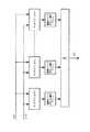
図3を参照すると、1.28Mcpsチップレートを利用する現行の3GPP仕様に従った無線通信システムとつないで使用するためのユーザ機器(UE)に適用することができる受信機の一部分のブロック図が示されている。UEは、(図示しない)アンテナを介して無線信号を受信し、少なくとも1.28Mcpsのチップレートを使用してその信号をサンプリングする。好ましくは、サンプリングは、チップレートの2倍の速度、またはチップレートの何らかの他の倍数の速度で行われる。チップレートより高いサンプリングレートにより、パフォーマンスが向上するが、余りにも高いサンプリングレートは、十分な処理速度を維持するために追加の処理機器のコストを要する可能性がある。サンプリングがチップレートの2倍の速度で行われる場合、当技術分野で周知のとおり、様々な処理オプションが利用可能である。例えば、別のサンプルが、2つの異なるデータストリームとして独立に処理されることが可能であり、あるいはまた、サンプルを、従来の方法に従って選択的に組み合わせることが可能である。 Referring to FIG. 3, a block diagram of a portion of a receiver that can be applied to a user equipment (UE) for use in conjunction with a wireless communication system in accordance with current 3GPP specifications that utilize a 1.28 Mcps chip rate. It is shown. The UE receives a radio signal via an antenna (not shown) and samples the signal using a chip rate of at least 1.28 Mcps. Preferably, sampling is done at a rate twice the chip rate, or some other multiple of the chip rate. A sampling rate higher than the chip rate improves performance, but a sampling rate that is too high may require additional processing equipment costs to maintain sufficient processing speed. When sampling is performed at twice the chip rate, various processing options are available, as is well known in the art. For example, another sample can be processed independently as two different data streams, or alternatively, the samples can be selectively combined according to conventional methods.
図3に示す同期処理回路は、3GPP規格の1.28Mcpsオプションのフレームフォーマットに従って、基地局によって送信された通信信号のタイミングに関する情報を生成して、UEが基地局と通信することを可能にするように設計されている。前述したシーケンスS1のような、SYNC−DLコードの適切な変調シーケンスが検出された場合、UEは、スーパーフレームのタイムスロット0内のP−CCPCHで伝送されるブロードキャストチャネル(BCH)内の、基地局によって送信されたデータを読み取ることができ、このデータにより、UEは、そのBCHデータを送信した基地局と双方向通信を行うことができるようになる。同期処理回路は、次の3つの主な構成要素を有する。すなわち、SYNC−DL決定回路10、ミッドアンブル決定回路20、および位相変調シーケンス検出回路30である。 The synchronization processing circuit shown in FIG. 3 generates information regarding the timing of communication signals transmitted by the base station according to the frame format of the 1.28 Mcps option of the 3GPP standard, and enables the UE to communicate with the base station. Designed to be If an appropriate modulation sequence of the SYNC-DL code, such as the sequence S1 described above, is detected, the UE will be able to access the base in the broadcast channel (BCH) transmitted on the P-CCPCH in time slot 0 of the superframe. The data transmitted by the station can be read, and this data enables the UE to perform bi-directional communication with the base station that transmitted the BCH data. The synchronization processing circuit has the following three main components. That is, the SYNC-DL determination circuit 10, the
SYNC−DL決定回路10は、検出回路13に相関データを出力する複数のM個の並列マッチドフィルタ/相関器121ないし12Mを含む。受信される通信信号サンプルは、相関器121ないし12Mのそれぞれに入力される。また、各相関器121ないし12Mは、各相関器121ないし12Mが処理中のサンプルのセットを32の異なるSYNC−DLコードの1つと相関させることを可能にする同期コードジェネレータ11からの入力も有する。The SYNC-DL determination circuit 10 includes a plurality of M parallel matched filters / correlators 121 to 12M that output correlation data to the
現在の規格の1.28Mcpsオプションでは、各SYNC−DLコードは、64の要素を有し、したがって、相関器121ないし12Mは、一度に64の受信信号サンプルのセットを処理するように構成されている。図4に示すとおり、相関器121ないし12Mの各相関器は、好ましくは、関連するスクエアリング(squaring)デバイスまたは同様のデバイス、および加算器をそれぞれが有するN個のマッチドフィルタのバンクとして構成される。各マッチドフィルタは、64の受信信号サンプルのセットの長さの内の64/Nの異なるセグメントを処理する。SYNC−DLコードの対応するセグメントは、マッチドフィルタのそれぞれのコード入力に導かれる。各マッチドフィルタは、それぞれのスクエアリングデバイスまたは同様のデバイスに信号を出力する出力を有し、このデバイスは集合として加算器に信号を出力し、加算器は、集合的なセグメント出力を加算して相関器の出力を提供する。In 1.28Mcps option for the current standards, each SYNC-DL code has an element 64, thus, to 12M correlators 121, configured to process the set of received signal samples of 64 at a time Has been. As shown in FIG. 4, each correlator of correlators 121 to 12M is preferably as a bank of N matched filters, each with an associated squaring device or similar device, and an adder. Composed. Each matched filter processes 64 / N different segments of the length of the set of 64 received signal samples. The corresponding segment of the SYNC-DL code is routed to the respective code input of the matched filter. Each matched filter has an output that outputs a signal to a respective squaring device or similar device, which outputs the signal to the adder as a set, and the adder adds the collective segment outputs. Provides the output of the correlator.
相関器121ないし12Mは、第1の入力速度で信号サンプルを受け取るが、より速い速度で動作するので、各相関器は、少なくとも2つの異なるSYNC−DLコードに関する相関データを出力してから、後続の信号サンプルの処理を行うことができる。例えば、図4を参照すると、所与のサンプル入力速度(ir)に対して、SYNC−DLコードジェネレータ11からのコード入力速度は、N個のマッチドフィルタのそれぞれについて、ir周期ごとに少なくとも8つのコード要素である。各々対応するSYNC−DLコードの4つの要素のセットがN個のマッチドフィルタのそれぞれによって受け取られた後、相関データ出力が2乗され、全体として合計されて、出力される。各相関器121ないし12Mは、サンプル入力速度周期ごとに少なくとも2つのSYNC−DLコードを処理するので、重大な処理遅延を全く被ることなく必要とされる相関器の数Mは、可能なコードの数の半分を超えない。Correlators 121 to 12M receive signal samples at a first input rate, but operate at a faster rate so that each correlator outputs correlation data for at least two different SYNC-DL codes. Subsequent signal sample processing can be performed. For example, referring to FIG. 4, for a given sample input rate (ir), the code input rate from the SYNC-
好ましい構成では、各相関器121ないし12Mは、好ましくは、サンプル入力速度周期ごとに4つのSYNC−DLコードを処理する速度で動作し、したがって、8個(M=8)の相関器が使用される。すなわち、可能なコードの数(32)を速度係数(4)で割った数である。好ましい実施形態では、各相関器は、長さ8の8個(N=8)のマッチドフィルタから構成される。すなわち、コードの長さ(64)をセグメントの数(8)で割った数である。要素処理の点からは、処理される信号サンプルの各要素に関して、各マッチドフィルタによってSYNC−DLコードの16の要素が処理される。In a preferred arrangement, the correlators 121 to 12M is preferably operated at a speed which processes four SYNC-DL codes per sample input rate period, therefore, the correlator eight (M = 8) used. That is, the number of possible codes (32) divided by the speed factor (4). In the preferred embodiment, each correlator is composed of8 (N =8 ) matched filters of length8 . That is, the number obtained by dividing the code length (64) by the number of segments (8 ). In terms of element processing, for each element of the signal sample being processed, each matched filter processes 16 elements of the SYNC-DL code.
検出回路13は、相関器121ないし12Mから出力を受け取り、選択された数のフレームにわたって正の相関を追跡する。また、通信信号サンプルを受け取り、ノイズ推定を出力するノイズ推定回路15が提供される。検出回路13は、ノイズ推定回路15からのノイズ推定を使用して、相関器121ないし12Mの1つからの出力が正であるか否かを判定する。好ましくは、正の相関は、SYNC−DLコード相関に関する相関器出力が選択されたノイズ係数の定数が掛けられたノイズ推定を超えた場合に検出される。
同一のSYNC−DLコードにより、複数の、好ましくは8つの、サブフレームにわたる同じ相対位置で正の相関が生成された場合、検出回路により、受け取られている特定のSYNC−DLと通信信号内のDwPTSの相対位置がともに識別されたと決定され、その相対位置により、サブフレームのそれぞれのタイムスロット0の位置、および関連するミッドアンブルが提供される。 If the same SYNC-DL code generates a positive correlation at the same relative position across multiple, preferably eight, subframes, the detection circuit will receive the specific SYNC-DL and communication signal in It is determined that the relative position of DwPTS has been identified together, and that relative position provides the position of each time slot 0 of the subframe and the associated midamble.
好ましくは、ミッドアンブル検出回路20のバッファ21に送り込まれる入力信号の周波数を調整するように検出回路13によって制御される自動周波数制御(AFC)回路16が提供される。AFCの出力は、ミキサー17を介して信号サンプル入力とミキシングされて、周波数調整されたサンプル入力をミッドアンブル検出回路に提供する。後続のステップが整合のとれた処理を行うことができるように、AFC、搬送波再生は、SYNC−DLコード決定と併せて完了することが可能である。SYNC−DLコードの肯定的な検出毎に、検出回路は、制御信号をAFC16に送る。AFCプロセスは、検出回路13によるSYNC−DLの決定が完了した時点で完了する。あるいはまた、ミキサー17をSYNC−DL決定回路10の入力に配置して、回路10が決定機能を続行している間に受け取る入力信号にAFC訂正が行われるようにすることも可能である。ミキサー17に関するこの代替の位置は、シーケンス決定回路30に対する入力よりも前段である。 Preferably, an automatic frequency control (AFC)
SYNC−DL決定回路10は、32のSYNC−DLコードのどれが、基地局から受信されているかを決定すると、ミッドアンブル選択回路が、4つの基本ミッドアンブルのどれが、受信SYNC−DLコードを送信した基地局によって伝送されたP−CCPCH内で利用されているかを決定するように動作することができる。現在の規格の3GPPシステムでは、P−CCPCHは、サブフレームのタイムスロット0の最初の2つのコードチャネルにマップされた2つのチャネルP−CCPCH1およびP−CCPCH2から構成される。 When the SYNC-DL determination circuit 10 determines which of the 32 SYNC-DL codes are received from the base station, the midamble selection circuit determines which of the four basic midambles receives the received SYNC-DL code. It can operate to determine if it is used in the P-CCPCH transmitted by the transmitting base station. In the current standard 3GPP system, the P-CCPCH consists of two channels P-CCPCH1 and P-CCPCH2 mapped to the first two code channels in time slot 0 of the subframe.
ミッドアンブル選択回路20は、SYNC−DL決定回路10の検出回路13からSYNC−DLコード識別および相対タイミング情報を受け取るミッドアンブルジェネレータを含む。次に、ミッドアンブルジェネレータ23が、検出回路13によって前に識別されているSYNC−DLコードに関連する4つの128ビットのミッドアンブルの各々から144ビットのミッドアンブルを生成する。DwPTSの相対位置が決定されると、連続するタイムスロット0のミッドアンブルの位置に対応するサンプルが、バッファ21から、P−CCPCH1を表す第1のコードチャネルに関するマッチドフィルタ/相関器24a、および第2のコードチャネルP−CCPCH2を表す24bに入力される。これらの入力は、識別されたSYNC−DLコードに対応する4つの基本ミッドアンブルのそれぞれから導出されたミッドアンブルジェネレータ23からの入力に相関させられる。判断回路26は、4つのミッドアンブルのどれが基地局によって伝送されたかを識別するために、マッチドフィルタ/相関器24aおよび24bからのミッドアンブルの各反復比較の相関を受け取る。好ましくは、この決定は、第2の選択された相関係数の定数が掛けられたノイズ推定器15から受け取られたノイズ推定と比較して行われる。
マッチドフィルタ/相関器121ないし12Mは、ミッドアンブル検出回路20がミッドアンブルを決定している最中にSYNC−DL決定回路10によって使用される必要はない。したがって、ミッドアンブル検出回路20は、マッチドフィルタ/相関器24aおよび24bとしてマッチドフィルタ/相関器121ないし12Mを使用するように構成することが可能である。ハードウェアの再使用により、効率的な実装が提供される。The matched filter / correlator 121 to 12M need not be used by the SYNC-DL determination circuit 10 while the
また、2つのマッチドフィルタ/相関器24aおよび24bを使用することは、P−CCPCHで使用することが可能な時空間符号化送信ダイバーシチに対応することができる。その場合、通常の動作における1つのミッドアンブルの1/2の電力で2つのミッドアンブルが使用される。両方のミッドアンブルの検出が行われ、決定デバイスが両方のミッドアンブルを非コヒーレントの形で結合する。Moreover, the use of two matched filter / correlator 24a and 24b may correspond to a spatial coding transmit diversity when it can be used in P-CCPCH. In that case, two midambles are used at half the power of one midamble in normal operation. Both midambles are detected and the decision device combines both midambles in a non-coherent manner.
肯定的なミッドアンブル決定が行われた場合、判断回路26が、ミッドアンブルジェネレータ23にミッドアンブル選択信号を出力し、ミッドアンブルジェネレータ23は、識別されたミッドアンブルをシーケンス検出回路30に出力する。 When a positive midamble determination is made, the
シーケンス検出回路30は、信号サンプルを受け取るバッファ31、変調相関器32、および判断回路34を含む。ミッドアンブル決定回路のバッファ21は、バッファ31として再使用することが可能であり、その場合、シーケンス検出回路は、前述したミキサー17の配置変更なしにAFCを活用する。 The
シーケンス検出回路30は、SYNC−DL決定回路10の検出回路13から、識別されたSYNC−DLコードとDwPTS位置情報とを受け取り、および、ミッドアンブル検出回路20からミッドアンブルデータを受け取る。変調相関器32は、受信された通信サンプルが中に格納されているバッファ31から入力を受け取り、判断回路34にデータを出力する。相関器32は、DwPTS内のSYNC−DLコードのQPSK変調を一連のサブフレームの識別されたミッドアンブルに相関させる。この情報は、判断回路34に出力される。別々の相関器が提供されて、SYNC−DLコードの位相、およびミッドアンブルコードの位相をそれぞれ検出する。あるいはまた、単一の相関器が共用されて、SYNC−DLとミッドアンブルコードの両方の位相を検出することも可能である。 The
判断回路34が、決定されたミッドアンブルと4つまたはそれより多くの連続するSYNC−DLコードとの間の位相効果を計算する。判断回路34は、前述したS1シーケンスのような選択されたシーケンスが検出されたか否かを決定する。選択された変調シーケンスが検出された場合、判断回路34は、スーパーフレームタイミング(SFT)を出力し、タイムスロット0内のP−CCPCHでBCHデータが伝送されるスーパーフレームの先頭を特定する。これは、DwPTSの変調のS1シーケンスに続く次のスーパーフレームとして3GPPにおいて現在、規定されている。A decision circuit 34 calculates the phaseeffect between the determined midamble and four or more consecutive SYNC-DL codes. The decision circuit 34 determines whether a selected sequence such as the S1 sequence described above has been detected. When the selected modulation sequence is detected, the determination circuit 34 outputs the superframe timing (SFT) and specifies the head of the superframe in which the BCH data is transmitted on the P-CCPCH in the time slot 0. This is currently defined in 3GPP as the next superframe following the S1 sequence of DwPTS modulation.
Claims (18)
Translated fromJapanese受信された通信信号サンプルを処理するための同期回路を備え、
前記同期回路は、前記チップレートと少なくとも同じ入力速度でサンプルを受け取り、前記サンプル入力速度より速い処理速度で連続するY個のサンプルのセットを処理する同期コード決定回路を有し、
前記同期コード決定回路は、
さらなる通信信号サンプルを処理する前に、受信された通信信号サンプルを前記サンプル入力速度で並列に受け取り、連続するY個のサンプルのセットの各々をX個のダウンリンク同期コードのセットの少なくとも2つの同期コードに相関させるための入力を有するM≦X/2である複数のM個のY要素相関器と、
前記相関器に動作上、関連付けられて連続するY個のサンプルセットの各々とのダウンリンク同期コードの正の相関を検出し、追跡する検出回路とを含み、
前記相関器のそれぞれは、並列な複数のN個のマッチドフィルタを含み、前記サンプル入力速度の少なくとも2倍の速度で連続するY個のサンプルの各セットに関する符号相関を出力して、前記相関器が集合として、連続するY個のサンプルのセットについてすべてのX個の同期コードに関する相関データを前記検出回路に出力してから、さらなる通信信号サンプルが処理されるようにするための出力を有し、
前記マッチドフィルタの各々が、1入力期間で、前記受け取った通信信号サンプルのうちのY/N個の要素セグメントを前記X個のダウンリンク同期コードのセットの少なくとも2つの同期コードのうちの対応するY/N個の要素セグメントと相関させるマッチドフィルタである
ことを特徴とするユーザ機器(UE)。In a downlink pilot time slot, the base station transmits a synchronization code selected from predetermined X downlink synchronization codes consisting of Y consecutive elements, where X and Y are integers greater than 15 at a predetermined chip rate. User equipment (UE) for use in a wireless communication system utilizing a time frame format, wherein the user equipment receives a communication signal and samples the received communication signal at a sampling rate at least the chip rate. ) And
A synchronization circuit for processing received communication signal samples;
The synchronization circuit includes a synchronization code determination circuit that receives samples at an input speed at least as high as the chip rate and processes a set of consecutiveY samples at a processing speed faster than the sample input speed;
The synchronization code determination circuit includes:
Prior to processing further communication signal samples, received communication signal samples are received in parallel at the sample input rate,and eachsuccessive setofY samples is taken into at least two of the set of X downlink synchronization codes. A plurality of M Y-element correlators with M ≦ X / 2 having inputs for correlating to the synchronization code;
A detection circuit that detects and tracks a positive correlation of a downlink synchronization code witheachof the consecutiveY sample sets operatively associated with the correlator;
Each of the correlators includes aplurality of N matched filters in parallel and outputs a code correlation for each set ofY samplesconsecutive at a rate of at least twice the sample input rate;has but as a set, the correlation data for all X number of synchronization codes from the output to the detection circuitfor a set of Y-number of consecutive samples the output so that further communication signal samples are processed,
Each of the matched filters corresponds to Y / N element segments of the received communication signal samples in one input period corresponding to at least two synchronization codes of the set of X downlink synchronization codes. User equipment (UE), characterized in thatit is a matched filter that correlates with Y / N element segments .
前記同期コード決定回路に動作上、関連付けられ、検出されたダウンリンク同期コードの相対位置および識別に基づいて前記それぞれの伝送されたミッドアンブルを決定するミッドアンブル決定回路と、
前記ミッドアンブル決定回路および前記同期コード決定回路に動作上、関連付けられ、前記同期コード決定回路によって検出されたダウンリンク同期コード、および前記ミッドアンブル決定回路によって決定されたミッドアンブルに基づいて連続する検出されたダウンリンク同期コードの位相変調のシーケンスを決定する位相変調シーケンス検出回路とをさらに含むことを特徴とする請求項2に記載のUE。The UE receives the data of the specified channel (BCH) transmitted on the primary common control physical channel (P-CCPCH) in the selected time slot of the predefined system time frame structure, and the UE transmits the BCH data A continuous downlink synchronization code that allows two-way communication with a base station, each transmitted downlink synchronization code having a modulation indicated by a midamble transmitted in a defined time slot The specified modulation sequence identifies the location of BCH data, and the UE
A midamble determination circuit that is operatively associated with the synchronization code determination circuit and determines the respective transmitted midamble based on the relative position and identification of the detected downlink synchronization code;
Continuous detection based on the downlink synchronization code operatively associated with the midamble determination circuit and the synchronization code determination circuit and detected by the synchronization code determination circuit, and the midamble determined by the midamble determination circuit The UE according to claim 2, further comprising a phase modulation sequence detection circuit for determining a phase modulation sequence of the downlink synchronization code generated.
前記ノイズ推定回路は、同期コード検出が依拠するノイズ推定を前記検出回路に提供し、
前記検出回路は、前記AFCを制御して、前記ミッドアンブル決定回路に入力される受信された通信サンプルとミキシングされる周波数訂正信号を生成することを特徴とする請求項6に記載のUE。The synchronization code determination circuit includes a noise estimation circuit and an automatic frequency control circuit (AFC) associated with the detection circuit;
The noise estimation circuit provides the detection circuit with a noise estimate upon which synchronization code detection is relied upon;
The UE according to claim 6, wherein the detection circuit controls the AFC to generate a frequency correction signal mixed with the received communication sample input to the midamble determination circuit.
前記ミッドアンブル決定回路は、バッファと、少なくとも1つのミッドアンブル相関器と、ミッドアンブルジェネレータと、ミッドアンブル判断回路とを含み、
前記バッファは、前記同期コード決定回路から、AFC訂正された通信信号サンプルを受け取るための入力を有し、
前記ミッドアンブルジェネレータは、前記同期コード決定回路から前記決定された同期コードを受け取るための入力を有し、前記特定された同期コードが示すミッドアンブルの前記事前定義されたセットに基づいてミッドアンブルを順次に生成し、
前記ミッドアンブル相関器は、前記規定のタイムスロットのミッドアンブル部分に対応する前記バッファからの通信信号サンプルのセットを受け取るための入力、前記ミッドアンブルジェネレータから生成されたミッドアンブルを受け取るための入力、および前記ミッドアンブル判断回路に相関データを出力するための出力を有し、および
前記ミッドアンブル判断回路は、前記決定された同期コードが示すミッドアンブルの前記事前定義されたセットの前記ミッドアンブルのどれが前記決定された同期コードとともに伝送されたかを、前記規定のタイムスロットのミッドアンブル部分に対応する前記バッファからの通信信号サンプルのセットと前記ミッドアンブルジェネレータからの生成されたミッドアンブルとの間の相関データに基づいて決定し、および前記ミッドアンブルジェネレータに選択信号を出力するための出力を有し、前記ミッドアンブルジェネレータが、前記選択信号に基づくミッドアンブルを前記位相変調シーケンス検出回路に出力する出力を有する
ことを特徴とする請求項7に記載のUE。Each synchronization code represents a predefined set of midambles, one transmitted with each transmitted downlink synchronization code, indicating the modulation of that transmitted code,
The midamble determination circuit includes a buffer, at least one midamble correlator, a midamble generator, and a midamble determination circuit;
The buffer has an input for receiving AFC corrected communication signal samples from the synchronization code determination circuit;
The midamble generator has an input for receiving the determined synchronization code from the synchronization code determination circuit, and based on the predefined set of midambles indicated by the identified synchronization code Are generated sequentially,
The midamble correlator has an input for receiving a set of communication signal samples from the buffer corresponding to a midamble portion of the prescribed time slot; an input for receiving a midamble generated from the midamble generator; And an output for outputting correlation data to the midamble determining circuit, and the midamble determining circuit is configured for the midamble of the predefined set of midambles indicated by the determined synchronization code. Which was transmitted with the determined synchronization code, between the set of communication signal samples from the buffer corresponding to the midamble portion of the prescribed time slot and the generated midamble from the midamble generator Based on the correlation data of And an output for outputting a selection signal to the midamble generator, the midamble generator having an output for outputting a midamble based on the selection signal to the phase modulation sequence detection circuit. The UE according to claim 7.
前記位相変調シーケンス検出回路のバッファは、前記同期コード決定回路から通信信号サンプルを受け取るための入力を有し、
前記位相相関器手段は、前記受信された通信信号サンプルの同期コード部分に対応する前記位相変調シーケンス検出回路のバッファからの通信信号サンプルのセットと、前記ミッドアンブルジェネレータからの選択されたミッドアンブルとを受け取り、前記シーケンス判断回路に位相相関データを出力し、および
前記決定された同期コードに対応する通信信号サンプルの連続するセットの位相シーケンスを識別する前記シーケンス判断回路は、前記位相相関器手段から位相相関データを受け取るための入力を有し、規定の位相シーケンスが検出された場合、前記BCHデータの位置を識別する信号を出力するための出力を有する
ことを特徴とする請求項8に記載のUE。The phase modulation sequence detection circuit includes a buffer, phase correlator means, and a phase sequence determination circuit,
A buffer of the phase modulation sequence detection circuit has an input for receiving a communication signal sample from the synchronization code determination circuit;
The phase correlator means includes a set of communication signal samples from a buffer of the phase modulation sequence detection circuit corresponding to a synchronization code portion of the received communication signal samples, and a selected midamble from the midamble generator; The sequence determination circuit is configured to output phase correlation data to the sequence determination circuit and identify a phase sequence of successive sets of communication signal samples corresponding to the determined synchronization code from the phase correlator means 9. The input according to claim 8, comprising an input for receiving phase correlation data, and an output for outputting a signal identifying a position of the BCH data when a prescribed phase sequence is detected. UE.
M≦X/2である複数のM個のY要素相関器であって、それぞれ並列な複数のN個のマッチドフィルタを含む相関器を有する同期コード決定回路で、前記チップレートと少なくとも同じ入力速度で、通信信号サンプルを受け取ること、および、前記サンプル入力速度より速い処理速度で、連続するY個のサンプルのセットを処理することを備え、該処理は、
さらに通信信号サンプルを処理する前に、前記サンプル入力速度で、前記相関器で並列に通信信号サンプルを受け取ること、および、連続するY個のサンプルのセットの各々をX個のダウンリンク同期コードのセットの少なくとも2つの同期コードと相関させること、
連続するY個のサンプルのセットの各々とダウンリンク同期コードとの前記相関器の正の相関を検出することおよび追跡すること、および
さらに通信信号サンプルを処理する前に、集合的に前記相関器がすべてのX個の同期コードに関する相関データを出力するように、少なくとも前記サンプル入力速度の2倍の速度で、連続するY個のサンプルのセットの各々に関して、前記相関器の各々から符号相関を出力すること
を含み、
前記マッチドフィルタの各々が、1入力期間で、前記受け取った通信信号サンプルのうちのY/N個の要素セグメントを前記X個のダウンリンク同期コードのセットの少なくとも2つの同期コードのうちの対応するY/N個の要素セグメントと相関させるマッチドフィルタである
ことを特徴とする方法。In a downlink pilot time slot, the base station transmits a synchronization code selected from predetermined X downlink synchronization codes consisting of Y consecutive elements, where X and Y are integers greater than 15 at a predetermined chip rate. A method for processing a received communication signal in a wireless communication system using a time frame format, wherein a downlink communication signal is received and sampled at a sampling rate at least the same as the chip rate, comprising: The method
A synchronization code determination circuit having a plurality of M Y-element correlators with M ≦ X / 2, each including aplurality of N matched filters in parallel, and an input speed at least equal to the chip rate Receiving a communication signal sample and processing a set of consecutiveY samples at a processing rate faster than the sample input rate, the processing comprising:
Receivingfurther communication signal samples at the correlator in parallel at the sample input rate, and processing each of a set ofconsecutive Y samples with X downlink synchronization codesbefore processing further communication signal samples. Correlating with at least two synchronization codes of the set;
Detecting and tracking a positive correlation of the correlator betweeneachof a setof consecutiveY samples and a downlink synchronization code; and further processing the communication signal samples collectively, the correlator Sign correlation from each of the correlatorsfor eachsuccessive setofY samples at least twice as fast as the sample input rate so that outputs correlation data for all X synchronization codes.look at including thatoutput,
Each of the matched filters corresponds to Y / N element segments of the received communication signal samples in one input period corresponding to at least two synchronization codes of the set of X downlink synchronization codes. A matched filter that correlates with Y / N element segments .
受信された通信信号サンプルを前記サンプル入力速度で並列に受け取り、サンプルの各セットを、1入力速度期間内に、32個のダウンリンク同期コードの前記セットの少なくとも4つの同期コードと相関させることを特徴とする請求項13に記載の方法。When the set is correlated, no more than 8 correlators are used, and each correlator is
Receiving received communication signal samples in parallel at the sample input rate and correlating each set of samples with at least four synchronization codes of the set of 32 downlink synchronization codes within one input rate period; 14. A method according to claim 13 characterized in that
前記方法は、
検出されたダウンリンク同期コードの相対位置および識別に基づいて、伝送されたミッドアンブルの各々を決定すること、および
検出されたダウンリンク同期コードおよび決定されたミッドアンブルに基づいて、連続する検出されたダウンリンク同期コードの位相変調のシーケンスを決定すること
備えたことを特徴とする請求項13に記載の方法。A base station that receives data of a specified channel (BCH) transmitted on a primary common control physical channel (P-CCPCH) in a selected time slot of a predefined system time frame structure and transmits the BCH data And each transmitted downlink synchronization code has a modulation indicated by a midamble transmitted in a specified time slot, and a specified modulation of consecutive downlink synchronization codes The sequence locates the BCH data,
The method
Determining each of the transmitted midambles based on the relative position and identification of the detected downlink synchronization code, and consecutively detecting based on the detected downlink synchronization code and the determined midamble. 14. The method of claim 13, comprising determining a phase modulation sequence of a downlink synchronization code.
前記相関させることの前に、自動周波数制御回路(AFC)を使用して、受信された通信サンプルとミキシングされる周波数訂正信号を生成すること
をさらに備えたことを特徴とする請求項17に記載の方法。A noise estimation circuit is used to generate a noise estimate on which synchronization code detection relies, and prior to the correlation, an automatic frequency control circuit (AFC) is used to mix the received communication samples. The method of claim 17, further comprising: generating a frequency correction signal.
Applications Claiming Priority (2)
| Application Number | Priority Date | Filing Date | Title |
|---|---|---|---|
| US32859001P | 2001-10-11 | 2001-10-11 | |
| PCT/US2002/032470WO2003032512A1 (en) | 2001-10-11 | 2002-10-10 | Acquisition circuit for low chip rate option for mobile telecommunication system |
Related Child Applications (1)
| Application Number | Title | Priority Date | Filing Date |
|---|---|---|---|
| JP2006324557ADivisionJP4291357B2 (en) | 2001-10-11 | 2006-11-30 | Acquisition circuit applicable to low chip rate option for mobile communication system |
Publications (3)
| Publication Number | Publication Date |
|---|---|
| JP2005506734A JP2005506734A (en) | 2005-03-03 |
| JP2005506734A5 JP2005506734A5 (en) | 2005-12-22 |
| JP4011545B2true JP4011545B2 (en) | 2007-11-21 |
Family
ID=23281594
Family Applications (2)
| Application Number | Title | Priority Date | Filing Date |
|---|---|---|---|
| JP2003535352AExpired - Fee RelatedJP4011545B2 (en) | 2001-10-11 | 2002-10-10 | Acquisition circuit applicable to low chip rate option for mobile communication system |
| JP2006324557AExpired - Fee RelatedJP4291357B2 (en) | 2001-10-11 | 2006-11-30 | Acquisition circuit applicable to low chip rate option for mobile communication system |
Family Applications After (1)
| Application Number | Title | Priority Date | Filing Date |
|---|---|---|---|
| JP2006324557AExpired - Fee RelatedJP4291357B2 (en) | 2001-10-11 | 2006-11-30 | Acquisition circuit applicable to low chip rate option for mobile communication system |
Country Status (14)
| Country | Link |
|---|---|
| US (5) | US6760365B2 (en) |
| EP (1) | EP1435139B9 (en) |
| JP (2) | JP4011545B2 (en) |
| KR (6) | KR100895660B1 (en) |
| CN (2) | CN1568582B (en) |
| AT (1) | ATE415740T1 (en) |
| AU (1) | AU2002347866B2 (en) |
| CA (1) | CA2463499C (en) |
| DE (2) | DE60230052D1 (en) |
| MX (1) | MXPA04003323A (en) |
| MY (1) | MY131068A (en) |
| NO (1) | NO20041746L (en) |
| TW (4) | TWI239727B (en) |
| WO (1) | WO2003032512A1 (en) |
Families Citing this family (38)
| Publication number | Priority date | Publication date | Assignee | Title |
|---|---|---|---|---|
| US6760365B2 (en)* | 2001-10-11 | 2004-07-06 | Interdigital Technology Corporation | Acquisition circuit for low chip rate option for mobile telecommunication system |
| US7356098B2 (en) | 2001-11-14 | 2008-04-08 | Ipwireless, Inc. | Method, communication system and communication unit for synchronisation for multi-rate communication |
| US7260056B2 (en)* | 2002-05-29 | 2007-08-21 | Interdigital Technology Corporation | Channel estimation in a wireless communication system |
| GB2396275B (en)* | 2002-12-09 | 2006-03-15 | Ipwireless Inc | Support of plural chip rates in a CDMA system |
| CN100438640C (en)* | 2002-12-30 | 2008-11-26 | Nxp股份有限公司 | Sampling method and its device for down synchronous tracking in TDD radio communication |
| SE0300443D0 (en)* | 2003-02-17 | 2003-02-17 | Ericsson Telefon Ab L M | Method and system of channel adaptation |
| CN1259785C (en)* | 2003-08-04 | 2006-06-14 | 大唐移动通信设备有限公司 | Method for obtaining carrier frequency departure of time division synchronous CDMA (TD-SCDMA) user terminal and equipment |
| WO2005029722A1 (en) | 2003-09-23 | 2005-03-31 | Koninklijke Philips Electronics N.V. | Initial synchronization for receivers |
| KR100548416B1 (en)* | 2003-10-28 | 2006-02-02 | 엘지전자 주식회사 | Wireless frame sync method |
| US7684372B2 (en) | 2004-05-04 | 2010-03-23 | Ipwireless, Inc. | Signaling MIMO allocations |
| US7722578B2 (en)* | 2004-09-08 | 2010-05-25 | Boston Scientific Scimed, Inc. | Medical devices |
| WO2006067658A2 (en)* | 2004-12-24 | 2006-06-29 | Koninklijke Philips Electronics N.V. | Method and apparatus for time slot synchronization in wireless communication system |
| CN1798118A (en)* | 2004-12-24 | 2006-07-05 | 展讯通信(上海)有限公司 | Method for estimating frequency deviation accurately in TD-SCDMA |
| CN100399847C (en)* | 2005-02-24 | 2008-07-02 | 大唐移动通信设备有限公司 | Method for measuring adjacent cell |
| CN1841966A (en)* | 2005-04-01 | 2006-10-04 | 展讯通信(上海)有限公司 | Downlink synchronization code modulation phase sequence judging method in cell search |
| JP4179418B2 (en)* | 2005-07-13 | 2008-11-12 | 京セラ株式会社 | Wireless receiver |
| CN1941669B (en)* | 2005-09-29 | 2012-07-25 | 上海原动力通信科技有限公司 | Method for inserting down public guide frequency |
| KR101137344B1 (en) | 2006-01-20 | 2012-04-19 | 엘지전자 주식회사 | Method and apparatus for estimating frame synchronization |
| US7450944B2 (en)* | 2005-11-03 | 2008-11-11 | Motorola, Inc. | Method and apparatus for base station synchronization |
| CN1983915B (en)* | 2006-04-07 | 2010-12-01 | 华为技术有限公司 | A method and device for obtaining a feedback signal |
| US8121229B2 (en)* | 2006-07-24 | 2012-02-21 | Industrial Technology Research Institute | Guard section length detection method and system |
| CN104387314B (en)* | 2007-12-03 | 2018-09-21 | 株式会社半导体能源研究所 | Carbazole derivates, and light-emitting component, luminescent device and electronic device using carbazole derivates |
| US8964788B2 (en)* | 2008-06-05 | 2015-02-24 | Qualcomm Incorporated | System and method of an in-band modem for data communications over digital wireless communication networks |
| US9083521B2 (en)* | 2008-06-05 | 2015-07-14 | Qualcomm Incorporated | System and method of an in-band modem for data communications over digital wireless communication networks |
| US8958441B2 (en) | 2008-06-05 | 2015-02-17 | Qualcomm Incorporated | System and method of an in-band modem for data communications over digital wireless communication networks |
| US8725502B2 (en)* | 2008-06-05 | 2014-05-13 | Qualcomm Incorporated | System and method of an in-band modem for data communications over digital wireless communication networks |
| US8825480B2 (en) | 2008-06-05 | 2014-09-02 | Qualcomm Incorporated | Apparatus and method of obtaining non-speech data embedded in vocoder packet |
| CN101615922B (en)* | 2008-06-24 | 2012-12-05 | 中兴通讯股份有限公司 | Downlink synchronous tracking method and downlink synchronous tracking device |
| US8743864B2 (en)* | 2009-06-16 | 2014-06-03 | Qualcomm Incorporated | System and method for supporting higher-layer protocol messaging in an in-band modem |
| US8855100B2 (en)* | 2009-06-16 | 2014-10-07 | Qualcomm Incorporated | System and method for supporting higher-layer protocol messaging in an in-band modem |
| WO2011025333A2 (en)* | 2009-08-28 | 2011-03-03 | 엘지전자 주식회사 | Method in which a mobile terminal transmits/receives a signal using a predetermined tdd frame structure in a wireless communication system |
| CN102084693A (en)* | 2009-12-09 | 2011-06-01 | 高通股份有限公司 | Method and apparatus to determine intra-node-B cells in TD-SCDMA systems |
| WO2011071557A1 (en)* | 2009-12-09 | 2011-06-16 | Qualcomm Incorporated | Method and apparatus to determine intra-node-b cells in td-scdma systems |
| US8837644B2 (en)* | 2012-06-29 | 2014-09-16 | Blackberry Limited | Method and apparatus of cross-correlation with application to channel estimation and detection |
| CN103051356B (en)* | 2013-01-21 | 2015-08-12 | 中兴通讯股份有限公司 | CDMA communication system reduces the method and apparatus of the error rate |
| KR101463142B1 (en)* | 2013-02-15 | 2014-12-04 | 우리로광통신주식회사 | Automotive radar and operating method for the same |
| US9755881B1 (en)* | 2015-07-28 | 2017-09-05 | Marvell Israel (M.I.S.L) Ltd. | Receiver with data-aided automatic frequency control |
| CN106165805A (en)* | 2016-07-19 | 2016-11-30 | 张文全 | A kind of Quinoa beverage nourishing skin care and preparation method thereof |
Family Cites Families (30)
| Publication number | Priority date | Publication date | Assignee | Title |
|---|---|---|---|---|
| US5101416A (en) | 1990-11-28 | 1992-03-31 | Novatel Comunications Ltd. | Multi-channel digital receiver for global positioning system |
| JP3123196B2 (en) | 1992-04-16 | 2001-01-09 | 松下電器産業株式会社 | Demodulator for spread spectrum communication |
| US5592518A (en) | 1994-03-28 | 1997-01-07 | Hughes Electronics | Parallel frame synchronizer for detecting forward-ordered/reverse-ordered, inverted/non-inverted data |
| JP3120943B2 (en) | 1994-10-11 | 2000-12-25 | 松下電器産業株式会社 | CDMA receiver |
| US5822359A (en) | 1994-10-17 | 1998-10-13 | Motorola, Inc. | Coherent random access channel in a spread-spectrum communication system and method |
| JPH08195703A (en)* | 1995-01-17 | 1996-07-30 | Toshiba Corp | Wireless communication device |
| US5793772A (en) | 1995-11-29 | 1998-08-11 | Motorola, Inc. | Method and apparatus for synchronizing timing of components of a telecommunication system |
| US5973772A (en) | 1996-01-10 | 1999-10-26 | Kabushiki Kaisha Topcon | Layout judgment apparatus and layout judgment system |
| SE515911C2 (en)* | 1996-03-26 | 2001-10-29 | Ericsson Telefon Ab L M | Method and apparatus for receiving a symbol sequence |
| JPH10173630A (en) | 1996-12-13 | 1998-06-26 | Nec Corp | Cdma chip-synchronizing circuit |
| JP2902380B2 (en) | 1997-05-09 | 1999-06-07 | 株式会社ワイ・アール・ピー移動通信基盤技術研究所 | Parallel correlation processing circuit |
| JP3712156B2 (en) | 1997-09-30 | 2005-11-02 | ソニー株式会社 | Pseudo-noise code synchronization acquisition apparatus and reception apparatus |
| JP3793632B2 (en) | 1997-12-18 | 2006-07-05 | 松下電器産業株式会社 | Cell search method and mobile station apparatus |
| US6993084B1 (en) | 1998-04-14 | 2006-01-31 | Fraunhofer-Gesellschaft Zur Foerderung Der Angewandten Forschung E.V. | Coarse frequency synchronisation in multicarrier systems |
| ES2166161T3 (en) | 1998-04-14 | 2002-04-01 | Fraunhofer Ges Forschung | APPROXIMATE SYNCHRONIZATION OF FREQUENCIES IN MULTIPLE CARRIER SYSTEMS. |
| JP3397695B2 (en) | 1998-07-16 | 2003-04-21 | 松下電器産業株式会社 | Correlation detector and CDMA receiver |
| US6078607A (en)* | 1998-08-10 | 2000-06-20 | Omnipont Corporation | Synchronization codes for use in communication |
| US6141374A (en) | 1998-10-14 | 2000-10-31 | Lucent Technologies Inc. | Method and apparatus for generating multiple matched-filter PN vectors in a CDMA demodulator |
| DK1850497T3 (en)* | 1999-05-28 | 2010-12-13 | Interdigital Tech Corp | Cell Search Method for Time Split Duplex Communication Systems Using Code Split Multi-Citizen Access |
| US6363060B1 (en)* | 1999-06-30 | 2002-03-26 | Qualcomm Incorporated | Method and apparatus for fast WCDMA acquisition |
| JP2001077725A (en) | 1999-09-07 | 2001-03-23 | Sharp Corp | Correlator, matched filter, and terminal device using the matched filter |
| FI114887B (en)* | 1999-10-13 | 2005-01-14 | U Nav Microelectronics Corp | Signal detection system of a spread spectrum receiver |
| FI111109B (en) | 1999-12-09 | 2003-05-30 | Nokia Corp | Method for synchronizing a receiver, location system, receiver and electronic device |
| DE60014334T2 (en) | 2000-01-12 | 2005-10-13 | Mitsubishi Denki K.K. | Accelerated cell search in a mobile communication system |
| JP2001358532A (en) | 2000-06-13 | 2001-12-26 | Alps Electric Co Ltd | Voltage control oscillation circuit |
| TW518839B (en)* | 2000-08-30 | 2003-01-21 | Ind Tech Res Inst | Method and device of code group identification and frame edge synchronization |
| JP3741944B2 (en)* | 2000-09-18 | 2006-02-01 | 株式会社エヌ・ティ・ティ・ドコモ | Cell search method for mobile station in mobile communication system |
| AU770602B2 (en)* | 2000-10-05 | 2004-02-26 | Samsung Electronics Co., Ltd. | TSTD apparatus and method for a TDD CDMA mobile communication system |
| EP1241817A4 (en) | 2000-10-06 | 2003-01-22 | Yozan Inc | Receiver |
| US6760365B2 (en) | 2001-10-11 | 2004-07-06 | Interdigital Technology Corporation | Acquisition circuit for low chip rate option for mobile telecommunication system |
- 2002
- 2002-10-09USUS10/267,512patent/US6760365B2/ennot_activeExpired - Fee Related
- 2002-10-10MXMXPA04003323Apatent/MXPA04003323A/enactiveIP Right Grant
- 2002-10-10ATAT02784077Tpatent/ATE415740T1/ennot_activeIP Right Cessation
- 2002-10-10CACA002463499Apatent/CA2463499C/ennot_activeExpired - Fee Related
- 2002-10-10WOPCT/US2002/032470patent/WO2003032512A1/enactiveApplication Filing
- 2002-10-10JPJP2003535352Apatent/JP4011545B2/ennot_activeExpired - Fee Related
- 2002-10-10KRKR1020057015849Apatent/KR100895660B1/ennot_activeExpired - Fee Related
- 2002-10-10DEDE60230052Tpatent/DE60230052D1/ennot_activeExpired - Lifetime
- 2002-10-10KRKR1020077022978Apatent/KR20070106044A/ennot_activeWithdrawn
- 2002-10-10EPEP02784077Apatent/EP1435139B9/ennot_activeExpired - Lifetime
- 2002-10-10AUAU2002347866Apatent/AU2002347866B2/ennot_activeCeased
- 2002-10-10KRKR1020047005309Apatent/KR100790922B1/ennot_activeExpired - Fee Related
- 2002-10-10CNCN028201418Apatent/CN1568582B/ennot_activeExpired - Fee Related
- 2002-10-11TWTW091123441Apatent/TWI239727B/ennot_activeIP Right Cessation
- 2002-10-11CNCNU022873414Upatent/CN2674798Y/ennot_activeExpired - Lifetime
- 2002-10-11TWTW092127578Apatent/TWI260130B/ennot_activeIP Right Cessation
- 2002-10-11KRKR20-2002-0030440Upatent/KR200299433Y1/ennot_activeCeased
- 2002-10-11TWTW094135398Apatent/TWI296467B/ennot_activeIP Right Cessation
- 2002-10-11TWTW091216175Upatent/TWM240735U/ennot_activeIP Right Cessation
- 2002-10-11MYMYPI20023794Apatent/MY131068A/enunknown
- 2002-10-11DEDE20215686Upatent/DE20215686U1/ennot_activeExpired - Lifetime
- 2003
- 2003-12-10KRKR1020030089416Apatent/KR100585980B1/ennot_activeExpired - Fee Related
- 2004
- 2004-04-27USUS10/832,847patent/US7027495B2/ennot_activeExpired - Fee Related
- 2004-04-28NONO20041746Apatent/NO20041746L/ennot_activeApplication Discontinuation
- 2005
- 2005-08-18KRKR1020050075936Apatent/KR20050090099A/ennot_activeWithdrawn
- 2006
- 2006-02-13USUS11/352,570patent/US7403555B2/ennot_activeExpired - Fee Related
- 2006-11-30JPJP2006324557Apatent/JP4291357B2/ennot_activeExpired - Fee Related
- 2008
- 2008-07-21USUS12/176,850patent/US7627020B2/ennot_activeExpired - Fee Related
- 2009
- 2009-10-26USUS12/605,638patent/US8005129B2/ennot_activeExpired - Fee Related
Also Published As
Similar Documents
| Publication | Publication Date | Title |
|---|---|---|
| JP4011545B2 (en) | Acquisition circuit applicable to low chip rate option for mobile communication system | |
| AU2002347866A1 (en) | Acquisition circuit for low chip rate option for mobile telecommunication system | |
| KR100653228B1 (en) | A tdd node b using primary and secondary synchronization codes during cell search | |
| AU2006200703A1 (en) | Acquisition Circuit for Low Chip Rate Option for Mobile Telecommunication System | |
| HK1069688A (en) | Acquisition circuit for low chip rate option for mobile telecommunication system |
Legal Events
| Date | Code | Title | Description |
|---|---|---|---|
| A131 | Notification of reasons for refusal | Free format text:JAPANESE INTERMEDIATE CODE: A131 Effective date:20060530 | |
| A601 | Written request for extension of time | Free format text:JAPANESE INTERMEDIATE CODE: A601 Effective date:20060830 | |
| A602 | Written permission of extension of time | Free format text:JAPANESE INTERMEDIATE CODE: A602 Effective date:20060907 | |
| A521 | Request for written amendment filed | Free format text:JAPANESE INTERMEDIATE CODE: A523 Effective date:20061130 | |
| A02 | Decision of refusal | Free format text:JAPANESE INTERMEDIATE CODE: A02 Effective date:20070202 | |
| RD13 | Notification of appointment of power of sub attorney | Free format text:JAPANESE INTERMEDIATE CODE: A7433 Effective date:20070508 | |
| A521 | Request for written amendment filed | Free format text:JAPANESE INTERMEDIATE CODE: A523 Effective date:20070523 | |
| A521 | Request for written amendment filed | Free format text:JAPANESE INTERMEDIATE CODE: A821 Effective date:20070508 | |
| A911 | Transfer to examiner for re-examination before appeal (zenchi) | Free format text:JAPANESE INTERMEDIATE CODE: A911 Effective date:20070612 | |
| TRDD | Decision of grant or rejection written | ||
| A01 | Written decision to grant a patent or to grant a registration (utility model) | Free format text:JAPANESE INTERMEDIATE CODE: A01 Effective date:20070817 | |
| A61 | First payment of annual fees (during grant procedure) | Free format text:JAPANESE INTERMEDIATE CODE: A61 Effective date:20070905 | |
| R150 | Certificate of patent or registration of utility model | Free format text:JAPANESE INTERMEDIATE CODE: R150 | |
| FPAY | Renewal fee payment (event date is renewal date of database) | Free format text:PAYMENT UNTIL: 20100914 Year of fee payment:3 | |
| FPAY | Renewal fee payment (event date is renewal date of database) | Free format text:PAYMENT UNTIL: 20100914 Year of fee payment:3 | |
| FPAY | Renewal fee payment (event date is renewal date of database) | Free format text:PAYMENT UNTIL: 20110914 Year of fee payment:4 | |
| FPAY | Renewal fee payment (event date is renewal date of database) | Free format text:PAYMENT UNTIL: 20120914 Year of fee payment:5 | |
| FPAY | Renewal fee payment (event date is renewal date of database) | Free format text:PAYMENT UNTIL: 20130914 Year of fee payment:6 | |
| R250 | Receipt of annual fees | Free format text:JAPANESE INTERMEDIATE CODE: R250 | |
| LAPS | Cancellation because of no payment of annual fees |