JP4008047B2 - Semiconductor device - Google Patents
Semiconductor deviceDownload PDFInfo
- Publication number
- JP4008047B2 JP4008047B2JP19893394AJP19893394AJP4008047B2JP 4008047 B2JP4008047 B2JP 4008047B2JP 19893394 AJP19893394 AJP 19893394AJP 19893394 AJP19893394 AJP 19893394AJP 4008047 B2JP4008047 B2JP 4008047B2
- Authority
- JP
- Japan
- Prior art keywords
- layer
- metal oxide
- electrode
- capacitor
- electrode layer
- Prior art date
- Legal status (The legal status is an assumption and is not a legal conclusion. Google has not performed a legal analysis and makes no representation as to the accuracy of the status listed.)
- Expired - Lifetime
Links
Images


Classifications
- H—ELECTRICITY
- H10—SEMICONDUCTOR DEVICES; ELECTRIC SOLID-STATE DEVICES NOT OTHERWISE PROVIDED FOR
- H10B—ELECTRONIC MEMORY DEVICES
- H10B12/00—Dynamic random access memory [DRAM] devices
- H—ELECTRICITY
- H10—SEMICONDUCTOR DEVICES; ELECTRIC SOLID-STATE DEVICES NOT OTHERWISE PROVIDED FOR
- H10B—ELECTRONIC MEMORY DEVICES
- H10B12/00—Dynamic random access memory [DRAM] devices
- H10B12/30—DRAM devices comprising one-transistor - one-capacitor [1T-1C] memory cells
- H10B12/31—DRAM devices comprising one-transistor - one-capacitor [1T-1C] memory cells having a storage electrode stacked over the transistor
- H—ELECTRICITY
- H10—SEMICONDUCTOR DEVICES; ELECTRIC SOLID-STATE DEVICES NOT OTHERWISE PROVIDED FOR
- H10D—INORGANIC ELECTRIC SEMICONDUCTOR DEVICES
- H10D1/00—Resistors, capacitors or inductors
- H10D1/60—Capacitors
- H10D1/68—Capacitors having no potential barriers
- H10D1/682—Capacitors having no potential barriers having dielectrics comprising perovskite structures
Landscapes
- Semiconductor Memories (AREA)
- Semiconductor Integrated Circuits (AREA)
- Non-Volatile Memory (AREA)
Description
Translated fromJapanese【0001】
【産業上の利用分野】
本発明は、半導体デバイスの分野に関し、さらに詳しくは、コンデンサを有する半導体デバイスに関する。
【0002】
【従来の技術】
コンデンサは、多くの種類の半導体デバイスで用いられる。ダイナミック・ランダム・アクセス・メモリ(DRAM)セルまたは不揮発性ランダム・アクセス・メモリ(NVRAM)セルなどのメモリ・デバイス内では、コンデンサは蓄積コンデンサとして機能する。金属酸化物誘電層は、高誘電率または強誘電特性を有するので、DRAMまたはNVRAMセル用の蓄積コンデンサに利用できる。本明細書では、高誘電率(high permittivity) とは、二酸化シリコンの誘電率よりも高い誘電率を意味する。
【0003】
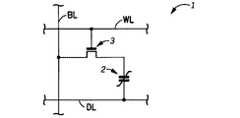
金属酸化物誘電層を用いたコンデンサの形成上の制限は、コンデンサの形成を半導体デバイスのプロセスの流れに組み込む実現性である。NVRAMセルを用いた特定の例は、いくつかの問題点を示す。図1は、強誘電コンデンサ2およびトランジスタ3を有するNVRAMセル1の回路図を含む。強誘電コンデンサ2の一方の電極は駆動ライン(DL)に結合され、他方の電極はトランジスタ3のソース/ドレイン領域に結合される。トランジスタ3は、ビット・ライン(BL)に結合された別のソース/ドレイン領域と、ワード・ライン(WL)に結合されたゲート電極とをさらに含む。
【0004】
ある従来のNVRAMセルは、「スタック形」強誘電コンデンサを含む。このNVRAMセルでは、トランジスタは基板に形成され、導電プラグはトランジスタのソース/ドレイン領域に形成され、強誘電コンデンサは導電プラグの上に形成される。集積上の問題点は、強誘電コンデンサが形成される際に導電プラグが存在することである。多くの種類の導電プラグには、シリコンまたは金属含有材料が含まれる。一般に、強誘電コンデンサの誘電層を形成する金属酸化物層は、金属酸化物層に強誘電特性を持たせるためには、摂氏約500度以上の高温で酸化しなければならない。本明細書では、高温とは、摂氏約500度以上の温度を意味する。導電プラグは、このような処理段階に耐えられないことがある。例えば、プラグは酸化して、導電性の低い領域を形成し、電極とその下のトランジスタのソース/ドレイン領域との間の電気経路を劣化または排除することがある。また別の例では、金属含有材料からの金属が基板内に拡散することがある。導電プラグの材料は、接合スパイク(junction spike)を形成するか、あるいはソース/ドレイン領域を完全に貫通するケイ化物を形成して、強誘電コンデンサの電極の1つと基板またはウェル領域との間で短絡を生じさせることがある。ほとんどの障壁層は摂氏約500度以上の処理に耐えられないので、障壁層も役に立たない。
【0005】
あるNVRAMセルでは、強誘電コンデンサが形成された後に、金属ストラップを強誘電層の電極とソース/ドレイン領域との間に形成することがある。図2は、トランジスタ93および強誘電コンデンサ95を含む「ストラップ形」NVRAMセル90の平面図を含む。金属導体91は、NVRAMセル90のビット・ラインとして機能し、ソース/ドレイン領域として機能する第1ドーピング領域931にコンタクト911によって電気接続される。導電部材92は、トランジスタ93のゲート電極として機能し、ワード・ラインの一部である。第2ドーピング領域932は、トランジスタ93の別のソース/ドレイン領域として機能し、導電部材92の他方の側面にある。トランジスタ93の能動領域は、フィールド絶縁領域98によって定められる。
【0006】
第1誘電層(図示せず)は、トランジスタ93が形成された後、かつ強誘電コンデンサ95を形成する前に形成される。一般に、強誘電コンデンサ95のほとんどは、フィールド絶縁領域98の上に形成される。強誘電コンデンサ95は、駆動ラインとして機能する低部電極層96と、強誘電体として機能する金属酸化物誘電層(図示せず)と、上部電極層97とを含む。第2絶縁層(図示せず)は、セル90の上に形成される。導電部材94は、強誘電コンデンサ95の上部電極層97を第2ドーピング領域932に対して電気接続する。金属導体91と導電部材94に現れる破線は、セルの下の要素が金属導体91または導電部材94の下にある場所を示している。少なくとも1つの絶縁層は、金属導体91または導電部材94と、破線によって示される下の要素との間にある。一般にコンタクト941,942,911は、同じ処理段階で形成され、コンタクトは少なくとも第2絶縁層を貫通することに留意されたい。さらに、導電部材91,94も一般に同じ処理段階で形成されることに留意されたい。
【0007】
【発明が解決しようとする課題】
NVRAMセル90は極めて大きい。セル寸法は、導電部材91,94を互いにどれほど近接して配置できるか、および/またはコンタクト941,942,911を互いにどれほど近接して配置できるかによって制限される。さらに、一般にアレイ上のビット・ラインの方向は、ワード・ラインとして機能する導電部材92に対して直交するので、セル寸法は大きくなる。従って、セルのビット・ラインとして機能する導電部材91の長さは、電気ストラップとして機能する導電部材94と一般に平行である。実質的に、トランジスタおよび強誘電コンデンサは、平面図から並んで形成される。コンタクト942がドーピング領域932に接触し、かつ強誘電コンデンサ95の低部または上部電極層96に接触しないように、十分な余裕を与えなければならないので、強誘電コンデンサは、トランジスタにわずかに重なるようにされる。
【0008】
同様な問題は、図3および図4に示すような他のNVRAMセルにも生じる。図3は、2つのトランジスタ31,33および2つの強誘電コンデンサ32,34を含むNVRAMセル30の回路図である。NVRAMセル30とNVRAMセル1との間の1つの違いは、1つのビット・ライン(BL)ではなく、相補形ビット・ライン(BLおよび反転BL)を用いることである。図4は、2つのpチャンネル・トランジスタ47,44と、2つのnチャンネル・トランジスタ42,45と、2つの強誘電コンデンサ43,46とを含むNVRAMセル40の回路図を含む。このセルとNVRAMセル1との間の相違点は、相補形ビット・ライン(BLおよび反転BL)と相補形ワード・ライン(WLおよび反転WL)とを用いることである。NVRAMセル30,40で用いられるスタック形強誘電コンデンサは、プロセス集積上の問題があり、ストラップ形セルは基板面積をとりすぎる。
【0009】
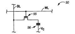
図5は、DRAMセル50の回路図を含む。DRAMセル50およびNVRAMセル90の回路図は同様である。DRAMセル50は、トランジスタ55および蓄積コンデンサ56を含む。ビット・ライン(BL)は、トランジスタ55のソース/ドレイン領域に結合される。トランジスタ55はさらに、ワード・ライン(WL)に結合されたゲート電極と、コンデンサ56の電極の1つに結合された別のソース/ドレイン領域とを含む。コンデンサ56の他方の電極は、定電圧源VC に結合される。セル50のVC は、VSSでも、あるいはVDDの電位の半分でもよい。
【0010】
小型化設計により、DRAMセルの蓄積コンデンサによって蓄積できる容量は制限される。厚さまたは寸法を増加せずに蓄積コンデンサの容量を増加する1つの方法として、金属酸化物誘電材料などの高誘電率誘電材料を利用する方法がある。残念ながら、金属酸化物誘電層を有する蓄積コンデンサには、NVRAMセルと同様な集積上の問題がある。金属酸化物誘電層の集積上の問題の多くは、二酸化シリコンおよび窒化シリコンなど従来のシリコン含有誘電材料にはない。
【0011】
【課題を解決するための手段】
本発明は、回路素子,コンデンサおよび導電部材によって構成される半導体デバイスを含む。コンデンサは回路素子の上にあり、第1電極層と、この第1電極層の上にある金属酸化物誘電層と、この誘電層の上にある第2電極層とを含む。導電部材は、回路素子および第2電極層を互いに電気接続し、導電部材がコンデンサの第1電極および誘電層を貫通するように構成される。本発明はさらに、このデバイスを製造する方法を含む。
【0012】
本発明の他の特徴および利点は、添付の図面と以下の詳細な説明から明らかになろう。
【0013】
本発明について、一例として説明し、添付の図面に限定されるものではない。ただし、同様な参照番号は同様な要素を表す。
【0014】
【実施例】
本発明は、コンデンサ自体を貫通する導電部材によって、下の回路素子に電気接続される電極層を有する金属酸化物コンデンサを含む。本発明は、DRAMまたはNVRAMに高誘電率または強誘電コンデンサを形成するのに特に役立つ。本発明の実施例について、以下で詳細に説明する。本発明は、説明する実施例に限定されない。
金属酸化物コンデンサ
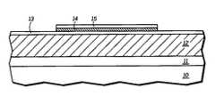
図6は、その上に形成された層を有する半導体基板10の一部の断面図を含む。回路素子11は、基板10の上にある。回路素子11は、基板10内のドーピング領域、または基板10の上にあるゲート電極,コンデンサ電極,コンタクトまたは穴プラグ(via plug)、相互接続などの導電部材を含むさまざまな要素の1つである。回路素子11は、形成される高誘電率金属酸化物コンデンサに電気接続される任意のものである。基板10は、半導体または絶縁材料でもよい。絶縁層12,低部電極層13,金属酸化物誘電層14および上部電極層15は、回路素子11の上に順次形成される。
【0015】
回路素子11の上の各層の材料の選択は、形成されるデバイスと、特定の層が現在またはその後接触する他の層とに依存する。例えば、DRAMは高誘電率コンデンサを必要とするが、金属酸化物誘電層14は強誘電特性を有する必要はない。金属酸化物層には、五酸化タンタル(Ta2 O5 ),チタン酸ジルコン(Zrx Tiy Oz ),チタン酸ストロンチウム(SrTiO3 ),チタン酸バリウム・ストロンチウム(BST),ジルコン酸チタン酸鉛(PZT),ジルコン酸チタン酸鉛ランタンなどが含まれる。チタン酸ジルコン鉛(lead zironium titanate)およびジルコン酸チタン酸鉛(lead zirconate titanate) は同じ材料であるが、この同一材料は2つの異なる名前を有する。NVRAMの場合、金属酸化物誘電層14は強誘電特性を有していなければならず、そのため、チタン酸ビスマス(Bi4 Ti3 O12),チタン酸バリウム(BaTiO3 ),BST,PZT,ジルコン酸チタン酸鉛ランタンなどを含んでもよい。
【0016】
電極層13,15の材料の選択は、誘電層14に用いられる材料に部分的に依存する。鉛は、多くのシリコン含有化合物と反応し、またはその中に拡散する。電極層13,15は、1)金属酸化物誘電層が鉛を含む場合、および2)誘電層14が摂氏約500度以上の温度にさらされる場合、シリコン含有化合物を含んだり、あるいは鉛の拡散を許してはならない。鉛がある場合、電極層13,15は、ルテニウム,レニウム,イリジウム,オスミウム,前記の4つの元素の導電金属酸化物のいずれか,プラチナなどを含んでもよい。金属酸化物誘電層がTa2 O5 を含む場合、電極層13,15はドーピング・シリコン,金属,金属含有化合物を含むほぼ任意の導電材料を含んでもよい。絶縁層12は、二酸化シリコン,窒化シリコンなどの任意の従来の半導体絶縁材料を含んでもよい。絶縁層12は、二酸化シリコン層と、二酸化チタンの薄い上層とを含む。別の実施例では、この薄い上層は必要なくても、あるいは五酸化タンタル,酸化マグネシウムなどを代わりにまたはこれらとともに用いてもよく、特に金属酸化物誘電層14が鉛を含み、かつ金属酸化物層14が高温処理中に絶縁層12と接触する可能性がある場合にそうである。また、絶縁層が薄い二酸化チタン層を含まない場合に、低部電極層13を形成する前に、薄いチタン層を形成してもよい。このチタン層は、絶縁層12と低部電極層13との間の接着層として機能する。もちろん、層12〜15の材料の選択は、デバイスの種類および特定の層に接触する層に依存する。
【0017】
わかりやすいように、強誘電コンデンサが形成されると想定する。具体的な材料は、本発明の理解を助けるために示される。本発明は、これら具体的な材料に限定されない。図6において、絶縁層12は二酸化シリコンであり、低部電極13はプラチナである。金属酸化物誘電層14はPZTであり、スパッタリング被着法,ゾル・ゲル・コーティング法または化学蒸着法などの従来の方法を用いて被着される。金属酸化物誘電層14は、摂氏約650〜700度の温度で、酸化雰囲気でアニールされる。アニール時間は、高速熱処理装置では約10〜300秒であり、従来の炉では約5〜30分である。酸化雰囲気は酸素を含み、窒素,ヘリウム,アルゴンなどの希釈ガスを含んでもよい。金属酸化物層14に用いられる材料および被着方法ならびに層14のアニール時間に応じて、アニール温度は摂氏約500〜800度でもよい。アニール後、プラチナからなる上部電極15が形成される。
【0018】
電極層13,15および金属酸化物層14は、従来の方法を用いてパターニングされる。本実施例では、プラチナは湿式エッチングまたは乾式エッチングされる。湿式エッチングは、王水溶液または改質王水溶液を用いて行うことができる。改質王水溶液は、塩酸(HCl)および硝酸(HNO3 )を含む水溶液であり、摂氏約75度のエッチング液である。エッチング液は、60〜80重量パーセントのリン酸H3 PO4 ,10〜25重量パーセントの酢酸(CH3 COOH),0.1〜5重量パーセントのHNO3 および残りの水を含む。このエッチング液は、Olin Hut Specialty Products, Inc社から市販されており、M2S (商標)という。乾式エッチングは、イオン・ミリング(ion milling) などの方法を用いて行うことができる。金属酸化物誘電層14は、湿式または乾式エッチング法を用いてパターニングできる。湿式エッチングは、フッ化水素酸,硝酸,および過酸化水素を含む溶液で行うことができる。この溶液は、エッチング中にほぼ室温で維持される。乾式エッチングは、プラズマ・エッチングまたはイオン・ミリングを用いて行うことができる。プラズマ・エッチングの場合、エッチング剤は、酸素,四フッ化炭素(CF4 )などのフッ素含有化合物,または四塩化炭素(CCl4 ),モル塩素(Cl2 )などの塩素含有化合物を含む。
【0019】
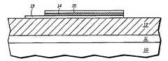
本実施例では、第1マスキング層(図示せず)は上部電極層15上に形成される。上部電極層15および金属酸化物誘電層14は、これら2つの層のエッジ部が互いに実質的に一致して、パターニング層を形成するように、イオン・ミリングを用いてパターニングされる。イオン・ミリング段階の次に、第1マスキング層は除去される。パターニングされた金属酸化物層14および上部電極層15を図7に示す。低部電極層13の一部は、イオン・ミリング中にエッチングできるが、図7に図示されていない。第2マスキング層(図示せず)は、電極層13,15上に形成される。低部電極層13は、プラチナで用いられる任意の湿式または乾式エッチングによってパターニングされる。低部電極層13がパターニングされた後、第2マスキング層は除去される。図8は、この段階におけるデバイスを示す。層14,15を越えて延在する低部電極層13の部分により、その後形成されるコンタクトは低部電極13に達することができる。
【0020】
開口部41は、図9に示すように、回路素子11まで層12〜15を貫通して形成される。第3マスキング層(図示せず)は、回路素子11までの開口部41が形成される上部電極層15上に形成される。開口部41は、層13〜15にイオン・ミリングを施し、次に絶縁層12にプラズマ・エッチングを施すことによって形成できる。イオン・ミリングにより、開口部に隣接する層のエッジ部を互いに実質的に一致させつつ、層13〜15をパターニングできる。イオン・ミリングは、部分的に絶縁層12まで進むことができる。一般に、絶縁層のプラズマ・エッチングは、イオン・ミリングに比べて、回路素子11に対して選択性の高いエッチングを行う。また、一般に、プラズマ・エッチングは、イオン・ミリングよりも高速に第3マスキング層を浸食しない。第3マスキング層が層12〜15のイオン・ミリングを見込んで十分厚い場合には、開口部41はイオン・ミリングで完全に形成できる。湿式エッチングまたは他の乾式エッチング方法など、他の従来のエッチング方法を用いて開口部41を形成できる。開口部41が形成された後、第3マスキング層は除去される。
【0021】
絶縁スペーサ51,52は、図10に示すように、層12〜15の露出されたエッジ部に沿って形成される。絶縁スペーサ51の材料の選択は、金属酸化物誘電層14に用いられる材料と、絶縁スペーサ51にその後施される温度サイクルとに依存する。本実施例では、デバイスが摂氏約500度以上の温度に露出される場合には、金属酸化物層14は、シリコン含有絶縁材料と反応する鉛(PZTから)を含む。従って、絶縁スペーサ51は、二酸化チタン(TiO2 ),五酸化タンタル(Ta2 O5 ),酸化マグネシウム(MgO)などを含んでもよい。
【0022】
スペーサ51,52を形成する1つの方法は、1)チタンを被着して、これを熱酸化して、二酸化チタンを形成し、2)フッ素含有プラズマを用いて二酸化チタンに異方性エッチングを施す。あるいは、スペーサ51,52は、反応性スパッタリングまたは化学蒸着法の次に異方性エッチングを施すことにより、TiO2 またはTa2 O5 を被着することによって形成できる。金属酸化物誘電層が鉛を含まず、あるいは摂氏約500度以上の温度にさらされない場合、スペーサ51,52にシリコン含有材料を利用できる。もちろん、多くの異なる材料や被着およびエッチング方法も利用できる。一般に、絶縁スペーサ51,52に用いられる材料の被着は、共形的(conformal) であるが、これは不可欠ではない。絶縁スペーサ51,52用の絶縁材料は、約100〜3000オングストロームの厚さに被着される。少なくとも絶縁材料の一部は、層13,14の露出された側端部に被着させなければならない。スペーサ51,52を形成するためのエッチングは、主に異方性でなければならない。このエッチングは、等方性エッチングを含んでもよいが、絶縁スペーサ51の少なくとも一部は層13,14に隣接しなければならない。絶縁スペーサ51の形成が完了すると、スペーサ51は、その後に開口部41内に形成される導電部材と、低部電極層13または金属酸化物誘電層14との間で電気接続を防ぐために十分な厚さでなければならない。
【0023】
導電部材61は、図11に示すように、回路素子11を上部電極層15に電気接続して形成される。導電部材61は、シリコン,金属または金属含有化合物を含んでもよい。一般に、導電層は、化学蒸着法,スパッタリング被着法などの従来の方法によって被着される。第4マスキング層(図示せず)は、導電部材61が形成される導電層の上に形成される。導電層の露出部分はエッチングされ、導電部材61を残す。第4マスキング層は、導電部材61が形成された後に除去される。多結晶シリコン,タングステンまたは窒化チタンは共形的に形成し、パターニングして、導電部材61を形成できる。あるいは、絶縁スペーサ51の側部に少なくとも一部の導電材料を残して、被着し、パターニングできる任意の導電材料を利用してもよい。
【0024】
導電部材は、2つ以上の部分を含んでもよい。例えば、開口部41を部分的または完全に埋める、タングステン,多結晶シリコンなどを含む導電プラグを形成してもよい。導電プラグと上部電極層15とを接触する局部相互接続も形成できる。この場合、導電プラグと局部相互接続との組合せが導電部材61を形成する。
【0025】
実質的に完成されたデバイスを図12に示す。第2絶縁層71は、導電部材61を含む基板10上に形成される。開口部および導電プラグ72は第2絶縁層71内で順次形成され、低部電極層13に電気接続を設ける。相互接続73およびパシベーション層74が形成される。他の層および電気接続(図示せず)も必要に応じて形成してもよい。
【0026】
本実施例において、多くの利点がわかる。コンデンサと、回路素子への接続には、貴重な基板面積をしめる従来のストラップがない。導電部材61は、高温処理のほとんどが終了してから形成される。従来のスタック形コンデンサでは、回路素子と低部電極との間の導電部材は、金属酸化物誘電層をアニールする前に形成された。従来のスタック形コンデンサの導電部材は、アニール中に隣接層または酸化雰囲気と反応,変形,融解,拡散などの都合の悪い相互作用を生じることがある。上記の本発明の実施例では、導電部材61は、金属酸化物誘電層14のアニール段階の後に形成される。従って、導電部材61は、アニール中に隣接層または酸化雰囲気と都合の悪い相互作用を生じることがない。導電部材61が導電金属酸化物または導電金属酸化物を形成できる金属であるならば、導電部材61が形成された後にデバイスを酸化雰囲気におくことができる。別の利点は、デバイス形成の簡素化である。プロセス集積上の問題は困難になるとは考えられない。
【0027】
金属酸化物誘電コンデンサを形成するあらゆる可能な代替方法の完全なリストを、作成するのは困難である。多くの代替方法についてすでに説明してきた。開口部41の部分を形成する前に層13〜15をパターニングすることは、多くの形態があり得る。各層13〜15を個別にパターニングしたり、層14を層13または層15とパターニングしたり、あるいは3つの層を一回でパターニングすることができる。また、開口部41の外側の層13〜15のパターニングは、導電部材61を形成した後に行うこともできる。絶縁スペーサ51,52を形成する絶縁層は、多くの異なる方法を用いて形成できる。この絶縁層は、化学蒸着またはスパッタリング被着(反応性またはその他)することができる。本実施例で説明したように、絶縁スペーサ51,52の絶縁層は、材料を被着して、次にこれを酸化して絶縁層を形成することによって形成できる。絶縁スペーサを形成するための酸化は、スペーサが形成された後に行ってもよい。この場合、回路素子11は、回路素子11とその後に形成される導電部材61との間に絶縁層を形成せずに、熱酸化サイクルに耐えることができなければならない。回路素子11を露出した後にスペーサ材料を酸化してスペーサ51,52を形成する場合、回路素子11は絶縁体を形成してはならない。具体的な厚さを示したが、本発明の精神または範囲から逸脱せずに他の厚さを用いてもよい。ここに示す代替方法は、例示的なもので本発明を制限するものではない。
NVRAMセル
本発明は、NVRAMセルで特に有効である。図13および図14は、トランジスタ103および強誘電コンデンサ105を有するNVRAMセル100を含む。図13はNVRAMセル100の平面図であり、図14はNVRAMセル100の断面図である。相互接続101はビット・ラインとして機能し、図13の左側と右側との間に延在する長さを有する。相互接続101の一部は、NVRAMセル100の下の要素をよりわかりやすく示すために、図13では図示されていない。導電プラグ1011は、トランジスタ103のソース/ドレイン領域として機能する第1ドーピング領域109に相互接続101を電気接続する。トランジスタ103はさらに、NVRAMセル100のワード・ラインとして機能する導電部材102と、トランジスタ103の別のソース/ドレイン領域として機能し、かつ強誘電コンデンサ105の下にある第2ドーピング領域(図13には図示せず)とを含む。強誘電コンデンサ105は、NVRAMセル100の駆動ラインとして機能する低部電極層106と、強誘電体として機能する金属酸化物誘電層(図13には図示せず)と、上部電極層107とを含む。導電部材117は、開口部104を介して上部電極層107をトランジスタ103の第2ドーピング領域に電気接続する。導電部材117は、強誘電コンデンサ105の低部電極層106または金属酸化物誘電層のいずれにも電気接続されない。図13は、トランジスタ103の能動領域を定めるフィールド絶縁領域108を含む。
【0028】
図14は、図13に示すNVRAMセル100の一部の断面図を含む。この断面図の説明は、セルの要素が形成される順番に従って行う。NVRAMセル100は、領域110上に形成される。この領域110は、n形基板(図示せず)内のpウェル領域であるか、あるいはp形領域があるp形基板(図示せず)のドーピング濃度よりも高いドーピング濃度を有するp形領域である。フィールド絶縁領域108は、LOCOS(local oxidation of silicon)プロセスなどの従来のフィールド絶縁プロセスを用いて形成される。ゲート誘電層113および導電部材102が形成される。ゲート誘電層は、熱酸化または化学蒸着法によって形成できる。導電層は、導電性の層または多結晶シリコン,アモルファス・シリコンなどドーピングすることによって導電性となる層を被着することによって形成される。ゲート誘電層および導電層はパターニングされ、ゲート誘電層113および導電部材102を含む図14に示すゲート構造を形成する。ゲート構造を形成した後、ドーピング領域109,112は、1)基板の露出部分をn形ドーパントで低濃度にドーピングし、2)ゲート構造に隣接して側壁スペーサ1031を形成し、3)基板の露出部分をn形ドーパントで高濃度にドーピングすることによって、半導体基板110内に形成される。この時点で、トランジスタ103は形成され、ドーピング領域109,112,ゲート誘電層113,導電部材102およびチャンネル領域を含む。チャンネル領域とは、ドーピング領域109と112との間で、ゲート誘電層113の真下にある基板の部分のことである。
【0029】
処理工程の次の部分は、強誘電コンデンサ105を形成するために用いられる。第1絶縁層114は、基板110およびトランジスタ103の上に形成される。低部電極層106,金属酸化物層115および上部電極層107は、強誘電コンデンサに関する「金属酸化物コンデンサ」の節で説明した層13〜15の形成およびパターニングについて説明した実施例を用いて、形成しパターニングされる。
【0030】
強誘電コンデンサ105は、金属酸化物層115が強誘電体として機能することを必要とする。従って、金属酸化物層115は、BST,PZT,ジルコン酸チタン鉛ランタンなどを含んでもよい。また、低部電極層106は、NVRAMセル100の駆動ラインとして機能する。低部電極層106は、上部電極層107から区別してパターニングしなければならない。金属酸化物層115は、電極層106または107と同じパターニング段階でパターニングでき、あるいは個別にパターニングできる。あるいは、電極106,107の材料の代替物や、前の実施例で説明したコンデンサを形成するために利用できる代替処理方法は、強誘電コンデンサ105を形成する際にも利用できる。前に説明したのと同様な酸化雰囲気でのアニールは、金属酸化物層115を被着した後いつでも行うことができる。また、導電部材117を形成する前に、処理工程のさまざまな時点で他のアニールを施してもよいが、これは本質的ではない。
【0031】
処理工程の次の部分は、強誘電コンデンサ105の上部電極層107をトランジスタ103の第2ドーピング領域112と電気接続する。開口部104は、層107,115,106,114を介して第2ドーピング領域112まで形成される。絶縁スペーサ116は開口部104内に形成され、絶縁スペーサ1051は、開口部104の外側の位置で層107,115,106に隣接して形成される。絶縁スペーサ116,1051が摂氏約500度以上の温度にさらされる場合には、絶縁スペーサはシリコン含有化合物を含んではならない。絶縁スペーサ116,1051は、二酸化チタン,五酸化タンタル、酸化マグネシウムなどを含んでもよい。絶縁スペーサ116,1051が摂氏約500以上の温度にさらされない場合、絶縁スペーサは二酸化シリコン,窒化シリコンなどのシリコン含有化合物を含んでもよい。絶縁スペーサ116,1051を形成した後、導電部材117が形成される。「金属酸化物コンデンサ」の節において開口部41,絶縁スペーサ51,52および導電部材61の形成について説明した代替材料および代替処理方法は、これらの代替物等がこの節で説明する問題と矛盾しない限り、開口部104,絶縁スペーサ116,1051および導電部材117の対応する要素にも適用される。
【0032】
第2絶縁層118は、導電部材117および第1絶縁層114の上に形成される。第1絶縁層114および第2絶縁層118を介して第1ドーピング領域109まで貫通するコンタクト開口部が形成される。導電プラグ1011は、コンタクト開口部を埋める。相互接続101は、導電プラグ1011の上に形成される。パシベーション層119は、相互接続101を含むデバイスの上に形成され、実質的に完成されたデバイスを形成する。相互接続101は、NVRAMセル100の全長に延在し、図14のように示される。他の層および電気接続(図示せず)も必要に応じて形成してもよい。
【0033】
NVRAMセル100は、従来のNVRAMセル90に比べて多くの利点を有する。相互接続91,94は、セル90をかなり大きくする。確実なプロセスを保証するため、コンタクト開口部および相互接続の両方のレベルで最小間隔条件が必要である。セルの寸法は、コンデンサの領域によって一般に制限されず、大きなコンデンサ領域が必要なくても、大きなコンデンサ領域を用いることができる。従って、セル90は約840平方ミクロンの面積を占めることがあり、4ミクロンの最小形状寸法について約200平方ミクロンのコンデンサ領域を有する。従来のセルとは異なり、NVRAMセル100は、コンタクトまたは相互接続間隔ではなく、コンデンサ領域によって決定されるセル領域を有する。従来のセルと同様な設計条件を用いて、NVRAMセル100は約320平方ミクロンの面積を占め、約110平方ミクロンのコンデンサ領域を有する。NVRAMセル100は従来のセル90の約3分の1の大きさであるが、本発明のNVRAMセルは、同様な設計条件を用いて従来のストラップ形セルの少なくとも2分の1の大きさになる。
【0034】
また、本発明は、スタック形コンデンサNVRAMセルに比べて利点を有する。スタック形NVRAMセルにおいてトランジスタのソース/ドレイン領域を強誘電コンデンサの低部電極層に電気接続する導電部材は、強誘電特性を与えるため金属酸化物誘電層115をアニールする前に形成される。アニールにより、導電部材は酸化するか、あるいはこの導電部材に隣接する層と都合の悪い相互作用を生じる。金属酸化物層115のアニールのすべてが行われるまで、本発明のNVRAMセル100はトランジスタ103の第2ドーピング領域112と強誘電コンデンサ105の上部電極層107との間に導電部材を形成しない。従って、導電部材117とNVRAMセル100の他の部分との間に都合の悪い相互作用は生じない。
【0035】
一般に、NVRAMセル100は、メモリ・アレイ内の複数のセルの1つである。アレイ内のNVRAMセル100は、一般に4つの側面をNVRAMセルによって取り囲まれる。各側面のセルは、図13に示すNVRAMセル100と鏡像をなす平面図を有する。相互接続101は、図13におけるセルの左および右側のセルと同様に、NVRAMセル100のビット・ラインとして機能する。
【0036】
「金属酸化物コンデンサ」の節で説明した形成のための多くの代替方法は、NVRAMセル100にも適用できる。半導体材料の導電型は、逆にしてもよい。
【0037】
他のNVRAMセル設計も本発明を利用できる。図15は、破線によって示されるNVRAMセル120を含むNVRAMメモリ・アレイの一部の平面図を含む。NVRAMセル120は、2つのトランジスタ121,123および2つの強誘電コンデンサ122,124を含み、図3に示すものと同様な回路図を有する。相互接続1210,1230は、それぞれ相補形ビット・ラインBLおよび反転BLとして機能する。相互接続1210,1230はNVRAMセル120の全長に延在するが、下にある要素がよりはっきりとわかるように、相互接続1210,1230の一部分は図15に示されていない。相互接続1210は、トランジスタ121のソース/ドレイン領域として機能する第1ドーピング領域1211に電気接続される。また、トランジスタ121は、このトランジスタの別のソース/ドレイン領域として機能する第2ドーピング領域1213を含む。導電部材1212は、トランジスタ121のゲート電極として機能する。相互接続1230は、トランジスタ123のソース/ドレインとして機能する第3ドーピング領域1231に電気接続される。また、トランジスタ123は、このトランジスタの別のソース/ドレイン領域として機能する第4ドーピング領域1233を含む。導電部材1212は、トランジスタ123のゲート電極として機能する。また、導電部材1212はNVRAMセル120のワード・ラインとして機能する。トランジスタ121,123の能動領域は、フィールド絶縁領域135によって定められる。
【0038】
コンデンサ122,124は、低部電極層131および上部電極層1340,1341を含む。低部電極層131は駆動ラインとして機能し、上部電極1340,1341の実質的にすべての下にある。開口部1342は、強誘電コンデンサ122を介して第2ドーピング領域1213まで貫通し、開口部1344は、強誘電コンデンサ124を介して第4ドーピング領域1233まで貫通する。導電部材1346は開口部1342を介して延在し、第2ドーピング領域1213を強誘電コンデンサ122の上部電極1340に電気接続する。導電部材1348は開口部1344を介して延在し、第4ドーピング領域1233を強誘電コンデンサ124の上部電極1341に電気接続する。
【0039】
図16は、図4に示すものと同様な回路図を有するNVRAMセル140を含む。図16は、ビット・ラインの1つの長さに平行なNVRAMセル140の一部の断面図を含む。nウェル1501およびpウェル1502は、半導体基板1500内にある。フィールド絶縁領域1503は、トランジスタ141,142を互いに分離する。トランジスタ141は、ゲート誘電層1511と、ゲート電極として機能する導電部材1522と、トランジスタのソース/ドレイン領域として機能する第1および第2ドーピング領域1524,1525とを含む。トランジスタ142は、ゲート誘電層1511と、ゲート電極として機能する導電部材1528と、トランジスタのソース/ドレイン領域として機能する第3および第4ドーピング領域1526,1527とを含む。ゲート電極1522は1ワード・ライン(WL)として機能し、ゲート電極1528は相補ワード・ライン(反転WL)として機能する。ドーピング領域1524〜1527を形成する際に用いられる処理工程で形成されるスペーサ1523はゲート電極に隣接する。第1および第2ドーピング領域1524,1525はP+領域であり、第3および第4ドーピング領域1526,1527はN+領域である。第1絶縁層1531は、トランジスタ141,142の上に形成される。
【0040】
強誘電コンデンサ143は、第1絶縁層1531の上に形成される。強誘電コンデンサ143は、NVRAMセル140の駆動ラインとして機能する低部電極層1541と、強誘電体として機能する金属酸化物誘電層1542と、上部電極層1543とを含む。開口部1544は、上部電極層1543,金属酸化物誘電層1542,低部電極層1541および第1絶縁層1531を介して第2および第3ドーピング領域1525,1526まで貫通する。絶縁スペーサ1545は、開口部1544内に形成され、絶縁スペーサ1547は、開口部1544の外側の位置で層1541〜1543に隣接して形成される。導電部材1546は、上部電極層1543の上にあり、かつ開口部1544内の絶縁スペーサ1545に隣接する。導電部材1546は、第2および第3ドーピング領域1525,1526と上部電極層1543とを互いに電気接続する。
【0041】
第2絶縁層1551は、導電部材1546および第1絶縁層1531の上に形成される。コンタクト開口部は、第1および第4ドーピング領域1524,1527を部分的に露出するように形成される。相互接続1552は、第2絶縁層1551の上およびコンタクト開口部内に形成される。相互接続1552はビット・ライン(BL)として機能し、トランジスタ141,142の第1および第4ドーピング領域1524,1527にそれぞれ接続される。パシベーション層1553は、相互接続1552の上に形成され、実質的に完成されたデバイスを形成する。他の層および電気接続(図示せず)は、必要に応じて形成してもよい。
【0042】
NVRAMセル140は、別のpチャンネル・トランジスタ,nチャンネル・トランジスタ,強誘電コンデンサおよび相補ビット・ライン(反転BL)を含むが、図16には図示されていない。これらの他の要素は、図16と同様に配置され、一般に相互接続1552の長さに平行で、図16に示す要素の直前または直後にある。この配置では、ビット・ラインの長さは一般に互いに平行であり、駆動ラインの長さは一般にビット・ラインに直交する。
【0043】
NVRAMセル140は、図説の実施例に限定されない。前述の他のNVRAMセルで利用可能な多くのオプションは、NVRAMセル140でも利用可能である。
DRAMセル
本発明は、DRAMセルで金属酸化物コンデンサを形成する際にも利用できる。図5は、DRAMセルの回路図を含む。DRAMセルの1実施例の断面図は、図14のNVRAMセル100とほぼ同じに見える。ただし、DRAMセルのコンデンサはDRAMセルの通常の動作温度範囲で強誘電特性を有さないことに留意されたい。強誘電コンデンサ105は、高誘電率コンデンサに置き換えられ、金属酸化物層は、DRAMセルの通常動作温度範囲で強誘電特性を得るために処理されない。金属酸化物誘電層は、高誘電率コンデンサの節で説明した任意の材料を含んでもよい。高誘電率金属酸化物誘電層を形成するために、アニールを行う必要があるが、金属酸化物誘電層に強誘電特性を与えるためにアニールは行わない。
【0044】
絶縁スペーサ116の材料の選択は、金属酸化物誘電層に用いられる材料と、絶縁スペーサがさらされる熱サイクルとに依存する。金属酸化物誘電層115が鉛を含み、かつ絶縁スペーサ116が摂氏約500度以上の温度にさらされる場合、絶縁スペーサ116はTiO2 ,Ta2 O5 ,MgOなどのシリコンを含有しない材料でなければならない。それ以外の場合には、絶縁スペーサは、二酸化シリコン,窒化シリコンなどのシリコン含有材料を含むことができる。
【0045】
以上、具体的な実施例を参照して本発明について説明してきた。しかし、特許請求の範囲に規定するように、本発明の広い精神または範囲から逸脱せずにさまざまな変形や変更が可能なことが明らかである。よって、本明細書および図面は制限的な意味ではなく、例示的な意味で解釈される。
【図面の簡単な説明】
【図1】1つのトランジスタ,1つの強誘電コンデンサおよび1つのビット・ラインを有するNVRAMセルの回路図である。
【図2】ストラップ形NVRAMセルの平面図である。
【図3】2つのトランジスタ,2つの強誘電コンデンサおよび相補形ビット・ラインを有するNVRAMセルの回路図である。(従来技術)
【図4】4つのトランジスタ,2つの強誘電コンデンサ,相補形ビット・ラインおよび相補形ワード・ラインを有するNVRAMセルの回路図である。(従来技術)
【図5】DRAMセルの回路図である。(従来技術)
【図6】本発明の実施例により、下の回路素子に電気接続される金属酸化物コンデンサの形成を示す、半導体基板の部分断面図である。
【図7】本発明の実施例により、下の回路素子に電気接続される金属酸化物コンデンサの形成を示す、半導体基板の部分断面図である。
【図8】本発明の実施例により、下の回路素子に電気接続される金属酸化物コンデンサの形成を示す、半導体基板の部分断面図である。
【図9】本発明の実施例により、下の回路素子に電気接続される金属酸化物コンデンサの形成を示す、半導体基板の部分断面図である。
【図10】本発明の実施例により、下の回路素子に電気接続される金属酸化物コンデンサの形成を示す、半導体基板の部分断面図である。
【図11】本発明の実施例により、下の回路素子に電気接続される金属酸化物コンデンサの形成を示す、半導体基板の部分断面図である。
【図12】本発明の実施例により、下の回路素子に電気接続される金属酸化物コンデンサの形成を示す、半導体基板の部分断面図である。
【図13】本発明の実施例に従って形成された、1つのトランジスタおよび1つの強誘電コンデンサを有するNVRAMセルの平面図である。
【図14】本発明の実施例に従って形成された、1つのトランジスタおよび1つの強誘電コンデンサを有するNVRAMセルの断面図である。
【図15】本発明の実施例に従って形成された、2つのトランジスタ,2つの強誘電コンデンサおよび相補形ビット・ラインを有するNVRAMセルの平面図である。
【図16】本発明の実施例に従って形成された、4つのトランジスタ,2つの強誘電コンデンサ,相補形ビット・ラインおよび相補形ワード・ラインを有するNVRAMセルの断面図である。
【符号の説明】
10 半導体基板
11 回路素子
12 絶縁層
13 低部電極層
14 金属酸化物誘電層
15 上部電極層
41 開口部
51,52 絶縁スペーサ
61 導電部材
71 第2絶縁層
72 導電プラグ
73 相互接続
74 パシベーション層
100 NVRAMセル
101 相互接続
102 導電部材
103 トランジスタ
104 開口部
105 強誘電コンデンサ
106 低部電極層
107 上部電極層
108 フィールド絶縁領域
109 第1ドーピング領域
110 半導体基板
112 第2ドーピング領域
113 ゲート誘電層
114 第1絶縁層
115 金属酸化物層
116 絶縁スペーサ
117 導電部材
118 第2絶縁層
119 パシベーション層
120 NVRAMセル
121,123 トランジスタ
122,124 強誘電コンデンサ
131 低部電極層
135 フィールド絶縁領域
140 NVRAMセル
141,142 トランジスタ
143 強誘電コンデンサ
1011 導電プラグ
1031 側壁スペーサ
1051 絶縁スペーサ
1210,1230 相互接続
1211 第1ドーピング領域
1212 導電部材
1213 第2ドーピング領域
1231 第3ドーピング領域
1233 第4ドーピング領域
1340,1341 上部電極層
1342,1344 開口部
1346,1348 導電部材
1500 半導体基板
1501 nウェル
1502 pウェル
1503 フィールド絶縁領域
1511 ゲート誘電層
1522 導電部材(ゲート電極)
1523 スペーサ
1524 第1ドーピング領域
1525 第2ドーピング領域
1526 第3ドーピング領域
1527 第4ドーピング領域
1528 導電部材(ゲート電極)
1531 第1絶縁層
1541 低部電極層
1542 金属酸化物誘電層
1543 上部電極層
1544 開口部
1545,1547 絶縁スペーサ
1546 導電部材
1551 第2絶縁層
1552 相互接続
1553 パシベーション層[0001]
[Industrial application fields]
The present invention relates to the field of semiconductor devices, and more particularly to a semiconductor device having a capacitor.
[0002]
[Prior art]
Capacitors are used in many types of semiconductor devices. Within a memory device, such as a dynamic random access memory (DRAM) cell or a non-volatile random access memory (NVRAM) cell, the capacitor functions as a storage capacitor. Since the metal oxide dielectric layer has a high dielectric constant or ferroelectric characteristics, it can be used as a storage capacitor for DRAM or NVRAM cells. As used herein, high permittivity means a dielectric constant higher than that of silicon dioxide.
[0003]
A limitation on capacitor formation using metal oxide dielectric layers is the feasibility of incorporating capacitor formation into the process flow of semiconductor devices. The specific example using NVRAM cells presents several problems. FIG. 1 includes a circuit diagram of an NVRAM cell 1 having a
[0004]
One conventional NVRAM cell includes a “stacked” ferroelectric capacitor. In this NVRAM cell, the transistor is formed on the substrate, the conductive plug is formed in the source / drain region of the transistor, and the ferroelectric capacitor is formed on the conductive plug. A problem in integration is that a conductive plug exists when a ferroelectric capacitor is formed. Many types of conductive plugs include silicon or metal-containing materials. In general, a metal oxide layer forming a dielectric layer of a ferroelectric capacitor must be oxidized at a high temperature of about 500 degrees Celsius or higher in order for the metal oxide layer to have ferroelectric characteristics. As used herein, high temperature means a temperature of about 500 degrees Celsius or higher. Conductive plugs may not be able to withstand such processing steps. For example, the plug may oxidize to form a less conductive region, degrading or eliminating the electrical path between the electrode and the source / drain region of the underlying transistor. In another example, metal from a metal-containing material may diffuse into the substrate. The material of the conductive plug can form a junction spike or a silicide that penetrates completely through the source / drain region, between one of the electrodes of the ferroelectric capacitor and the substrate or well region. May cause a short circuit. Since most barrier layers cannot withstand more than about 500 degrees Celsius, barrier layers are also useless.
[0005]
In some NVRAM cells, after the ferroelectric capacitor is formed, a metal strap may be formed between the electrodes of the ferroelectric layer and the source / drain regions. FIG. 2 includes a plan view of a “strap”
[0006]
The first dielectric layer (not shown) is formed after the
[0007]
[Problems to be solved by the invention]
NVRAM
[0008]
Similar problems occur with other NVRAM cells as shown in FIGS. FIG. 3 is a circuit diagram of the
[0009]
FIG. 5 includes a circuit diagram of the
[0010]
Due to the miniaturization design, the capacity that can be stored by the storage capacitor of the DRAM cell is limited. One way to increase the capacitance of a storage capacitor without increasing thickness or size is to use a high dielectric constant dielectric material such as a metal oxide dielectric material. Unfortunately, storage capacitors having a metal oxide dielectric layer have the same integration problems as NVRAM cells. Many of the integration problems of metal oxide dielectric layers are not present in conventional silicon-containing dielectric materials such as silicon dioxide and silicon nitride.
[0011]
[Means for Solving the Problems]
The present invention includes a semiconductor device including a circuit element, a capacitor, and a conductive member. The capacitor is over the circuit element and includes a first electrode layer, a metal oxide dielectric layer overlying the first electrode layer, and a second electrode layer overlying the dielectric layer. The conductive member is configured such that the circuit element and the second electrode layer are electrically connected to each other, and the conductive member penetrates the first electrode and the dielectric layer of the capacitor. The invention further includes a method of manufacturing the device.
[0012]
Other features and advantages of the present invention will be apparent from the accompanying drawings and from the detailed description that follows below.
[0013]
The present invention will be described by way of example and is not limited to the accompanying drawings. However, like reference numerals represent like elements.
[0014]
【Example】
The present invention includes a metal oxide capacitor having an electrode layer that is electrically connected to the underlying circuit element by a conductive member that penetrates the capacitor itself. The present invention is particularly useful for forming high dielectric constant or ferroelectric capacitors in DRAM or NVRAM. Examples of the present invention are described in detail below. The invention is not limited to the embodiments described.
Metal oxide capacitors
FIG. 6 includes a cross-sectional view of a portion of a
[0015]
The choice of material for each layer on the
[0016]
The selection of the material for the electrode layers 13, 15 depends in part on the material used for the
[0017]
For simplicity, it is assumed that a ferroelectric capacitor is formed. Specific materials are shown to aid in understanding the present invention. The present invention is not limited to these specific materials. In FIG. 6, the insulating
[0018]
Electrode layers 13, 15 and
[0019]
In the present embodiment, a first masking layer (not shown) is formed on the
[0020]
As shown in FIG. 9, the
[0021]
As shown in FIG. 10, the insulating
[0022]
One method for forming the
[0023]
As shown in FIG. 11, the
[0024]
The conductive member may include two or more parts. For example, a conductive plug containing tungsten, polycrystalline silicon, or the like that partially or completely fills the
[0025]
A substantially completed device is shown in FIG. The second insulating layer 71 is formed on the
[0026]
In this embodiment, many advantages can be seen. There is no conventional strap for preserving valuable board area for capacitors and connections to circuit elements. The
[0027]
It is difficult to create a complete list of all possible alternative ways of forming metal oxide dielectric capacitors. Many alternatives have already been described. Patterning the layers 13-15 before forming the portion of the
NVRAM cell
The present invention is particularly effective with NVRAM cells. 13 and 14 include an
[0028]
FIG. 14 includes a cross-sectional view of a portion of the
[0029]
The next part of the processing step is used to form the
[0030]
The
[0031]
In the next part of the processing step, the
[0032]
The second
[0033]
[0034]
The present invention also has advantages over stacked capacitor NVRAM cells. The conductive member that electrically connects the source / drain regions of the transistor to the lower electrode layer of the ferroelectric capacitor in the stacked NVRAM cell is formed prior to annealing the metal
[0035]
In general,
[0036]
Many alternative methods for formation described in the section “Metal Oxide Capacitors” are also applicable to the
[0037]
Other NVRAM cell designs can also utilize the present invention. FIG. 15 includes a plan view of a portion of an NVRAM memory array that includes
[0038]
[0039]
FIG. 16 includes an
[0040]
The
[0041]
The second insulating
[0042]
[0043]
DRAM cell
The present invention can also be used when forming a metal oxide capacitor in a DRAM cell. FIG. 5 includes a circuit diagram of a DRAM cell. The cross-sectional view of one embodiment of a DRAM cell looks similar to the
[0044]
The choice of material for the insulating
[0045]
The present invention has been described above with reference to specific embodiments. However, it will be apparent that various modifications and changes may be made without departing from the broad spirit or scope of the invention as defined in the appended claims. Accordingly, the specification and drawings are to be regarded in an illustrative sense rather than a restrictive sense.
[Brief description of the drawings]
FIG. 1 is a circuit diagram of an NVRAM cell having one transistor, one ferroelectric capacitor and one bit line.
FIG. 2 is a plan view of a strap-type NVRAM cell.
FIG. 3 is a circuit diagram of an NVRAM cell having two transistors, two ferroelectric capacitors and complementary bit lines. (Conventional technology)
FIG. 4 is a circuit diagram of an NVRAM cell having four transistors, two ferroelectric capacitors, complementary bit lines and complementary word lines. (Conventional technology)
FIG. 5 is a circuit diagram of a DRAM cell. (Conventional technology)
FIG. 6 is a partial cross-sectional view of a semiconductor substrate illustrating the formation of a metal oxide capacitor that is electrically connected to the underlying circuit element, according to an embodiment of the present invention.
FIG. 7 is a partial cross-sectional view of a semiconductor substrate illustrating the formation of a metal oxide capacitor that is electrically connected to the underlying circuit element, according to an embodiment of the present invention.
FIG. 8 is a partial cross-sectional view of a semiconductor substrate illustrating the formation of a metal oxide capacitor electrically connected to the underlying circuit element, according to an embodiment of the present invention.
FIG. 9 is a partial cross-sectional view of a semiconductor substrate illustrating the formation of a metal oxide capacitor that is electrically connected to the underlying circuit element, in accordance with an embodiment of the present invention.
FIG. 10 is a partial cross-sectional view of a semiconductor substrate illustrating the formation of a metal oxide capacitor that is electrically connected to the underlying circuit element according to an embodiment of the present invention.
FIG. 11 is a partial cross-sectional view of a semiconductor substrate illustrating the formation of a metal oxide capacitor that is electrically connected to the underlying circuit element, in accordance with an embodiment of the present invention.
FIG. 12 is a partial cross-sectional view of a semiconductor substrate illustrating the formation of a metal oxide capacitor that is electrically connected to the underlying circuit element, according to an embodiment of the present invention.
FIG. 13 is a plan view of an NVRAM cell having one transistor and one ferroelectric capacitor formed in accordance with an embodiment of the present invention.
FIG. 14 is a cross-sectional view of an NVRAM cell having one transistor and one ferroelectric capacitor formed in accordance with an embodiment of the present invention.
FIG. 15 is a top view of an NVRAM cell having two transistors, two ferroelectric capacitors and complementary bit lines formed in accordance with an embodiment of the present invention.
FIG. 16 is a cross-sectional view of an NVRAM cell having four transistors, two ferroelectric capacitors, complementary bit lines, and complementary word lines formed in accordance with an embodiment of the present invention.
[Explanation of symbols]
10 Semiconductor substrate
11 Circuit elements
12 Insulating layer
13 Lower electrode layer
14 Metal oxide dielectric layer
15 Upper electrode layer
41 opening
51,52 Insulating spacer
61 Conductive member
71 Second insulating layer
72 Conductive plug
73 Interconnection
74 Passivation layer
100 NVRAM cells
101 interconnect
102 Conductive member
103 transistor
104 opening
105 Ferroelectric capacitor
106 Lower electrode layer
107 Upper electrode layer
108 Field insulation area
109 First doping region
110 Semiconductor substrate
112 Second doping region
113 Gate dielectric layer
114 First insulating layer
115 Metal oxide layer
116 Insulating spacer
117 Conductive member
118 Second insulating layer
119 Passivation layer
120 NVRAM cell
121,123 transistor
122,124 Ferroelectric capacitor
131 Lower electrode layer
135 Field insulation area
140 NVRAM cells
141, 142 transistors
143 Ferroelectric capacitor
1011 Conductive plug
1031 Side wall spacer
1051 Insulating spacer
1210, 1230 interconnect
1211 First doping region
1212 Conductive member
1213 Second doping region
1231 Third doping region
1233 Fourth doping region
1340, 1341 Upper electrode layer
1342, 1344 opening
1346, 1348 conductive members
1500 Semiconductor substrate
1501 n-well
1502 p-well
1503 Field insulation region
1511 Gate dielectric layer
1522 Conductive member (gate electrode)
1523 Spacer
1524 First doping region
1525 Second doping region
1526 Third doping region
1527 Fourth doping region
1528 Conductive member (gate electrode)
1531 1st insulating layer
1541 Lower electrode layer
1542 metal oxide dielectric layer
1543 Upper electrode layer
1544 opening
1545, 1547 Insulating spacer
1546 Conductive member
1551 Second insulating layer
1552 interconnect
1553 Passivation layer
Claims (5)
Translated fromJapanese回路素子(11,112,1525,1526);
前記回路素子(11,112,1525,1526)上にあり、金属酸化物誘電層(14,115,1542)と電極(13,106,1541および15,107,1543)を含むコンデンサであり、
金属酸化物誘電層を挟んでいる全ての電極(13,106,1541および15,107,1543)が第1の電極(13,106,1541)と第2の電極(15,107,1543)から成り、
前記第1の電極(13,106,1541)の全てが前記第2の電極(15,107,1543)の下に位置し、
前記第2の電極(15,107,1543)の全てが前記第1の電極(13,106,1541)の上に位置する、
ところのコンデンサ;および
前記回路素子(11,112,1525,1526)と前記第2の電極(15,107,1543)とを互いに電気的に接続する導電部材(61,117,1546)であり、前記第1の電極(13,106,1541)および前記金属酸化物誘電層(14,115,1542)を貫通する導電部材;
を具備する半導体デバイス。For semiconductor devices:
Circuit elements (11, 112, 1525, 1526);
A capacitor on the circuit element (11, 112, 1525, 1526) and comprising a metal oxide dielectric layer (14, 115, 1542) and electrodes (13, 106, 1541 and 15, 107, 1543);
All electrodes (13, 106, 1541 and 15, 107, 1543) sandwiching the metal oxide dielectric layer are connected to the first electrode (13, 106, 1541) and the second electrode (15, 107, 1543). Consisting of
All of the first electrodes (13, 106, 1541)are locatedunder the second electrodes (15, 107, 1543);
All of the second electrodes (15, 107, 1543)are locatedon the first electrodes (13, 106, 1541);
A capacitor; and a conductive member (61, 117, 1546) for electrically connecting the circuit element (11, 112, 1525, 1526) and the second electrode (15, 107, 1543) to each other; A conductive member penetrating the first electrode (13, 106, 1541) and the metal oxide dielectric layer (14, 115, 1542);
A semiconductor device comprising:
ソース/ドレイン領域(112,1525,1526)を有するトランジスタ(103,141,142);
前記ソース/ドレイン領域の上にある強誘電コンデンサであり、第1電極層(106,1541)と、該第1電極層の上にあり強誘電特性を有する金属酸化物誘電層(115,1542)と、該金属酸化物誘電層の上にある第2電極層(107,1543)とを含むコンデンサ;
前記ソース/ドレイン領域と前記第2電極層とを互いに電気的に接続し、前記強誘電コンデンサの第1電極層と金属酸化物誘電層を貫通する導電部材(117,1546);および
前記導電部材、前記コンデンサおよび前記ソース/ドレイン領域に隣接する絶縁スペーサ(116,1545)であり、金属酸化物およびマグネシウム酸化物から成る群から選択した材料を含む絶縁スペーサ;
を具備する不揮発性ランダム・アクセス・メモリ・セル。Nonvolatile random access memory cell, which:
Transistors (103, 141, 142) having source / drain regions (112, 1525, 1526);
A ferroelectric capacitor overlying the source / drain regions, the first electrode layer (106, 1541) and a metal oxide dielectric layer (115, 1542) overlying the first electrode layer and having ferroelectric properties; And a second electrode layer (107, 1543) overlying the metal oxide dielectric layer;
Conductive members (117, 1546) electrically connecting the source / drain regions and the second electrode layer to each other and penetrating the first electrode layer and the metal oxide dielectric layer of the ferroelectric capacitor; and the conductive member An insulating spacer (116, 1545) adjacent to the capacitor and the source / drain region, the insulating spacer comprising a material selected from the group consisting of metal oxide and magnesium oxide;
A non-volatile random access memory cell comprising:
半導体基板(1500)であり、互いに離れた第1ドーピング領域(1525)と、第2ドーピング領域(1526)と、第3ドーピング領域(1527)と、第4ドーピング領域(1527)とを内部に有する半導体基板;
該半導体基板の上にあり、前記第1ドーピング領域、前記第2ドーピング領域、前記第3ドーピング領域および前記第4ドーピング領域に隣接するワードライン(1522);
該ワードライン、前記第1ドーピング領域、前記第2ドーピング領域、前記第3ドーピング領域および前記第4ドーピング領域の上にある絶縁層(1531);
第1低部電極(1541)と金属酸化誘電層(1542)の第1部分を含む、当該不揮発性ランダム・アクセス・メモリ・セルの第1強誘電コンデンサであり、前記第1低部電極(1541)が前記絶縁層(1531)および前記第1ドーピング領域(1525)の上にあり、前記金属酸化誘電層(1542)の前記第1部分が強誘電特性を有する、ところの第1強誘電コンデンサ;
第2低部電極(1541)と前記金属酸化誘電層(1542)の第2部分を含む、当該不揮発性ランダム・アクセス・メモリ・セルの第2強誘電コンデンサであり、前記第2低部電極(1541)が前記絶縁層(1531)および前記第2ドーピング領域(1526)の上にあり、前記金属酸化誘電層(1542)の前記第2部分が強誘電特性を有する、ところの第2強誘電コンデンサ;
前記第1低部電極を貫通し、前記第1ドーピング領域に電気的に接続した第1導電部材(1546);
前記第2低部電極を貫通し、前記第2ドーピング領域に電気的に接続した第2導電部材(1546);
前記第3ドーピング領域に電気的に接続した第1のビットライン(1552);および
前記第4ドーピング領域に電気的に接続した第2のビットライン(1552);
を具備する不揮発性ランダム・アクセス・メモリ・セル。Nonvolatile random access memory cell, which:
A semiconductor substrate (1500) having a first doping region (1525), a second doping region (1526), a third doping region (1527), and a fourth doping region (1527) which are separated from each other. Semiconductor substrate;
A word line (1522) on the semiconductor substrate and adjacent to the first doping region, the second doping region, the third doping region, and the fourth doping region;
An insulating layer (1531) overlying the word line, the first doping region, the second doping region, the third doping region, and the fourth doping region;
A first ferroelectric capacitor of the nonvolatile random access memory cell including a first low electrode (1541) and a first portion of a metal oxide dielectric layer (1542), wherein the first low electrode (1541) ) Above the insulating layer (1531) and the first doping region (1525), and the first portion of the metal oxide dielectric layer (1542) has ferroelectric properties;
A second ferroelectric capacitor of the non-volatile random access memory cell including a second lower electrode (1541) and a second portion of the metal oxide dielectric layer (1542), wherein the second lower electrode ( 1541) overlying the insulating layer (1531) and the second doping region (1526), wherein the second portion of the metal oxide dielectric layer (1542) has ferroelectric properties. ;
A first conductive member (1546) passing through the first lower electrode and electrically connected to the first doping region;
A second conductive member (1546) passing through the second lower electrode and electrically connected to the second doping region;
A first bit line (1552) electrically connected to the third doping region; and a second bit line (1552) electrically connected to the fourth doping region;
A non-volatile random access memory cell comprising:
回路素子(11,112,1525,1526);
前記回路素子(11,112,1525,1526)上にあり、第1電極層(13,106,1541)と、該第1電極層の上にある金属酸化物誘電層(14,115,1542)と、該金属酸化物誘電層(14,115,1542)の上にある第2電極層(15,107,1543)とを含むコンデンサであり、
前記第1電極層(13,106,1541)の全てが前記第2電極層(15,107,1543)の下に位置し、
前記第2電極層(15,107,1543)の全てが前記第1電極層(13,106,1541)の上に位置し、
前記第1電極層(13,106,1541)および前記第2電極層(15,107,1543)の各々が、第1外方端と、該第1外方端に対向する第2外方端を有し、
前記第1電極層(13,106,1541)と前記第2電極層(15,107,1543)の第1外方端が、互いに一致し、
前記第1電極層(13,106,1541)と前記第2電極層(15,107,1543)の第2外方端が、互いに一致する、
ことを特徴とし、さらに
前記回路素子と前記第2電極層とを互いに電気的に接続し、当該コンデンサの前記金属酸化物誘電層と前記第1電極とを貫通する導電部材(61,117,1546)、
を含むコンデンサ;
を具備する半導体デバイス。For semiconductor devices:
Circuit elements (11, 112, 1525, 1526);
A first electrode layer (13, 106, 1541) and a metal oxide dielectric layer (14, 115, 1542) on the circuit element (11, 112, 1525, 1526) and on the first electrode layer. And a second electrode layer (15, 107, 1543) overlying the metal oxide dielectric layer (14, 115, 1542),
All of the first electrode layers (13, 106, 1541)are locatedunder the second electrode layers (15, 107, 1543);
All of the second electrode layers (15, 107, 1543)are locatedon the first electrode layers (13, 106, 1541);
Each of the first electrode layer (13, 106, 1541) and the second electrode layer (15, 107, 1543) has a first outer end and a second outer end facing the first outer end. Have
The first outer ends of the first electrode layer (13, 106, 1541) and the second electrode layer (15, 107, 1543) coincide with each other,
Second outer ends of the first electrode layer (13, 106, 1541) and the second electrode layer (15, 107, 1543) coincide with each other.
And electrically connecting the circuit element and the second electrode layer to each other and passing through the metal oxide dielectric layer and the first electrode of the capacitor (61, 117, 1546). ),
A capacitor including:
A semiconductor device comprising:
回路素子;
前記回路素子上にあり、第1電極層と、前記第1電極層の上にある金属酸化物誘電層と、前記金属酸化物誘電層の上にある第2電極層を含むコンデンサであり、
前記コンデンサの前記第1電極層の全てが前記コンデンサの前記第2電極層の下に位置し、
前記コンデンサの前記第2電極層の全てが前記コンデンサの前記第1電極層の上に位置し、
前記第1および第2電極層の各々は、第1外方端と、該第1外方端に対向する第2外方端を有し、
前記第1および第2の電極層の前記第1外方端が互いに一致し、かつ
前記第1および第2電極層の前記第2外方端が互いに一致する、
ところのコンデンサ;および
前記回路素子と前記第2の電極層とを互いに電気的に接続する導電部材であって、該導電部材は該導電部材が前記コンデンサの前記第1の電極および金属酸化物誘電層を通って延在するよう形成されている導電部材;
を具備する半導体デバイス。For semiconductor devices:
Circuit elements;
A capacitor on the circuit element, comprising a first electrode layer, a metal oxide dielectric layer overlying the first electrode layer, and a second electrode layer overlying the metal oxide dielectric layer;
All of the first electrode layer of the capacitoris locatedbelow the second electrode layerof the capacitor;
All of the second electrode layer of the capacitoris locatedon the first electrode layerof the capacitor;
Each of the first and second electrode layers has a first outer end and a second outer end facing the first outer end;
The first outer ends of the first and second electrode layers coincide with each other, and the second outer ends of the first and second electrode layers coincide with each other;
And a conductive member that electrically connects the circuit element and the second electrode layer to each other, the conductive member comprising the first electrode and the metal oxide dielectric of the capacitor. A conductive member configured to extend through the layers;
A semiconductor device comprising:
Applications Claiming Priority (2)
| Application Number | Priority Date | Filing Date | Title |
|---|---|---|---|
| US08/100,793US5439840A (en) | 1993-08-02 | 1993-08-02 | Method of forming a nonvolatile random access memory capacitor cell having a metal-oxide dielectric |
| US100793 | 1998-06-19 |
Publications (2)
| Publication Number | Publication Date |
|---|---|
| JPH0778890A JPH0778890A (en) | 1995-03-20 |
| JP4008047B2true JP4008047B2 (en) | 2007-11-14 |
Family
ID=22281565
Family Applications (1)
| Application Number | Title | Priority Date | Filing Date |
|---|---|---|---|
| JP19893394AExpired - LifetimeJP4008047B2 (en) | 1993-08-02 | 1994-08-02 | Semiconductor device |
Country Status (8)
| Country | Link |
|---|---|
| US (3) | US5439840A (en) |
| EP (1) | EP0637845B1 (en) |
| JP (1) | JP4008047B2 (en) |
| KR (1) | KR100372969B1 (en) |
| CN (1) | CN1051403C (en) |
| DE (1) | DE69428487T2 (en) |
| SG (1) | SG48908A1 (en) |
| TW (1) | TW293181B (en) |
Families Citing this family (89)
| Publication number | Priority date | Publication date | Assignee | Title |
|---|---|---|---|---|
| JPH05243487A (en)* | 1992-03-02 | 1993-09-21 | Nec Corp | Integrated circuit |
| TW403972B (en) | 1993-01-18 | 2000-09-01 | Semiconductor Energy Lab | Method of fabricating mis semiconductor device |
| KR950009813B1 (en)* | 1993-01-27 | 1995-08-28 | 삼성전자주식회사 | Semiconductor device and manufacturing method thereof |
| US5439840A (en)* | 1993-08-02 | 1995-08-08 | Motorola, Inc. | Method of forming a nonvolatile random access memory capacitor cell having a metal-oxide dielectric |
| EP0738014B1 (en)* | 1993-08-05 | 2003-10-15 | Matsushita Electric Industrial Co., Ltd. | Manufacturing method of semiconductor device having high dielectric constant capacitor |
| JP3666893B2 (en)* | 1993-11-19 | 2005-06-29 | 株式会社日立製作所 | Semiconductor memory device |
| KR0171060B1 (en)* | 1993-12-28 | 1999-03-30 | 스기야마 카즈히코 | Manufacturing Method of Semiconductor Device |
| JP3460347B2 (en)* | 1994-03-30 | 2003-10-27 | 松下電器産業株式会社 | Method for manufacturing semiconductor device |
| KR0135803B1 (en)* | 1994-05-13 | 1998-04-24 | 김광호 | Semiconductor memory device and manufacture therefor |
| JP2982855B2 (en)* | 1994-09-20 | 1999-11-29 | 日本電気株式会社 | Semiconductor device and manufacturing method thereof |
| KR0168346B1 (en)* | 1994-12-29 | 1998-12-15 | 김광호 | Capacitor using high deelectric material and its fabrication method |
| US5622882A (en)* | 1994-12-30 | 1997-04-22 | Lsi Logic Corporation | Method of making a CMOS dynamic random-access memory (DRAM) |
| US5567636A (en)* | 1995-02-27 | 1996-10-22 | Motorola Inc. | Process for forming a nonvolatile random access memory array |
| US5789323A (en)* | 1995-04-25 | 1998-08-04 | Ramtron International Corporation | Fabrication of metal-ferroelectric-metal capacitors with a two step patterning sequence |
| KR0161785B1 (en)* | 1995-04-29 | 1998-12-01 | 주승기 | Method of manufacturing ferroelectric thin film device |
| JP3480866B2 (en)* | 1995-05-18 | 2003-12-22 | 松下電器産業株式会社 | Semiconductor device and method of manufacturing the same |
| US5654223A (en)* | 1995-06-27 | 1997-08-05 | Lg Semicon Co., Ltd. | Method for fabricating semiconductor memory element |
| KR0147655B1 (en)* | 1995-07-13 | 1998-08-01 | 김광호 | Manufacturing method for capacitor of semiconductor device |
| KR0183739B1 (en)* | 1995-09-19 | 1999-03-20 | 김광호 | Semiconductor device comprising decoupling capacitor and method of manufacturing same |
| US5744866A (en)* | 1997-03-11 | 1998-04-28 | Nec Corporation | Low resistance ground wiring in a semiconductor device |
| US5914851A (en)* | 1995-12-22 | 1999-06-22 | International Business Machines Corporation | Isolated sidewall capacitor |
| SG54456A1 (en)* | 1996-01-12 | 1998-11-16 | Hitachi Ltd | Semconductor integrated circuit device and method for manufacturing the same |
| US6004839A (en)* | 1996-01-17 | 1999-12-21 | Nec Corporation | Semiconductor device with conductive plugs |
| US5926359A (en)* | 1996-04-01 | 1999-07-20 | International Business Machines Corporation | Metal-insulator-metal capacitor |
| US6660610B2 (en)* | 1996-07-08 | 2003-12-09 | Micron Technology, Inc. | Devices having improved capacitance and methods of their fabrication |
| US5838530A (en)* | 1996-07-22 | 1998-11-17 | Zhang; Guobiao | Applications of protective ceramics |
| DE19640211A1 (en)* | 1996-09-30 | 1998-04-02 | Siemens Ag | Method for manufacturing barrier-free semiconductor memory devices |
| DE19640413A1 (en)* | 1996-09-30 | 1998-04-02 | Siemens Ag | Method for manufacturing barrier-free semiconductor memory devices |
| US5923056A (en)* | 1996-10-10 | 1999-07-13 | Lucent Technologies Inc. | Electronic components with doped metal oxide dielectric materials and a process for making electronic components with doped metal oxide dielectric materials |
| US5712813A (en)* | 1996-10-17 | 1998-01-27 | Zhang; Guobiao | Multi-level storage capacitor structure with improved memory density |
| JP3512959B2 (en)* | 1996-11-14 | 2004-03-31 | 株式会社東芝 | Semiconductor device and manufacturing method thereof |
| TW378345B (en)* | 1997-01-22 | 2000-01-01 | Hitachi Ltd | Resin package type semiconductor device and manufacturing method thereof |
| KR100227843B1 (en)* | 1997-01-22 | 1999-11-01 | 윤종용 | Contact wiring method of semiconductor device and capacitor manufacturing method using same |
| KR100295568B1 (en)* | 1997-02-03 | 2001-09-07 | 니시무로 타이죠 | Semiconductor device and method of manufacturing the same |
| JPH10229174A (en)* | 1997-02-18 | 1998-08-25 | Mitsubishi Electric Corp | Method for manufacturing semiconductor memory device |
| US5750419A (en)* | 1997-02-24 | 1998-05-12 | Motorola, Inc. | Process for forming a semiconductor device having a ferroelectric capacitor |
| US5893731A (en)* | 1997-05-23 | 1999-04-13 | Industrial Technology Research Institute | Method for fabricating low cost integrated resistor capacitor combinations |
| US6054340A (en) | 1997-06-06 | 2000-04-25 | Motorola, Inc. | Method for forming a cavity capable of accessing deep fuse structures and device containing the same |
| JP3028080B2 (en)* | 1997-06-18 | 2000-04-04 | 日本電気株式会社 | Structure of semiconductor device and method of manufacturing the same |
| TW396454B (en)* | 1997-06-24 | 2000-07-01 | Matsushita Electrics Corporati | Semiconductor device and method for fabricating the same |
| US6193832B1 (en) | 1997-07-25 | 2001-02-27 | International Business Machines Corporation | Method of making dielectric catalyst structures |
| US6130182A (en)* | 1997-07-25 | 2000-10-10 | International Business Machines Corporation | Dielectric catalyst structures |
| US6197267B1 (en) | 1997-07-25 | 2001-03-06 | International Business Machines Corporation | Catalytic reactor |
| JP3090198B2 (en)* | 1997-08-21 | 2000-09-18 | 日本電気株式会社 | Structure of semiconductor device and method of manufacturing the same |
| FR2768852B1 (en)* | 1997-09-22 | 1999-11-26 | Sgs Thomson Microelectronics | REALIZATION OF AN INTERMETALLIC CAPACITOR |
| US6072711A (en)* | 1997-12-12 | 2000-06-06 | Lg Semicon Co., Ltd. | Ferroelectric memory device without a separate cell plate line and method of making the same |
| US6432793B1 (en) | 1997-12-12 | 2002-08-13 | Micron Technology, Inc. | Oxidative conditioning method for metal oxide layer and applications thereof |
| US6344413B1 (en) | 1997-12-22 | 2002-02-05 | Motorola Inc. | Method for forming a semiconductor device |
| US6320214B1 (en)* | 1997-12-24 | 2001-11-20 | Matsushita Electric Industrial Co., Ltd. | Semiconductor device having a ferroelectric TFT and a dummy element |
| US6207465B1 (en)* | 1998-04-17 | 2001-03-27 | Symetrix Corporation | Method of fabricating ferroelectric integrated circuit using dry and wet etching |
| US6348411B1 (en)* | 1998-09-03 | 2002-02-19 | Micron Technology, Inc. | Method of making a contact structure |
| CN1087871C (en)* | 1998-09-16 | 2002-07-17 | 张国飙 | Application of protective ceramic material |
| US6249014B1 (en)* | 1998-10-01 | 2001-06-19 | Ramtron International Corporation | Hydrogen barrier encapsulation techniques for the control of hydrogen induced degradation of ferroelectric capacitors in conjunction with multilevel metal processing for non-volatile integrated circuit memory devices |
| JP3517876B2 (en)* | 1998-10-14 | 2004-04-12 | セイコーエプソン株式会社 | Ferroelectric thin film element manufacturing method, ink jet recording head, and ink jet printer |
| US6174735B1 (en)* | 1998-10-23 | 2001-01-16 | Ramtron International Corporation | Method of manufacturing ferroelectric memory device useful for preventing hydrogen line degradation |
| US6038163A (en)* | 1998-11-09 | 2000-03-14 | Lucent Technologies Inc. | Capacitor loaded memory cell |
| JP2000183295A (en)* | 1998-12-16 | 2000-06-30 | Matsushita Electronics Industry Corp | Semiconductor memory device and method of manufacturing the same |
| KR100293713B1 (en) | 1998-12-22 | 2001-07-12 | 박종섭 | Method of manufacturing capacitor of memory element |
| US20010013660A1 (en)* | 1999-01-04 | 2001-08-16 | Peter Richard Duncombe | Beol decoupling capacitor |
| US6252275B1 (en) | 1999-01-07 | 2001-06-26 | International Business Machines Corporation | Silicon-on-insulator non-volatile random access memory device |
| US6255157B1 (en) | 1999-01-27 | 2001-07-03 | International Business Machines Corporation | Method for forming a ferroelectric capacitor under the bit line |
| US6180456B1 (en)* | 1999-02-17 | 2001-01-30 | International Business Machines Corporation | Triple polysilicon embedded NVRAM cell and method thereof |
| US6316797B1 (en)* | 1999-02-19 | 2001-11-13 | Advanced Technology Materials, Inc. | Scalable lead zirconium titanate(PZT) thin film material and deposition method, and ferroelectric memory device structures comprising such thin film material |
| US6218256B1 (en) | 1999-04-13 | 2001-04-17 | Micron Technology, Inc. | Electrode and capacitor structure for a semiconductor device and associated methods of manufacture |
| US6124199A (en) | 1999-04-28 | 2000-09-26 | International Business Machines Corporation | Method for simultaneously forming a storage-capacitor electrode and interconnect |
| US6284551B1 (en) | 1999-06-14 | 2001-09-04 | Hyundai Electronics Industries Co., Ltd. | Capacitor and method for fabricating the same |
| US6509592B2 (en)* | 1999-12-09 | 2003-01-21 | Matsushita Electric Industrial Co., Ltd. | Ferroelectric memory |
| US6452251B1 (en) | 2000-03-31 | 2002-09-17 | International Business Machines Corporation | Damascene metal capacitor |
| US6717193B2 (en) | 2001-10-09 | 2004-04-06 | Koninklijke Philips Electronics N.V. | Metal-insulator-metal (MIM) capacitor structure and methods of fabricating same |
| US6971165B1 (en)* | 2002-04-17 | 2005-12-06 | Borealis Technical Limited | Method for fabrication of separators for electrode pairs in diodes |
| US6916722B2 (en)* | 2002-12-02 | 2005-07-12 | Taiwan Semiconductor Manufacturing Co., Ltd. | Method to fabricate high reliable metal capacitor within copper back-end process |
| US6967154B2 (en) | 2002-08-26 | 2005-11-22 | Micron Technology, Inc. | Enhanced atomic layer deposition |
| US20040166678A1 (en)* | 2003-02-24 | 2004-08-26 | Hall Lindsey H. | Wet clean method for PZT capacitors |
| JP4342833B2 (en)* | 2003-05-16 | 2009-10-14 | Necエレクトロニクス株式会社 | Capacitance cell, semiconductor device and manufacturing method thereof |
| US7101785B2 (en)* | 2003-07-22 | 2006-09-05 | Infineon Technologies Ag | Formation of a contact in a device, and the device including the contact |
| WO2005074032A1 (en)* | 2004-01-28 | 2005-08-11 | Fujitsu Limited | Semiconductor device and its manufacturing method |
| JP4948762B2 (en)* | 2004-12-27 | 2012-06-06 | 富士通株式会社 | Semiconductor device |
| JP4189378B2 (en)* | 2004-12-27 | 2008-12-03 | 株式会社東芝 | Ferroelectric memory |
| EP1677371A1 (en) | 2004-12-30 | 2006-07-05 | STMicroelectronics S.r.l. | Dual resistance heater for phase change devices and manufacturing method thereof |
| KR100718267B1 (en)* | 2005-03-23 | 2007-05-14 | 삼성전자주식회사 | Ferroelectric structure, method for manufacturing same, semiconductor device including same and method for manufacturing same |
| KR100717813B1 (en)* | 2005-06-30 | 2007-05-11 | 주식회사 하이닉스반도체 | Capacitors with nanomixed dielectric films and methods for manufacturing the same |
| US7226831B1 (en)* | 2005-12-27 | 2007-06-05 | Intel Corporation | Device with scavenging spacer layer |
| US8000131B2 (en)* | 2009-04-29 | 2011-08-16 | Taiwan Semiconductor Manufacturing Company, Ltd | Non-volatile field programmable gate array |
| US9092582B2 (en) | 2010-07-09 | 2015-07-28 | Cypress Semiconductor Corporation | Low power, low pin count interface for an RFID transponder |
| US9846664B2 (en) | 2010-07-09 | 2017-12-19 | Cypress Semiconductor Corporation | RFID interface and interrupt |
| US8723654B2 (en) | 2010-07-09 | 2014-05-13 | Cypress Semiconductor Corporation | Interrupt generation and acknowledgment for RFID |
| JP6259023B2 (en) | 2015-07-20 | 2018-01-10 | ウルトラテック インク | Masking method for ALD processing for electrode-based devices |
| US12437174B2 (en)* | 2020-05-01 | 2025-10-07 | X-Celeprint Limited | Hybrid documents with electronic indicia |
| US12414471B2 (en) | 2020-05-01 | 2025-09-09 | X-Celeprint Limited | Piezoelectric power components |
Family Cites Families (36)
| Publication number | Priority date | Publication date | Assignee | Title |
|---|---|---|---|---|
| US4251326A (en)* | 1978-12-28 | 1981-02-17 | Western Electric Company, Inc. | Fabricating an RC network utilizing alpha tantalum |
| US5046043A (en)* | 1987-10-08 | 1991-09-03 | National Semiconductor Corporation | Ferroelectric capacitor and memory cell including barrier and isolation layers |
| US5109357A (en)* | 1988-04-22 | 1992-04-28 | Ramtron Corporation | DRAM memory cell and method of operation thereof for transferring increased amount of charge to a bit line |
| US5196912A (en)* | 1988-10-28 | 1993-03-23 | Casio Computer Co., Ltd. | Thin film transistor having memory function and method for using thin film transistor as memory element |
| EP0370407A1 (en)* | 1988-11-18 | 1990-05-30 | Nec Corporation | Semiconductor memory device of one transistor - one capacitor memory cell type |
| US4952904A (en)* | 1988-12-23 | 1990-08-28 | Honeywell Inc. | Adhesion layer for platinum based sensors |
| DE69022621T2 (en)* | 1989-05-05 | 1996-05-30 | Ramtron Corp | Integrated ferro-electric capacitor. |
| US5005102A (en)* | 1989-06-20 | 1991-04-02 | Ramtron Corporation | Multilayer electrodes for integrated circuit capacitors |
| US5196909A (en)* | 1989-11-30 | 1993-03-23 | Sgs-Thomson Microelectronics, Inc. | Capacitor for DRAM cell |
| US5116776A (en)* | 1989-11-30 | 1992-05-26 | Sgs-Thomson Microelectronics, Inc. | Method of making a stacked copacitor for dram cell |
| DE4041271C2 (en)* | 1989-12-25 | 1998-10-08 | Toshiba Kawasaki Kk | Semiconductor device with a ferroelectric capacitor |
| US5146299A (en)* | 1990-03-02 | 1992-09-08 | Westinghouse Electric Corp. | Ferroelectric thin film material, method of deposition, and devices using same |
| JPH03296262A (en)* | 1990-04-13 | 1991-12-26 | Mitsubishi Electric Corp | Semiconductor memory cell |
| US5313090A (en)* | 1990-06-29 | 1994-05-17 | Nec Corporation | Bipolar memory cell having capacitors |
| JPH0479266A (en)* | 1990-07-20 | 1992-03-12 | Seiko Epson Corp | Manufacturing method of semiconductor device |
| KR940011483B1 (en)* | 1990-11-28 | 1994-12-19 | 가부시끼가이샤 도시바 | Method for manufacturing a semiconductor device and semiconductor device manufactured by the method |
| EP0516031A1 (en)* | 1991-05-29 | 1992-12-02 | Ramtron International Corporation | Stacked ferroelectric memory cell and method |
| US5142437A (en)* | 1991-06-13 | 1992-08-25 | Ramtron Corporation | Conducting electrode layers for ferroelectric capacitors in integrated circuits and method |
| US5257238A (en)* | 1991-07-11 | 1993-10-26 | Micron Technology, Inc. | Dynamic memory having access transistor turn-off state |
| US5164808A (en)* | 1991-08-09 | 1992-11-17 | Radiant Technologies | Platinum electrode structure for use in conjunction with ferroelectric materials |
| US5283462A (en)* | 1991-11-04 | 1994-02-01 | Motorola, Inc. | Integrated distributed inductive-capacitive network |
| JP3207227B2 (en)* | 1991-11-08 | 2001-09-10 | ローム株式会社 | Nonvolatile semiconductor memory device |
| US5142438A (en)* | 1991-11-15 | 1992-08-25 | Micron Technology, Inc. | Dram cell having a stacked capacitor with a tantalum lower plate, a tantalum oxide dielectric layer, and a silicide buried contact |
| JPH05190797A (en)* | 1992-01-08 | 1993-07-30 | Seiko Epson Corp | Semiconductor memory device |
| US5329486A (en)* | 1992-04-24 | 1994-07-12 | Motorola, Inc. | Ferromagnetic memory device |
| US5185689A (en)* | 1992-04-29 | 1993-02-09 | Motorola Inc. | Capacitor having a ruthenate electrode and method of formation |
| US5191510A (en)* | 1992-04-29 | 1993-03-02 | Ramtron International Corporation | Use of palladium as an adhesion layer and as an electrode in ferroelectric memory devices |
| US5313089A (en)* | 1992-05-26 | 1994-05-17 | Motorola, Inc. | Capacitor and a memory cell formed therefrom |
| US5254217A (en)* | 1992-07-27 | 1993-10-19 | Motorola, Inc. | Method for fabricating a semiconductor device having a conductive metal oxide |
| KR0140691B1 (en)* | 1992-08-20 | 1998-06-01 | 문정환 | Method for manufacturing mask ROM of semiconductor device |
| US5350705A (en)* | 1992-08-25 | 1994-09-27 | National Semiconductor Corporation | Ferroelectric memory cell arrangement having a split capacitor plate structure |
| US5426561A (en)* | 1992-09-29 | 1995-06-20 | The United States Of America As Represented By The United States National Aeronautics And Space Administration | High energy density and high power density ultracapacitors and supercapacitors |
| US5258093A (en)* | 1992-12-21 | 1993-11-02 | Motorola, Inc. | Procss for fabricating a ferroelectric capacitor in a semiconductor device |
| US5381302A (en)* | 1993-04-02 | 1995-01-10 | Micron Semiconductor, Inc. | Capacitor compatible with high dielectric constant materials having a low contact resistance layer and the method for forming same |
| US5407855A (en)* | 1993-06-07 | 1995-04-18 | Motorola, Inc. | Process for forming a semiconductor device having a reducing/oxidizing conductive material |
| US5439840A (en)* | 1993-08-02 | 1995-08-08 | Motorola, Inc. | Method of forming a nonvolatile random access memory capacitor cell having a metal-oxide dielectric |
- 1993
- 1993-08-02USUS08/100,793patent/US5439840A/ennot_activeExpired - Fee Related
- 1994
- 1994-06-10TWTW083105275Apatent/TW293181B/zhnot_activeIP Right Cessation
- 1994-07-12EPEP94110844Apatent/EP0637845B1/ennot_activeExpired - Lifetime
- 1994-07-12DEDE69428487Tpatent/DE69428487T2/ennot_activeExpired - Fee Related
- 1994-07-12SGSG1996003665Apatent/SG48908A1/enunknown
- 1994-07-25CNCN94114807Apatent/CN1051403C/ennot_activeExpired - Fee Related
- 1994-08-02JPJP19893394Apatent/JP4008047B2/ennot_activeExpired - Lifetime
- 1994-08-02KRKR1019940019072Apatent/KR100372969B1/ennot_activeExpired - Fee Related
- 1995
- 1995-04-28USUS08/430,680patent/US5583068A/ennot_activeExpired - Lifetime
- 1996
- 1996-06-14USUS08/664,327patent/US5696394A/ennot_activeExpired - Lifetime
Also Published As
| Publication number | Publication date |
|---|---|
| DE69428487T2 (en) | 2002-05-08 |
| KR950007117A (en) | 1995-03-21 |
| CN1051403C (en) | 2000-04-12 |
| TW293181B (en) | 1996-12-11 |
| CN1108433A (en) | 1995-09-13 |
| US5583068A (en) | 1996-12-10 |
| EP0637845B1 (en) | 2001-10-04 |
| KR100372969B1 (en) | 2003-09-06 |
| DE69428487D1 (en) | 2001-11-08 |
| US5696394A (en) | 1997-12-09 |
| EP0637845A1 (en) | 1995-02-08 |
| US5439840A (en) | 1995-08-08 |
| JPH0778890A (en) | 1995-03-20 |
| SG48908A1 (en) | 1998-05-18 |
Similar Documents
| Publication | Publication Date | Title |
|---|---|---|
| JP4008047B2 (en) | Semiconductor device | |
| KR100522211B1 (en) | Semiconductor device and method of fabricating the same | |
| US6815226B2 (en) | Ferroelectric memory device and method of forming the same | |
| KR19990030200A (en) | Semiconductor Memory Device with Capacitor and MOOS Transistor | |
| US6130124A (en) | Methods of forming capacitor electrodes having reduced susceptibility to oxidation | |
| JP2000349252A (en) | Semiconductor memory device and method of manufacturing the same | |
| JP3913203B2 (en) | Semiconductor device | |
| KR20000029395A (en) | Method for fabricating semiconductor memory having good electrical characteristics and high reliability | |
| JP3269528B2 (en) | Semiconductor device having capacitive element and method of manufacturing the same | |
| KR100534985B1 (en) | Semiconductor device and method for fabricating the same | |
| JP2002076298A (en) | Semiconductor storage device and method of manufacturing the same | |
| KR20010083237A (en) | Semiconductor memory device | |
| JP3795882B2 (en) | Semiconductor device and manufacturing method thereof | |
| JP2002203948A (en) | Semiconductor device | |
| JP2000124423A (en) | Semiconductor device and manufacturing method thereof | |
| JP3989414B2 (en) | Ferroelectric capacitor, semiconductor device including ferroelectric capacitor, method for manufacturing ferroelectric capacitor, and method for manufacturing semiconductor device | |
| US6306666B1 (en) | Method for fabricating ferroelectric memory device | |
| JP2005129852A (en) | Semiconductor device | |
| JP4002882B2 (en) | Capacitor element, semiconductor memory device and manufacturing method thereof | |
| JP3967315B2 (en) | Capacitor element, semiconductor memory device and manufacturing method thereof | |
| KR100846365B1 (en) | Capacitor Manufacturing Method of Ferroelectric Memory Device Using Noble Hard Mask | |
| KR100362182B1 (en) | Method for fabricating ferroelectric random access memory | |
| JP2007103769A (en) | Semiconductor device | |
| JP2004363124A (en) | Capacitive element and its manufacturing method, semiconductor device and its manufacturing method | |
| JP2005044995A (en) | Semiconductor device and manufacturing method thereof |
Legal Events
| Date | Code | Title | Description |
|---|---|---|---|
| A977 | Report on retrieval | Free format text:JAPANESE INTERMEDIATE CODE: A971007 Effective date:20041227 | |
| A131 | Notification of reasons for refusal | Free format text:JAPANESE INTERMEDIATE CODE: A131 Effective date:20050118 | |
| A711 | Notification of change in applicant | Free format text:JAPANESE INTERMEDIATE CODE: A711 Effective date:20041217 | |
| A601 | Written request for extension of time | Free format text:JAPANESE INTERMEDIATE CODE: A601 Effective date:20050418 | |
| RD02 | Notification of acceptance of power of attorney | Free format text:JAPANESE INTERMEDIATE CODE: A7422 Effective date:20050418 | |
| A602 | Written permission of extension of time | Free format text:JAPANESE INTERMEDIATE CODE: A602 Effective date:20050527 | |
| A521 | Request for written amendment filed | Free format text:JAPANESE INTERMEDIATE CODE: A523 Effective date:20050713 | |
| A131 | Notification of reasons for refusal | Free format text:JAPANESE INTERMEDIATE CODE: A131 Effective date:20061128 | |
| A601 | Written request for extension of time | Free format text:JAPANESE INTERMEDIATE CODE: A601 Effective date:20070228 | |
| A602 | Written permission of extension of time | Free format text:JAPANESE INTERMEDIATE CODE: A602 Effective date:20070305 | |
| A521 | Request for written amendment filed | Free format text:JAPANESE INTERMEDIATE CODE: A523 Effective date:20070523 | |
| TRDD | Decision of grant or rejection written | ||
| A01 | Written decision to grant a patent or to grant a registration (utility model) | Free format text:JAPANESE INTERMEDIATE CODE: A01 Effective date:20070807 | |
| A61 | First payment of annual fees (during grant procedure) | Free format text:JAPANESE INTERMEDIATE CODE: A61 Effective date:20070829 | |
| FPAY | Renewal fee payment (event date is renewal date of database) | Free format text:PAYMENT UNTIL: 20100907 Year of fee payment:3 | |
| R150 | Certificate of patent or registration of utility model | Free format text:JAPANESE INTERMEDIATE CODE: R150 | |
| FPAY | Renewal fee payment (event date is renewal date of database) | Free format text:PAYMENT UNTIL: 20100907 Year of fee payment:3 | |
| RD03 | Notification of appointment of power of attorney | Free format text:JAPANESE INTERMEDIATE CODE: R3D03 | |
| FPAY | Renewal fee payment (event date is renewal date of database) | Free format text:PAYMENT UNTIL: 20100907 Year of fee payment:3 | |
| FPAY | Renewal fee payment (event date is renewal date of database) | Free format text:PAYMENT UNTIL: 20110907 Year of fee payment:4 | |
| FPAY | Renewal fee payment (event date is renewal date of database) | Free format text:PAYMENT UNTIL: 20110907 Year of fee payment:4 | |
| FPAY | Renewal fee payment (event date is renewal date of database) | Free format text:PAYMENT UNTIL: 20120907 Year of fee payment:5 | |
| FPAY | Renewal fee payment (event date is renewal date of database) | Free format text:PAYMENT UNTIL: 20130907 Year of fee payment:6 | |
| R250 | Receipt of annual fees | Free format text:JAPANESE INTERMEDIATE CODE: R250 | |
| EXPY | Cancellation because of completion of term |