JP4003448B2 - Vacuum arc deposition method and apparatus - Google Patents
Vacuum arc deposition method and apparatusDownload PDFInfo
- Publication number
- JP4003448B2 JP4003448B2JP2001365606AJP2001365606AJP4003448B2JP 4003448 B2JP4003448 B2JP 4003448B2JP 2001365606 AJP2001365606 AJP 2001365606AJP 2001365606 AJP2001365606 AJP 2001365606AJP 4003448 B2JP4003448 B2JP 4003448B2
- Authority
- JP
- Japan
- Prior art keywords
- magnet
- vacuum arc
- duct
- magnetic field
- installation angle
- Prior art date
- Legal status (The legal status is an assumption and is not a legal conclusion. Google has not performed a legal analysis and makes no representation as to the accuracy of the status listed.)
- Expired - Fee Related
Links
- 238000000151depositionMethods0.000titleclaimsdescription26
- 239000010406cathode materialSubstances0.000claimsdescription42
- 238000009434installationMethods0.000claimsdescription40
- 239000000758substrateSubstances0.000claimsdescription38
- 238000007740vapor depositionMethods0.000claimsdescription31
- 150000002500ionsChemical class0.000claimsdescription28
- 230000015572biosynthetic processEffects0.000claimsdescription22
- 238000001704evaporationMethods0.000claimsdescription21
- 230000008020evaporationEffects0.000claimsdescription19
- 230000008021depositionEffects0.000claimsdescription12
- 238000000034methodMethods0.000claimsdescription10
- 238000010891electric arcMethods0.000claimsdescription5
- 239000011362coarse particleSubstances0.000claimsdescription3
- 239000010408filmSubstances0.000description45
- 239000000463materialSubstances0.000description25
- 239000010409thin filmSubstances0.000description8
- 239000007789gasSubstances0.000description7
- 238000005259measurementMethods0.000description5
- 238000010586diagramMethods0.000description3
- 230000000694effectsEffects0.000description3
- 230000007246mechanismEffects0.000description3
- 229910052751metalInorganic materials0.000description3
- 239000002184metalSubstances0.000description3
- 239000002245particleSubstances0.000description3
- XKRFYHLGVUSROY-UHFFFAOYSA-NArgonChemical compound[Ar]XKRFYHLGVUSROY-UHFFFAOYSA-N0.000description2
- 230000008859changeEffects0.000description2
- 239000012212insulatorSubstances0.000description2
- 239000007787solidSubstances0.000description2
- 238000012360testing methodMethods0.000description2
- 230000032258transportEffects0.000description2
- 229910010038TiAlInorganic materials0.000description1
- NRTOMJZYCJJWKI-UHFFFAOYSA-NTitanium nitrideChemical compound[Ti]#NNRTOMJZYCJJWKI-UHFFFAOYSA-N0.000description1
- 239000000956alloySubstances0.000description1
- 229910045601alloyInorganic materials0.000description1
- 229910052782aluminiumInorganic materials0.000description1
- 229910052786argonInorganic materials0.000description1
- 238000009954braidingMethods0.000description1
- 229910052804chromiumInorganic materials0.000description1
- 239000004020conductorSubstances0.000description1
- 238000001816coolingMethods0.000description1
- 229910052802copperInorganic materials0.000description1
- 238000012937correctionMethods0.000description1
- 230000006866deteriorationEffects0.000description1
- 238000006073displacement reactionMethods0.000description1
- 238000002474experimental methodMethods0.000description1
- 238000000605extractionMethods0.000description1
- 230000004907fluxEffects0.000description1
- 239000011261inert gasSubstances0.000description1
- 150000002736metal compoundsChemical class0.000description1
- 229910052750molybdenumInorganic materials0.000description1
- 230000007935neutral effectEffects0.000description1
- 230000035699permeabilityEffects0.000description1
- 238000004088simulationMethods0.000description1
- 229910052715tantalumInorganic materials0.000description1
- 239000010936titaniumSubstances0.000description1
- 229910052719titaniumInorganic materials0.000description1
- MTPVUVINMAGMJL-UHFFFAOYSA-Ntrimethyl(1,1,2,2,2-pentafluoroethyl)silaneChemical compoundC[Si](C)(C)C(F)(F)C(F)(F)FMTPVUVINMAGMJL-UHFFFAOYSA-N0.000description1
- 229910052721tungstenInorganic materials0.000description1
- XLYOFNOQVPJJNP-UHFFFAOYSA-NwaterSubstancesOXLYOFNOQVPJJNP-UHFFFAOYSA-N0.000description1
Images


Landscapes
- Physical Vapour Deposition (AREA)
Description
Translated fromJapanese【0001】
【発明の属する技術分野】
本発明は、自動車部品、機械部品、工具、金型等の基材の耐摩耗性を向上するために、基材表面に薄膜を蒸着して形成する真空アーク蒸発方法及びその装置に関する。
【0002】
【従来の技術】
一般に、真空アーク蒸着は、陰極と陽極の間にアーク放電を生じさせ、陰極材料を蒸発させて基材に蒸着するという簡便な薄膜形成方法であり、生産性に優れるという特徴を持つ。
【0003】
しかし、陰極材料から(放電状態によっては陰極からも)、直径が数μmにもなる大きな固まりの粗大粒子(ドロップレット)が飛出し、このドロップレットが基材に付着して成膜特性が劣下することが知られている。
【0004】
このドロップレットによる成膜特性の劣下を防止するため、電磁コイル等の磁石により、陰極と基材との間で磁場を発生し、この磁場によってドロップレットを除去し、プラズマ流だけを磁場に沿って基材方向に輸送する蒸着方法や、前記磁場でプラズマを集束させて高密度化することによってドロップレットを溶解する蒸着方法が提案されている。
【0005】
前者のプラズマ流だけを基材方向に輸送する従来の真空アーク蒸着方法及び装置は、本出願人の既出願に係る特開平2001−59165号公報(C23C 14/32)等に記載されている。
【0006】
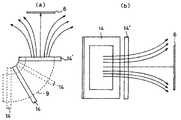
この公報等に記載の従来の真空アーク蒸着装置(アーク式イオンブレーディング装置)は、図9の平面図に示すように形成される。
【0007】
そして、成膜室1を形成する金属製の接地された真空容器2は、図示省略した真空排気装置によって右側の排気口3から排気され、左側のガス導入口4から、アルゴンガス等の不活性ガスや反応性ガスが導入される。
【0008】
また、前記公報においては、成膜室1の円筒形のホルダに基材を複数個取付けた構造が示されているが、図9においては、説明を簡単にするため、成膜室1のほぼ中央に平板状の1個のホルダ5が、その表面を前方に向けて、かつ、回転自在に設けられ、このホルダ5の表面側に基材6が着脱自在に保持される。
【0009】
この基材はホルダ5を介してバイアス電源7の陰極に接続され、基材6が真空容器2に対して代表的には−50V〜−500Vに直流バイアスされる。
【0010】
なお、図中の8はバイアス電源7の陰極を絶縁する真空容器2の後面板2′の絶縁体である。
【0011】
つぎに、真空容器2の前方にほぼ「ノ」の字状に湾曲した断面矩形の金属製のダクト9が設けられ、このダクト9は、前側一端の接地された端板9′の中央部に絶縁体10を介して蒸発源11が設けられ、この蒸発源11に陽極接地の数10V程度のアーク電源12の陰極が接続され、ダクト9が陽極、蒸発源11が陰極を形成する。
【0012】
なお、ダクト9を陽極に兼用する代わりに、ダクト9と別個に陽極電極が設けられることもある。
【0013】
また、蒸発源11は、図示省略した水冷機構、真空シール機構、トリガ機構等も備える。
【0014】
さらに、ダクト9の他端が真空容器2の前面板2″の中央部に取付けられ、ダクト9の他端の放出口13が成膜室1に連通し、このとき、放出口13の左右方向(水平方向)の放出面の中心がホルダ5、基材6の中心に重なる。
【0015】
つぎに、ダクト9の両端間の複数個所それぞれに、ダクト9を囲んだ磁石としての電磁コイル14′,14が設けられる。
【0016】
このとき、従来は、放出口13に最も近い終端磁石としての電磁コイル14′及び他の電磁コイル14が全て同じ大きさ(寸法)に形成される。
【0017】
さらに、各電磁コイル14′,14は電流源としてのコイル電源15の出力両端間に直列接続され、制御装置16のコイル電流の制御により、各電磁コイル14′,14の通電が制御され、この制御に基づく各電磁コイル14′,14の通電により、図中の実線矢印のループに示すダクト9に沿って湾曲した偏向磁場17が形成され、この磁場17が磁気フィルタ18を形成する。
【0018】
そして、陽極であるダクト9と陰極である蒸発源11との間の真空アーク放電により、蒸発源11のTi,Cr,Mo,Ta,W,Al,Cuのような単体金属、TiAlのような合金等の導電体の陰極材料19が蒸発する。
【0019】
さらに、アーク放電によって生成された電子及び陰極材料19のイオンを含んだ破線矢印のプラズマ流20が偏向磁場17に沿ってダクト9の一端から他端の放出口13に輸送される。
【0020】
このとき、蒸発源11から飛出したドロップレットは、電気的に中性であるか、又は、プラズマ中で負に帯電したりするが、いずれにしても質量が非常に大きいため、偏向磁場17に関係なく直進し、ダクト9の内壁に衝突して除去される。
【0021】
そして、放出口13に到達した陰極材料19のイオンは、バイアス電源7による基材6の大きな負電位のバイアスに基づき、成膜室1に引出されて基材6の表面に飛着し、基材6の表面に陰極材料19の蒸着膜が成膜される。
【0022】
なお、陰極材料19のイオンの引出しに連動してガス導入口4から成膜室1内に反応性ガスを導入すると、このガスが陰極材料19のイオンと反応し、基材6の表面に、例えば炭化チタンや窒化チタン等の金属化合物薄膜が蒸着される。
【0023】
【発明が解決しようとする課題】
前記図9の従来装置の真空アーク蒸着においては、終端磁石の電磁コイル14′が放出口13の放出面及び基材6に平行に設置される。
【0024】
一方、一様な磁場中で電子が輸送される状態を考えると、よく知られるように、電子はつぎの数1の式のローレンツ力Fを受ける。
【0025】
【数1】
F=v×B(v:電子の速度ベクトル、B:磁束密度のベクトル、×はベクトル積(外積)演算子)
【0026】
そして、このローレンツ力Fにより、電子が螺旋状に回転しながら偏向磁場17の磁力線に沿って進む。
【0027】
そして、陰極材料19のイオンは、この電子に引張られるようにダクト9内を進んで放出口13に輸送される。
【0028】
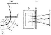
ところで、終端磁石の電磁コイル14′の付近では図10の(a),(b)の実線矢印の磁力線に示すように発散磁場になり、放出口13に到達した電子はこの発散磁場に沿って飛行する。
【0029】
なお、図10の(a),(b)は図9の4個の電磁コイル14,14′のうちの1つおきの2個の電磁コイル14,14′のみ通電した場合の磁力線を示す平面図,右側面図である。
【0030】
この磁力線に沿う電子の飛行軌跡は、電子に引っ張られて移動する陰極材料19のイオンの飛行軌跡に相当し、電子の飛行軌跡から陰極材料19のイオンの軌跡を把握できる。
【0031】
そして、図10の(a),(b)の磁力線に基づく電子の飛行軌跡は、図11の(a),(b)の平面図,右側面図の実線に示すようになる。
【0032】
すなわち、前記の発散磁場により、電子の基材到達位置が、湾曲の向きに応じて、基材6の中心から左方向に大きく偏向し、上下方向(垂直方向)には大きく発散する。
【0033】
また、発散磁場をBとすると、この磁場Bの勾配∇Bが発生し、電子のような荷電粒子は、つぎの数2の式に示す速度VBで勾配∇Bが磁場Bに重なるように回転したときに右ねじが進む方向にドリフトし、この∇Bドリフトによって電子の軌跡が一層ずれる。
【0034】
【数2】
VB=−μ・(∇B×B)/(q・B2),(μ:透磁率、q:電荷、B:磁場ベクトル、∇B:磁場Bの勾配ベクトル、×はベクトル外積の演算子、・はベクトル内積の演算子)
【0035】
したがって、陰極材料19のイオンを、基材6表面中心等の所望の位置を中心にして飛着させることができない。
【0036】
なお、ダクト9及び電磁コイル14,14′が断面矩形の場合、矩形の電磁コイル14,14′の磁場特性に基づき、中心部よりも外寄りになる程、磁場の勾配∇Bが強くなるため、斜め下方向のドリフト速度が大きくなり、陰極材料19の飛着位置の上方向の発散より、下方向の発散が大きくなる。
【0037】
そして、陰極材料19のイオンの飛着中心を、例えば基材6表面の中心部に制御することができないため、電磁コイル14,14′を通流するコイル電流の向きを周期的に逆に切換えて陰極材料19のイオンの飛着位置を周期的にずらすようにしても、基材6に陰極材料19を、所望の位置へ薄膜を蒸着して成膜することができず、均一な成膜特性を得るには十分とはいえない問題点がある。
【0038】
本発明は、終端磁石(電磁コイル14′)の付近での発散磁場に基づく陰極材料19の蒸着位置の左右方向のずれや上下方向の発散を防止し、基材6に均一な蒸着薄膜を成膜し得るようにすることを課題とし、さらには、陰極材料19のイオンの基材到達位置を自由に制御して成膜特性の一層の向上等を図ることも課題とする。
【0039】
【課題を解決するための手段】
前記の課題を解決するために、本発明の請求項1の真空アーク蒸着方法は、放出口に最も近い終端磁石を、放出口の放出面に対し傾けて設置し、終端磁石の発生磁場により、陰極材料のイオンの飛着方向を制御する。
【0040】
したがって、終端磁石により生じる磁場が、従来のように終端磁石を放出面に平行に設置する場合と異なり、終端磁石を放出面に対して適当な角度傾けて設置することにより、陰極材料のイオンが基材表面の中心部に飛着するようになる。
【0041】
また、終端磁石の設置角度を種々に定めることにより、陰極材料のイオンが基材表面の所望位置に飛着するようになり、所望の成膜特性で蒸着膜を成膜することができる。
さらに、各磁石を形成する電磁コイルのコイル電流の向きを一定時間毎に切換えて逆にするため、電子のドリフト方向を逆転することによって陰極材料のイオンの飛着位置を周期的にずらすことができ、大面積の基材の均一蒸着等が可能になる。
【0042】
つぎに、本発明の請求項2の真空アーク蒸着方法の場合は、終端磁石の設置角度を可変自在にする。
【0043】
したがって、終端磁石の設置角度を成膜前及び成膜中に自在に変えることができ、種々の成膜特性の蒸着薄膜を自在に成膜することができる。
【0044】
つぎに、本発明の請求項3の真空アーク蒸着方法の場合、終端磁石が他の磁石と異なる大きさにする。
【0045】
したがって、終端磁石の発散磁場につき、とくに、その上下方向の発散を、終端磁石の大きさを変えることで、種々に制御することができ、例えば、終端磁石を他の磁石より大きくすれば、放出口より基材側での磁場の上下方向の発散を良好に抑制し、陰極材料の蒸着粒子(イオン)の上下方向の拡がりを防止することができ、請求項1,2の成膜特性より一層良好な特性で均一な成膜が行える。
【0046】
そして、請求項1,2,3の真空アーク蒸着方法において、終端磁石の設置角度が自動制御されることが好ましい。
【0047】
さらに、終端磁石の設置角度の制御に連動して各磁石の電磁コイルのコイル電流を制御することが、成膜特性上からは一層好ましい。
【0048】
つぎに、蒸発源を複数個にすれば、成膜能力の向上が図れ、複数種類の陰極材料の同時成膜も行える。
【0050】
つぎに、本発明の請求項7の真空アーク蒸着装置は、放出口に最も近い終端磁石を、放出口の放出面に対し傾けて設置し、かつ、各磁石が電磁コイルからなり、各電磁コイルのコイル電流の向きを一定時間毎に切換えて逆にし、終端磁石の発生磁場により、イオンの飛着方向を制御したものである。
【0051】
また、本発明の請求項8の真空アーク蒸着装置は、終端磁石の設置角度を可変する手段を備えたものである。
【0052】
したがって、請求項1,2の蒸着方法に用いられる真空アーク蒸着装置を提供することができる。
【0053】
さらに、請求項9の真空アーク蒸着装置は、終端磁石が他の磁石と異なる大きさにしたものである。
【0054】
したがって、請求項7,8の蒸着装置に、上下方向の磁場発散抑制機能等を付加することができる。
【0055】
そして、請求項7,8,9の蒸着装置において、終端磁石の設置角度の自動制御手段を備えることが望ましい。
【0056】
また、終端磁石の設置角度の制御に連動して各磁石の電磁コイルのコイル電流を制御する手段を備えることが、成膜特性を向上する上からは、一層好ましい。
【0057】
さらに、蒸発源が複数個であってもよい。
【0058】
【発明の実施の形態】
本発明の実施の1形態につき、図1ないし図8を参照して説明する。
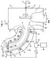
図1は図9に対応する真空アーク蒸着装置の平面図であり、図と同一記号は同一のものを示す。
【0059】
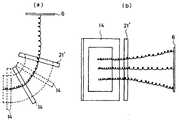
そして、図1においては、図9の終端磁石としての電磁コイル14′の代わりに、他の電磁コイル14より大きい電磁コイル21を、終端磁石として設ける。
【0060】
この電磁コイル21は図2の斜視図に示すように断面矩形の枠状に形成され、図3の(a),(b)のダクト取付状態の平面図,右側面図に示すように、左右方向をX軸方向(左方が正),前後方向をY軸方向(後方が正),上下方向をZ軸方向(上方が正)とすると、放出口13の放出面に平行な破線の状態から、X−Y軸の平面内で角度α,Y−Z軸の平面内で角度β傾けて設置される。
【0061】
この角度α,βは事前の荷電粒子軌道解析シミュレーション及び試験蒸着等に基づいて最適に定められ、この形態にあっては、作業員の手作業で電磁コイル21のダクト9への取付け角度等を調整し、電磁コイル21を放出面に対して角度α,βのいずれか一方又は両方傾ける。
【0062】
そして、この角度α,βの傾きにより、電磁コイル21の発生磁場が制御され、放出口13付近で図9の磁場17と異なる偏向磁場17′の磁気フィルタ22が形成され、この磁気フィルタ22によって図9のプラズマ電流20に相当するプラズマ流23が生成される。
【0063】
このとき、図4の(a),(b)の電子軌跡の平面図,右側面図に示すように、ダクト9を通って基材6の表面に到達する電子の軌跡は、電子の基材到達位置の中心がほぼ基材6表面の中心に一致するように補正される。
【0064】
なお、図4の(a),(b)は電磁コイル21の設置角度による効果を示すため、電磁コイル21の代わりに、他の電磁コイル14と同じ大きさの電磁コイル21′を設け、その設置角度αを時計方向の15度にして左右方向の磁場の発散を収束補正した場合の電子軌跡を示したものであり、図11の(a),(b)と同様、実線の1つおきの2個の電磁コイル21′,14にのみ通電している。
【0065】
つぎに、電磁コイル21は他の電磁コイル14と大きさが異なり、この形態にあっては上下方向の磁場の発散を抑えるため、他の電磁コイル14より大型である。
【0066】
そして、電磁コイル21を他の電磁コイル14より大型にすると、上下方向の磁場に対する磁場フォーカシングの機能が付加され、上下方向の磁場が収束補正され、例えば、図5の(a),(b)の電子軌跡の平面図,右側面図に示すように、電子の上下方向の軌跡が基材6表面の中央寄りに補正されることが実験によって確められた。
【0067】
なお、図5の(a),(b)は、電磁コイル21の設置角度αを時計方向の15度にし、かつ、その寸法を他の電磁コイル14の120%にした場合の電子軌跡であり、図4の(a),(b)の場合と同様、実線の1つおきの2個の電磁コイル21,14にのみ通電している。
【0068】
そして、図4,図5からも明かなように、電子軌跡が基材6の表面付近で左右方向及び上下方向とも中央寄りに補正されるため、陰極材料19のイオンも、左右方向及び上下方向の飛着のずれ,拡散が中央寄りに補正されて防止され、この結果、基材6の表面に均一な成膜が行える。
【0069】
つぎに、具体的な実験結果について説明する。
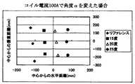
まず、放出口13の放出面と基材6とを、中心が重合し、かつ、両者の距離が400mmになるようにセットし、電磁コイル21,14のコイル電流100Aの条件下、電磁コイル21の設置角度αを時計方向の15度,20度,25度にしたところ、電子軌跡の基材6表面の到達位置の左右方向(水平方向),上下方向(垂直方向)の基材6表面の中心からのずれは図6に示すようになった。
【0070】
図6において、◆は設置角度αが0度のリファレンス(基準コイル)のプロットを示し、■,△,●は設置角度αを15度,20度,25度傾けたときのプロットである。
【0071】
また、設置角度αを15度にしてコイル電流を30A,50A,100Aにすると、電子軌跡のずれは図7に示すようになった。
【0072】
図7において、◆は設置角度αが0度でコイル電流が50Aのリファレンスのプロット、■,△,●は設置角度αが15度でコイル電流が30A,50A,100Aのときのプロットである。
【0073】
そして、図6,図7からも明らかなように、設置角度αをコイル電流に応じて適当に設定し、電磁コイル21を放出口13の放出面に対して適当に傾けると、その影響により、基材6表面でのとくに左右方向の電子到達位置が基材6の中央寄りに補正され、陰極材料19が基材6の表面中央部を中心として蒸着する。
【0074】
つぎに、設置角度αを15度とし、コイル電流30A,50A,100Aの条件下、電磁コイル21の大きさを80%,100%,120%にすると、図8の(a),(b),(c)の結果が得られた。
【0075】
図8の(a),(b),(c)において、◆は設置角度αが0度で100%の大きさのリファレンスのプロット、■,△,●は設置角度αが15度で80%,100%,120%の大きさにした場合のプロットを示す。
【0076】
また、図8の(b)の▲は、△の場合と同様、設置角度15度で100%の大きさにし、かつ、コイル電流の向きを他のプロットと逆にした場合のプロットを示す。
【0077】
そして、図8の(a),(b),(c)からも明らかなように、電磁コイル21を120%に大きくすれば、磁場の発散の抑制により、基材6表面での上下方向の電子到達位置も基材6の中央寄りに補正され、陰極材料19が基材6表面の中央部を中心として、一層良好に蒸着し、均一な成膜が行われる。
【0078】
すなわち、この形態の場合、終端磁石としての電磁コイル21を、放出口13の放出面に対して角度α,βのいずれか一方又は両方傾けて設置し、かつ、電磁コイル21を他の電磁コイル14より大きくしたため、陰極材料19のイオンの飛着方向を、左右方向,上下方向に制御して中央寄りに補正し、陰極材料19を、基材6表面の中央部を中心に飛着させて蒸着し、基材6表面に均一な蒸着薄膜を成膜することができる。
【0079】
ところで、前記形態では陰極材料19を基材6表面の中央部を中心に飛着させて蒸着するように補正したが、基材6によってはその表面中央部から離れた位置を中心に蒸着することが好ましい場合もある。
【0080】
このような場合は、前記の角度α,βの一方又は両方を目的に応じて設定し、基材6表面の任意の位置を中心に蒸着するようにしてもよい。
【0081】
つぎに、前記形態では作業員の手作業で電磁コイル21を角度α,βだけ事前に傾けたが、例えば、電磁コイル21をX−X軸の平面内で回動してその角度αを可変する治具と、電磁コイル21をZ−Y軸の平面内で回動してその角度βを可変する治具とのいずれか一方又は両方を、電磁コイル21の設置角度を自在に可変する手段として設け、事前の試験成膜の結果に基づいて電磁コイル21の設置角度を初期設定したり、実際の蒸着中に電磁コイル21の設置角度を可変するようにしてもよい。
【0082】
また、前記形態では終端磁石及び他の磁石をいずれも電磁コイル21,14としたが、これらの磁石はいわゆる永久磁石で形成してもよい。
【0083】
さらに、前記形態では、説明を簡単にするため、蒸発源11が1個の場合について説明したが、基材6が大面積の場合や複数種類の陰極材料を同時に蒸着する場合等には、蒸発源11を、例えば上下方向に複数個設ければよい。
【0084】
つぎに、終端磁石の設置角度は、例えば図9の制御装置16の代わりに設けた図1の制御装置24のシーケンス制御,プログラム制御等が形成する自動制御手段により、図示省略した膜厚計による基材6表面の膜厚の計測に基づき、事前に又は実際の成膜の進行に応じて前記の両治具を自動制御し、この自動制御によって自動設定したり成膜中に自動可変することが、実用的であり、また、成膜作業の効率化等の面からも、好ましい。
【0085】
さらに、各磁石が電磁コイル14,21からなる場合、制御装置24の通電制御手段により、前記の膜厚計の計測に基づき、成膜中の電磁コイル21の設置角度α,βの制御に連動して各電磁コイル14,21のコイル電流を制御すれば、一層精度の高い成膜が行える。
【0086】
その上、制御装置24の通電制御手段により、各電磁コイル14,21のコイル電流の向きを一定時間毎に切換えて逆にすることにより、電流方向の逆転により、磁場Bの勾配∇Bの方向は変化しないが、磁場Bの方向が反転して変化するため、プラズマ流23の輸送に作用するドリフト速度が変わり、基材6の表面への陰極材料19の飛着方向が変化して膜厚分布の一層の均一化を図ることができ、成膜特性が一層向上する。
【0087】
また、各電磁コイル21,14のコイル電流を交流電源から得るようにすれば、前記の通電制御手段による切換えを行うことなく、各電磁コイル21,14の電流方向を一定時間毎に逆転することができる。
【0089】
また、前記形態においては、1個のダクト9を真空容器2に接続して真空アーク蒸着装置を形成したが、真空容器2に複数のダクトを接続し、各ダクトの終端磁石を、各ダクトの放出口の放出面に対して、それぞれ傾けるようにしてもよい。
【0090】
さらに、前記形態では説明を簡単にするため、成膜室1内に、1個のホルダ5を設け、1個の基材6を蒸着して成膜するようにしたが、例えば、前記公報に記載のアーク式イオンブレーディング装置のように、成膜室内に円筒形の回転式のホルダを設け、このホルダの各面に基材を保持して複数の基材の真空アーク蒸着を行う場合にも、本発明は同様に適用することができる。
【0091】
つぎに、前記形態では電磁コイル21を他の電磁コイル14より大きくして終端磁石を他の磁石より大きくしたが、放出口13と基材6の距離が近いなど成膜条件等によっては、終端磁石を他の磁石より小さくして良好な成膜特性を得ることができる場合もあり、このような場合には、終端磁石を他の磁石より小さくすればよい。
【0092】
また、前記形態では湾曲したダクト9を用いた場合について説明したが、ダクト9の代わりに屈曲したダクトを用いた場合にも、本発明は同様に適用することができる。
【0093】
つぎに、成膜特性の一層の向上等を図る場合は、終端磁場(電磁コイル21)の左右方向及び上下方向のいずれか一方又は両方の設置角度を調整するだけでなく、他の磁石(電磁コイル14)の全部又は一部についても、終端磁石と同様に、左右方向及び上下方向のいずれか一方又は両方の設置角度を調整することが好ましい。
【0094】
【発明の効果】
本発明は、以下に記載する効果を奏する。
まず、請求項1の真空アーク蒸着方法の場合、放出口13に最も近い終端磁石(電磁コイル21)を、放出口13の放出面に対し傾けて設置し、終端磁石の発生磁場により、陰極材料19のイオンの飛着方向を制御したため、終端磁石により生じる偏向磁場が、従来の終端磁石を放出面に平行に設置する場合と異なり、陰極材料19のイオンを基材6表面の中心部に到達するように制御し、均一な蒸着膜の成膜を行うことができる。
【0095】
また、終端磁石の設置角度を種々に定めることにより、陰極材料19のイオンが基材表面の所望の位置を中心にして飛着するようになり、所望の成膜特性で蒸着膜を成膜することができる。
さらに、とくに、各磁石を形成する電磁コイルのコイル電流の向きを一定時間毎に切換えて逆にするため、電子のドリフト方向を逆転することによって陰極材料のイオンの飛着位置を周期的にずらすことができ、大面積の基材の均一蒸着等が可能になる。
【0096】
つぎに、請求項2の真空アーク蒸着方法の場合は、終端磁石の設置角度を可変自在にしたため、終端磁石の設置角度を成膜前及び成膜中に自在に変えることができ、種々の成膜特性の蒸着薄膜を自在に成膜することができる。
【0097】
つぎに、請求項3の真空アーク蒸着方法の場合、終端磁石を他の磁石と異なる大きさにしたため、終端磁石の発散磁場につき、とくに、その上下方向の発散を、終端磁石の大きさを変えることで、種々に制御することができ、例えば、終端磁石を他の磁石より大きくして磁場の上下方向の発散を良好に抑制し、請求項1,2の成膜特性より一層均一な特性にすることができる。
また、終端磁石の設置角度が自動制御されることが実用上は好ましい。
【0098】
さらに、終端磁石の設置角度の制御に連動して各磁石の電磁コイル14,21のコイル電流を制御することが、成膜特性上からは一層好ましい。
【0099】
つぎに、蒸発源11を複数個にすれば、成膜能力の向上が図れ、複数種類の陰極材料19の同時成膜も行うことができる。
【0101】
つぎに、請求項7〜12の真空アーク蒸着装置は、前記の各真空アーク蒸着方法を実現する具体的な装置を提供することができる。
【図面の簡単な説明】
【図1】 本発明の実施の1形態の真空アーク蒸着装置の平面図である。
【図2】 図1の終端磁石としての電磁コイルの斜視図である。
【図3】 (a),(b)は図2の電磁コイルの傾きの説明図である。
【図4】 (a),(b)は終端磁石としての電磁コイルを角度α=15度傾けたときの電子軌跡説明図の平面図,右側面図である。
【図5】 (a),(b)は終端磁石としての電磁コイルを角度α=15度傾け、かつ、その寸法を他の磁石の電磁コイルより大きくしたときの電子軌跡説明図の平面図,右側面図である。
【図6】 終端磁石としての電磁コイルの角度αを変えたときの電子到達位置の実測結果である。
【図7】 終端磁石としての電磁コイルを角度α=15度傾けてコイル電流を変えたときの電子到達位置の実測結果である。
【図8】 (a),(b),(c)は終端磁石としての電磁コイルを角度α=15度傾けてコイル電流を30A,50A,100Aにしたときの大きさ(コイル寸法)の違いによる電子到達位置の実測結果である。
【図9】 従来装置の平面図である。
【図10】 (a),(b)は図9の従来装置の発散磁場説明図の平面図,右側面図である。
【図11】(a),(b)は図9の従来装置の電子軌跡説明図の平面図,右側面図である。
【符号の説明】
1 成膜室
6 基材
9 ダクト
11 蒸発源
13 放出口
14,21 電磁コイル
17′ 偏向磁場
19 陰極材料
22 磁気フィルタ
23 プラズマ流[0001]
BACKGROUND OF THE INVENTION
The present invention relates to a vacuum arc evaporation method and apparatus for forming a thin film on a surface of a base material in order to improve the wear resistance of the base material such as an automobile part, a machine part, a tool, and a mold.
[0002]
[Prior art]
In general, vacuum arc deposition is a simple thin film forming method in which arc discharge is generated between a cathode and an anode, and the cathode material is evaporated and deposited on a base material, and is characterized by excellent productivity.
[0003]
However, from the cathode material (also from the cathode depending on the discharge state), large, coarse particles (droplets) having a diameter of several μm are ejected, and the droplets adhere to the substrate, resulting in poor film formation characteristics. It is known to
[0004]
In order to prevent deterioration of the film formation characteristics due to this droplet, a magnet such as an electromagnetic coil is used.TheA magnetic field is generated between the cathode and the substrate, droplets are removed by this magnetic field, and the deposition method transports only the plasma flow in the direction of the substrate along the magnetic field. A vapor deposition method has been proposed in which the droplets are dissolved by forming them.
[0005]
A conventional vacuum arc deposition method and apparatus for transporting only the former plasma flow in the direction of the substrate is described in Japanese Patent Application Laid-Open No. 2001-59165 (
[0006]
The conventional vacuum arc vapor deposition apparatus (arc type ion braiding apparatus) described in this publication is formed as shown in the plan view of FIG.
[0007]
The metal grounded
[0008]
In the above publication, a structure in which a plurality of substrates are attached to a cylindrical holder of the film forming chamber 1 is shown. However, in FIG. A flat plate-
[0009]
This base material is connected to the cathode of the bias power source 7 through the
[0010]
In the figure,
[0011]
Next, a
[0012]
Note that an anode electrode may be provided separately from the
[0013]
The
[0014]
Further, the other end of the
[0015]
Next,
[0016]
At this time, conventionally, the
[0017]
Further, the
[0018]
Then, by vacuum arc discharge between the
[0019]
Further, a plasma flow 20 indicated by a broken arrow including electrons generated by arc discharge and ions of the cathode material 19 is transported along the deflection
[0020]
At this time, the droplets ejected from the
[0021]
Then, the ions of the cathode material 19 that have reached the
[0022]
When a reactive gas is introduced into the film forming chamber 1 from the gas inlet 4 in conjunction with the extraction of the ions of the cathode material 19, this gas reacts with the ions of the cathode material 19, and on the surface of the
[0023]
[Problems to be solved by the invention]
In the vacuum arc deposition of the conventional apparatus shown in FIG. 9, the
[0024]
On the other hand, considering the state in which electrons are transported in a uniform magnetic field, as is well known, the electrons receive a Lorentz force F of the following equation (1).
[0025]
[Expression 1]
F = v × B (v: electron velocity vector, B: magnetic flux density vector, x is a vector product (outer product) operator)
[0026]
And by this Lorentz force F, an electron advances along the magnetic force line of the deflection
[0027]
The ions of the cathode material 19 travel through the
[0028]
By the way, in the vicinity of the
[0029]
10 (a) and 10 (b) are planes showing lines of magnetic force when only every other two
[0030]
The flight trajectory of the electrons along the magnetic field lines corresponds to the flight trajectory of the cathode material 19 moving by being pulled by the electrons, and the trajectory of the ions of the cathode material 19 can be grasped from the electron flight trajectory.
[0031]
Then, the flight trajectory of electrons based on the magnetic lines of force in FIGS. 10A and 10B is as shown by the solid lines in the plan view and right side view of FIGS. 11A and 11B.
[0032]
That is, due to the divergent magnetic field, the base material arrival position of electrons is greatly deflected to the left from the center of the
[0033]
Further, if the divergent magnetic field is B, a gradient ∇B of the magnetic field B is generated, and charged particles such as electrons have a velocity V shown in the following equation (2).BWhen the gradient ∇B rotates so as to overlap the magnetic field B, the right-hand screw drifts in the traveling direction, and this ∇B drift further shifts the electron trajectory.
[0034]
[Expression 2]
VB = −μ · (∇B × B) / (q · B2), (μ: permeability, q: charge, B: magnetic field vector, ∇B: gradient vector of magnetic field B, x is an operator of vector cross product,・ Is a vector dot product operator)
[0035]
Therefore, the ions of the cathode material 19 cannot be made to strike around a desired position such as the center of the surface of the
[0036]
Note that when the
[0037]
Since the ion landing center of the cathode material 19 cannot be controlled, for example, at the center of the surface of the
[0038]
The present invention prevents the horizontal displacement and vertical divergence of the deposition position of the cathode material 19 based on the divergent magnetic field in the vicinity of the terminal magnet (electromagnetic coil 14 '), and forms a uniform vapor deposition thin film on the
[0039]
[Means for Solving the Problems]
In order to solve the above-mentioned problem, the vacuum arc vapor deposition method according to claim 1 of the present invention is configured such that the terminal magnet closest to the discharge port is inclined with respect to the discharge surface of the discharge port, and the magnetic field generated by the terminal magnet is Controls the ion landing direction of the cathode material.
[0040]
Therefore, the magnetic field generated by the terminal magnet is different from the case where the terminal magnet is installed parallel to the emission surface as in the prior art. It will come to the center of the substrate surface.
[0041]
In addition, by setting the installation angle of the terminal magnets in various ways, the ions of the cathode material come to land at a desired position on the surface of the substrate, and a deposited film can be formed with desired film formation characteristics.
Furthermore, in order to reverse the direction of the coil current of the electromagnetic coil forming each magnet at regular intervals, it is possible to periodically shift the ion landing position of the cathode material by reversing the electron drift direction. It is possible to uniformly deposit a large area substrate.
[0042]
Next, in the vacuum arc deposition method according to
[0043]
Accordingly, the installation angle of the terminal magnet can be freely changed before and during film formation, and vapor deposition thin films having various film formation characteristics can be formed freely.
[0044]
Next, in the vacuum arc vapor deposition method according to
[0045]
Therefore, the divergence magnetic field of the terminal magnet can be controlled in various ways by changing the size of the terminal magnet, particularly the vertical divergence. For example, if the terminal magnet is made larger than the other magnets, The divergence in the vertical direction of the magnetic field on the substrate side from the outlet can be satisfactorily suppressed, and the vertical spread of the vapor deposition particles (ions) of the cathode material can be prevented. Uniform film formation can be performed with good characteristics.
[0046]
And in the vacuum arc vapor deposition method of
[0047]
furtherThe endFrom the viewpoint of film forming characteristics, it is more preferable to control the coil current of the electromagnetic coil of each magnet in conjunction with the control of the installation angle of the end magnet.
[0048]
Next, if a plurality of evaporation sources are used, the film forming capability can be improved, and a plurality of types of cathode materials can be simultaneously formed.
[0050]
Next, the claims of the present invention7The vacuum arc vapor deposition equipment of this type is installed with the terminal magnet closest to the discharge port inclined to the discharge surface of the discharge port.And each magnet consists of an electromagnetic coil, the direction of the coil current of each electromagnetic coil is switched every predetermined time and reversed, and the ion landing direction is controlled by the magnetic field generated by the terminal magnet.It is a thing.
[0051]
Further, the claims of the present invention8The vacuum arc vapor deposition apparatus includes a means for changing the installation angle of the terminal magnet.
[0052]
Therefore, the vacuum arc vapor deposition apparatus used for the vapor deposition method of
[0053]
And claims9In the vacuum arc deposition apparatus, the size of the terminal magnet is different from that of other magnets.
[0054]
Therefore, the claims7,8In addition, a vertical magnetic field divergence suppressing function and the like can be added to the vapor deposition apparatus.
[0055]
And claims7,8,9In the vapor deposition equipmentThe endIt is desirable to provide automatic control means for the end magnet installation angle.
[0056]
AlsoThe endIn order to improve the film forming characteristics, it is more preferable to provide means for controlling the coil current of the electromagnetic coil of each magnet in conjunction with the control of the installation angle of the end magnet.
[0057]
In addition, there may be multiple evaporation sources.Yes.
[0058]
DETAILED DESCRIPTION OF THE INVENTION
An embodiment of the present invention will be described with reference to FIGS.
FIG. 1 is a plan view of a vacuum arc vapor deposition apparatus corresponding to FIG. 9, and the same symbols as those in FIG.
[0059]
In FIG. 1, an
[0060]
As shown in the perspective view of FIG.cross sectionAs shown in the plan view and right side view of the duct mounted state in FIGS. 3A and 3B, the left and right direction is the X-axis direction (left is positive), and the front and rear direction is Assuming that the Y-axis direction (backward is positive) and the up-down direction is Z-axis direction (upward is positive), the angle α, Y− Installed at an angle β in the plane of the Z axis.
[0061]
The angles α and β are optimally determined based on the charged particle trajectory analysis simulation and test vapor deposition in advance. In this embodiment, the mounting angle of the
[0062]
The magnetic field generated by the
[0063]
At this time, as shown in the plan view and right side view of the electron trajectory in FIGS. 4A and 4B, the trajectory of the electrons passing through the
[0064]
4A and 4B show the effect of the installation angle of the
[0065]
Next, the
[0066]
When the
[0067]
5A and 5B are electron trajectories when the installation angle α of the
[0068]
4 and 5, since the electron trajectory is corrected near the center in the left-right direction and the up-down direction near the surface of the
[0069]
Next, specific experimental results will be described.
First, the discharge surface of the
[0070]
In FIG. 6, ♦ indicates a plot of a reference (reference coil) having an installation angle α of 0 degrees, and ▪, Δ, and ● indicate plots when the installation angle α is inclined by 15 degrees, 20 degrees, and 25 degrees.
[0071]
Further, when the installation angle α is set to 15 degrees and the coil current is set to 30A, 50A, and 100A, the deviation of the electron trajectory is as shown in FIG.
[0072]
In FIG. 7, ♦ is a reference plot when the installation angle α is 0 degree and the coil current is 50 A, and ■, Δ, and ● are plots when the installation angle α is 15 degrees and the coil current is 30 A, 50 A, and 100 A.
[0073]
As apparent from FIGS. 6 and 7, when the installation angle α is appropriately set according to the coil current and the
[0074]
Next, assuming that the installation angle α is 15 degrees and the size of the
[0075]
In FIGS. 8A, 8B, and 8C, ♦ is a reference plot with an installation angle α of 0 degrees and 100%, and ■, Δ, and ● are 80% when the installation angle α is 15 degrees. , 100% and 120% are plotted.
[0076]
Also, ▲ in FIG. 8B shows a plot when the installation angle is 15 degrees and the magnitude is 100% and the direction of the coil current is reversed from the other plots, as in the case of △.
[0077]
As is clear from FIGS. 8A, 8B, and 8C, if the
[0078]
That is, in the case of this embodiment, the
[0079]
By the way, in the said form, although it correct | amended so that the cathode material 19 might be deposited and deposited centering on the center part of the base-
[0080]
In such a case, one or both of the angles α and β may be set according to the purpose, and vapor deposition may be performed with an arbitrary position on the surface of the
[0081]
Next, in the above embodiment, the
[0082]
Moreover, although the terminal magnet and the other magnet are both
[0083]
Further, in the above embodiment, the case where the number of
[0084]
Next, the installation angle of the terminal magnet is determined by an automatic control means formed by sequence control, program control, etc. of the
[0085]
Further, when each magnet is composed of the
[0086]
MoreoverThe direction of the coil current of each of the
[0087]
Further, if the coil currents of the
[0089]
Moreover, in the said form, although the one
[0090]
Furthermore, in order to simplify the explanation in the above embodiment, one
[0091]
Next, in the above embodiment, the
[0092]
Moreover, although the case where the
[0093]
Next, when further improving the film formation characteristics, etc., not only the installation angle of one or both of the left and right directions and the vertical direction of the terminal magnetic field (electromagnetic coil 21) is adjusted, but other magnets (electromagnetic For all or part of the coil 14), it is preferable to adjust the installation angle in one or both of the left-right direction and the up-down direction, similarly to the terminal magnet.
[0094]
【The invention's effect】
The present invention has the following effects.
First, in the vacuum arc vapor deposition method according to claim 1, the terminal magnet (electromagnetic coil 21) closest to the
[0095]
In addition, by determining the installation angle of the terminal magnet in various ways, the ions of the cathode material 19 come to scatter around the desired position on the surface of the base material, and a deposited film is formed with desired film formation characteristics. be able to.
Furthermore, in particular, in order to reverse the direction of the coil current of the electromagnetic coil forming each magnet at regular intervals, the ion landing position of the cathode material is periodically shifted by reversing the electron drift direction. And uniform vapor deposition of a large-area substrate becomes possible.
[0096]
Next, in the vacuum arc vapor deposition method according to the second aspect, since the installation angle of the terminal magnet is made variable, the installation angle of the terminal magnet can be freely changed before and during film formation. A vapor-deposited thin film having film characteristics can be freely formed.
[0097]
Next, in the case of the vacuum arc deposition method according to
MaIn addition, it is practically preferable that the installation angle of the terminal magnet is automatically controlled.
[0098]
furtherThe endFrom the viewpoint of film forming characteristics, it is more preferable to control the coil current of the
[0099]
Next, if a plurality of
[0101]
Next, the claim7-12The vacuum arc vapor deposition apparatus can provide a specific apparatus for realizing each of the vacuum arc vapor deposition methods.
[Brief description of the drawings]
FIG. 1 is a plan view of a vacuum arc deposition apparatus according to an embodiment of the present invention.
2 is a perspective view of an electromagnetic coil as a terminal magnet in FIG. 1. FIG.
3A and 3B are explanatory views of the inclination of the electromagnetic coil in FIG.
FIGS. 4A and 4B are a plan view and a right side view of an electron trajectory explanatory diagram when an electromagnetic coil as a terminal magnet is tilted at an angle α = 15 degrees.
FIGS. 5A and 5B are plan views of explanatory diagrams of electron trajectories when the electromagnetic coil as a terminal magnet is inclined at an angle α = 15 degrees and the size thereof is made larger than that of the electromagnetic coil of another magnet; It is a right view.
FIG. 6 is an actual measurement result of the electron arrival position when the angle α of the electromagnetic coil as the terminal magnet is changed.
FIG. 7 is an actual measurement result of an electron arrival position when the coil current is changed by tilting an electromagnetic coil as a terminal magnet by an angle α = 15 degrees.
8 (a), (b), and (c) are differences in size (coil dimensions) when an electromagnetic coil as a terminal magnet is tilted at an angle α = 15 degrees and the coil current is set to 30A, 50A, and 100A. It is the measurement result of the electron arrival position by.
FIG. 9 is a plan view of a conventional device.
FIGS. 10A and 10B are a plan view and a right side view of a divergent magnetic field explanatory diagram of the conventional apparatus of FIG.
FIG. 11(A), (b)It is the top view of the electronic locus explanatory drawing of the conventional apparatus of FIG. 9, and the right view.
[Explanation of symbols]
1 Deposition chamber
6 Base material
9 Duct
11 Evaporation source
13 Release port
14,21 Electromagnetic coil
17 'deflection magnetic field
19 Cathode material
22 Magnetic filter
23 Plasma flow
Claims (12)
Translated fromJapanese前記ダクトの複数個所それぞれに前記ダクトを囲んだ断面矩形の磁石を設けて磁気フィルタを形成し、
前記磁気フィルタにより前記ダクトの内部に偏向磁場を発生し、
前記偏向磁場に基づき、前記蒸発によって発生した粗大粒子を除去しつつ、前記陰極材料のイオンを含むプラズマ流を前記ダクトの一端から他端の放出口に輸送し、
前記プラズマ流の前記イオンを前記放出口から成膜室に引出して前記成膜室の基材に飛着し、
前記基材に前記陰極材料を蒸着する真空アーク蒸着方法において、
前記放出口に最も近い終端磁石を、前記放出口の放出面に対して傾けて設置し、
かつ、前記各磁石が電磁コイルからなり、前記各電磁コイルのコイル電流の向きを一定時間毎に切換えて逆にし、
前記終端磁石の発生磁場により、前記イオンの飛着方向を制御することを特徴とする真空アーク蒸着方法。The cathode material is evaporated by arc discharge from an evaporation source located at one end of a curved or bentrectangular duct.
A magnetic filter is formed by providing arectangular magnet that surrounds the duct at each of a plurality of locations of the duct,
The magnetic filter generates a deflection magnetic field inside the duct,
Based on the deflection magnetic field, while removing the coarse particles generated by the evaporation, transport the plasma flow containing the ions of the cathode material from one end of the duct to the other outlet,
The ions of the plasma flow are drawn out from the discharge port to the film forming chamber and land on the substrate of the film forming chamber,
In the vacuum arc deposition method of depositing the cathode material on the substrate,
A terminal magnet closest to the discharge port is installed to be inclined with respect to the discharge surface of the discharge port,
And each said magnet consists of electromagnetic coils, and reverses the direction of the coil current of each said electromagnetic coil for every fixed time,
A vacuum arc vapor deposition method, wherein a direction in which ions are scattered is controlled by a magnetic field generated by the terminal magnet.
湾曲又は屈曲した断面矩形のダクトと、
前記ダクトの一端に位置し、真空中でのアーク放電により陰極材料が蒸発する蒸発源と、
前記成膜室に連通した前記ダクトの他端の放出口と、
前記ダクトの複数個所それぞれに前記ダクトを囲んだ断面矩形の磁石を設けて形成され、前記ダクト内に偏向磁場を発生し、前記蒸発により発生した粗大粒子を除去しつつ、前記陰極材料のイオンを含むプラズマ流を前記ダクトの一端から前記放出口に輸送する磁気フィルタとを備え、
前記プラズマ流の前記イオンを前記放出口から前記成膜室に引出して前記基材に飛着し、前記基材に前記陰極材料を蒸着する真空アーク蒸着装置において、
前記放出口に最も近い終端磁石を、前記放出口の放出面に対し傾けて設置し、
かつ、前記各磁石が電磁コイルからなり、前記各電磁コイルのコイル電流の向きを一定時間毎に切換えて逆にし、
前記終端磁石の発生磁場により、前記イオンの飛着方向を制御することを特徴とする真空アーク蒸着装置。A film forming chamber provided with a substrate;
A curved or bent duct with arectangular cross section ;
An evaporation source located at one end of the duct and evaporating the cathode material by arc discharge in vacuum;
A discharge port at the other end of the duct communicating with the film forming chamber;
Each of the ducts is formed by providinga magnet having arectangular cross-section surrounding the duct, generating a deflection magnetic field in the duct, and removing the coarse particles generated by the evaporation while ionizing the cathode material. A magnetic filter for transporting a plasma flow comprising from one end of the duct to the outlet,
In a vacuum arc deposition apparatus for extracting the ions of the plasma flow from the discharge port to the film formation chamber and landing on the substrate, and depositing the cathode material on the substrate,
A terminal magnet closest to the discharge port is installed to be inclined with respect to the discharge surface of the discharge port,
And each said magnet consists of electromagnetic coils, and reverses the direction of the coil current of each said electromagnetic coil for every fixed time,
The vacuum arc deposition apparatus characterizedby controlling the ion landing direction by a magnetic field generated by the terminal magnet .
Priority Applications (7)
| Application Number | Priority Date | Filing Date | Title |
|---|---|---|---|
| JP2001365606AJP4003448B2 (en) | 2001-11-30 | 2001-11-30 | Vacuum arc deposition method and apparatus |
| US10/305,008US7033462B2 (en) | 2001-11-30 | 2002-11-27 | Vacuum arc vapor deposition process and apparatus |
| DE60212551TDE60212551T2 (en) | 2001-11-30 | 2002-11-29 | Apparatus and method for vacuum coating by means of an arc |
| KR1020020075172AKR100569905B1 (en) | 2001-11-30 | 2002-11-29 | Vacuum arc vapor deposition process and apparatus |
| EP02026683AEP1316986B1 (en) | 2001-11-30 | 2002-11-29 | Vacuum arc vapor deposition process and apparatus |
| TW91134753ATW575672B (en) | 2001-11-30 | 2002-11-29 | Vacuum arc vapor deposition process and apparatus |
| CNB02160651XACN1205353C (en) | 2001-11-30 | 2002-11-30 | Method and device for vacuum arc vapour deposition |
Applications Claiming Priority (1)
| Application Number | Priority Date | Filing Date | Title |
|---|---|---|---|
| JP2001365606AJP4003448B2 (en) | 2001-11-30 | 2001-11-30 | Vacuum arc deposition method and apparatus |
Publications (2)
| Publication Number | Publication Date |
|---|---|
| JP2003166050A JP2003166050A (en) | 2003-06-13 |
| JP4003448B2true JP4003448B2 (en) | 2007-11-07 |
Family
ID=19175605
Family Applications (1)
| Application Number | Title | Priority Date | Filing Date |
|---|---|---|---|
| JP2001365606AExpired - Fee RelatedJP4003448B2 (en) | 2001-11-30 | 2001-11-30 | Vacuum arc deposition method and apparatus |
Country Status (1)
| Country | Link |
|---|---|
| JP (1) | JP4003448B2 (en) |
Families Citing this family (28)
| Publication number | Priority date | Publication date | Assignee | Title |
|---|---|---|---|---|
| US7033462B2 (en) | 2001-11-30 | 2006-04-25 | Nissin Electric Co., Ltd. | Vacuum arc vapor deposition process and apparatus |
| US7811172B2 (en) | 2005-10-21 | 2010-10-12 | Cfph, Llc | System and method for wireless lottery |
| US8092303B2 (en) | 2004-02-25 | 2012-01-10 | Cfph, Llc | System and method for convenience gaming |
| US20070060358A1 (en) | 2005-08-10 | 2007-03-15 | Amaitis Lee M | System and method for wireless gaming with location determination |
| US8616967B2 (en) | 2004-02-25 | 2013-12-31 | Cfph, Llc | System and method for convenience gaming |
| US7637810B2 (en) | 2005-08-09 | 2009-12-29 | Cfph, Llc | System and method for wireless gaming system with alerts |
| US7534169B2 (en) | 2005-07-08 | 2009-05-19 | Cfph, Llc | System and method for wireless gaming system with user profiles |
| KR100683174B1 (en) | 2005-06-17 | 2007-02-15 | 삼성전자주식회사 | Plasma Accelerator and Plasma Processing System Having the Same |
| US8070604B2 (en) | 2005-08-09 | 2011-12-06 | Cfph, Llc | System and method for providing wireless gaming as a service application |
| US10510214B2 (en) | 2005-07-08 | 2019-12-17 | Cfph, Llc | System and method for peer-to-peer wireless gaming |
| US7549576B2 (en) | 2006-05-05 | 2009-06-23 | Cfph, L.L.C. | Systems and methods for providing access to wireless gaming devices |
| US7644861B2 (en) | 2006-04-18 | 2010-01-12 | Bgc Partners, Inc. | Systems and methods for providing access to wireless gaming devices |
| US8939359B2 (en) | 2006-05-05 | 2015-01-27 | Cfph, Llc | Game access device with time varying signal |
| US12136314B2 (en) | 2006-05-05 | 2024-11-05 | Cfph, Llc | Game access device with time varying signal |
| US9306952B2 (en) | 2006-10-26 | 2016-04-05 | Cfph, Llc | System and method for wireless gaming with location determination |
| US8292741B2 (en) | 2006-10-26 | 2012-10-23 | Cfph, Llc | Apparatus, processes and articles for facilitating mobile gaming |
| US8510567B2 (en) | 2006-11-14 | 2013-08-13 | Cfph, Llc | Conditional biometric access in a gaming environment |
| US8645709B2 (en) | 2006-11-14 | 2014-02-04 | Cfph, Llc | Biometric access data encryption |
| US9411944B2 (en) | 2006-11-15 | 2016-08-09 | Cfph, Llc | Biometric access sensitivity |
| US8581721B2 (en) | 2007-03-08 | 2013-11-12 | Cfph, Llc | Game access device with privileges |
| US8319601B2 (en) | 2007-03-14 | 2012-11-27 | Cfph, Llc | Game account access device |
| US9183693B2 (en) | 2007-03-08 | 2015-11-10 | Cfph, Llc | Game access device |
| DE102010024543A1 (en) | 2010-06-22 | 2011-12-22 | Merck Patent Gmbh | Method and device for coating a surface |
| US20220296999A1 (en) | 2010-08-13 | 2022-09-22 | Cfph, Llc | Multi-process communication regarding gaming information |
| US8956231B2 (en) | 2010-08-13 | 2015-02-17 | Cfph, Llc | Multi-process communication regarding gaming information |
| JP5968666B2 (en)* | 2012-04-09 | 2016-08-10 | 中外炉工業株式会社 | Plasma generator and vapor deposition apparatus |
| JP7395761B2 (en) | 2020-06-19 | 2023-12-11 | ナノフィルム テクノロジーズ インターナショナル リミテッド | Improved cathodic arc source, its filter, and method for screening macroparticles |
| CN115821218B (en)* | 2022-12-23 | 2024-12-13 | 季华实验室 | Film coating device and film coating method |
- 2001
- 2001-11-30JPJP2001365606Apatent/JP4003448B2/ennot_activeExpired - Fee Related
Also Published As
| Publication number | Publication date |
|---|---|
| JP2003166050A (en) | 2003-06-13 |
Similar Documents
| Publication | Publication Date | Title |
|---|---|---|
| JP4003448B2 (en) | Vacuum arc deposition method and apparatus | |
| EP1316986B1 (en) | Vacuum arc vapor deposition process and apparatus | |
| EP1245694B1 (en) | Vacuum arc vapor deposition apparatus and vacuum arc vapor deposition method | |
| US5114556A (en) | Deposition apparatus and method for enhancing step coverage and planarization on semiconductor wafers | |
| JP3868483B2 (en) | Rectangular vacuum arc plasma source | |
| US5798029A (en) | Target for sputtering equipment | |
| US20090071818A1 (en) | Film deposition apparatus and method of film deposition | |
| WO2015134108A1 (en) | Ion beam sputter deposition assembly, sputtering system, and sputter method of physical vapor deposition | |
| US20090314206A1 (en) | Sheet Plasma Film-Forming Apparatus | |
| KR20130121078A (en) | Arc deposition source having a defined electric field | |
| EP2164091B1 (en) | Method for manufacturing sputter-coated substrates, magnetron source and sputtering chamber with such source | |
| TWI296813B (en) | Improvements in and relating to magnetron sputtering | |
| JPH0122729B2 (en) | ||
| JPH02194167A (en) | Vacuum arc evaporation device | |
| US9624570B2 (en) | Compact, filtered ion source | |
| US7022209B2 (en) | PVD method and PVD apparatus | |
| JP2021528815A (en) | Single beam plasma source | |
| JP3744467B2 (en) | Vacuum arc deposition method and apparatus | |
| KR20010021341A (en) | Arc type ion plating apparatus | |
| CN108342701A (en) | Apparatus and methods for surface treatment | |
| JP4339562B2 (en) | Ion plating method and apparatus therefor | |
| JP2022515745A (en) | Magnet configuration for plasma source to perform plasma processing | |
| JPH07138743A (en) | Ion plating device | |
| JP2004010920A (en) | Vacuum arc vapor deposition apparatus | |
| JPH03138363A (en) | Plasma beam sputtering device |
Legal Events
| Date | Code | Title | Description |
|---|---|---|---|
| A621 | Written request for application examination | Free format text:JAPANESE INTERMEDIATE CODE: A621 Effective date:20040421 | |
| A977 | Report on retrieval | Free format text:JAPANESE INTERMEDIATE CODE: A971007 Effective date:20061110 | |
| A131 | Notification of reasons for refusal | Free format text:JAPANESE INTERMEDIATE CODE: A131 Effective date:20070508 | |
| A521 | Written amendment | Free format text:JAPANESE INTERMEDIATE CODE: A523 Effective date:20070703 | |
| TRDD | Decision of grant or rejection written | ||
| A01 | Written decision to grant a patent or to grant a registration (utility model) | Free format text:JAPANESE INTERMEDIATE CODE: A01 Effective date:20070731 | |
| A61 | First payment of annual fees (during grant procedure) | Free format text:JAPANESE INTERMEDIATE CODE: A61 Effective date:20070813 | |
| R150 | Certificate of patent or registration of utility model | Free format text:JAPANESE INTERMEDIATE CODE: R150 | |
| FPAY | Renewal fee payment (event date is renewal date of database) | Free format text:PAYMENT UNTIL: 20100831 Year of fee payment:3 | |
| FPAY | Renewal fee payment (event date is renewal date of database) | Free format text:PAYMENT UNTIL: 20100831 Year of fee payment:3 | |
| FPAY | Renewal fee payment (event date is renewal date of database) | Free format text:PAYMENT UNTIL: 20110831 Year of fee payment:4 | |
| FPAY | Renewal fee payment (event date is renewal date of database) | Free format text:PAYMENT UNTIL: 20120831 Year of fee payment:5 | |
| FPAY | Renewal fee payment (event date is renewal date of database) | Free format text:PAYMENT UNTIL: 20120831 Year of fee payment:5 | |
| FPAY | Renewal fee payment (event date is renewal date of database) | Free format text:PAYMENT UNTIL: 20130831 Year of fee payment:6 | |
| LAPS | Cancellation because of no payment of annual fees |