JP4001736B2 - Surface light emitting device and liquid crystal display device - Google Patents
Surface light emitting device and liquid crystal display deviceDownload PDFInfo
- Publication number
- JP4001736B2 JP4001736B2JP2001325419AJP2001325419AJP4001736B2JP 4001736 B2JP4001736 B2JP 4001736B2JP 2001325419 AJP2001325419 AJP 2001325419AJP 2001325419 AJP2001325419 AJP 2001325419AJP 4001736 B2JP4001736 B2JP 4001736B2
- Authority
- JP
- Japan
- Prior art keywords
- light
- light guide
- guide plate
- emitting device
- cover portion
- Prior art date
- Legal status (The legal status is an assumption and is not a legal conclusion. Google has not performed a legal analysis and makes no representation as to the accuracy of the status listed.)
- Expired - Fee Related
Links
- 239000004973liquid crystal related substanceSubstances0.000titleclaimsdescription56
- 230000001902propagating effectEffects0.000claimsdescription19
- 239000010408filmSubstances0.000claimsdescription15
- 239000002184metalSubstances0.000claimsdescription10
- 229910052751metalInorganic materials0.000claimsdescription10
- 239000010409thin filmSubstances0.000claimsdescription8
- 230000001678irradiating effectEffects0.000claimsdescription5
- 230000007423decreaseEffects0.000description6
- 230000002087whitening effectEffects0.000description6
- 239000004925Acrylic resinSubstances0.000description5
- 229920000178Acrylic resinPolymers0.000description5
- 238000005286illuminationMethods0.000description5
- 238000009826distributionMethods0.000description4
- 238000005401electroluminescenceMethods0.000description4
- 239000000463materialSubstances0.000description4
- 239000000758substrateSubstances0.000description4
- 230000000694effectsEffects0.000description3
- 239000011347resinSubstances0.000description3
- 229920005989resinPolymers0.000description3
- 230000014509gene expressionEffects0.000description2
- 238000001746injection mouldingMethods0.000description2
- 238000005259measurementMethods0.000description2
- 238000001579optical reflectometryMethods0.000description2
- 229920005668polycarbonate resinPolymers0.000description2
- 239000004431polycarbonate resinSubstances0.000description2
- 238000012887quadratic functionMethods0.000description2
- 229910052709silverInorganic materials0.000description2
- 230000000052comparative effectEffects0.000description1
- 238000010586diagramMethods0.000description1
- 239000003822epoxy resinSubstances0.000description1
- 230000002349favourable effectEffects0.000description1
- 239000011521glassSubstances0.000description1
- 230000001771impaired effectEffects0.000description1
- 238000000034methodMethods0.000description1
- 238000000465mouldingMethods0.000description1
- 230000003287optical effectEffects0.000description1
- 229920000647polyepoxidePolymers0.000description1
- 230000000644propagated effectEffects0.000description1
- 239000003566sealing materialSubstances0.000description1
- 238000009827uniform distributionMethods0.000description1
Images


Classifications
- G—PHYSICS
- G02—OPTICS
- G02F—OPTICAL DEVICES OR ARRANGEMENTS FOR THE CONTROL OF LIGHT BY MODIFICATION OF THE OPTICAL PROPERTIES OF THE MEDIA OF THE ELEMENTS INVOLVED THEREIN; NON-LINEAR OPTICS; FREQUENCY-CHANGING OF LIGHT; OPTICAL LOGIC ELEMENTS; OPTICAL ANALOGUE/DIGITAL CONVERTERS
- G02F1/00—Devices or arrangements for the control of the intensity, colour, phase, polarisation or direction of light arriving from an independent light source, e.g. switching, gating or modulating; Non-linear optics
- G02F1/01—Devices or arrangements for the control of the intensity, colour, phase, polarisation or direction of light arriving from an independent light source, e.g. switching, gating or modulating; Non-linear optics for the control of the intensity, phase, polarisation or colour
- G02F1/13—Devices or arrangements for the control of the intensity, colour, phase, polarisation or direction of light arriving from an independent light source, e.g. switching, gating or modulating; Non-linear optics for the control of the intensity, phase, polarisation or colour based on liquid crystals, e.g. single liquid crystal display cells
- G02F1/133—Constructional arrangements; Operation of liquid crystal cells; Circuit arrangements
- G02F1/1333—Constructional arrangements; Manufacturing methods
- G02F1/1335—Structural association of cells with optical devices, e.g. polarisers or reflectors
- G—PHYSICS
- G02—OPTICS
- G02B—OPTICAL ELEMENTS, SYSTEMS OR APPARATUS
- G02B6/00—Light guides; Structural details of arrangements comprising light guides and other optical elements, e.g. couplings
- G02B6/0001—Light guides; Structural details of arrangements comprising light guides and other optical elements, e.g. couplings specially adapted for lighting devices or systems
- G02B6/0011—Light guides; Structural details of arrangements comprising light guides and other optical elements, e.g. couplings specially adapted for lighting devices or systems the light guides being planar or of plate-like form
- G02B6/0013—Means for improving the coupling-in of light from the light source into the light guide
- G02B6/0015—Means for improving the coupling-in of light from the light source into the light guide provided on the surface of the light guide or in the bulk of it
- G02B6/0018—Redirecting means on the surface of the light guide
- G—PHYSICS
- G02—OPTICS
- G02B—OPTICAL ELEMENTS, SYSTEMS OR APPARATUS
- G02B6/00—Light guides; Structural details of arrangements comprising light guides and other optical elements, e.g. couplings
- G02B6/0001—Light guides; Structural details of arrangements comprising light guides and other optical elements, e.g. couplings specially adapted for lighting devices or systems
- G02B6/0011—Light guides; Structural details of arrangements comprising light guides and other optical elements, e.g. couplings specially adapted for lighting devices or systems the light guides being planar or of plate-like form
- G02B6/0013—Means for improving the coupling-in of light from the light source into the light guide
- G02B6/0023—Means for improving the coupling-in of light from the light source into the light guide provided by one optical element, or plurality thereof, placed between the light guide and the light source, or around the light source
- G02B6/0028—Light guide, e.g. taper
- G—PHYSICS
- G02—OPTICS
- G02B—OPTICAL ELEMENTS, SYSTEMS OR APPARATUS
- G02B6/00—Light guides; Structural details of arrangements comprising light guides and other optical elements, e.g. couplings
- G02B6/0001—Light guides; Structural details of arrangements comprising light guides and other optical elements, e.g. couplings specially adapted for lighting devices or systems
- G02B6/0011—Light guides; Structural details of arrangements comprising light guides and other optical elements, e.g. couplings specially adapted for lighting devices or systems the light guides being planar or of plate-like form
- G02B6/0013—Means for improving the coupling-in of light from the light source into the light guide
- G02B6/0023—Means for improving the coupling-in of light from the light source into the light guide provided by one optical element, or plurality thereof, placed between the light guide and the light source, or around the light source
- G02B6/0031—Reflecting element, sheet or layer
- G—PHYSICS
- G02—OPTICS
- G02B—OPTICAL ELEMENTS, SYSTEMS OR APPARATUS
- G02B6/00—Light guides; Structural details of arrangements comprising light guides and other optical elements, e.g. couplings
- G02B6/0001—Light guides; Structural details of arrangements comprising light guides and other optical elements, e.g. couplings specially adapted for lighting devices or systems
- G02B6/0011—Light guides; Structural details of arrangements comprising light guides and other optical elements, e.g. couplings specially adapted for lighting devices or systems the light guides being planar or of plate-like form
- G02B6/0033—Means for improving the coupling-out of light from the light guide
- G02B6/0035—Means for improving the coupling-out of light from the light guide provided on the surface of the light guide or in the bulk of it
- G02B6/0038—Linear indentations or grooves, e.g. arc-shaped grooves or meandering grooves, extending over the full length or width of the light guide
- G—PHYSICS
- G02—OPTICS
- G02B—OPTICAL ELEMENTS, SYSTEMS OR APPARATUS
- G02B6/00—Light guides; Structural details of arrangements comprising light guides and other optical elements, e.g. couplings
- G02B6/0001—Light guides; Structural details of arrangements comprising light guides and other optical elements, e.g. couplings specially adapted for lighting devices or systems
- G02B6/0011—Light guides; Structural details of arrangements comprising light guides and other optical elements, e.g. couplings specially adapted for lighting devices or systems the light guides being planar or of plate-like form
- G02B6/0066—Light guides; Structural details of arrangements comprising light guides and other optical elements, e.g. couplings specially adapted for lighting devices or systems the light guides being planar or of plate-like form characterised by the light source being coupled to the light guide
- G02B6/0068—Arrangements of plural sources, e.g. multi-colour light sources
- G—PHYSICS
- G02—OPTICS
- G02B—OPTICAL ELEMENTS, SYSTEMS OR APPARATUS
- G02B6/00—Light guides; Structural details of arrangements comprising light guides and other optical elements, e.g. couplings
- G02B6/0001—Light guides; Structural details of arrangements comprising light guides and other optical elements, e.g. couplings specially adapted for lighting devices or systems
- G02B6/0011—Light guides; Structural details of arrangements comprising light guides and other optical elements, e.g. couplings specially adapted for lighting devices or systems the light guides being planar or of plate-like form
- G02B6/0033—Means for improving the coupling-out of light from the light guide
- G02B6/005—Means for improving the coupling-out of light from the light guide provided by one optical element, or plurality thereof, placed on the light output side of the light guide
- G02B6/0055—Reflecting element, sheet or layer
Landscapes
- Physics & Mathematics (AREA)
- General Physics & Mathematics (AREA)
- Optics & Photonics (AREA)
- Nonlinear Science (AREA)
- Mathematical Physics (AREA)
- Chemical & Material Sciences (AREA)
- Crystallography & Structural Chemistry (AREA)
- Planar Illumination Modules (AREA)
- Liquid Crystal (AREA)
- Light Guides In General And Applications Therefor (AREA)
Description
Translated fromJapanese【0001】
【発明の属する技術分野】
本発明は、面発光装置及び液晶表示装置に関するものであり、特に、光源から出射された光のうちより多くを照明光として利用するための面発光装置の構造に関するものである。
【0002】
【従来の技術】
従来、周囲光を光源として表示を行う反射型液晶表示装置においては、その輝度が周囲光の光量に左右されるために、暗所での使用時など十分な周囲光が得られない環境では、表示の視認性が極端に低下するという問題があった。そこで、反射型の液晶表示ユニット(液晶表示素子)の前面側にフロントライト(面発光装置)を配設して補助光源として用いるタイプの液晶表示装置が提案されている。このフロントライトを備える液晶表示装置は、昼間の屋外などの周囲光が十分に得られる環境では通常の反射型液晶表示装置として動作し、必要に応じて上記フロントライトを点灯させて光源とするものである。このようなフロントライトの構成例を図11〜図13を参照して以下に説明する。
【0003】
図11に示すフロントライト110は、透明なアクリル樹脂などを射出成形して作製された平板状の導光板112と、この導光板112の側端面112a側に複数(図示では2個)配設された光源111とを備えて構成されている。前記導光板112の図示下面側は、液晶表示ユニットを照明する光が出射される出射面とされ、この出射面と反対側の面(導光板112の上面)には、導光板112の内部を伝搬する光の方向を変えるための側面視くさび状の凸部114が、互いに平行に連続して形成されたプリズム形状を有するプリズム面112cとされている。光源111は、白色LED(Light Emitting Diode;発光ダイオード)や有機EL(Electro Luminescence)素子などの点光源であり、その光の出射方向を導光板112の側端面112aに向けて配設されている。
【0004】
上記構成の図11に示すフロントライト110は、光源111から出射された光を導光板112の側端面112aを介して内部に導入し、内部を伝搬する光をプリズム面112cで反射させ、その伝搬方向を変化させて導光板112の出射面(下面)から光を出射させるようになっている。そして、この出射された光によりフロントライト110の背面側に配置される液晶表示ユニットなどを照明するようになっている。
【0005】
しかしながら、上記フロントライト110は、導光板112の側端面112aに点光源111を配した構造であるため、導光板112内部へ導入される光の強度が不均一にならざるを得ず、結果として出射面から出射される光の均一性にも乏しいものであった。そこで、この出射光の均一性を高めるために、図12に示すフロントライト120のように、導光板112と、光源115との間にバー導光体113を設けた構成のものが実用に供されている。
このフロントライト120では、図12に示すように、導光板112の一側端面に沿って、棒状のバー導光体113を配設し、このバー導光体113の長さ方向の両端部にそれぞれ発光素子であるLEDなどからなる光源115,115を配設して構成されている。また、バー導光体113の外側面(導光板112と反対側の側面)113aには、図示されないプリズム形状が形成されており、バー導光体113内部を伝搬する光を反射させてその伝搬方向を変化させることができるようになっている。
【0006】
従って、図12に示すフロントライト120では、光源115から出射された光は、バー導光体113の両端面を介して導光体113内部へ導入され、バー導光体113の外側面113aに形成されたプリズム面によりその伝搬方向を変化され、導光板112の側端面から導光板112内へ導入されるようになっている。
このように、フロントライト120においては、バー導光体113を備えたことで、導光板112とバー導光体113の接続面全体から導光板112内へ光が導入されるようになり、導光板112の出射面における出射光の均一性が改善されている。
【0007】
【発明が解決しようとする課題】
上記構成のフロントライト120は、出射光の分布は比較的均一であるものの、液晶表示ユニットを照明するための輝度の不足が問題となっていた。さらには、導光板112内に導入された光が、導光板112の表面(上面)から観察者側へ直接到達し、導光板112の表面が白く見える現象(白化現象)が生じ、これによる視認性の低下も問題となっていた。この問題を解決するために、図13に示す構成のフロントライトが提案されている。このフロントライト130は、図12に示すフロントライト120のバー導光体113側から、断面コ字型の金属製のカバー部材118を被着したものであり、このカバー部材118は、導光板112の反射面112c側へ配置される反射面カバー部118aと、バー導光体113の外側に配置される導光体カバー部118cと、導光板112の出射面(下面)に配置される出射面カバー部とからなり、これらのカバー部により導光体113及び導光板112内を伝搬する光が、導光方向(導光体113から導光板112へ向かう方向)以外の方向へ出射されないようになっている。
【0008】
このような構成のフロントライト130によれば、導光方向以外への光の漏洩による損失に起因する輝度低下を抑えることができるので、図12に示すフロントライト120よりも高輝度の照明が可能である。しかしながら、近年の液晶表示装置の高精細化、高コントラスト化に伴う表示品質の向上により、フロントライトにはより一層の輝度の向上と、出射光の均一性のさらなる向上が求められるようになり、より高輝度で均一な照明が可能なフロントライトの開発が望まれていた。
【0009】
従って本発明の目的は、光源の利用効率が高く、高輝度で出射光の均一性に優れた面発光装置を提供することにある。
また本発明の他の目的は、上記優れた特性を備え、視認性に優れた面発光装置を備えた液晶表示装置を提供することにある。
【0010】
【課題を解決するための手段】
上記の目的を達成するために、本発明は以下の構成を採用した。
本発明の面発光装置は、導光板と、該導光板の一側端面に沿って配置された導光体と、該導光体の両端に配設された光源とを備え、前記導光板の一面側が、内部を伝搬する光を反射させるために凹凸の形状が形成された反射面とされ、前記導光板の他面側が、前記反射面により反射された光を出射させるための出射面とされており、前記導光板の反射面側の側端部を覆う反射面カバー部と、前記導光体を覆う導光体カバー部と、前記導光板の出射面側の側端部を覆う出射面カバー部と、前記光源の前記導光体と対向する面と反対側の面と対向するように形成された外面カバー部と、前記光源の前記導光板側の側面と対向するように形成された側面カバー部とを有するカバー部材が、少なくとも前記導光体と、前記導光板の側端部とを覆うように被着され、前記反射面カバー部が、前記出射面カバー部よりも導光方向先方側へ長く突出して形成され、前記導光体の前記導光板の側端面と対向する側面が、前記光源の光を前記導光板に照射するための出射面とされ、該出射面と反対側の側面が、内部を伝搬する光を反射させるための対になる斜面を有する凹状の溝が所定のピッチで周期的に形成された反射面とされており、前記凹状の溝の深さが、前記光源側の溝よりも導光体の中央部の溝ほど徐々に深く形成されたことを特徴とする。
【0011】
本発明にかかる面発光装置は、導光体及び導光板の側端部とを覆うカバー部材の反射面カバー部の長さを、出射面カバー部よりも大きくすることで、導光板内部において導光板の出射面側へより多くの光を伝搬させるようにしたものである。この構造により導光板の反射面から光の漏洩を防止することができるので、光源の利用効率を高め、面発光装置の輝度を向上させることができる。また、導光板の反射面側への光の漏洩が抑制されることで、前記白化現象も効果的に抑制することができる。
【0012】
次に、本発明の面発光装置においては、前記反射面カバー部が、前記出射面カバー部よりも導光方向へ0.5mm以上長く突出して形成されることが好ましく、0.7mm以上突出して形成されることがより好ましい。
【0013】
前記突出長さの差を上記範囲とすることで、導光板の出射面側へ伝搬する光量をより増大させることができるので、面発光装置の輝度をさらに高めることができる。尚、本発明者は、上記範囲が適切であることを後述の実施例において検証している。
【0014】
次に、本発明の面発光装置は、前記カバー部材の内面側に、金属薄膜からなる反射層が形成された構成とすることができる。このような構成とすることで、導光体あるいは導光板からカバー部材へ入射した光を、その損失を抑えながら導光体あるいは導光板側へ反射させて戻すことができるので、光源の利用効率を高めることができる。
【0015】
次に、本発明の面発光装置は、導光板と、該導光板の一側端面に沿って配置された導光体と、該導光体の両端に配設された光源とを備え、前記導光板の一面側が、内部を伝搬する光を反射させるために凹凸の形状が形成された反射面とされ、前記導光板の他面側が、前記反射面により反射された光を出射させるための出射面とされており、少なくとも前記導光体と、前記導光板の側端部に、導光体及び導光板の内部を伝搬する光を反射させるための金属薄膜からなる反射膜が形成され、前記導光体が配設された導光板の側端面側からの反射膜の長さにおいて、前記導光板の反射面側の長さが前記導光板の出射面側の長さよりも長く形成されたことを特徴とする。
【0016】
本発明に係る面発光装置においては、上記の構成も適用可能である。すなわち、導光体や光源、あるいは導光板の側端部における光の漏洩を防止するために、これらの表面に金属薄膜からなる反射膜を形成した構成である。このような構成とすれば、上記光の漏洩の防止とともに、反射膜表面での反射時における光の損失も抑えることができるので、光源の光を効率よく利用することができる。
【0017】
次に、本発明の面発光装置は、前記導光板と導光体とが対向する導光板側端面及び導光体側面のいずれか若しくは両方に、防反射層が形成された構成とすることができる。このような構成とすることで、導光体から導光板へ光が導入される際に、導光板の側端面で光が反射されて導光体側へ戻るのを防ぐことができ、より高輝度の面発光装置を実現することができる。つまり、導光板の側端面で光が反射されると、導光体側へ戻った光が導光体の反射面で反射されて再度導光板へ入射することになる。このような光は導光体の設計上意図しない方向への光であるため、この光が導光板から出射されると、出射光量の均一性が低下するおそれがあり、可能な限り排除しておくことが好ましいが、係る構成によればこのような反射光を排除することができる。
【0018】
次に、本発明の面発光装置は、前記導光体の導光板の側端面と対向する側面が、前記光源の光を導光板に照射するための出射面とされ、該出射面と反対側の側面が、内部を伝搬する光を反射させるための対になる斜面を有する凹状の溝が所定のピッチで周期的に形成された反射面とされており、前記凹状の溝の深さが、前記光源側の溝よりも導光体の中央部の溝ほど深く形成され、前記溝を構成する2つの斜面の成す角度が、105度以上115度以下とされた構成とすることが好ましい。
【0019】
本構成の面発光装置は、導光体から導光板の側端面に照射される光の均一性を高めるために、導光体から出射される光の均一性に影響する前記凹状の溝の形状を、上記のように規定することで、導光体から出射される光を効率よく導光板に供給し、また導光体から出射される光の均一性を高めて、導光板の主面から出射される光量と、その均一性を高めたものである。また、本構成の面発光装置においては、前記凹状の溝の深さは、導光体の中央部に近い溝ほど深く形成される。このような構成とすることで、導光体の長さ方向での出射光量の分布を均一化することができる。
【0020】
また、凹状の溝を構成する2つの斜面の成す角度は、105度以上115度以下とされる。このような範囲とすることで、導光板方向へ出射される光量を増大させることができ、より光源の利用効率を高めて、輝度の高い面発光装置を実現することができる。前記角度が105度未満であると、望ましい方向への出射光が得られず、結果として輝度が低下し、115度を超えると出射光量の均一性が保てない結果となり好ましくない。
【0021】
次に、本発明の面発光装置においては、前記凹状の溝を構成する2つの斜面の成す角度が、108度以上112度以下とされることが好ましい。前記角度をこのような範囲とすることで、導光板方向へ出射される光量をより増加させることができ、面発光装置の輝度を高めることができる。
【0022】
次に、本発明の面発光装置においては、前記導光体の出射面と反射面との距離が、3.2mm以上5.0mm以下とされることが好ましい。前記導光体の出射面と反射面との距離をこのような範囲とすることで、導光体から導光板へ導入された光が、導光板の主面から漏洩するのを防止して面発光装置の輝度を高めることができる。
【0023】
次に、本発明の面発光装置においては、前記光源の発光部の中心が、前記導光体の厚さ方向のほぼ中心に配置された構成とすることが好ましい。前記導光体の厚さ方向のほぼ中心に配置されることが好ましい。このような構成とすることで、導光体から出射される光の均一性を高めることができ、大面積の導光板を用いた場合でも出射光量の均一性を損なうことがない。
【0024】
次に、本発明の液晶表示装置は、先のいずれかに記載の面発光装置を、液晶表示ユニットの前面に備えたことを特徴とする。係る構成によれば、上記面発光装置により液晶表示ユニットを均一、かつ高輝度で照明することができるので、優れた視認性を備えた液晶表示装置を提供することができる。
【0025】
【発明の実施の形態】
以下、本発明の実施の形態を図面を参照して説明するが、本発明は以下の実施の形態に限定されるものではない。
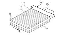
図1は、本発明の一実施の形態であるフロントライト(面発光装置)の構成を示す部分斜視図である。また、図2は、図1に示すフロントライト10から、カバー部材18を取り外した状態を示す部分斜視図である。これらの図に示すフロントライト10は、透明な樹脂材料からなる平板状の導光板12と、この導光板12の側端面12a側の側端部(長方形状の導光板12の短辺側の一端部)に配された棒状のバー導光体(導光体)13と、バー導光体13の長さ方向の両端部に配設された発光素子(光源)15,15と、前記バー導光体13及び発光素子15,15並びに導光板12のバー導光体13側の側端部を覆うように被着されたカバー部材18とを備えて構成されている。
【0026】
導光板12は、図1に示すように透明な平板状の部材であり、バー導光体13と対向する側端面12aを入光面とし、上面が側端面12aとほぼ平行な側面視くさび型の凸部14がストライプ状互いに平行に形成された反射面12cとされている。この導光板12は、側端面12aから内部に導入された光を、反射面12cで反射させてその伝搬方向を変え、反射面12cの反対側の面(図示下面)から出射させる構造とされている。
また、導光板12は、透明なアクリル樹脂などの樹脂材料を平板状に射出成形する方法などにより作製することができる。また、導光板12を構成する材料としてはアクリル系樹脂のほか、ポリカーボネート系樹脂、エポキシ樹脂などの透明な樹脂材料や、ガラスなどを用いることができる。また、具体的な例を挙げるならば、特に限定されるものではないが、アートン(商品名:JSR社製)や、ゼオノア(商品名:日本ゼオン社製)などを好適なものとして挙げることができる。
【0027】
バー導光体13は、図1及び図2に示すように、アクリル系樹脂やポリカーボート系樹脂などからなる四角柱状の透明の部材であり、このバー導光体13の長さ方向両端部にLED(白色LED)からなる発光素子15,15が配設されている。この導光体13の側面のうち、導光板12と反対側の側面は、図2に示すように、複数(図示では7本)のくさび状の溝16がストライプ状に形成された反射面13bとされており、溝16の方向は発光素子15が設けられた端面と平行とされている。そして、バー導光体13は、発光素子15,15から出射されて内部に導入された光を、この溝16を構成する面で反射させることで、導光板12側へ光の伝搬方向を変え、導光板12の側端面12aに光を照射するようになっている。バー導光体13から導光板12内へ導入された光は、導光板12の内部を伝搬し、反射面12cに形成された凸部14を構成する面で反射されて、その伝搬方向を変えられ、導光板12の出射面(図示下面)から出射されるようになっている。
【0028】
発光素子15は、本実施形態のフロントライト10ではLEDからなるものとしたが、これに限定されるものではなく、バー導光体13の両端部に実装可能な発光素子であれば問題なく適用することができ、例えばEL(Electro Luminescence)素子等の発光素子も適用することができる。また、この発光素子15は、バー導光体13の厚さ方向のほぼ中心に発光素子15の発光領域の中心が位置するようにバー導光体13の端面に配置することが好ましい。このような位置に配置することで、バー導光体13の反射面13b以外の側面へ入射する光量を低減することができ、バー導光体13から出射される光の均一性を高めることができる。
【0029】
カバー部材18は、図1に示すようにバー導光体13と、その両端の発光素子15,15と、導光板12のバー導光体13側の側端部を覆って配設された断面コ字型の金属製の部材である。このカバー部材18は、導光板12の反射面側(図示上面側)に配置された部位である反射面カバー部18aと、導光板12の出射面側(図示下面側)に配置された部位である出射面カバー部18bと、これらの基端部に接続されるとともにバー導光体13の反射面13bと対向して配置された導光体カバー部18とを備えて構成されている。
【0030】
また、図3は本実施形態に係るカバー部材18がバー導光体13と発光素子15に被着されている状態を説明するための拡大説明図である。この図に示すように、本実施形態に係るカバー部材18では、導光板12の側面から突出されている発光素子15を覆うために、発光素子15の外面側(バー導光体13と対向する面と反対側の面)と対向するように外面カバー部18dと、発光素子15の導光板12側の側面と対向するように側面カバー部18eが形成されている。これら外面カバー部18dと側面カバー部18eは、それぞれ反射面カバー部18a、出射面カバー部18b、導光体カバー部18との間に間隙が形成されないようにすることが好ましい。尚、外面カバー部18dは、発光素子15の外面側が遮光されており、カバー部材18の外側に光が漏洩しないようにされている場合には設けなくともよい。
【0031】
また、前記側面カバー部18eは、本実施形態のフロントライト10においては、導光板12とバー導光体13との配置の位置決め機構を兼ねるように構成されており、2つの側面カバー部18e,18eの間に導光板12を挿入するのみで、バー導光体13の側面へ正確に位置決めできるようになっている。
【0032】
本実施形態に係るカバー部材18の特徴的な点は、図1に示すように反射面カバー部18aの導光方向(バー導光体13から導光板12へ向かう方向)への長さが、出射面カバー部18bの導光方向への長さよりも導光方向へ突出されて形成されており、この突出長さLが、0.5mm以上とされている点である。このような構成とすることで、本実施形態のフロントライト10は、大幅な輝度の向上を実現している。また、前記突出長さLは、0.7mm以上とすることが好ましく、0.8mm以上とすることがより好ましい。このような範囲とすることで、さらなる輝度の向上を実現することができる。この作用について図4及び図5を参照して以下に詳細に説明する。
【0033】
図4は、図1〜図3に示すフロントライト10のB−B線に沿う部分側断面図であり、図5は、図13に示すフロントライトのC−C線に沿う部分側断面図である。
まず、図5に示す従来の構成においては、断面コ字型のカバー部材118が、バー導光体113を内側に収納して導光板112の側端部を上下から把持して構成されており、カバー部材118の導光方向への長さは、導光板112の反射面112c側と、出射面112b側でほぼ同等の長さとされている。この構造では、図5に示すように出射面カバー部118bの先端部内面側で反射された導光板12内を伝搬する光は、導光板112の反射面112cからフロントライトの上方へ出射される。この光は、仮にフロントライトの下面側に液晶表示ユニット200が配置されているとするならば、液晶表示ユニット20を経由せずに使用者に至る光であり、液晶表示ユニット200の表示に寄与しないのは勿論のこと、導光板112の反射面112cに白化現象を生じさせて視認性低下の原因となる。
【0034】
一方、図4に示す本実施形態のフロントライト10では、断面コ字型のカバー部材18はバー導光体13を内側に収納するとともに、その先端部で導光板12を図示上下方向に把持している。そして、導光板12の反射面12c側(図示上側)の反射面カバー部18aの導光方向への長さが、導光板12の出射面12b側の出射面カバー部18bの導光方向への長さよりも突出長さLだけ長くなるように形成されている。このような構成のフロントライト10においては、バー導光体13から出射された光は、導光板12の内面あるいはカバー部材18の内面側で反射を繰り返しながら、導光体13側から導光板12側へ向かう方向へ伝搬する。本実施形態のフロントライト10では、図4に示すように、このカバー部材18の内面側で反射される光のうち、出射面カバー部18bの先端部内面側で反射された光が、反射面カバー部18aの先端部の内面側でさらに反射され、導光板12bの出射面12bからフロントライト10の下方へ出射されるので、例えば図4に示すようにフロントライト10の下面側に液晶表示ユニット20を配置するならば、この反射面カバー部18aの先端部で反射された光も液晶表示ユニット20の表示に寄与する光として利用される。このように、本実施形態のフロントライト10は、導光板12の出射面12bからの出射光量を増加させることができるとともに、導光板12の反射面12cからの光の漏洩を抑制することができるので、図5に示す従来のフロントライトに比して大幅な輝度を実現し、かつ白化現象が生じ難い、視認性に優れるフロントライトとされている。
【0035】
本実施形態のフロントライト10においては、図4に示すカバー部材18の内面側に、AlやAgなどの光反射性に優れた金属薄膜からなる反射層を形成することができる。このような反射層を形成すれば、導光体13や導光板12の内部からカバー部材18へ入射する光をほとんど減衰させることなくバー導光体13、導光板12へ反射させて戻すことができる。このようにしてバー導光体13、導光板12内へ戻された光は、導光板12の出射面12bから出射される照明光として利用することができ、その結果、フロントライト10の輝度を高めることができる。
【0036】
また、本実施形態のフロントライト10においては、バー導光体13の構成を適切なものとすることにより、出射光量の均一化を実現している。このバー導光体13の構成について図6〜図8を参照して以下に詳細に説明する。
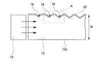
図6は、図2に示すバー導光体13と発光素子15とを拡大して示す部分平面図であり、図7は図6に示す領域Aを拡大して示す構成図である。
【0037】
本実施形態に係るバー導光体13の反射面13bには、図2に示すように複数のくさび状の溝16が形成されており、これらの溝16は、図7に示すようにバー導光体13の出射面13aに対して傾斜して形成された2つの斜面部16a、16bから構成され、これらの斜面部16a、16bどうしが成す角度αは、105度以上115度以下とされている。これは、角度αが105度未満の場合には、望ましい方向への出射光が得られず、結果として輝度が低下するので好ましくなく、αが115度を超える場合には、出射光量の分布の均一性が保てない結果となり好ましくないからである。また、前記角度αは、108度以上112度以下とすることがより好ましい。このような範囲とするならば、導光板12方向へ出射される光量をより増加させることができ、フロントライト10の輝度をさらに高めることができる。
【0038】
また、図6及び図7に示すように、本実施形態に係るバー導光体13の反射面13bには、AlやAg等の高反射率の金属薄膜からなる反射層19が形成されている。この反射層19が形成されていることで、反射面13bからの光の漏洩を防止できるとともに、溝16の斜面部16a、16bにおける光の反射率を高めることができ、導光板12へ出射される光量を増加させることができる。この反射層19の膜厚は、30nm以上200nm以下とされることが好ましく、前記反射層の膜厚が、50nm以上150nm以下とされることがより好ましい。反射層の膜厚が30nm未満であると、反射層を透過して光が漏洩して面発光装置の輝度低下の原因となり、200nmを越える場合には、反射層の成膜に時間がかかるために生産性が低下することとなる。また、50nm以上150nmの範囲とすれば、良好な光反射性を備えた反射層を容易に形成することができ、高輝度の面発光装置を容易に製造することができる。
【0039】
本実施形態のフロントライト10においては、反射面13bに形成されている溝16は、斜面部16a、16bの成す角度が前記範囲とされているが、図7に示すその溝深さDも所定の深さに制御されて構成されている。この溝16の深さDについて図8を参照して以下に詳細に説明する。図8は、導光体13の反射面13bに形成された溝16の深さDと、発光素子15とそれぞれの溝16との距離との関係を示すグラフである。図8では、導光体13の中央から一方の発光素子15までの溝16の深さを示したが、他方の発光素子15までの距離と溝深さDとの関係は、導光体13の中央に対して対象となっている。すなわち、導光体13の中央からの距離が等しい二つの溝16の深さDは、同一とされている。
【0040】
本実施形態の面発光装置10における溝16の深さDは、図8に示すように、導光体13の中央部の近傍である領域1と、この領域1の外側から発光素子15までの領域2とで異なるように形成されている。すなわち、導光体13の中央部側の領域2では、溝16の深さDは深さd2で一定になるように形成されており、領域1では、発光素子15に最も近い溝16では深さd1とされ、導光体13の中央に近い溝16ほど深くなるように形成されている。そして、この領域1における発光素子15から溝16までの距離と、溝16の深さDとの関係が、二次関数または指数関数となるように形成されている。つまり、ある一つの溝16の深さDは、発光素子15からの距離tを用いて、D=at2+bt+d1(a、bは定数)またはD=cet+d1(cは定数)なる関係式で表すことができ、これらの関係式に含まれる定数は、導光体13の長さ等の寸法により適宜最適な値に調整すればよい。より具体的には、導光体13の長さが40mm〜100mm程度であれば、図4に示す溝深さd1を20μm程度、d2を50μm程度とし、領域1において、発光素子15側から導光体13の中央へ溝深さDが20μmから順次二次関数的又は指数関数的に増加するように形成すればよい。
【0041】
また、図6に示す導光体13の反射面13bから出射面13aまでの距離Wは、3.2mm以上5.0mm以下とすることが好ましい。この距離Wが3.2mm未満では、導光体の両端部が明るく、中央部が暗くなり、5.0mmを越えると、フロントライト10としての出射光量が低下し、輝度が全体として低下するためである。
【0042】
このように本実施形態のフロントライト10は、バー導光体13が上記のように制御されて構成されていることで、バー導光体13から導光板12内へ導入される光量を増加させることができるとともに、その均一性も向上されている。これにより、導光板12の出射面から出射される光量の増加と、出射光の均一性の向上を実現することができる。そして、上述の構成のカバー部材18が設けられていることで、導光板12の上面(反射面12c)から光が漏洩するのを抑制するとともに、従来上面へ漏洩していた光を導光板12の下面側へ出射させることで、フロントライトの輝度の向上を実現している。
【0043】
(液晶表示装置)
次に、上記実施の形態のフロントライト10を備えた液晶表示装置について説明する。図9は、図1に示すフロントライト10を備えた液晶表示装置の一例を示す斜視図であり、図10は、図9に示すD−D線に沿う模式断面図である。これらの図に示す液晶表示装置は、本実施形態のフロントライト10と、その背面側に配置された液晶表示ユニット20とから概略構成されている。
【0044】
フロントライト10の構成の説明は、図1に示すフロントライト10と同様なので省略するが、図10に示すように導光板12の下面(液晶表示ユニット20側)は光が出射される出射面12bとされている。この出射面12bと反対側の面(導光板12の上面)は、導光板12の内部にて光の方向を変えるために出射面12bに対して傾斜して形成された第1の斜面部14aと、これに続く第2の斜面部14bとからなる側面くさび状の凸部14が、周期的に配置された反射面12cとされている。
【0045】
液晶表示ユニット20は、図10に示すように、液晶層23を挟持して対向する第1の基板21と第2の基板22をシール材24で接合一体化した構成であり、第1の基板21の液晶層23側には、電極層や配向膜を含み、液晶層23を駆動制御するための表示回路27が形成され、第2の基板22の液晶層23側には、液晶表示ユニット20に入射した光を反射させるための反射膜25と、電極層や配向膜を含み液晶層23を駆動制御するための表示回路26とが順に積層形成されている。また、反射膜25は、反射した光を拡散させるために表面に凹凸形状を付して構成することができる。
【0046】
上記構成の液晶表示装置において、発光素子15から出射された光は、まず導光体13の内部に導入され、導光体13の反射面13bで反射されてその伝搬方向を変えられ、導光板13の出射面と対向して配置された導光板12の側端面から導光板12内へ導入される。そして、導光板12内部を伝搬する光が、導光板の反射面12cの斜面部14aで反射されることで、その伝搬方向を変えられ、導光板12の出射面12bから液晶表示ユニット20を照明する光が出射されるようになっている。
【0047】
次に、液晶表示ユニット20に入射した光は、第1の基板21、表示回路27、液晶層23、表示回路26を透過して反射膜25へ到達し、反射膜25により反射されて再び液晶層23側へ戻される。そして、この反射された光が、液晶表示ユニット20の上面側から出射され、導光板12を透過して使用者へ到達するようになっている。このように、本発明の液晶表示装置は、反射型の液晶表示ユニット20の光源として本発明に係るフロントライト10を用いることで、十分な外光が得られない暗所などにおいても表示を視認することができるようになっている。また、本発明に係るフロントライト10を備えていることで、液晶表示ユニット20へ照射される光量を多くすることができるので、高輝度の表示を得ることができる。また、フロントライト10の上面側への光の漏洩が押さえられているので、白化現象による視認性の低下が抑制されている。
【0048】
【実施例】
以下実施例を参照して本発明をより詳細に説明し、本発明の効果をより明らかにするが、本発明は以下の実施例に限定されるものではない。
【0049】
本例では、図1に示すフロントライト10を基本構成とし、カバー部材18の導光板12上面側における突出長さLを種々に変えたフロントライトを作製した。これらのフロントライトの構成を表1に示す。本例で作製したフロントライトでは、発光素子15として白色LEDを用い、導光板12は、アクリル樹脂を成型して作製した50mm×40mm×0.7mmの平板状のものを用いた。また、バー導光体13の反射面13bに形成された溝16の深さは、発光素子15に最も近い溝の深さを20μmとし、バー導光体13の中央部からの距離が3mm以下の溝16については、その深さを50ミクロンで一定とした。そして、発光素子15側の溝からバー導光体13の中央部に向かって、指数関数的に溝16の深さが深くなるように形成した。
【0050】
【表1】
次に、上記にて作製したフロントライトを動作させ、導光板12の出射面(図示下面)から出射された光が液晶表示ユニット20に入射し、反射膜25で反射されて使用者に到達する際の出射光量(すなわち、液晶表示装置の表示輝度)とその分布を測定した。測定には、色彩輝度計BM5A(商品名:トプコン社製)を用いた。その測定結果を表1に併記する。
表1に示すように、バー導光体13の形状が本発明の要件を満たす試料1〜5のフロントライトは、バー導光体13の形状が本発明の要件を満たさない比較試料1のフロントライトと比較して、輝度が大幅に改善されており、また輝度の分布も小さくなっており、高輝度で均一な照明が可能なフロントライトであることがわかる。
【0052】
【発明の効果】
以上、詳細に説明したように、本発明の面発光装置は本発明の面発光装置は、導光板と、該導光板の一側端面に沿って配置された導光体と、該導光体の両端に配設された光源とを備え、前記導光板の一面側が、内部を伝搬する光を反射させるために凹凸の形状が形成された反射面とされ、前記導光板の他面側が、前記反射面により反射された光を出射させるための出射面とされており、前記導光板の反射面側の側端部を覆う反射面カバー部と、前記導光体を覆う導光体カバー部と、前記導光板の出射面側の側端部を覆う出射面カバー部と、前記光源の前記導光体と対向する面と反対側の面と対向するように形成された外面カバー部と、前記光源の前記導光板側の側面と対向するように形成された側面カバー部とを有するカバー部材が、少なくとも前記導光体と、前記導光板の側端部とを覆うように被着され、前記反射面カバー部の、導光体側から導光板側への突出長さが、前記出射面カバー部の導光体側から導光板側への突出長さより0.5mm以上長く形成されたことで、導光板の反射面から光の漏洩を防止することができるので、光源の利用効率を高め、面発光装置の輝度を向上させることができる。また、導光板の反射面側への光の漏洩が抑制されることで、前記白化現象も効果的に抑制することができる。
また、前記導光体の前記導光板の側端面と対向する側面が、前記光源の光を前記導光板に照射するための出射面とされ、該出射面と反対側の側面が、内部を伝搬する光を反射させるための対になる斜面を有する凹状の溝が所定のピッチで周期的に形成された反射面とされており、前記凹状の溝の深さが、前記光源側の溝よりも導光体の中央部の溝ほど徐々に深く形成されているので、導光体から出射される光を効率よく導光板に供給し、また導光体から出射される光の均一性を高めて、導光板の主面から出射される光量と、その均一性を高めることができる。
【0053】
また、本発明の面発光装置は、導光板と、該導光板の一側端面に沿って配置された導光体と、該導光体の両端に配設された光源とを備え、前記導光板の一面側が、内部を伝搬する光を反射させるために凹凸の形状が形成された反射面とされ、前記導光板の他面側が、前記反射面により反射された光を出射させるための出射面とされており、少なくとも前記導光体と、前記導光板の側端部に、導光体及び導光板の内部を伝搬する光を反射させるための金属薄膜からなる反射膜が形成され、前記導光体が配設された導光板の側端面側からの反射膜の長さが、前記導光板の反射面側の方が前記導光板の出射面側よりも0.5mm以上長く形成された構成も適用することができ、この構成によっても上記カバー部材を備えた面発光装置と同様の効果を得ることができる。
【0054】
次に、本発明の面発光装置において、前記導光体の導光板の側端面と対向する側面が、前記光源の光を導光板に照射するための出射面とされ、該出射面と反対側の側面が、内部を伝搬する光を反射させるための対になる斜面を有する凹状の溝が所定のピッチで周期的に形成された反射面とされており、前記凹状の溝の深さが、前記光源側の溝よりも導光体の中央部の溝ほど深く形成され、前記溝を構成する2つの斜面の成す角度が、105度以上115度以下とされた構成とするならば、導光体から出射される光を効率よく導光板に供給し、また導光体から出射される光の均一性を高めて、導光板の主面から出射される光量と、その均一性を高めることができる。
【0055】
次に、本発明に係る液晶表示装置は、本発明に係る面発光装置を、液晶表示ユニットの前面に備えたことで、上記面発光装置により液晶表示ユニットを均一、かつ高輝度で照明することができるので、優れた視認性を備えた液晶表示装置である。
【図面の簡単な説明】
【図1】 図1は、本発明の一実施の形態であるフロントライトの部分斜視図である。
【図2】 図2は、図1に示すフロントライトのカバー部材を取り外した状態を示す部分斜視図である。
【図3】 図3は、図1に示すフロントライトのカバー部材周辺を拡大して示す部分斜視図である。
【図4】 図4は、図1に示すフロントライトのB−B線に沿う部分断面図である。
【図5】 図5は、従来の構成のフロントライトの部分断面図である。
【図6】 図6は、図1に示すバー導光体の部分平面図である。
【図7】 図7は、図6に示す領域Aを拡大して示す部分平面図である。
【図8】 図8は、図1,2に示すバー導光体に形成された溝の深さと、光源からの距離との関係を示すグラフである。
【図9】 図9は、図1に示す本実施形態のフロントライトを備えた液晶表示装置の一例を示す斜視図である。
【図10】 図10は、図10に示す液晶表示装置のB−B線に沿う模式断面図である。
【図11】 図11は、従来のフロントライトの構成の一例を示す斜視図である。
【図12】 図12は、従来のフロントライトの構成の他の例を示す斜視図である。
【図13】 図13は、従来のフロントライトの構成のさらに他の例を示す斜視図である。
【符号の説明】
10 フロントライト(面発光装置)
12 導光板
13 バー導光体(導光体)
13a (導光体の)出射面
13b (導光体の)反射面
15 発光素子(光源)
16 溝
18 カバー部材
18a 反射面カバー部
18b 出射面カバー部
18c 導光体カバー部
19 反射層
20 液晶表示ユニット[0001]
BACKGROUND OF THE INVENTION
The present invention relates to a surface light emitting device and a liquid crystal display device, and more particularly to a structure of a surface light emitting device for using more of light emitted from a light source as illumination light.
[0002]
[Prior art]
Conventionally, in a reflective liquid crystal display device that displays using ambient light as a light source, the brightness depends on the amount of ambient light, so in environments where sufficient ambient light cannot be obtained, such as when used in a dark place, There has been a problem that the visibility of the display is extremely lowered. Therefore, a liquid crystal display device of a type in which a front light (surface light emitting device) is provided on the front side of a reflective liquid crystal display unit (liquid crystal display element) and used as an auxiliary light source has been proposed. The liquid crystal display device equipped with this front light operates as a normal reflection type liquid crystal display device in an environment where sufficient ambient light can be obtained such as outdoors in the daytime, and the front light is turned on as a light source if necessary. It is. A configuration example of such a front light will be described below with reference to FIGS.
[0003]
The
[0004]
The
[0005]
However, since the
In this
[0006]
Accordingly, in the
As described above, the
[0007]
[Problems to be solved by the invention]
Although the
[0008]
According to the front light 130 having such a configuration, it is possible to suppress a decrease in luminance due to loss due to light leakage in directions other than the light guide direction, and thus it is possible to perform illumination with higher luminance than the
[0009]
Accordingly, an object of the present invention is to provide a surface light emitting device that has high light source utilization efficiency, high brightness, and excellent uniformity of emitted light.
Another object of the present invention is to provide a liquid crystal display device having a surface light emitting device having the above-described excellent characteristics and excellent visibility.
[0010]
[Means for Solving the Problems]
In order to achieve the above object, the present invention employs the following configuration.
The surface light-emitting device of the present invention includes a light guide plate, a light guide disposed along one side end face of the light guide plate, and light sources disposed at both ends of the light guide. One surface side is a reflecting surface formed with an uneven shape to reflect light propagating inside, and the other surface side of the light guide plate is an emitting surface for emitting light reflected by the reflecting surface. A reflecting surface cover portion covering a side end portion on the reflecting surface side of the light guide plate, a light guide cover portion covering the light guide body, and an exit surface covering a side end portion on the exit surface side of the light guide plate. A cover part;An outer surface cover portion formed to face a surface opposite to a surface facing the light guide of the light source; and a side cover portion formed to face a side surface of the light source on the light guide plate side. HaveA cover member is attached so as to cover at least the light guide and a side end portion of the light guide plate, and the reflection surface cover portion protrudes longer in the light guide direction than the emission surface cover portion. Formed,The side surface of the light guide opposite to the side end surface of the light guide plate is an emission surface for irradiating the light guide plate with light from the light source, and the side surface opposite to the emission surface is light propagating inside. A concave groove having a pair of slopes for reflecting light is formed as a reflection surface periodically formed at a predetermined pitch, and the depth of the concave groove is more light-guiding than the light source side groove. The groove in the center of the body is gradually formed deeperIt is characterized by that.
[0011]
In the surface light emitting device according to the present invention, the length of the reflection surface cover portion of the cover member that covers the light guide and the side end portions of the light guide plate is made larger than that of the emission surface cover portion, so that the light guide plate is guided inside the light guide plate. More light is propagated to the exit surface side of the optical plate. This structure can prevent light leakage from the reflection surface of the light guide plate, so that the light source utilization efficiency can be improved and the luminance of the surface light emitting device can be improved. In addition, since the light leakage to the reflection surface side of the light guide plate is suppressed, the whitening phenomenon can be effectively suppressed.
[0012]
Next, in the surface light emitting device of the present invention, it is preferable that the reflection surface cover portion is formed to protrude longer than the emission surface cover portion by 0.5 mm or more in the light guide direction, and protrudes by 0.7 mm or more. More preferably it is formed.
[0013]
By setting the difference in the protruding length within the above range, the amount of light propagating to the exit surface side of the light guide plate can be further increased, so that the luminance of the surface light emitting device can be further increased. In addition, this inventor verifies that the said range is appropriate in the below-mentioned Example.
[0014]
Next, the surface light emitting device of the present invention can be configured such that a reflective layer made of a metal thin film is formed on the inner surface side of the cover member. By adopting such a configuration, light incident on the cover member from the light guide or the light guide plate can be reflected back to the light guide or the light guide plate while suppressing its loss. Can be increased.
[0015]
Next, the surface light-emitting device of the present invention includes a light guide plate, a light guide disposed along one side end surface of the light guide plate, and light sources disposed at both ends of the light guide, One surface side of the light guide plate is a reflection surface formed with a concavo-convex shape to reflect light propagating inside, and the other surface side of the light guide plate is an output for emitting the light reflected by the reflection surface A reflection film made of a metal thin film for reflecting light propagating through the light guide and the inside of the light guide plate is formed on at least the light guide and a side end portion of the light guide plate, In the length of the reflective film from the side end surface side of the light guide plate on which the light guide is disposed, the length of the reflective surface side of the light guide plate is longer than the length of the light output surface side of the light guide plate It is characterized by.
[0016]
In the surface light emitting device according to the present invention, the above-described configuration is also applicable. That is, in order to prevent light leakage at the side end of the light guide, the light source, or the light guide plate, a reflective film made of a metal thin film is formed on these surfaces. With such a configuration, it is possible to prevent light leakage and to suppress light loss during reflection on the reflective film surface, so that the light from the light source can be used efficiently.
[0017]
Next, the surface light-emitting device of the present invention may have a configuration in which an antireflection layer is formed on one or both of the light guide plate side end face and the light guide side face where the light guide plate and the light guide face each other. it can. By adopting such a configuration, when light is introduced from the light guide to the light guide plate, it is possible to prevent the light from being reflected from the side end face of the light guide plate and returning to the light guide side, thereby achieving higher brightness. The surface light emitting device can be realized. That is, when light is reflected by the side end face of the light guide plate, the light returning to the light guide side is reflected by the reflection surface of the light guide and enters the light guide plate again. Since such light is light in an unintended direction in the design of the light guide, if this light is emitted from the light guide plate, the uniformity of the amount of emitted light may be reduced, and should be eliminated as much as possible. However, such a configuration can eliminate such reflected light.
[0018]
Next, in the surface light-emitting device of the present invention, the side surface of the light guide opposite to the side end surface of the light guide plate is an emission surface for irradiating the light guide plate with light from the light source, and is opposite to the emission surface. The side surface of the groove is a reflecting surface in which concave grooves having a pair of inclined surfaces for reflecting light propagating through the inside are periodically formed at a predetermined pitch, and the depth of the concave groove is It is preferable that the groove at the center of the light guide is formed deeper than the groove on the light source side, and the angle formed by the two slopes constituting the groove is 105 degrees or more and 115 degrees or less.
[0019]
In the surface light emitting device of this configuration, the shape of the concave groove that affects the uniformity of the light emitted from the light guide to increase the uniformity of the light emitted from the light guide to the side end surface of the light guide plate. , As described above, the light emitted from the light guide is efficiently supplied to the light guide plate, and the uniformity of the light emitted from the light guide is improved, from the main surface of the light guide plate. The amount of emitted light and its uniformity are improved. Further, in the surface light emitting device of this configuration, the depth of the concave groove is formed deeper as the groove is closer to the central portion of the light guide. By setting it as such a structure, distribution of the emitted light quantity in the length direction of a light guide can be equalize | homogenized.
[0020]
Further, the angle formed by the two inclined surfaces constituting the concave groove is set to 105 degrees or more and 115 degrees or less. By setting it as such a range, the light quantity radiate | emitted to a light-guide plate direction can be increased, the utilization efficiency of a light source can be improved, and a surface-emitting device with high brightness | luminance can be implement | achieved. If the angle is less than 105 degrees, emitted light in a desired direction cannot be obtained, resulting in a decrease in luminance. If it exceeds 115 degrees, the uniformity of the amount of emitted light cannot be maintained, which is not preferable.
[0021]
Next, in the surface light-emitting device of the present invention, it is preferable that an angle formed by two inclined surfaces constituting the concave groove is 108 degrees or more and 112 degrees or less. By setting the angle in such a range, the amount of light emitted toward the light guide plate can be further increased, and the luminance of the surface light emitting device can be increased.
[0022]
Next, in the surface light-emitting device of the present invention, it is preferable that the distance between the emission surface and the reflection surface of the light guide is 3.2 mm or more and 5.0 mm or less. By setting the distance between the exit surface and the reflecting surface of the light guide in such a range, the light introduced from the light guide to the light guide plate is prevented from leaking from the main surface of the light guide plate. The luminance of the light emitting device can be increased.
[0023]
Next, in the surface light-emitting device of the present invention, it is preferable that the center of the light-emitting portion of the light source is disposed substantially at the center in the thickness direction of the light guide. It is preferable that the light guide is disposed substantially at the center in the thickness direction. With such a configuration, the uniformity of the light emitted from the light guide can be increased, and the uniformity of the emitted light amount is not impaired even when a large-area light guide plate is used.
[0024]
Next, a liquid crystal display device of the present invention is characterized in that any one of the surface light emitting devices described above is provided on the front surface of a liquid crystal display unit. According to such a configuration, the liquid crystal display unit can be illuminated uniformly and with high luminance by the surface light emitting device, and thus a liquid crystal display device having excellent visibility can be provided.
[0025]
DETAILED DESCRIPTION OF THE INVENTION
Hereinafter, embodiments of the present invention will be described with reference to the drawings, but the present invention is not limited to the following embodiments.
FIG. 1 is a partial perspective view showing a configuration of a front light (surface emitting device) according to an embodiment of the present invention. FIG. 2 is a partial perspective view showing a state where the
[0026]
The
The
[0027]
As shown in FIGS. 1 and 2, the
[0028]
The
[0029]
As shown in FIG. 1, the
[0030]
FIG. 3 is an enlarged explanatory view for explaining a state in which the
[0031]
Further, the
[0032]
A characteristic point of the
[0033]
4 is a partial side sectional view taken along line B-B of the front light 10 shown in FIGS. 1 to 3, and FIG. 5 is a partial side sectional view taken along line C-C of the front light shown in FIG. 13. is there.
First, in the conventional configuration shown in FIG. 5, a
[0034]
On the other hand, in the
[0035]
In the
[0036]
Further, in the
6 is a partial plan view showing the
[0037]
A plurality of wedge-shaped
[0038]
As shown in FIGS. 6 and 7, a
[0039]
In the
[0040]
As shown in FIG. 8, the depth D of the
[0041]
Moreover, it is preferable that the distance W from the
[0042]
Thus, the
[0043]
(Liquid crystal display device)
Next, a liquid crystal display device including the
[0044]
The description of the configuration of the
[0045]
As shown in FIG. 10, the liquid
[0046]
In the liquid crystal display device having the above configuration, the light emitted from the
[0047]
Next, the light incident on the liquid
[0048]
【Example】
Hereinafter, the present invention will be described in more detail with reference to examples, and the effects of the present invention will be clarified. However, the present invention is not limited to the following examples.
[0049]
In this example, the front light 10 shown in FIG. 1 was used as a basic configuration, and front lights having various protrusion lengths L on the upper surface side of the
[0050]
[Table 1]
Next, the front light produced above is operated, and the light emitted from the emission surface (the lower surface in the drawing) of the
As shown in Table 1, the front lights of Samples 1 to 5 where the shape of the
[0052]
【The invention's effect】
As described above in detail, the surface light-emitting device of the present invention includes a light guide plate, a light guide disposed along one end face of the light guide plate, and the light guide. A light source disposed at both ends of the light guide plate, wherein one surface side of the light guide plate is a reflective surface formed with a concavo-convex shape to reflect light propagating inside, and the other surface side of the light guide plate is A light output surface for emitting light reflected by the reflection surface; a reflection surface cover portion covering a side end portion of the light guide plate on the reflection surface side; and a light guide body cover portion covering the light guide body; , An exit surface cover portion covering a side end portion on the exit surface side of the light guide plate;An outer surface cover portion formed to face a surface opposite to the surface facing the light guide of the light source, and a side cover portion formed to face a side surface of the light source on the light guide plate side. WhenA cover member is attached so as to cover at least the light guide body and a side end portion of the light guide plate, and the projection length of the reflective surface cover portion from the light guide body side to the light guide plate side is Since the emission surface cover portion is formed to be longer by 0.5 mm or more than the protruding length from the light guide side to the light guide plate side, light leakage from the reflection surface of the light guide plate can be prevented. And the luminance of the surface light emitting device can be improved. In addition, since the light leakage to the reflection surface side of the light guide plate is suppressed, the whitening phenomenon can be effectively suppressed.
In addition, a side surface of the light guide opposite to the side end surface of the light guide plate is an emission surface for irradiating the light guide plate with light from the light source, and a side surface opposite to the emission surface propagates inside. A concave groove having a pair of inclined surfaces for reflecting light to be reflected is a reflection surface formed periodically at a predetermined pitch, and the depth of the concave groove is larger than that of the groove on the light source side. Since the groove at the center of the light guide is gradually formed deeper, the light emitted from the light guide is efficiently supplied to the light guide plate, and the uniformity of the light emitted from the light guide is increased. The amount of light emitted from the main surface of the light guide plate and its uniformity can be improved.
[0053]
The surface light-emitting device of the present invention includes a light guide plate, a light guide disposed along one side end surface of the light guide plate, and light sources disposed at both ends of the light guide. One surface side of the light plate is a reflection surface formed with an uneven shape to reflect light propagating inside, and the other surface side of the light guide plate is an emission surface for emitting the light reflected by the reflection surface A reflection film made of a metal thin film for reflecting light propagating through the light guide and the inside of the light guide plate is formed at least on the side of the light guide and the light guide plate. A structure in which the length of the reflection film from the side end surface side of the light guide plate on which the light body is disposed is formed so that the reflection surface side of the light guide plate is longer by 0.5 mm or more than the emission surface side of the light guide plate This structure also has the same effect as the surface light emitting device having the cover member. Rukoto can.
[0054]
Next, in the surface light-emitting device of the present invention, the side surface of the light guide opposite to the side end surface of the light guide plate is an exit surface for irradiating the light guide plate with light from the light source, and is opposite to the exit surface. The side surface of the groove is a reflecting surface in which concave grooves having a pair of inclined surfaces for reflecting light propagating through the inside are periodically formed at a predetermined pitch, and the depth of the concave groove is If the groove at the center of the light guide is formed deeper than the groove on the light source side, and the angle formed by the two inclined surfaces constituting the groove is 105 degrees or more and 115 degrees or less, the light guide The light emitted from the body can be efficiently supplied to the light guide plate, and the uniformity of the light emitted from the light guide can be increased to increase the amount of light emitted from the main surface of the light guide plate and the uniformity thereof. it can.
[0055]
Next, in the liquid crystal display device according to the present invention, the surface light emitting device according to the present invention is provided on the front surface of the liquid crystal display unit, so that the liquid crystal display unit is illuminated uniformly and with high luminance by the surface light emitting device. Therefore, the liquid crystal display device has excellent visibility.
[Brief description of the drawings]
FIG. 1 is a partial perspective view of a front light according to an embodiment of the present invention.
FIG. 2 is a partial perspective view showing a state where a cover member of the front light shown in FIG. 1 is removed.
3 is an enlarged partial perspective view showing the periphery of a cover member of the front light shown in FIG. 1. FIG.
4 is a partial cross-sectional view taken along line BB of the front light shown in FIG. 1. FIG.
FIG. 5 is a partial sectional view of a front light having a conventional configuration.
FIG. 6 is a partial plan view of the bar light guide shown in FIG. 1;
FIG. 7 is an enlarged partial plan view showing a region A shown in FIG. 6;
FIG. 8 is a graph showing the relationship between the depth of the groove formed in the bar light guide shown in FIGS. 1 and 2 and the distance from the light source.
FIG. 9 is a perspective view showing an example of a liquid crystal display device including the front light of the present embodiment shown in FIG.
FIG. 10 is a schematic cross-sectional view taken along line BB of the liquid crystal display device shown in FIG.
FIG. 11 is a perspective view showing an example of a configuration of a conventional front light.
FIG. 12 is a perspective view showing another example of the configuration of a conventional front light.
FIG. 13 is a perspective view showing still another example of the configuration of a conventional front light.
[Explanation of symbols]
10 Front light (surface emitting device)
12 Light guide plate
13 Bar light guide (light guide)
13a (light guide) exit surface
13b Reflecting surface (of light guide)
15 Light emitting element (light source)
16 groove
18 Cover member
18a Reflecting surface cover
18b Outgoing surface cover
18c Light guide cover part
19 Reflective layer
20 Liquid crystal display unit
Claims (11)
Translated fromJapanese前記導光板の一面側が、内部を伝搬する光を反射させるために凹凸の形状が形成された反射面とされ、前記導光板の他面側が、前記反射面により反射された光を出射させるための出射面とされており、
前記導光板の反射面側の側端部を覆う反射面カバー部と、前記導光体を覆う導光体カバー部と、前記導光板の出射面側の側端部を覆う出射面カバー部と、前記光源の前記導光体と対向する面と反対側の面と対向するように形成された外面カバー部と、前記光源の前記導光板側の側面と対向するように形成された側面カバー部とを有するカバー部材が、少なくとも前記導光体と、前記導光板の側端部とを覆うように被着され、
前記反射面カバー部が、前記出射面カバー部よりも導光方向先方側へ長く突出して形成され、
前記導光体の前記導光板の側端面と対向する側面が、前記光源の光を前記導光板に照射するための出射面とされ、該出射面と反対側の側面が、内部を伝搬する光を反射させるための対になる斜面を有する凹状の溝が所定のピッチで周期的に形成された反射面とされており、前記凹状の溝の深さが、前記光源側の溝よりも導光体の中央部の溝ほど徐々に深く形成されたことを特徴とする面発光装置。A light guide plate, a light guide disposed along one side end surface of the light guide plate, and light sources disposed at both ends of the light guide,
One surface side of the light guide plate is a reflection surface formed with an uneven shape to reflect light propagating inside, and the other surface side of the light guide plate is for emitting light reflected by the reflection surface. It is supposed to be the exit surface,
A reflection surface cover portion covering a side end portion on the reflection surface side of the light guide plate, a light guide body cover portion covering the light guide, and an emission surface cover portion covering a side end portion on the emission surface side of the light guide plate;An outer surface cover portion formed to face a surface opposite to the surface facing the light guide of the light source, and a side cover portion formed to face a side surface of the light source on the light guide plate side. A cover member is attached so as to cover at least the light guide and a side end of the light guide plate,
The reflective surface cover part is formed to protrude longer in the light guide direction than the exit surface cover part,
The side surface of the light guide opposite to the side end surface of the light guide plate is an emission surface for irradiating the light guide plate with light from the light source, and the side surface opposite to the emission surface is light propagating inside. A concave groove having a pair of slopes for reflecting light is formed as a reflection surface periodically formed at a predetermined pitch, and the depth of the concave groove is more light-guiding than the light source side groove. A surface light-emitting device, characterizedin that agroove at the center of the body is gradually formed deeper .
Priority Applications (6)
| Application Number | Priority Date | Filing Date | Title |
|---|---|---|---|
| JP2001325419AJP4001736B2 (en) | 2001-10-23 | 2001-10-23 | Surface light emitting device and liquid crystal display device |
| EP02257232AEP1306609A1 (en) | 2001-10-23 | 2002-10-17 | Surface-emitting device and liquid crystal display device with enhanced utilization efficiency of light from light source |
| CNB021480257ACN1200310C (en) | 2001-10-23 | 2002-10-21 | Surface luminous device and liquid crystal display device |
| TW091124336ATW571156B (en) | 2001-10-23 | 2002-10-22 | Surface-emitting device and liquid crystal display device |
| US10/278,037US6802619B2 (en) | 2001-10-23 | 2002-10-22 | Surface-emitting device and liquid crystal display device with enhanced utilization efficiency of light from light source |
| KR10-2002-0064859AKR100493767B1 (en) | 2001-10-23 | 2002-10-23 | Planar light emitting device and liquid crystal display device |
Applications Claiming Priority (1)
| Application Number | Priority Date | Filing Date | Title |
|---|---|---|---|
| JP2001325419AJP4001736B2 (en) | 2001-10-23 | 2001-10-23 | Surface light emitting device and liquid crystal display device |
Publications (2)
| Publication Number | Publication Date |
|---|---|
| JP2003132724A JP2003132724A (en) | 2003-05-09 |
| JP4001736B2true JP4001736B2 (en) | 2007-10-31 |
Family
ID=19141984
Family Applications (1)
| Application Number | Title | Priority Date | Filing Date |
|---|---|---|---|
| JP2001325419AExpired - Fee RelatedJP4001736B2 (en) | 2001-10-23 | 2001-10-23 | Surface light emitting device and liquid crystal display device |
Country Status (6)
| Country | Link |
|---|---|
| US (1) | US6802619B2 (en) |
| EP (1) | EP1306609A1 (en) |
| JP (1) | JP4001736B2 (en) |
| KR (1) | KR100493767B1 (en) |
| CN (1) | CN1200310C (en) |
| TW (1) | TW571156B (en) |
Families Citing this family (59)
| Publication number | Priority date | Publication date | Assignee | Title |
|---|---|---|---|---|
| JP2003242818A (en)* | 2002-02-13 | 2003-08-29 | Alps Electric Co Ltd | Surface light emitting device and liquid crystal display device |
| JP2003257229A (en)* | 2002-02-27 | 2003-09-12 | Alps Electric Co Ltd | Backlight, front light, and liquid crystal display device |
| JP4185721B2 (en)* | 2002-07-17 | 2008-11-26 | アルプス電気株式会社 | Illumination device and liquid crystal display device |
| TW592307U (en)* | 2002-11-29 | 2004-06-11 | Hon Hai Prec Ind Co Ltd | Light guide plate and the lighting system using it |
| TWI289708B (en) | 2002-12-25 | 2007-11-11 | Qualcomm Mems Technologies Inc | Optical interference type color display |
| US20040228148A1 (en)* | 2003-05-12 | 2004-11-18 | Alps Electric Co., Ltd. | Light guiding plate, illumination device, and liquid crystal display device |
| US7044627B2 (en)* | 2003-05-30 | 2006-05-16 | Mertz John C | Display retainer and backlight |
| JP4137712B2 (en)* | 2003-06-17 | 2008-08-20 | アルプス電気株式会社 | Surface light emitting device and liquid crystal display device |
| US20070201234A1 (en)* | 2003-07-21 | 2007-08-30 | Clemens Ottermann | Luminous element |
| JPWO2005017407A1 (en)* | 2003-08-13 | 2006-10-12 | 富士通株式会社 | Illumination device and liquid crystal display device |
| US7342705B2 (en) | 2004-02-03 | 2008-03-11 | Idc, Llc | Spatial light modulator with integrated optical compensation structure |
| GB0402766D0 (en)* | 2004-02-09 | 2004-03-10 | Invensys Controls Uk Ltd | Information display module |
| US7706050B2 (en) | 2004-03-05 | 2010-04-27 | Qualcomm Mems Technologies, Inc. | Integrated modulator illumination |
| US7267467B2 (en)* | 2004-06-02 | 2007-09-11 | Pixon Technologies Corp. | Linear light source for enhancing uniformity of beaming light within the beaming light's effective focal range |
| JP4020397B2 (en)* | 2004-06-14 | 2007-12-12 | 惠次 飯村 | Surface light source using point light source |
| JP4350009B2 (en)* | 2004-08-31 | 2009-10-21 | アルプス電気株式会社 | Surface light emitting device and liquid crystal display device |
| US7349141B2 (en) | 2004-09-27 | 2008-03-25 | Idc, Llc | Method and post structures for interferometric modulation |
| US7355780B2 (en) | 2004-09-27 | 2008-04-08 | Idc, Llc | System and method of illuminating interferometric modulators using backlighting |
| US7561323B2 (en) | 2004-09-27 | 2009-07-14 | Idc, Llc | Optical films for directing light towards active areas of displays |
| WO2006100744A1 (en)* | 2005-03-18 | 2006-09-28 | Fujitsu Limited | Light guide plate, light source unit, display panel unit and electronic device |
| KR100699487B1 (en)* | 2005-10-18 | 2007-03-26 | 엘지전자 주식회사 | Light providing unit and backlight unit including the same |
| KR100653364B1 (en) | 2005-10-18 | 2006-12-05 | 엘지전자 주식회사 | Light providing unit and backlight unit including the same |
| US7603001B2 (en) | 2006-02-17 | 2009-10-13 | Qualcomm Mems Technologies, Inc. | Method and apparatus for providing back-lighting in an interferometric modulator display device |
| US20070195535A1 (en)* | 2006-02-23 | 2007-08-23 | Anthony, Inc. | Reflector system for led illuminated display case |
| USD566303S1 (en)* | 2006-06-20 | 2008-04-08 | Matsushita Electric Industrial Co., Ltd. | Lighting apparatus |
| US7766498B2 (en) | 2006-06-21 | 2010-08-03 | Qualcomm Mems Technologies, Inc. | Linear solid state illuminator |
| US7845841B2 (en) | 2006-08-28 | 2010-12-07 | Qualcomm Mems Technologies, Inc. | Angle sweeping holographic illuminator |
| US7855827B2 (en) | 2006-10-06 | 2010-12-21 | Qualcomm Mems Technologies, Inc. | Internal optical isolation structure for integrated front or back lighting |
| EP2069838A2 (en) | 2006-10-06 | 2009-06-17 | Qualcomm Mems Technologies, Inc. | Illumination device with built-in light coupler |
| EP1943551A2 (en) | 2006-10-06 | 2008-07-16 | Qualcomm Mems Technologies, Inc. | Light guide |
| EP1977275A2 (en)* | 2006-10-06 | 2008-10-08 | Qualcomm Mems Technologies, Inc. | Increasing collimation of light from light bar to light panel using tapering |
| EP1943555B1 (en) | 2006-10-06 | 2012-05-02 | QUALCOMM MEMS Technologies, Inc. | Optical loss structure integrated in an illumination apparatus of a display |
| US8107155B2 (en) | 2006-10-06 | 2012-01-31 | Qualcomm Mems Technologies, Inc. | System and method for reducing visual artifacts in displays |
| US7864395B2 (en) | 2006-10-27 | 2011-01-04 | Qualcomm Mems Technologies, Inc. | Light guide including optical scattering elements and a method of manufacture |
| KR101149409B1 (en)* | 2006-11-09 | 2012-06-01 | 삼성전자주식회사 | A back light unit |
| US7777954B2 (en) | 2007-01-30 | 2010-08-17 | Qualcomm Mems Technologies, Inc. | Systems and methods of providing a light guiding layer |
| US7733439B2 (en) | 2007-04-30 | 2010-06-08 | Qualcomm Mems Technologies, Inc. | Dual film light guide for illuminating displays |
| TWI350360B (en)* | 2007-06-12 | 2011-10-11 | Omron Tateisi Electronics Co | Surface light source device |
| US7949213B2 (en) | 2007-12-07 | 2011-05-24 | Qualcomm Mems Technologies, Inc. | Light illumination of displays with front light guide and coupling elements |
| US8068710B2 (en) | 2007-12-07 | 2011-11-29 | Qualcomm Mems Technologies, Inc. | Decoupled holographic film and diffuser |
| WO2009102731A2 (en) | 2008-02-12 | 2009-08-20 | Qualcomm Mems Technologies, Inc. | Devices and methods for enhancing brightness of displays using angle conversion layers |
| US8654061B2 (en) | 2008-02-12 | 2014-02-18 | Qualcomm Mems Technologies, Inc. | Integrated front light solution |
| WO2009129264A1 (en) | 2008-04-15 | 2009-10-22 | Qualcomm Mems Technologies, Inc. | Light with bi-directional propagation |
| CN102047155B (en)* | 2008-05-28 | 2013-04-03 | 高通Mems科技公司 | Light guide panel with light turning microstructure, its manufacturing method and display device |
| DE102008048751A1 (en)* | 2008-09-25 | 2010-04-01 | Automotive Lighting Reutlingen Gmbh | Luminaire for motor vehicles |
| KR101607287B1 (en)* | 2008-11-07 | 2016-04-12 | 삼성디스플레이 주식회사 | Light guiding plate, backlight assembly and display apparatus having the same |
| US8172417B2 (en) | 2009-03-06 | 2012-05-08 | Qualcomm Mems Technologies, Inc. | Shaped frontlight reflector for use with display |
| KR20100095812A (en)* | 2009-02-23 | 2010-09-01 | 삼성전자주식회사 | Back light unit and liquid crystal display comprising the same |
| CN102449512A (en) | 2009-05-29 | 2012-05-09 | 高通Mems科技公司 | Illumination devices and methods of fabrication thereof |
| KR20110106616A (en)* | 2010-03-23 | 2011-09-29 | 삼성전자주식회사 | Interactive liquid crystal display |
| TW201213878A (en)* | 2010-09-27 | 2012-04-01 | Foxsemicon Integrated Tech Inc | Lens and light source module |
| US8902484B2 (en) | 2010-12-15 | 2014-12-02 | Qualcomm Mems Technologies, Inc. | Holographic brightness enhancement film |
| TWI456141B (en)* | 2011-12-26 | 2014-10-11 | Wintek Corp | Light guide device and illumination module using the same thereof |
| TW201426125A (en)* | 2012-12-26 | 2014-07-01 | Young Lighting Technology Inc | Light guide plate and backlight module |
| JP6299636B2 (en)* | 2015-03-18 | 2018-03-28 | 京セラドキュメントソリューションズ株式会社 | Illumination device and image reading device |
| JP6859591B2 (en) | 2015-11-09 | 2021-04-14 | セイコーエプソン株式会社 | Lighting device and display device |
| CN105551389A (en) | 2016-03-07 | 2016-05-04 | 京东方科技集团股份有限公司 | Display panel and display device |
| JP7313000B2 (en)* | 2019-02-27 | 2023-07-24 | パナソニックIpマネジメント株式会社 | lighting equipment |
| CN110244490B (en)* | 2019-06-14 | 2024-03-26 | 武汉华星光电技术有限公司 | Backlight module and display device |
Family Cites Families (19)
| Publication number | Priority date | Publication date | Assignee | Title |
|---|---|---|---|---|
| US4254453A (en)* | 1978-08-25 | 1981-03-03 | General Instrument Corporation | Alpha-numeric display array and method of manufacture |
| US4628421A (en)* | 1986-01-23 | 1986-12-09 | Saar Lawrence E | Strip lighting |
| JP3500725B2 (en)* | 1994-09-30 | 2004-02-23 | 東ソー株式会社 | Backlight |
| AU4409496A (en)* | 1994-11-29 | 1996-06-19 | Precision Lamp, Inc. | Edge light for panel display |
| TW404532U (en)* | 1995-11-10 | 2000-09-01 | Starlite Ind | Panel for surface light source device |
| JPH09184923A (en)* | 1995-12-28 | 1997-07-15 | Ohtsu Tire & Rubber Co Ltd :The | Light guide plate |
| US5868491A (en)* | 1997-06-17 | 1999-02-09 | Moore; Dennis G. | Lamp with moveable housing switch |
| KR19990009298A (en)* | 1997-07-09 | 1999-02-05 | 윤종용 | Backlighting device for liquid crystal display device |
| JP3869914B2 (en) | 1997-09-30 | 2007-01-17 | アルプス電気株式会社 | Illumination unit and liquid crystal display device using the same |
| JPH11184386A (en)* | 1997-12-24 | 1999-07-09 | Seiko Instruments Inc | Front light type lighting device and reflection type color display device with front light type lighting device |
| JPH11271767A (en)* | 1998-03-20 | 1999-10-08 | Stanley Electric Co Ltd | Illuminated liquid crystal display |
| JP2000019977A (en)* | 1998-06-29 | 2000-01-21 | Sanyo Electric Co Ltd | Plane light source device and liquid crystal display device |
| JP3379043B2 (en)* | 1998-06-29 | 2003-02-17 | ミネベア株式会社 | Planar lighting device |
| DE19926561A1 (en)* | 1999-06-11 | 2000-12-14 | Diehl Stiftung & Co | Spotlights, in particular reading lights in the cabins of vehicles |
| US6577359B2 (en)* | 1999-12-10 | 2003-06-10 | Rohm Co., Ltd. | Liquid crystal display apparatus with light guide panel having light-absorbing or light-storing layer |
| KR20010062925A (en)* | 1999-12-21 | 2001-07-09 | 박종섭 | Back light unit for lcd device |
| JP2001184926A (en)* | 1999-12-28 | 2001-07-06 | Minebea Co Ltd | Plane illumination apparatus |
| DE60033264T2 (en)* | 1999-12-28 | 2007-11-08 | Fujitsu Kasei Ltd., Yokohama | Lighting apparatus for display |
| EP1136752A1 (en)* | 2000-03-24 | 2001-09-26 | Nec Corporation | Backlight unit and display device using the same backlight unit |
- 2001
- 2001-10-23JPJP2001325419Apatent/JP4001736B2/ennot_activeExpired - Fee Related
- 2002
- 2002-10-17EPEP02257232Apatent/EP1306609A1/ennot_activeWithdrawn
- 2002-10-21CNCNB021480257Apatent/CN1200310C/ennot_activeExpired - Fee Related
- 2002-10-22TWTW091124336Apatent/TW571156B/ennot_activeIP Right Cessation
- 2002-10-22USUS10/278,037patent/US6802619B2/ennot_activeExpired - Fee Related
- 2002-10-23KRKR10-2002-0064859Apatent/KR100493767B1/ennot_activeExpired - Fee Related
Also Published As
| Publication number | Publication date |
|---|---|
| KR20030033997A (en) | 2003-05-01 |
| CN1414418A (en) | 2003-04-30 |
| CN1200310C (en) | 2005-05-04 |
| TW571156B (en) | 2004-01-11 |
| EP1306609A1 (en) | 2003-05-02 |
| US20030165054A1 (en) | 2003-09-04 |
| JP2003132724A (en) | 2003-05-09 |
| KR100493767B1 (en) | 2005-06-07 |
| US6802619B2 (en) | 2004-10-12 |
Similar Documents
| Publication | Publication Date | Title |
|---|---|---|
| JP4001736B2 (en) | Surface light emitting device and liquid crystal display device | |
| US7206040B2 (en) | Backlight and frontlight, intermediate light guide, cover member, and liquid crystal display | |
| JP4413186B2 (en) | Planar light source device and display device using the same | |
| JP4130115B2 (en) | Illumination device and liquid crystal display device | |
| JP4185721B2 (en) | Illumination device and liquid crystal display device | |
| CN101680636B (en) | Illuminating device, and liquid crystal display device | |
| CN101896765B (en) | Lighting device and liquid crystal display device | |
| JP3982799B2 (en) | Illumination device and reflective liquid crystal display device using the same | |
| KR100699744B1 (en) | Surface light emitting device and liquid crystal display device | |
| US20080055931A1 (en) | Method and Systems for Illuminating | |
| JP2013101858A (en) | Surface light source device | |
| CN100412650C (en) | Surface light source device and display device using the surface light source device | |
| JP2004302067A (en) | Light guide plate, lighting device, and liquid crystal display device | |
| JP2006054088A (en) | Surface light-emitting device and liquid crystal display device | |
| JP4212846B2 (en) | Illumination device and liquid crystal display device | |
| CN102084173A (en) | Lighting device and liquid crystal display device | |
| CN101939586A (en) | Lighting device and liquid crystal display device | |
| JP4350009B2 (en) | Surface light emitting device and liquid crystal display device | |
| JP2005228535A (en) | Planar light source device and liquid crystal display device | |
| JP3770558B2 (en) | Light guide plate | |
| KR100634079B1 (en) | Light guide plate, surface light source device and display device | |
| JP3023026B2 (en) | Surface lighting device | |
| JP4165193B2 (en) | Backlight device | |
| JP2011108367A (en) | Planar light source device, and display device | |
| JP4256716B2 (en) | Light source unit, illumination device, and liquid crystal display device |
Legal Events
| Date | Code | Title | Description |
|---|---|---|---|
| A621 | Written request for application examination | Free format text:JAPANESE INTERMEDIATE CODE: A621 Effective date:20040527 | |
| RD04 | Notification of resignation of power of attorney | Free format text:JAPANESE INTERMEDIATE CODE: A7424 Effective date:20051114 | |
| A977 | Report on retrieval | Free format text:JAPANESE INTERMEDIATE CODE: A971007 Effective date:20070215 | |
| A131 | Notification of reasons for refusal | Free format text:JAPANESE INTERMEDIATE CODE: A131 Effective date:20070227 | |
| A521 | Written amendment | Free format text:JAPANESE INTERMEDIATE CODE: A523 Effective date:20070501 | |
| TRDD | Decision of grant or rejection written | ||
| A01 | Written decision to grant a patent or to grant a registration (utility model) | Free format text:JAPANESE INTERMEDIATE CODE: A01 Effective date:20070731 | |
| A61 | First payment of annual fees (during grant procedure) | Free format text:JAPANESE INTERMEDIATE CODE: A61 Effective date:20070815 | |
| FPAY | Renewal fee payment (event date is renewal date of database) | Free format text:PAYMENT UNTIL: 20100824 Year of fee payment:3 | |
| R150 | Certificate of patent or registration of utility model | Free format text:JAPANESE INTERMEDIATE CODE: R150 | |
| FPAY | Renewal fee payment (event date is renewal date of database) | Free format text:PAYMENT UNTIL: 20110824 Year of fee payment:4 | |
| FPAY | Renewal fee payment (event date is renewal date of database) | Free format text:PAYMENT UNTIL: 20120824 Year of fee payment:5 | |
| FPAY | Renewal fee payment (event date is renewal date of database) | Free format text:PAYMENT UNTIL: 20130824 Year of fee payment:6 | |
| LAPS | Cancellation because of no payment of annual fees |