JP4001645B2 - Crystalline silicon film manufacturing method and laser irradiation apparatus - Google Patents
Crystalline silicon film manufacturing method and laser irradiation apparatusDownload PDFInfo
- Publication number
- JP4001645B2 JP4001645B2JP32822395AJP32822395AJP4001645B2JP 4001645 B2JP4001645 B2JP 4001645B2JP 32822395 AJP32822395 AJP 32822395AJP 32822395 AJP32822395 AJP 32822395AJP 4001645 B2JP4001645 B2JP 4001645B2
- Authority
- JP
- Japan
- Prior art keywords
- silicon film
- amorphous silicon
- laser
- film
- plasma
- Prior art date
- Legal status (The legal status is an assumption and is not a legal conclusion. Google has not performed a legal analysis and makes no representation as to the accuracy of the status listed.)
- Expired - Fee Related
Links
- 229910021419crystalline siliconInorganic materials0.000titleclaimsdescription32
- 238000004519manufacturing processMethods0.000titleclaimsdescription12
- QVGXLLKOCUKJST-UHFFFAOYSA-Natomic oxygenChemical compound[O]QVGXLLKOCUKJST-UHFFFAOYSA-N0.000claimsdescription65
- 229910052760oxygenInorganic materials0.000claimsdescription65
- 239000001301oxygenSubstances0.000claimsdescription65
- 229910021417amorphous siliconInorganic materials0.000claimsdescription43
- 239000012298atmosphereSubstances0.000claimsdescription35
- 229910052739hydrogenInorganic materials0.000claimsdescription32
- 239000001257hydrogenSubstances0.000claimsdescription31
- UFHFLCQGNIYNRP-UHFFFAOYSA-NHydrogenChemical compound[H][H]UFHFLCQGNIYNRP-UHFFFAOYSA-N0.000claimsdescription28
- 239000000126substanceSubstances0.000claimsdescription24
- 230000001678irradiating effectEffects0.000claimsdescription16
- 238000010438heat treatmentMethods0.000claimsdescription12
- 239000005416organic matterSubstances0.000claimsdescription8
- 230000007547defectEffects0.000claimsdescription3
- 238000009832plasma treatmentMethods0.000claims16
- 229960001716benzalkoniumDrugs0.000claims1
- CYDRXTMLKJDRQH-UHFFFAOYSA-NbenzododeciniumChemical compoundCCCCCCCCCCCC[N+](C)(C)CC1=CC=CC=C1CYDRXTMLKJDRQH-UHFFFAOYSA-N0.000claims1
- XLYOFNOQVPJJNP-UHFFFAOYSA-NwaterSubstancesOXLYOFNOQVPJJNP-UHFFFAOYSA-N0.000claims1
- 239000010408filmSubstances0.000description123
- 239000000758substrateSubstances0.000description68
- 210000002381plasmaAnatomy0.000description58
- 238000005224laser annealingMethods0.000description24
- VYPSYNLAJGMNEJ-UHFFFAOYSA-Nsilicon dioxideInorganic materialsO=[Si]=OVYPSYNLAJGMNEJ-UHFFFAOYSA-N0.000description23
- 238000000034methodMethods0.000description18
- 229910052814silicon oxideInorganic materials0.000description18
- 239000004065semiconductorSubstances0.000description17
- 230000000694effectsEffects0.000description15
- XUIMIQQOPSSXEZ-UHFFFAOYSA-NSiliconChemical compound[Si]XUIMIQQOPSSXEZ-UHFFFAOYSA-N0.000description13
- 229910052710siliconInorganic materials0.000description13
- 239000010703siliconSubstances0.000description13
- 238000000137annealingMethods0.000description11
- 239000012535impuritySubstances0.000description9
- 230000008569processEffects0.000description9
- 230000009471actionEffects0.000description7
- 238000005268plasma chemical vapour depositionMethods0.000description7
- PXHVJJICTQNCMI-UHFFFAOYSA-NNickelChemical compound[Ni]PXHVJJICTQNCMI-UHFFFAOYSA-N0.000description6
- 238000002425crystallisationMethods0.000description6
- 230000008025crystallizationEffects0.000description6
- 239000007789gasSubstances0.000description6
- 239000010453quartzSubstances0.000description5
- 238000010583slow coolingMethods0.000description5
- IJGRMHOSHXDMSA-UHFFFAOYSA-NAtomic nitrogenChemical compoundN#NIJGRMHOSHXDMSA-UHFFFAOYSA-N0.000description4
- 229910052782aluminiumInorganic materials0.000description4
- XAGFODPZIPBFFR-UHFFFAOYSA-NaluminiumChemical compound[Al]XAGFODPZIPBFFR-UHFFFAOYSA-N0.000description4
- 238000004140cleaningMethods0.000description4
- 150000002500ionsChemical class0.000description4
- 230000010355oscillationEffects0.000description4
- 239000010409thin filmSubstances0.000description4
- 230000015572biosynthetic processEffects0.000description3
- 239000011521glassSubstances0.000description3
- 150000002431hydrogenChemical class0.000description3
- 239000011229interlayerSubstances0.000description3
- 230000007246mechanismEffects0.000description3
- 229910052759nickelInorganic materials0.000description3
- 239000012299nitrogen atmosphereSubstances0.000description3
- 239000007864aqueous solutionSubstances0.000description2
- 125000004429atomChemical group0.000description2
- 230000000052comparative effectEffects0.000description2
- 238000010586diagramMethods0.000description2
- 230000006872improvementEffects0.000description2
- 229910052757nitrogenInorganic materials0.000description2
- 230000003287optical effectEffects0.000description2
- 229910052698phosphorusInorganic materials0.000description2
- 239000011574phosphorusSubstances0.000description2
- MYMOFIZGZYHOMD-UHFFFAOYSA-NDioxygenChemical compoundO=OMYMOFIZGZYHOMD-UHFFFAOYSA-N0.000description1
- XYFCBTPGUUZFHI-UHFFFAOYSA-NPhosphineChemical compoundPXYFCBTPGUUZFHI-UHFFFAOYSA-N0.000description1
- OAICVXFJPJFONN-UHFFFAOYSA-NPhosphorusChemical compound[P]OAICVXFJPJFONN-UHFFFAOYSA-N0.000description1
- BOTDANWDWHJENH-UHFFFAOYSA-NTetraethyl orthosilicateChemical compoundCCO[Si](OCC)(OCC)OCCBOTDANWDWHJENH-UHFFFAOYSA-N0.000description1
- RTAQQCXQSZGOHL-UHFFFAOYSA-NTitaniumChemical compound[Ti]RTAQQCXQSZGOHL-UHFFFAOYSA-N0.000description1
- 230000001133accelerationEffects0.000description1
- MQRWBMAEBQOWAF-UHFFFAOYSA-Nacetic acid;nickelChemical compound[Ni].CC(O)=O.CC(O)=OMQRWBMAEBQOWAF-UHFFFAOYSA-N0.000description1
- 229910052799carbonInorganic materials0.000description1
- 230000008859changeEffects0.000description1
- 239000003085diluting agentSubstances0.000description1
- 230000002708enhancing effectEffects0.000description1
- 239000001307heliumSubstances0.000description1
- 229910052734heliumInorganic materials0.000description1
- SWQJXJOGLNCZEY-UHFFFAOYSA-Nhelium atomChemical compound[He]SWQJXJOGLNCZEY-UHFFFAOYSA-N0.000description1
- 238000002513implantationMethods0.000description1
- 238000005468ion implantationMethods0.000description1
- 239000010410layerSubstances0.000description1
- 239000007769metal materialSubstances0.000description1
- 238000002156mixingMethods0.000description1
- 229910021421monocrystalline siliconInorganic materials0.000description1
- 229940078494nickel acetateDrugs0.000description1
- 229940068107nitrogen 100 %Drugs0.000description1
- 230000003647oxidationEffects0.000description1
- 238000007254oxidation reactionMethods0.000description1
- 150000003017phosphorusChemical class0.000description1
- 230000002265preventionEffects0.000description1
- 230000001737promoting effectEffects0.000description1
- 230000001681protective effectEffects0.000description1
- 229910052706scandiumInorganic materials0.000description1
- SIXSYDAISGFNSX-UHFFFAOYSA-Nscandium atomChemical compound[Sc]SIXSYDAISGFNSX-UHFFFAOYSA-N0.000description1
- 239000000243solutionSubstances0.000description1
- 238000004528spin coatingMethods0.000description1
- 238000004544sputter depositionMethods0.000description1
- 230000003746surface roughnessEffects0.000description1
- 230000002195synergetic effectEffects0.000description1
- 239000010936titaniumSubstances0.000description1
- 229910052719titaniumInorganic materials0.000description1
- 230000001131transforming effectEffects0.000description1
Images


Landscapes
- Recrystallisation Techniques (AREA)
Description
Translated fromJapanese【0001】
【発明の属する技術分野】
本明細書で開示する発明は、被処理基体をアニールするためのレーザー照射を行なう方法および装置に関する。また、レーザー照射による半導体膜の結晶化または結晶化の助長を行う方法および装置に関する。
【0002】
【従来の技術】
従来より、珪素膜等の半導体膜にレーザ光を照射して、結晶化や結晶化を助長する技術が知られている。
【0003】
例えば、ガラス基板上にプラズマCVD法等で非晶質や結晶性の珪素膜を成膜し、それに対してレーザー光を照射することにより、結晶性珪素膜に変成する技術が知られている。
【0004】
【発明が解決しようとする課題】
半導体膜表面に、何らかの理由で有機物が付着した状態でレーザーアニールが行われると、有機物またはそれを構成する成分が膜中に混入してしまい、膜質が低下してしまう。
【0005】
半導体膜は、極微量な不純物の混入で、その特性が大きく変化する。従って、有機物が付着した状態でレーザーアニールを行うと、有機物が付着していた領域の結晶性が低下したり、所望の膜特性が得られなかったり、膜面内において特性が不均一となるなどの問題が生じる。
【0006】
この問題に対し、レーザーアニール前に種々の洗浄工程を行うことが実施されている。しかし、洗浄によっては充分な効果を得ることができないのが現状である。
【0007】
本明細書で開示する発明は、半導体膜に対するレーザー光の照射による結晶化やアニールの工程において、半導体膜の表面に付着している有機物の影響を排除することを課題とする。
【0008】
具体的には、レーザー光の照射により半導体膜を結晶性珪素膜に変成する工程において、半導体膜の表面に付着している有機物の影響によって、得られる膜の結晶性が阻害されたり、効果の再現性が阻害されたりすることを防ぐことを課題とする。
【0009】
【課題を解決するための手段】
本明細書で開示する発明は、
半導体膜の表面をプラズマによって処理させながらレーザー光の照射によるアニールを行うことを特徴とする。
【0010】
他の発明の構成は、
半導体膜の表面を酸素プラズマによって処理するとともに前記半導体膜の表面にレーザー光を照射することによりアニールを行うことを特徴とする。
【0011】
他の発明の構成は、
半導体膜の表面を水素プラズマによって処理するとともに前記半導体膜の表面にレーザー光を照射することによりアニールを行うことを特徴とする。
【0012】
本明細書に開示する発明におけるレーザー光としては、連続発振レーザー、パルスレーザー等を用いることができる。特にパルス発振レーザーを用いることは好ましい。また半導体特に非単結晶珪素膜に対して、エキシマレーザー等のパルス発振レーザーを用いることは極めて好ましい。
【0013】
またプラズマを発生させる手段としては、電磁エネルギー(一般的には高周波エネルギー)の供給による方法を利用することが好ましい。またプラズマを発生させる手段としては、なるべく高密度プラズマが生成できる手段が好ましい。
【0014】
【作用】
レーザー光の照射による珪素膜の表面に対するアニールの際に雰囲気を酸素プラズマとすることにより、
・珪素膜表面における有機物の除去
・珪素膜の表面に酸化膜が形成されることによる表面の荒れの防止
といった効果を得ることができる。
【0015】
また、レーザー光の照射による珪素膜の表面に対するアニールの際に雰囲気を水素プラズマとすることにより、
・珪素膜表面における有機物の除去
・加熱処理を併用することで水素による珪素膜に対する欠陥補償や不対結合手の補償
といった効果を得ることができる。
【0016】
さらに酸素と水素との混合雰囲気とすることで、上記の作用による相乗効果を得ることができる。
【0017】
【実施例】
〔実施例1〕
本実施例では、レーザー光の照射を酸素プラズマ雰囲気中で照射することができるレーザー照射装置について示す。
【0018】
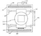
図1に本実施例で示すレーザー照射装置の断面の概要を示す。またその上面図を図2に示す。図1において、101はレーザー照射室である。レーザー照射室101は、外部から遮蔽され、減圧状態に保つことができる構成となっている。
【0019】
レーザー光は発振器102で発振され、光学系112により断面形状が線状に加工される。そしてミラー103で反射され、石英で構成された窓104を介して被処理基板301に照射される。
【0020】
レーザー発振装置102としては、XeClエキシマレーザー(波長308nm)を発振するものを用いる。他に、KrFエキシマレーザー(波長248nm)を用いることができる。
【0021】
被処理基板301は、台106上に設けられたステージ111上に配置され、台106内に設置されたヒーターによって、所定の温度(室温〜700℃)に保たれる。
【0022】
台106は、移動機構107によって、線状レーザー光の線方向に対して直角の方向に移動され、被処理基板301上面に対しレーザービームを走査しながら照射することを可能としている。
【0023】
レーザー照射室101は、真空排気ポンプ108を備えており、必要に応じて内部を減圧状態または真空状態にすることができる。
【0024】
またレーザー照射室101は、一対の電極109と気体供給部110を備えている。本実施例においては、一対の電極109はレーザー照射室101の側壁に沿って、基板を挟むように置かれている。一対の電極109は高周波電源113に接続されており、電極間にプラズマを発生可能としている。
【0025】
高周波電源113は、13.56 MHzの周波数の高周波を発振させる。高周波のパワーとしては200W〜2kW程度の範囲から選択すればよい。
【0026】
レーザー照射室101は、ゲイトバルブ401を有し、他の処理室との接続を可能なものとしている。また必要に応じて、ゲイトバルブ401を介して基板(試料)の出し入れを行うことができる構成となっている。
【0027】
図1及び図2に示す装置は、雰囲気を酸素または酸素を含有した減圧雰囲気とした状態で一対の電極109からの高周波放電によって酸素プラズマ雰囲気を形成し、この雰囲気の中で基板301上の半導体膜に対してレーザー光の照射を行うことができる。
【0028】
このような構成においては、酸素プラズマの作用によって半導体膜上の有機物が酸化除去され、膜中に有機物が混入することを防ぐことができる。
【0029】
〔実施例2〕
本実施例は、実施例1に示したレーザー照射装置を用いてガラス基板上に薄膜トランジスタを作製する場合の例を示す。
【0030】
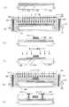
図3に、実施例の作製工程を示す。まず、被処理基板301として127mm角のコーニング1737ガラス基板を用意する。
【0031】
そして基板301上に下地膜としての酸化珪素膜302を2000Åの厚さに成膜する。成膜方法は、プラズマCVD法を用いる。次に図示しない非晶質珪素膜を500Åの厚さにプラズマCVD法により成膜する。
【0032】
次に10ppm程度の酢酸ニッケル水溶液をスピンコート法により、非晶質珪素膜上に塗布し、ニッケル元素が非晶質珪素膜の表面に接して保持された状態とする。このニッケルを用いた結晶化技術の詳細については、特開平6−244104号に記載されている。
【0033】
この状態において、600℃、4時間の加熱処理を水素含有雰囲気(即ち還元雰囲気)中で行う。この加熱処理により、非晶質珪素膜は結晶化し結晶性珪素膜303(図3(A))へと変成される。
【0034】
なお、最終的に膜中に残留するニッケル元素の濃度は、1×10¹⁵〜5×10¹⁹原子/cm3 の範囲内に収まることが望ましい。
【0035】
このようにして結晶性珪素膜303が得られる。次に得られた結晶性珪素膜303の結晶性をさらに高めるために、エキシマレーザーを用いてレーザーアニールを行う。
【0036】
レーザーアニールは図1に示す装置を用いて行う。レーザーアニールを行うに当たっては、雰囲気を純酸素100%(極力純度の高いものが好ましい)または適当な酸素濃度の雰囲気とし、その圧力は0.02〜0.03Torrとする。
【0037】
そして一対の電極109に、高周波電源113により高周波エネルギーを印加する。ここでは13.56MHzの高周波が400Wの出力で印加される。そして、一対の電極109間には酸素プラスマが形成される。
【0038】
また被処理基板301は、450℃の温度に加熱される。この状態において、非晶質珪素膜303の表面は、酸素プラズマ320に曝される。そして有機物が酸化除去される。また酸素プラズマの作用によって、その表面には極薄い酸化珪素膜304が形成される。この酸化珪素膜304の膜厚は10〜100Å程度である。この酸化珪素膜304は、不純物がほとんど混入されない、極めて良質な膜である。
【0039】
この状態でレーザー光の照射を行う。照射される線状レーザー光は、照射面上で幅0.34mm×長さ135mmの大きさを有する。エネルギー密度は100mJ/cm2 〜500mJ/cm2 、例えば260mJ/cm2 とする。
【0040】
このレーザー光の照射は、図1の台106を2.5mm/sで一方向に移動させながら行う。こうすることで、線状レーザー光を走査させながら被照射面に照射することができる。
【0041】
レーザーの発振周波数は200Hzとする。上記の条件でレーザー光の照射を行うと、照射面の一点において10〜50ショットのレーザー光が照射されることになる。
【0042】
上記の工程においては、酸素プラズマの作用によって、結晶性珪素膜の表面に付着していた有機物を除去した状態でレーザー光の照射を行うことができる。
【0043】
即ち、結晶性珪素膜に付着していた有機物は酸素プラズマの衝撃により分離され、揮発性酸化物となって除去された状態でレーザー光の照射を行うことができる。
【0044】
図1または図3(B)に示す一対の電極109は、レーザー照射室101の内壁側面に沿って、側壁とほぼ同じ大きさで設けられている。
【0045】
そしてこの一対の電極109により、レーザー照射室101内部全体にプラズマが形成される。従って、レーザー光の照射によって被処理基板から飛翔した有機物がレーザー照射室101の内壁や窓104の内側に付着しても、この付着物は酸素プラズマによってレーザーアニール工程中に除去される。すなわちレーザーアニールと同時にレーザー照射室101内のクリーニングが同時に行われる。
【0046】
また酸化珪素膜304は極めて薄いため、複数回のパルスレーザー照射によりほとんどが飛散してしまう。飛散した後に、酸素プラズマにより新たに極薄い酸化珪素膜が形成されることもある。
【0047】
またこの酸化珪素膜304の形成に際しては、その膜中に珪素膜の表面に残存している有機物が取り込まれた状態となる。従って、レーザー光の照射によって酸化珪素膜が飛散してしまうことにより、有機物が珪素膜中に取り込まれることを抑制することができる。
【0048】
また、酸素プラズマの作用によって形成される極薄い酸化膜は、レーザー光の照射時に膜の内部から水素等が噴出して、膜の表面に凹凸が形成されてしまうことを防ぐ役割も有している。
【0049】
レーザーアニールの終了後は、結晶性珪素膜303上面に酸化珪素膜が残ったり形成されたりし易い。そこで次の工程に移る前に、HF水溶液やHFとH2 O2 の混合水溶液で、結晶性珪素膜303の上面を還元させ、酸化珪素膜を除去することは好ましい。
【0050】
このようにして結晶性珪素膜303に対し、レーザーアニールが施され、その結晶性が向上される。(図3(B))
【0051】
作製された結晶性珪素膜303は、結晶性、膜質の均質性、また移動度等の電気的特性いずれも優れたものとすることができる。
【0052】
次に、レーザーアニールによってその結晶性が助長された結晶性珪素膜303を用いて薄膜トランジスタ(TFT)を作製する。まず結晶性珪素膜303をエッチングして、島状領域305を形成する。この島状領域305は後に薄膜トランジスタの活性層を構成することとなる。
【0053】
次に、ゲイト絶縁膜306となる酸化珪素膜をプラズマCVD法によって厚さ1200Åの厚さに成膜する。ここではこの酸化珪素膜を成膜するための原料ガスとして、TEOSおよび酸素を用いる。(図3(C))
【0054】
次に、ゲイト電極を作製する。ここではまず図示しないアルミニウム膜をスパッタ法により、6000Åの厚さに成膜する。なおアルミニウム膜中にスカンジウムまたは珪素を0.1〜2重量%含有させる。そしてこのアルミニウム膜をエッチングして、ゲイト電極307を形成する。(図3(C))
【0055】
次にソース/ドレイン領域を形成するための不純物イオンの注入を行う。ここではNチャネル型のTFTを作製するためにP(リン)イオンの注入をイオンドーピング法によって行う。
【0056】
このリンイオンの注入は、ゲイト電極307をマスクとして行われる。ドーピング条件は、ドーピングガスとして、フォスフィン(PH3 )を用い、加速電圧を80kV、ドーズ量を1×10¹⁵原子/cm2 として行う。また基板温度は室温とする。
【0057】
このドーピング工程においては、自己整合的にチャネル形成領域310と、N型の不純物領域であるソース領域308、さらにドレイン領域309が形成される。
【0058】
次に、ドーピングされた不純物を活性化するために、再び図1に示すレーザーアニール装置を用いて、線状レーザー光によりレーザーアニールを行う。ここで前記した条件で酸素プラズマを形成させて、酸素プラズマ雰囲気中でレーザーアニールを行う。(図3(E))
【0059】
照射面におけるレーザー光のエネルギー密度は、100mJ/cm2 〜350mJ/cm2 の範囲で行う。ここでは160mJ/cm2 とする。
【0060】
前述したように線状レーザービームを走査させながら照射を行う。このようにして被照射物の一点において20〜40ショットのレーザービームが照射されるようにする。
【0061】
このレーザーアニールにより、不純物が活性化されると共に、先の不純物イオンの注入時における損傷がアニールされる。このレーザーアニールの終了後、窒素雰囲気中にて2時間、450℃の熱アニールを行う。(図3(E))
【0062】
次に層間絶縁膜311として酸化珪素膜をプラズマCVD法で6000Åの厚さに成膜する。
【0063】
さらに層間絶縁膜311にコンタクトホールを形成し、金属材料、例えば、チタンとアルミニウムの多層膜でもってソース電極312とドレイン電極313を形成する。
【0064】
最後に、1気圧の水素雰囲気で、200〜350℃の熱アニール処理を行い図3(F)に示す薄膜トランジスタを完成させる。
【0065】
このようにして、複数のNおよび/またはPチャネル型の結晶性TFTが形成される。これらのTFTは、Nチャネル型で70〜120cm2 /Vs、Pチャネル型で60〜90cm2 /Vsの移動度を有する優れたものとすることができる。(図3(F))
【0066】
〔比較例〕
ここでは、実施例1に示すような酸素プラズマ雰囲気中でのレーザーアニールによってその結晶性が助長された結晶性珪素膜と、他の条件により得られた結晶性珪素膜との膜質を比較を示す。
【0067】
まず、酸素プラズマ雰囲気中ではなく、他の雰囲気中でレーザー光の照射を行った場合の例を示す。ここでは、
(A)空気
(B)酸素:窒素=20%:80%
(C)窒素100%
の3種類の雰囲気中でレーザー光の照射を行った場合の例を示す。
【0068】
なお雰囲気は大気圧とし、雰囲気以外の条件は実施例1と同じものとする。また上記比較条件においては、高周波放電は行わずにレーザーアニールを行った。
【0069】
空気雰囲気中で作製された結晶性珪素膜は、酸素プラズマ雰囲気中で形成されたものに比べてやや低い結晶性を有する。また、結晶性が不均一なものとなる傾向が見られる。また、移動度が低く、しかも膜面内において移動度のバラツキが大きい。さらに、複数毎の基板を処理した場合、基板毎の膜特性のバラツキが大きい。
【0070】
これらの原因は、基板表面の有機物が十分に除去されず、また空気中の不純物が膜中に混入するためと思われる。
【0071】
酸素:窒素=20%:80%雰囲気では、空気雰囲気中に比較して、移動度は向上するものの、結晶性の低い領域が点在するのとなってしまう。
【0072】
また窒素100%雰囲気では、膜全体の結晶性が低い。また移動度や膜質の面内均質性も低いものとなってしまう。
【0073】
また酸素プラズマ雰囲気中および酸素/窒素雰囲気で形成された結晶性珪素膜は、他の雰囲気で作製されたものに比較して、同一エネルギー密度では高い結晶性が得られる。
【0074】
特に酸素プラズマ雰囲気を利用したものは、他の比較例に比べて膜質が高く、また工程の再現性も高いものとすることができる。
【0075】
〔実施例3〕
本実施例は、実施例1に示すレーザー照射装置をマルチチャンバー方式の装置へと発展させた構成を示す。
【0076】
図4に、本実施例におけるレーザーアニール装置の上面図を示す。ここでは、図4に示すマルチチャンバー型のレーザーアニール装置を用いる。図4におけるA−A’断面を示す図が図1に相当する。
【0077】
図4に示す装置は、ロード/アンロード室406とレーザー照射室101と予備加熱室408と徐冷室410とが、基板搬送室402を介して接続された構成となっている。
【0078】
各室は気密性を有しており、必要とする雰囲気や圧力にすることができる。また各室は、ゲイトバルブ401、411、409、401によって基板搬送室402と連結されている。
【0079】
図4に示す装置において、406はロード/アンロード室であり、処理せんとする基板(試料)の出し入れが行われる室である。処理せんとする基板は、ロード/アンロード室406に多数枚(例えば20枚)が収納されたカセット毎搬入される。
【0080】
カセット毎搬入された基板は、基板搬送室402内に配置されたロボットアーム405により、一枚づつアライメント室403に移送される。
【0081】
アライメント室403には、被処理基板404とロボットアーム405との位置関係を修正するための、アライメント機構が配置されている。アライメント室403は、ロード/アンロード室406とゲイトバルブ407を介して接続されている。
【0082】
アライメント室403において位置調整がなされた基板404は、ロボットアーム405によって予備加熱室408に移送される。移送後はゲイトバルブ409を閉鎖し気密性を維持させる。なお、装置の動作中は全ての室を同じ圧力とし、各室間における基板の移送に際して圧力調整をしないで済むようにすることが望ましい。
【0083】
予備加熱室408においては、レーザーアニールされる基板を所定の温度まで予備的に加熱する。これはレーザー照射室101において基板加熱に要する時間を短縮させ、スループットの向上を図るためである。
【0084】
また、予備的に加熱させることで膜中の水素を離脱させ、レーザー光の照射による効果を高めるためでもある。この水素を離脱させる効果はアニールする膜として非晶質珪素膜を用いる場合に顕著なものとなる。
【0085】
予備加熱室408は、その内部が円筒状の石英で構成されている。円筒状の石英はヒーターで囲まれていて、その内部を加熱できる構成となっている。
【0086】
また予備加熱室408は、石英で構成された基板ホルダーを備えている。基板ホルダーには、基板が多数枚収容可能なサセプターが備えられている。基板ホルダーは、エレベーターにより上下される。また予備加熱室408と、基板搬送室402とは、ゲイトバルブ409によって連結されている。
【0087】
予備加熱室408において、所定の時間予熱された基板は、ロボットアーム405によって基板搬送室402に引き戻され、アライメント室403にて再度アライメント調整がなされる。そしてロボットアーム405によって、レーザー照射室101に移送される。
【0088】
レーザー照射終了後、被処理基板404はロボットアーム405によって基板搬送室402に引き出され、徐冷室410に移送される。
【0089】
徐冷室410は、ゲイトバルブ411を介して、基板搬送室402と接続されており、石英製のステージ上に配置された被処理基板が、ランプ、反射板からの赤外光を浴びて、徐々に冷却される。
【0090】
徐冷室410で徐冷された被処理基板は、ロボットアーム405によって、ロード/アンロード室406に移送され、カセット412に収納される。
【0091】
こうして、1枚の基板に対するレーザーアニール工程が実施される。このようにして、上記工程を繰り返すことにより、多数の基板に対して、連続的に一枚づつ処理が行われる。
【0092】
〔実施例4〕
本実施例は、非晶質珪素膜に対してレーザーアニールを施し、結晶性珪素膜を得る構成に関する。本実施例においても実施例1と同様に、図1に示すレーザー照射装置を用いる。
【0093】
まず、基板として127mm角、1.1mm厚のコーニング1737基板を用意する。この基板上にプラズマCVD法により酸化珪素膜を2000Åの厚さに形成し、下地膜とする。
【0094】
さらに公知のプラズマCVD法で非晶質珪素膜を500Åの厚さに形成する。その後、この基板をレーザー照射室101(図1)内に配置する。
【0095】
基板が置かれたレーザー照射室101に対して、気体供給部110から酸素を導入して照射室内の圧力を0.02〜0.03Torrに保つ。そして一対の電極109に、高周波電源113から高周波エネルギー(13.56 MHz)を400Wの出力で印加する。なお基板に加熱温度は450℃とする。
【0096】
すると、基板上の非晶質珪素膜は、その表面が酸化され、10〜100Åの酸化珪素膜が形成される。
【0097】
同時に、基板表面に付着した有機物は衝撃により分離され、揮発性酸化物となって除去される。または、この酸化膜中に残存した有機物が取り込まれる。
【0098】
酸素プラズマを発生させた状態で、台106を移動させながら、線状レーザー光を非晶質珪素膜に照射する。
【0099】
線状レーザー光は、照射面上で、幅0.34mm×長さ135mmの大きさを有する。エネルギー密度は、100mJ/cm2 〜400mJ/cm2 、例えば200mJ/cm2 とする。台106を2.5mm/sで一方向に移動させながら行うことで、線状レーザー光を走査させる。レーザーの発振周波数は200Hzとする。
【0100】
この場合、照射面の一点に注目すると、10〜50ショットのレーザー光が照射される。
【0101】
このようにして、酸素プラスマ雰囲気中で線状レーザー光を走査して照射することにより、非晶質珪素膜は結晶化され、結晶性珪素膜となる。
【0102】
作製された結晶性珪素膜は、清浄な膜質を有し、かつ、結晶性、膜の均質性に優れたものとすることができる。
【0103】
〔実施例5〕
本実施例は、実施例1に示す装置とは異なる電極の配置をした構成に関する。図5に本実施例の構成を示す。また、図6に図5の上面図を示す。なお図5及び図6において、図1および図2と同一部分を表示する場合には同符号を用いている。
【0104】
図5、6に示すように、本実施例においては一対の電極が基板に平行になるように配置されている。即ち、一対の電極の一方501は、被処理基板301の上方に存在し、他方の対向電極502は基板の下方に位置している。
【0105】
ミラー103で反射されたレーザー光は、電極501に設けられたスリットを介して照射される。なお、動作の方法については、実施例1に示したものと同じである。
【0106】
〔実施例6〕
本実施例は、実施例1に示す構成をさらに改良し、レーザーアニールが施される被照射面に対して効果的に酸素プラズマを供給する構成に関する。
【0107】
図7に本実施例で示すレーザー照射装置の横断面図を示す。図8には図7の上面図を示す。図7、図8において、図1および図2と同一部分を表示する場合には同符号を用いている。
【0108】
本実施例で示すプラズマを発生するための一対の電極701は、線状レーザー光に対して平行、かつ線状レーザー光が電極間を通過するように設けられている。この構成により酸素プラズマは、被処理基板上のレーザー光照射位置702の近傍にのみ形成される。
【0109】
この場合、一対の電極701の間隔と台106の移動速度で、被処理基板がプラズマに曝される時間を制御できる。
【0110】
このような構成とした場合、レーザー処理の最中において、同時にチャンバー内の洗浄を行うという効果は低いものとなる。しかし、レーザー光が照射される領域およびその近傍において効果的に酸素プラズマを発生させることができるので、被照射面の有機物を除去するという効果は最大限得ることができる。
【0111】
〔実施例7〕
これまでの実施例においては、レーザー光の照射を、被処理基板が酸素プラズマに曝されている状態で行った例を示した。他方、被処理基板を酸素プラズマに曝す工程を実施したあとにレーザー光の照射を行ってもよい。
【0112】
例えば、レーザー照射室において、まず被処理基板を酸素プラズマに十分に曝す。その後、プラズマの発生を停止し、レーザーアニールを行う。
【0113】
この場合、被処理面に有機物が付着しないような清浄な雰囲気または高真空な雰囲気を維持する必要がある。
【0114】
また、プラズマ処理室を設けて、この中で被処理基板を所定の時間酸素プラスマに曝し、その後、清浄な雰囲気を維持したまま被処理基板をレーザー照射室に搬送してレーザー照射を行ってもよい。
【0115】
酸素プラズマに曝す工程を、レーザー照射とは別の容器内で行う場合、被処理基板を外気に曝さないようにし、清浄な浄囲気を維持する機能が必要となる。
【0116】
例えば、プラズマ処理室とレーザー照射室とを、ゲイトバルブを介して接続する、いわゆるマルチチャンバー構成とする必要がある。
【0117】
この場合、レーザー照射時の雰囲気を水素または水素を含有した雰囲気とすると、水素熱処理も同時に行うことができる。またこの場合は、基板を300〜600℃程度に加熱することが重要となる。
【0118】
〔実施例8〕
本実施例では、被処理基板の被照射部を酸素プラズマに曝し、その後にレーザー光の照射を行う構成を示す。
【0119】
図9に本実施例で示す装置の断面図を示す。また図10に上面図を示す。図9、図10において、図1および図2と同一部分を表示する場合には同符号を用いている。
【0120】
図9、図10に示すように、一対の電極901は、レーザー光が走査されて照射される位置の手前側に配置されている。即ち、一対の電極901間を通過した領域にレーザー光が照射される構成となっている。
【0121】
このような構成とすると、まず一対の電極901間で生じるプラズマに曝された領域に対して、その後にレーザー光が照射されるものとすることができる。
【0122】
この場合、一対の電極901の間隔と台106の移動速度で、被処理基板がプラズマに曝される時間を制御することができる。
【0123】
〔実施例9〕
本実施例は、より高い密度で酸素プラズマを発生させる構成に関する。図11に本実施例で示すレーザー照射装置の断面図を示す。また図12にその上面図を示す。なお図1および図2と同一部分を表示する場合には同符号を用いている。
【0124】
本実施例においては、1101〜1104で示される4つの電極によって、処理室101内に高密度プラズマを生成させる構成となっている。
【0125】
本実施例においては、高周波発振器113から供給される高周波電力が、位相制御回路1105〜1108を通過することによって、それぞれその位相が制御される。そして、各電極から個々に位相が制御された高周波電力が処理室101内にそれぞれの電極から供給される。
【0126】
例えば、処理室101内においてリサージュ波形が描かれるように各電極に供給される高周波電力の位相を制御することで、生成される酸素プラズマの密度を高めることができる。
【0127】
〔実施例10〕
本実施例は、実施例1に示す構成において、レーザー処理室101内の雰囲気を酸素と水素との混合雰囲気とすることを特徴とする。
【0128】
酸素プラズマと水素プラズマとは、それぞれ有機物に対する除去作用を有している。2つのプラズマが除去作用をする対象は、異なる炭素の結合を有した有機物である。
【0129】
従って、酸素と水素の混合雰囲気においてプラズマを生成させることにより、珪素膜の表面に存在する有機物の除去をより効果的に行うことができる。
【0130】
また、レーザー光の照射の際に300℃〜600℃程度の加熱を行うことで、レーザー光の照射によるアニール効果を得るとともに、水素プラズマによる水素熱処理も同時に行うことができる。これは、珪素膜の表面及び膜中に存在する欠陥や不対結合手を補償するという顕著な効果を有している。
【0131】
また本実施例においては、酸素のプラズマも生成されるので、レーザー光の照射時に酸化膜が保護膜として形成されるという効果も同時に得ることができる。
【0132】
なお、酸素と水素の他に適当な希釈ガス、例えばヘリウム等を加えてもよい。また酸素と水素の混合比は、必要とする効果が得られるように適時設定すればよい。
【0133】
【発明の効果】
レーザー光の照射による半導体膜に対するアニール工程において、酸素プラズマおよび/または水素プラズマによって被処理面の有機物を除去することにより、レーザー光の照射による効果を高めることができる。
【0134】
具体的には、不純物が膜中に混入することを防ぐことができ、得られる膜質の向上、工程の再現性の向上、といった効果を得ることができる。
【0135】
【図面の簡単な説明】
【図1】 実施例におけるレーザー照射室を示す図。
【図2】 図1の上面図。
【図3】 実施例の作製工程を示す図。
【図4】 実施例におけるレーザーアニール装置の上面図。
【図5】 レーザー照射装置の例の横断面図。
【図6】 図5の上面図。
【図7】 レーザー照射装置の例の横断面図。
【図8】 図7の上面図。
【図9】 レーザー照射装置の例の横断面図。
【図10】図9の上面図。
【図11】レーザー照射装置の例の横断面図。
【図12】図11の上面図。
【符号の説明】
101 レーザー照射室
102 レーザー発振装置
103 ミラー
104 窓
106 台
107 移動機構
108 真空排気ポンプ
109 一対の電極
110 気体供給部
111 ステージ
112 光学系
113 高周波発振器
301 基板
302 酸化珪素膜(下地膜)
303 結晶化珪素膜
304 酸化珪素膜
305 島状領域
306 ゲイト絶縁膜
307 ゲイト電極
308 ソース
309 ドレイン
310 チャネル形成領域
311 層間絶縁膜
312 ソース電極・配線
313 ドレイン電極・配線
320 酸素プラズマ
401 ゲイトバルブ
402 基板搬送室
403 アライメント室
404 基板
405 ロボットアーム
406 ロード/アンロード室
407 ゲイトバルブ
408 予備加熱室
409 ゲイトバルブ
410 徐冷室
411 ゲイトバルブ
412 カセット
501 電極
502 電極
701 一対の電極
702 レーザー光照射位置
901 一対の電極
902 レーザー光照射位置
1101〜1104 電極
1105〜1108 位相制御回路[0001]
BACKGROUND OF THE INVENTION
The invention disclosed in this specification relates to a method and an apparatus for performing laser irradiation for annealing a substrate to be processed. Further, the present invention relates to a method and an apparatus for performing crystallization of a semiconductor film by laser irradiation or promoting crystallization.
[0002]
[Prior art]
2. Description of the Related Art Conventionally, a technique for irradiating a semiconductor film such as a silicon film with laser light to promote crystallization or crystallization is known.
[0003]
For example, a technique is known in which an amorphous or crystalline silicon film is formed on a glass substrate by a plasma CVD method or the like, and is irradiated with laser light to transform it into a crystalline silicon film.
[0004]
[Problems to be solved by the invention]
When laser annealing is performed in a state where an organic substance is adhered to the surface of the semiconductor film for some reason, the organic substance or a component constituting the organic substance is mixed in the film, and the film quality is deteriorated.
[0005]
The characteristics of a semiconductor film change greatly when a very small amount of impurities are mixed therein. Therefore, if laser annealing is performed with organic matter attached, the crystallinity of the region to which the organic matter has been attached is deteriorated, desired film characteristics cannot be obtained, or the characteristics are not uniform within the film surface, etc. Problem arises.
[0006]
In order to solve this problem, various cleaning steps are performed before laser annealing. However, at present, sufficient effects cannot be obtained by cleaning.
[0007]
An object of the invention disclosed in this specification is to eliminate the influence of organic substances attached to the surface of a semiconductor film in a crystallization or annealing process by laser light irradiation on the semiconductor film.
[0008]
Specifically, in the process of transforming a semiconductor film into a crystalline silicon film by laser light irradiation, the crystallinity of the resulting film is hindered or affected by the influence of organic substances adhering to the surface of the semiconductor film. An object is to prevent the reproducibility from being hindered.
[0009]
[Means for Solving the Problems]
The invention disclosed in this specification is
Annealing is performed by laser light irradiation while the surface of the semiconductor film is treated with plasma.
[0010]
Other aspects of the invention are:
The surface of the semiconductor film is treated with oxygen plasma, and annealing is performed by irradiating the surface of the semiconductor film with laser light.
[0011]
Other aspects of the invention are:
The surface of the semiconductor film is treated with hydrogen plasma, and annealing is performed by irradiating the surface of the semiconductor film with laser light.
[0012]
As the laser light in the invention disclosed in this specification, a continuous wave laser, a pulse laser, or the like can be used. It is particularly preferable to use a pulsed laser. It is extremely preferable to use a pulsed laser such as an excimer laser for a semiconductor, particularly a non-single-crystal silicon film.
[0013]
As a means for generating plasma, it is preferable to use a method by supplying electromagnetic energy (generally high frequency energy). Moreover, as means for generating plasma, means capable of generating high-density plasma as much as possible is preferable.
[0014]
[Action]
By annealing the surface of the silicon film by laser light irradiation with oxygen plasma,
It is possible to obtain effects such as removal of organic substances on the surface of the silicon film and prevention of surface roughness due to the formation of an oxide film on the surface of the silicon film.
[0015]
Also, by annealing the surface of the silicon film by laser light irradiation with hydrogen plasma,
By combining the removal of organic substances and the heat treatment on the surface of the silicon film, it is possible to obtain effects such as defect compensation for the silicon film by hydrogen and compensation for unpaired bonds.
[0016]
Furthermore, the synergistic effect by said effect | action can be acquired by setting it as the mixed atmosphere of oxygen and hydrogen.
[0017]
【Example】
[Example 1]
In this embodiment, a laser irradiation apparatus capable of irradiation with laser light in an oxygen plasma atmosphere is described.
[0018]
FIG. 1 shows an outline of a cross section of the laser irradiation apparatus shown in this embodiment. A top view thereof is shown in FIG. In FIG. 1, 101 is a laser irradiation chamber. The
[0019]
The laser light is oscillated by the
[0020]
As the
[0021]
The
[0022]
The
[0023]
The
[0024]
The
[0025]
The high
[0026]
The
[0027]
In the apparatus shown in FIGS. 1 and 2, an oxygen plasma atmosphere is formed by high frequency discharge from a pair of
[0028]
In such a configuration, the organic substance on the semiconductor film is oxidized and removed by the action of oxygen plasma, and the organic substance can be prevented from being mixed into the film.
[0029]
[Example 2]
In this example, a thin film transistor is formed over a glass substrate using the laser irradiation apparatus described in Example 1.
[0030]
FIG. 3 shows a manufacturing process of the example. First, a 127 mm square Corning 1737 glass substrate is prepared as the
[0031]
Then, a
[0032]
Next, an aqueous nickel acetate solution of about 10 ppm is applied onto the amorphous silicon film by spin coating so that the nickel element is held in contact with the surface of the amorphous silicon film. Details of the crystallization technique using nickel are described in JP-A-6-244104.
[0033]
In this state, heat treatment at 600 ° C. for 4 hours is performed in a hydrogen-containing atmosphere (that is, a reducing atmosphere). By this heat treatment, the amorphous silicon film is crystallized and transformed into a crystalline silicon film 303 (FIG. 3A).
[0034]
Note that it is desirable that the concentration of nickel element finally remaining in the film be within the range of 1 × 10¹⁵ to 5 × 10¹⁹ atoms / cm3 .
[0035]
In this way, a
[0036]
Laser annealing is performed using the apparatus shown in FIG. In performing the laser annealing, the atmosphere is 100% pure oxygen (preferably having as high purity as possible) or an atmosphere having an appropriate oxygen concentration, and the pressure is 0.02 to 0.03 Torr.
[0037]
Then, high frequency energy is applied to the pair of
[0038]
The substrate to be processed 301 is heated to a temperature of 450 ° C. In this state, the surface of the
[0039]
In this state, laser light irradiation is performed. The irradiated linear laser beam has a size of 0.34 mm width × 135 mm length on the irradiation surface. Energy density100mJ / cm 2 ~500mJ / cm 2 , for example, to 260 mJ / cm2.
[0040]
This laser light irradiation is performed while moving the table 106 in FIG. 1 in one direction at 2.5 mm / s. By doing so, it is possible to irradiate the irradiated surface while scanning the linear laser beam.
[0041]
The oscillation frequency of the laser is 200 Hz. When laser light irradiation is performed under the above conditions, 10 to 50 shots of laser light are irradiated at one point on the irradiated surface.
[0042]
In the above step, laser light irradiation can be performed in a state where organic substances adhering to the surface of the crystalline silicon film are removed by the action of oxygen plasma.
[0043]
In other words, the organic matter adhering to the crystalline silicon film is separated by the impact of oxygen plasma and can be irradiated with laser light in a state of being removed as a volatile oxide.
[0044]
A pair of
[0045]
The pair of
[0046]
Further, since the
[0047]
Further, when the
[0048]
In addition, the ultra-thin oxide film formed by the action of oxygen plasma also has the role of preventing the formation of irregularities on the film surface due to hydrogen and the like being ejected from the inside of the film when irradiated with laser light. Yes.
[0049]
After the laser annealing, the silicon oxide film is likely to remain or be formed on the upper surface of the
[0050]
In this way, the
[0051]
The produced
[0052]
Next, a thin film transistor (TFT) is manufactured using the
[0053]
Next, a silicon oxide film to be the
[0054]
Next, a gate electrode is produced. Here, an aluminum film (not shown) is first formed to a thickness of 6000 mm by sputtering. The aluminum film contains scandium or silicon in an amount of 0.1 to 2% by weight. Then, this aluminum film is etched to form a
[0055]
Next, impurity ions are implanted to form source / drain regions. Here, in order to fabricate an N-channel TFT, P (phosphorus) ions are implanted by an ion doping method.
[0056]
This phosphorus ion implantation is performed using the
[0057]
In this doping process, a channel formation region 310, a
[0058]
Next, in order to activate the doped impurities, laser annealing is again performed with linear laser light using the laser annealing apparatus shown in FIG. Here, an oxygen plasma is formed under the above-described conditions, and laser annealing is performed in an oxygen plasma atmosphere. (Figure 3 (E))
[0059]
The energy density of the laser beam on the irradiated surface is in a range of100mJ / cm 2 ~350mJ / cm 2 . Here, it is set to 160 mJ / cm2 .
[0060]
As described above, irradiation is performed while scanning with a linear laser beam. In this way, a laser beam of 20 to 40 shots is irradiated at one point of the irradiated object.
[0061]
By this laser annealing, the impurities are activated and the damage during the previous implantation of impurity ions is annealed. After the laser annealing, thermal annealing is performed at 450 ° C. for 2 hours in a nitrogen atmosphere. (Figure 3 (E))
[0062]
Next, a silicon oxide film is formed as an
[0063]
Further, contact holes are formed in the
[0064]
Finally, thermal annealing is performed at 200 to 350 ° C. in a hydrogen atmosphere of 1 atm to complete the thin film transistor shown in FIG.
[0065]
In this way, a plurality of N and / or P channel type crystalline TFTs are formed. These TFTs can be excellent having a mobility of 70 to 120 cm2 / Vs for the N-channel type and 60 to 90 cm2 / Vs for the P-channel type. (Fig. 3 (F))
[0066]
[Comparative Example]
Here, the film quality of a crystalline silicon film whose crystallinity is promoted by laser annealing in an oxygen plasma atmosphere as shown in Example 1 and a crystalline silicon film obtained under other conditions will be compared. .
[0067]
First, an example in which laser light irradiation is performed in another atmosphere instead of an oxygen plasma atmosphere will be described. here,
(A) Air (B) Oxygen: Nitrogen = 20%: 80%
(C) Nitrogen 100%
An example in which laser light irradiation is performed in the three types of atmospheres shown in FIG.
[0068]
The atmosphere is atmospheric pressure, and the conditions other than the atmosphere are the same as those in Example 1. Under the above comparison conditions, laser annealing was performed without performing high-frequency discharge.
[0069]
A crystalline silicon film produced in an air atmosphere has slightly lower crystallinity than that formed in an oxygen plasma atmosphere. There is also a tendency for the crystallinity to be non-uniform. Further, the mobility is low, and the mobility variation is large in the film plane. Furthermore, when a plurality of substrates are processed, there is a large variation in film characteristics between the substrates.
[0070]
These causes seem to be because organic substances on the substrate surface are not sufficiently removed, and impurities in the air are mixed into the film.
[0071]
In an atmosphere of oxygen: nitrogen = 20%: 80%, mobility is improved as compared with that in an air atmosphere, but regions having low crystallinity are scattered.
[0072]
In the 100% nitrogen atmosphere, the crystallinity of the entire film is low. In addition, the in-plane uniformity of mobility and film quality will be low.
[0073]
In addition, a crystalline silicon film formed in an oxygen plasma atmosphere and an oxygen / nitrogen atmosphere has higher crystallinity at the same energy density as compared with those formed in other atmospheres.
[0074]
In particular, those using an oxygen plasma atmosphere can have higher film quality and higher process reproducibility than other comparative examples.
[0075]
Example 3
This embodiment shows a configuration in which the laser irradiation apparatus shown in Embodiment 1 is developed into a multi-chamber apparatus.
[0076]
FIG. 4 shows a top view of the laser annealing apparatus in the present embodiment. Here, a multi-chamber laser annealing apparatus shown in FIG. 4 is used. The figure which shows the AA 'cross section in FIG. 4 corresponds to FIG.
[0077]
The apparatus shown in FIG. 4 has a configuration in which a load / unload
[0078]
Each chamber is airtight and can be set to the required atmosphere and pressure. Each chamber is connected to the
[0079]
In the apparatus shown in FIG. 4, a load / unload
[0080]
The substrates loaded for each cassette are transferred to the
[0081]
An alignment mechanism for correcting the positional relationship between the substrate to be processed 404 and the
[0082]
The
[0083]
In the preheating
[0084]
Further, it is also for preliminarily heating to release hydrogen in the film and enhancing the effect of laser light irradiation. This effect of releasing hydrogen becomes remarkable when an amorphous silicon film is used as the film to be annealed.
[0085]
The preheating
[0086]
The preheating
[0087]
In the preheating
[0088]
After completion of laser irradiation, the substrate to be processed 404 is pulled out to the
[0089]
The
[0090]
The substrate to be processed that has been slowly cooled in the
[0091]
Thus, the laser annealing process is performed on one substrate. In this way, by repeating the above process, a number of substrates are processed one by one continuously.
[0092]
Example 4
This embodiment relates to a configuration in which a crystalline silicon film is obtained by performing laser annealing on an amorphous silicon film. Also in the present embodiment, the laser irradiation apparatus shown in FIG.
[0093]
First, a 127 mm square and 1.1 mm thick Corning 1737 substrate is prepared as a substrate. A silicon oxide film having a thickness of 2000 mm is formed on this substrate by plasma CVD to form a base film.
[0094]
Further, an amorphous silicon film is formed to a thickness of 500 mm by a known plasma CVD method. Thereafter, this substrate is placed in the laser irradiation chamber 101 (FIG. 1).
[0095]
Oxygen is introduced from the
[0096]
Then, the surface of the amorphous silicon film on the substrate is oxidized, and a silicon oxide film having a thickness of 10 to 100 mm is formed.
[0097]
At the same time, organic substances adhering to the substrate surface are separated by impact and removed as volatile oxides. Alternatively, the organic matter remaining in the oxide film is taken in.
[0098]
In a state where oxygen plasma is generated, the amorphous silicon film is irradiated with linear laser light while moving the
[0099]
The linear laser beam has a size of 0.34 mm width × 135 mm length on the irradiated surface. The energy density is 100 mJ / cm2 to 400 mJ / cm2 , for example, 200 mJ / cm2 . A linear laser beam is scanned by moving the
[0100]
In this case, if attention is paid to one point on the irradiated surface, 10 to 50 shots of laser light are irradiated.
[0101]
In this way, the amorphous silicon film is crystallized into a crystalline silicon film by scanning and irradiating linear laser light in an oxygen plasma atmosphere.
[0102]
The produced crystalline silicon film has a clean film quality and is excellent in crystallinity and film homogeneity.
[0103]
Example 5
The present embodiment relates to a configuration in which electrodes different from those of the apparatus shown in the first embodiment are arranged. FIG. 5 shows the configuration of this embodiment. FIG. 6 is a top view of FIG. 5 and 6, the same reference numerals are used when the same parts as those in FIGS. 1 and 2 are displayed.
[0104]
As shown in FIGS. 5 and 6, in this embodiment, the pair of electrodes are arranged in parallel to the substrate. That is, one of the pair of
[0105]
The laser beam reflected by the
[0106]
Example 6
The present embodiment relates to a configuration in which the structure shown in the first embodiment is further improved and oxygen plasma is effectively supplied to an irradiated surface to be laser-annealed.
[0107]
FIG. 7 shows a cross-sectional view of the laser irradiation apparatus shown in this embodiment. FIG. 8 shows a top view of FIG. 7 and 8, the same reference numerals are used when the same parts as those shown in FIGS. 1 and 2 are displayed.
[0108]
The pair of
[0109]
In this case, the time during which the substrate to be processed is exposed to plasma can be controlled by the distance between the pair of
[0110]
In such a configuration, the effect of simultaneously cleaning the chamber during laser processing is low. However, since oxygen plasma can be effectively generated in the region irradiated with the laser light and in the vicinity thereof, the effect of removing the organic matter on the irradiated surface can be maximized.
[0111]
Example 7
In the examples so far, the example in which the laser beam is irradiated while the substrate to be processed is exposed to oxygen plasma has been shown. On the other hand, laser light irradiation may be performed after performing the step of exposing the substrate to be processed to oxygen plasma.
[0112]
For example, in a laser irradiation chamber, first, the substrate to be processed is sufficiently exposed to oxygen plasma. Thereafter, plasma generation is stopped and laser annealing is performed.
[0113]
In this case, it is necessary to maintain a clean atmosphere or a high-vacuum atmosphere in which organic substances do not adhere to the surface to be processed.
[0114]
Also, a plasma processing chamber may be provided, in which the substrate to be processed is exposed to oxygen plasma for a predetermined time, and then the substrate to be processed is transported to the laser irradiation chamber while performing a laser irradiation while maintaining a clean atmosphere. Good.
[0115]
In the case where the step of exposing to oxygen plasma is performed in a container different from the laser irradiation, it is necessary to have a function of maintaining a clean clean air so that the substrate to be processed is not exposed to the outside air.
[0116]
For example, it is necessary to adopt a so-called multi-chamber configuration in which a plasma processing chamber and a laser irradiation chamber are connected via a gate valve.
[0117]
In this case, if the atmosphere at the time of laser irradiation is an atmosphere containing hydrogen or hydrogen, hydrogen heat treatment can be performed simultaneously. In this case, it is important to heat the substrate to about 300 to 600 ° C.
[0118]
Example 8
In this embodiment, a configuration is shown in which an irradiated portion of a substrate to be processed is exposed to oxygen plasma, and then laser light irradiation is performed.
[0119]
FIG. 9 shows a cross-sectional view of the apparatus shown in this embodiment. FIG. 10 shows a top view. 9 and 10, the same reference numerals are used when the same parts as those in FIGS. 1 and 2 are displayed.
[0120]
As shown in FIGS. 9 and 10, the pair of
[0121]
With such a structure, first, a region exposed to plasma generated between the pair of
[0122]
In this case, the time during which the substrate to be processed is exposed to plasma can be controlled by the distance between the pair of
[0123]
Example 9
This embodiment relates to a configuration for generating oxygen plasma at a higher density. FIG. 11 shows a cross-sectional view of the laser irradiation apparatus shown in this embodiment. FIG. 12 is a top view thereof. In addition, when displaying the same part as FIG. 1 and FIG. 2, the same code | symbol is used.
[0124]
In this embodiment, high-density plasma is generated in the
[0125]
In the present embodiment, the phase of the high frequency power supplied from the
[0126]
For example, the density of the generated oxygen plasma can be increased by controlling the phase of the high-frequency power supplied to each electrode so that a Lissajous waveform is drawn in the
[0127]
Example 10
This embodiment is characterized in that, in the configuration shown in Embodiment 1, the atmosphere in the
[0128]
Oxygen plasma and hydrogen plasma each have an action of removing organic substances. The object to which the two plasmas are removed is an organic substance having different carbon bonds.
[0129]
Therefore, by generating plasma in a mixed atmosphere of oxygen and hydrogen, organic substances present on the surface of the silicon film can be more effectively removed.
[0130]
Further, by performing heating at about 300 ° C. to 600 ° C. at the time of laser light irradiation, an annealing effect by laser light irradiation can be obtained, and hydrogen heat treatment by hydrogen plasma can be performed simultaneously. This has a remarkable effect of compensating for defects and dangling bonds existing on the surface of the silicon film and in the film.
[0131]
In the present embodiment, oxygen plasma is also generated, so that an effect that an oxide film is formed as a protective film at the time of laser light irradiation can be obtained at the same time.
[0132]
In addition to oxygen and hydrogen, an appropriate diluent gas such as helium may be added. Further, the mixing ratio of oxygen and hydrogen may be set in a timely manner so as to obtain the required effect.
[0133]
【The invention's effect】
In the annealing step for the semiconductor film by laser light irradiation, the organic substance on the surface to be processed is removed by oxygen plasma and / or hydrogen plasma, whereby the effect of laser light irradiation can be enhanced.
[0134]
Specifically, it is possible to prevent impurities from being mixed into the film, and to obtain effects such as improvement of the obtained film quality and improvement of process reproducibility.
[0135]
[Brief description of the drawings]
FIG. 1 is a diagram showing a laser irradiation chamber in an embodiment.
FIG. 2 is a top view of FIG.
FIG. 3 is a diagram showing a manufacturing process of the example.
FIG. 4 is a top view of a laser annealing apparatus in an embodiment.
FIG. 5 is a cross-sectional view of an example of a laser irradiation apparatus.
6 is a top view of FIG. 5;
FIG. 7 is a cross-sectional view of an example of a laser irradiation apparatus.
FIG. 8 is a top view of FIG.
FIG. 9 is a cross-sectional view of an example of a laser irradiation apparatus.
10 is a top view of FIG. 9;
FIG. 11 is a cross-sectional view of an example of a laser irradiation apparatus.
12 is a top view of FIG. 11. FIG.
[Explanation of symbols]
DESCRIPTION OF
303
Claims (13)
Translated fromJapanese前記酸素プラズマ処理によって前記非晶質珪素膜の表面に付着する有機物が除去され、同時に前記非晶質珪素膜上に酸化膜が形成されることを特徴とする結晶性珪素膜作製方法。Irradiating the surface of the amorphous silicon film with laser light simultaneously with the oxygen plasma treatment on the surface of the amorphous silicon film,
A method forproducing acrystalline silicon film , wherein organic substancesadhering tothe surfaceof theamorphous silicon film are removed by the oxygen plasma treatment, and at the same time, an oxide film is formed on theamorphous silicon film.
前記水素プラズマ処理によって前記非晶質珪素膜の表面に付着する有機物が除去され、同時に前記非晶質珪素膜の欠陥や不対結合手が補償されることを特徴とする結晶性珪素膜作製方法。Irradiating the surface of the amorphous silicon film with laser light simultaneously with the oxygen plasma treatment and the hydrogen plasma treatment on the surface of the amorphous silicon film,
A method forproducing acrystallinesilicon film,wherein organic matteradhering tothe surfaceof theamorphous silicon film is removed by the hydrogen plasma treatment, and at the same time, defects and dangling bonds of theamorphous silicon film are compensated. .
前記水素プラズマ処理によって前記非晶質珪素膜の表面に付着する有機物が除去されることを特徴とする結晶性珪素膜作製方法。The surface of the amorphous silicon film is subjected to oxygen plasma treatment and hydrogen plasma treatment by irradiating the surface of the amorphous silicon film with laser light while heating in a plasma containing oxygen and hydrogen. At the same time, irradiate the laser beam,
Crystalline silicon film manufacturing method characterized in that the organic substance attached is removed to the surface ofthe amorphous silicon film bythe waterMotopu plasmaprocessing.
前記水素プラズマ処理によって前記非晶質珪素膜の表面に付着する有機物が除去され、Organic matter adhering to the surface of the amorphous silicon film is removed by the hydrogen plasma treatment,
前記酸素プラズマ処理によって前記非晶質珪素膜の表面に付着する有機物が除去され、同時に前記非晶質珪素膜上に酸化膜が形成されることを特徴とする結晶性珪素膜作製方法。A method for producing a crystalline silicon film, wherein organic substances adhering to the surface of the amorphous silicon film are removed by the oxygen plasma treatment, and at the same time, an oxide film is formed on the amorphous silicon film.
前記プラズマを発生させる手段により酸素を含有した雰囲気においてプラズマが発生され、前記非晶質珪素膜の表面を処理するとともに前記レーザー光を照射する手段により前記非晶質珪素膜の表面にレーザー光が照射されることを特徴とするレーザー照射装置。A means for irradiating a laser beam to the amorphous silicon film, and means for generating anup plasma, the pressure can be reduced processing chamber having a
The plasma plasma in an atmosphere containing oxygen by means for generating is generated, the laserbeam on the surface of the amorphous siliconfilm by means of irradiating the laser beam as well as treating the surface of the amorphous silicon film A laserirradiation apparatus characterizedby beingirradiated .
前記プラズマを発生させる手段により酸素及び水素を含有した雰囲気においてプラズマが発生され、前記非晶質珪素膜の表面を処理するとともに前記非晶質珪素膜を300℃から600℃に加熱しながら前記レーザー光を照射する手段により前記非晶質珪素膜の表面にレーザー光が照射されることを特徴とするレーザー照射装置。A means for irradiating a laser beam to the amorphous silicon film, and means for generating anup plasma, the pressure can be reduced processing chamber having a
Plasma is generated in an atmosphere containing oxygen and hydrogen by the means for generating plasma, the surface of the amorphous silicon film is treated, and the laser is heated while heating the amorphous silicon film from 300 ° C. to 600 ° C. A laserirradiation apparatus, wherein the surface of the amorphous silicon filmis irradiated with laserlight by means of irradiating light.
Priority Applications (1)
| Application Number | Priority Date | Filing Date | Title |
|---|---|---|---|
| JP32822395AJP4001645B2 (en) | 1995-11-22 | 1995-11-22 | Crystalline silicon film manufacturing method and laser irradiation apparatus |
Applications Claiming Priority (1)
| Application Number | Priority Date | Filing Date | Title |
|---|---|---|---|
| JP32822395AJP4001645B2 (en) | 1995-11-22 | 1995-11-22 | Crystalline silicon film manufacturing method and laser irradiation apparatus |
Publications (2)
| Publication Number | Publication Date |
|---|---|
| JPH09148267A JPH09148267A (en) | 1997-06-06 |
| JP4001645B2true JP4001645B2 (en) | 2007-10-31 |
Family
ID=18207823
Family Applications (1)
| Application Number | Title | Priority Date | Filing Date |
|---|---|---|---|
| JP32822395AExpired - Fee RelatedJP4001645B2 (en) | 1995-11-22 | 1995-11-22 | Crystalline silicon film manufacturing method and laser irradiation apparatus |
Country Status (1)
| Country | Link |
|---|---|
| JP (1) | JP4001645B2 (en) |
Families Citing this family (4)
| Publication number | Priority date | Publication date | Assignee | Title |
|---|---|---|---|---|
| JPH1167663A (en)* | 1997-08-18 | 1999-03-09 | Fujitsu Ltd | Method for manufacturing semiconductor device |
| WO2002041363A2 (en)* | 2000-11-16 | 2002-05-23 | Solarflex Technologies, Inc. | System and methods for laser assisted deposition |
| WO2007046290A1 (en)* | 2005-10-18 | 2007-04-26 | Semiconductor Energy Laboratory Co., Ltd. | Semiconductor device and manufacturing method thereof |
| KR101610260B1 (en)* | 2008-12-15 | 2016-04-08 | 삼성전자주식회사 | Electron beam anneling apparatus and annealing method using the same |
- 1995
- 1995-11-22JPJP32822395Apatent/JP4001645B2/ennot_activeExpired - Fee Related
Also Published As
| Publication number | Publication date |
|---|---|
| JPH09148267A (en) | 1997-06-06 |
Similar Documents
| Publication | Publication Date | Title |
|---|---|---|
| KR100386202B1 (en) | Method for manufacturing a semiconductor device | |
| JP3165304B2 (en) | Semiconductor device manufacturing method and semiconductor processing apparatus | |
| KR100230485B1 (en) | Semiconductor processing system | |
| JP3161450B2 (en) | Substrate processing apparatus, gas supply method, and laser light supply method | |
| US20030132205A1 (en) | Laser processing method and laser processing apparatus | |
| JP2002100578A (en) | Thin film forming system | |
| JPH11307450A (en) | Reforming method of thin film and device used for its operation | |
| JP3977455B2 (en) | Method for manufacturing semiconductor device | |
| JP3927634B2 (en) | Laser annealing method and thin film transistor manufacturing method | |
| JP3165324B2 (en) | Method for manufacturing semiconductor device | |
| KR100320788B1 (en) | Laser irradiation method and semiconductor device manufacturing method | |
| JP4001647B2 (en) | Method for manufacturing crystalline semiconductor film | |
| JP3926862B2 (en) | Semiconductor processing method and thin film transistor manufacturing method | |
| JP4001645B2 (en) | Crystalline silicon film manufacturing method and laser irradiation apparatus | |
| JP3886554B2 (en) | Laser annealing method | |
| JPH07221035A (en) | Substrate treating device and its operation | |
| JP4036278B2 (en) | Ion doping equipment | |
| JP3621154B2 (en) | Method for manufacturing active matrix display device | |
| JP3859946B2 (en) | Method for manufacturing semiconductor device | |
| JP3763908B2 (en) | Laser irradiation system | |
| JP3612018B2 (en) | Method for manufacturing semiconductor device | |
| JPH09186342A (en) | Manufacture of semiconductor device | |
| JP4128552B2 (en) | Method for manufacturing semiconductor device | |
| JP3605326B2 (en) | Multi-chamber equipment | |
| JPH09139357A (en) | Method and apparatus for laser annealing |
Legal Events
| Date | Code | Title | Description |
|---|---|---|---|
| A977 | Report on retrieval | Free format text:JAPANESE INTERMEDIATE CODE: A971007 Effective date:20040430 | |
| A131 | Notification of reasons for refusal | Free format text:JAPANESE INTERMEDIATE CODE: A131 Effective date:20061031 | |
| A521 | Written amendment | Free format text:JAPANESE INTERMEDIATE CODE: A523 Effective date:20061228 | |
| TRDD | Decision of grant or rejection written | ||
| A01 | Written decision to grant a patent or to grant a registration (utility model) | Free format text:JAPANESE INTERMEDIATE CODE: A01 Effective date:20070814 | |
| A61 | First payment of annual fees (during grant procedure) | Free format text:JAPANESE INTERMEDIATE CODE: A61 Effective date:20070815 | |
| FPAY | Renewal fee payment (event date is renewal date of database) | Free format text:PAYMENT UNTIL: 20100824 Year of fee payment:3 | |
| R150 | Certificate of patent or registration of utility model | Free format text:JAPANESE INTERMEDIATE CODE: R150 | |
| FPAY | Renewal fee payment (event date is renewal date of database) | Free format text:PAYMENT UNTIL: 20100824 Year of fee payment:3 | |
| FPAY | Renewal fee payment (event date is renewal date of database) | Free format text:PAYMENT UNTIL: 20100824 Year of fee payment:3 | |
| FPAY | Renewal fee payment (event date is renewal date of database) | Free format text:PAYMENT UNTIL: 20110824 Year of fee payment:4 | |
| FPAY | Renewal fee payment (event date is renewal date of database) | Free format text:PAYMENT UNTIL: 20110824 Year of fee payment:4 | |
| FPAY | Renewal fee payment (event date is renewal date of database) | Free format text:PAYMENT UNTIL: 20120824 Year of fee payment:5 | |
| FPAY | Renewal fee payment (event date is renewal date of database) | Free format text:PAYMENT UNTIL: 20120824 Year of fee payment:5 | |
| FPAY | Renewal fee payment (event date is renewal date of database) | Free format text:PAYMENT UNTIL: 20130824 Year of fee payment:6 | |
| R250 | Receipt of annual fees | Free format text:JAPANESE INTERMEDIATE CODE: R250 | |
| R250 | Receipt of annual fees | Free format text:JAPANESE INTERMEDIATE CODE: R250 | |
| LAPS | Cancellation because of no payment of annual fees |