JP3999979B2 - Impact-resistant film for flat display panel and flat display panel - Google Patents
Impact-resistant film for flat display panel and flat display panelDownload PDFInfo
- Publication number
- JP3999979B2 JP3999979B2JP2002048157AJP2002048157AJP3999979B2JP 3999979 B2JP3999979 B2JP 3999979B2JP 2002048157 AJP2002048157 AJP 2002048157AJP 2002048157 AJP2002048157 AJP 2002048157AJP 3999979 B2JP3999979 B2JP 3999979B2
- Authority
- JP
- Japan
- Prior art keywords
- layer
- impact
- display panel
- flat display
- film
- Prior art date
- Legal status (The legal status is an assumption and is not a legal conclusion. Google has not performed a legal analysis and makes no representation as to the accuracy of the status listed.)
- Expired - Fee Related
Links
Images


Landscapes
- Shielding Devices Or Components To Electric Or Magnetic Fields (AREA)
- Devices For Indicating Variable Information By Combining Individual Elements (AREA)
- Optical Filters (AREA)
- Surface Treatment Of Optical Elements (AREA)
- Laminated Bodies (AREA)
Description
Translated fromJapanese【0001】
【発明の属する技術分野】
本発明は、平面型ディスプレイパネルの前面ガラスに取り付けられ、衝撃による前面ガラスの破砕を防止するとともに、軽量化及び薄型化を可能にした平面型ディスプレイパネル用耐衝撃フィルム及びそれを用いた平面型ディスプレイパネルに関する。
【0002】
【従来の技術】
近年、大画面パネルを作製でき、明瞭なフルカラー表示が可能であるなどの利点を有するプラズマディスプレイパネル(以下、PDPと略記する。)が注目されている。PDPは、2枚のガラス板間に隔離形成された多数の放電セル内で蛍光体を選択的に放電発光させることでフルカラー表示を行うものである。
【0003】
図1は、PDPの構造を例示する図であり、この図中符号1で示すPDPは、前面ガラス2と背面ガラス3とが対向配置された構成になっており、双方のガラス2,3間の隙間には減圧状態でキセノン等の希ガスが封入されている。前面ガラス2には放電電極4、誘電体膜5、保護膜6等が形成され、背面ガラス3には隔壁7、蛍光体8A,8B,8C、アドレス電極9等が設けられている。
PDP1の前面ガラス2は、電極や各種材料からなる薄膜等を積層形成する際、傷や歪みを受けており、元のガラス板に比べて強度が著しく低下している。さらに、背面ガラスに形成された隔壁や蛍光体の凹凸が接することで、それらの接触部分に応力集中が生じ易くなっている。
【0004】
従来、PDP等の平面型ディスプレイパネルの前面ガラス破損を防止するために、前面ガラスの前方に数ミリの間隔をおいて、アクリル樹脂や強化ガラス等からなる保護板を設け、平面型ディスプレイパネルに衝撃が加わることを防止していた。しかし、このような保護構造は、平面型ディスプレイパネルの軽量化、薄型化の妨げとなる問題があった。さらに、パネルの前面ガラスと保護板との間に空間があるため、蛍光灯等の外光の映り込みによる画質低下を生じたり、僅かな振動により画像の歪みを生じるといった問題があった。
【0005】
平面型ディスプレイパネルの前面ガラス破損を防止するための技術は、これまでに種々提案されており、例えば特開2000−123751号公報には、前面ガラスの厚みを厚くすることで強度を向上させる技術が提案されている。しかしこの構造では衝撃に対する保護効果は不十分であり、またパネル重量が増加することから問題である。
また、特開2000−156182号公報、特開平11−119667号公報、特開平11−119668号公報、特開平11−119669号公報においては、保護板を接着層を介してパネルの前面ガラスに接着する構造が提案されているが、この構造では衝撃が前面ガラスに伝わり易く、前面ガラスの破損防止効果が充分に得られない問題があった。
【0006】
さらに別な従来技術として、特開2001−266759号公報には、平面型ディスプレイパネルの前面ガラスに透明な粘着剤層を介して、割れ防止層(衝撃緩和層)Bとその上の飛散防止層Aとの順に透明な合成樹脂からなる2つの層を積層し、飛散防止層Aのせん断弾性率が2×10⁸Pa以上であり、割れ防止層Bのせん断弾性率が1×10⁴〜2×10⁸Paの範囲内である衝撃緩和積層体(以下、従来積層体という。)が提案されている。
【0007】
【発明が解決しようとする課題】
しかしながら、上記従来積層体は、PDPなどの前面ガラスにおける耐衝撃性付与という点では不十分であった。同公報の実施例においては、ガラス板として、電極や各種材料からなる薄膜等を積層形成していない、いわば「無処理」のガラス板を使用し、これに粘着剤、衝撃緩和層、飛散防止層を順に積層して硬球を落下させ、耐衝撃性の有無を試験しているが、上述した通り、実際のPDPの前面ガラスは、電極や各種材料からなる薄膜等を積層形成した結果、無処理のガラスに比べて耐衝撃力が大幅に劣化し、割れやすくなっている。このように従来積層体は、耐衝撃力が無処理のガラス板に比べて大幅に弱化しているPDPの前面ガラスに接合した場合、十分な耐衝撃効果が得られることは実証されていない。そして後述する実施例において詳述するが、ガラス板に電極や誘電体膜などを形成しPDPの前面ガラスを想定したガラス基板に、同公報の実施例中に記載されたものと同等の材質と厚みの三層を積層し、スプリングインパクトハンマーにより所定の衝撃力を加えて耐衝撃性を測定したところ、このものは耐衝撃性が不足していることが判った(実施例の例8参照)。
従って従来積層体は、耐衝撃性が弱化しているPDPなど平面型ディスプレイパネルの前面ガラスを保護するための耐衝撃フィルムとしては不十分であった。
【0008】
本発明は、平面型ディスプレイパネルの前面に取り付けて、衝撃を受けた際にパネルのガラス破砕及び飛散を防止するとともに、軽量化及び薄型化が可能な平面型ディスプレイパネル用耐衝撃フィルム(以下、耐衝撃フィルムと略記する。)およびそれを用いた平面型ディスプレイパネルの提供を目的としている。
【0009】
【課題を解決するための手段】
上記目的を達成するために、本発明は、平面型ディスプレイパネル本体の前面ガラスに接合される耐衝撃フィルムであって、せん断弾性率が1×10³Pa〜1×10⁶Paの透明な合成樹脂からなり、平面型ディスプレイパネルの前面ガラス側の第1の層と、せん断弾性率が1×10⁸Pa以上の透明な合成樹脂からなり、該第1の層よりも視認側の第2の層と、せん断弾性率が1×10⁶Pa以上1×10⁸Pa未満の透明な合成樹脂からなり、該第2の層よりも視認側の第3の層とを含むことを特徴とする平面型ディスプレイパネル用耐衝撃フィルムを提供する。
本発明の耐衝撃フィルムは、せん断弾性率が1×10⁸Pa以上の硬質な合成樹脂からなる第2の層と平面型ディスプレイパネルの前面ガラスとの間に、せん断弾性率が1×10³Pa〜1×10⁶Paの軟質な合成樹脂からなる第1の層を設けるとともに、第2の層の視認側にせん断弾性率が1×10⁶Pa以上1×10⁸Pa未満の第3の層を積層した構成としたので、衝撃を受けた際、第3の層で衝撃力が分散、吸収され、さらに第2の層と前面ガラスの間に設けられた軟質な第1の層によって衝撃が吸収されて前面ガラスへの衝撃力の伝達が防止され、軽量、薄型で耐衝撃性の優れた耐衝撃フィルムを提供できる。
【0010】
本発明の耐衝撃フィルムにおいて、前記第1の層の視認側面に前記第2の層が積層された構造とするのが好ましい。
また前記第1の層は、前記平面型ディスプレイパネルの前面ガラスに直接接合される粘着性を有する樹脂材料が好ましい。
さらに、前記第1の層の厚みが1.0〜4.0mmの範囲であり、前記第2の層の厚みが0.05〜3.0mmであり、前記第3の層の厚みが0.05〜2.0mmであることが望ましい。
また、前記第2の層の視認側に、電磁波遮蔽層、近赤外線吸収層、反射防止層からなる群から選択される少なくとも1つの層と、これらの層間を接着する接着剤層とが積層された構成としてよい。
【0011】
さらに本発明は、上述した耐衝撃フィルムを、平面型ディスプレイパネル本体の前面ガラスに直接または透明接着剤層を介して接合してなる平面型ディスプレイパネルを提供する。
【0012】
【発明の実施の形態】
図2は本発明の耐衝撃フィルムの一実施例を示す図であって、この耐衝撃フィルム10は、動的粘弾性測定におけるせん断弾性率G´(以下、せん断弾性率と略記する。)が1×10³Pa〜1×10⁶Paの透明な合成樹脂からなり、平面型ディスプレイパネル本体11の前面ガラス12側に設けられた第1の層13と、せん断弾性率が1×10⁸Pa以上の透明な合成樹脂からなり、該第1の層13の視認側面に設けられた第2の層14と、せん断弾性率が1×10⁶Pa以上1×10⁸Pa未満の透明な合成樹脂からなり、該第2の層14の視認側面に積層された第3の層15とからなっている。
【0013】
上記せん断弾性率(G´)は、セイコーインスツルメンツ社製動的粘弾性測定装置DMS120を用い、周波数1Hzにおける25℃±3℃でのせん断弾性率G´の測定値である。なお一般的には引っ張り弾性率E=3G´(せん断弾性率)の関係があり、引っ張り弾性率Eは、上記せん断弾性率の約3倍程度である。
【0014】
[第1の層]
平面型ディスプレイパネル本体11の前面ガラス12側に設けられる第1の層13は、せん断弾性率が1×10³Pa〜1×10⁶Paの透明な合成樹脂からなる。このような合成樹脂は、ウレタン系樹脂、アクリル系樹脂、シリコーン系樹脂、フェノール樹脂、ユリア樹脂、エポキシ樹脂、フッ素樹脂、ビニル系樹脂、ブタジエン樹脂、ネオプレン樹脂、スチレン樹脂、アクリロニトリル樹脂等を単体または2種類以上の異なる樹脂をブレンド又は共重合したものなどから適宜選択して用いることができるが、耐衝撃性、破損ガラス飛散防止性、透明性、自己修復性、耐熱性、耐久性等のバランスを考慮すると、熱硬化性樹脂であるウレタン系樹脂およびシリコーン系樹脂が最も好ましい。このような熱硬化性樹脂を用いることによって、前面ガラス12が比較的高い温度にさらされるPDPに該耐衝撃フィルム10を適用した場合であっても、前面ガラス12に接する第1の層13が軟化、溶融流下するなどの不具合を生じることなく、長期にわたり優れた耐衝撃性を維持することができる。
【0015】
この第1の層13のせん断弾性率は、1×10³Pa〜1×10⁶Pa、好ましくは4×10³Pa〜6×10⁵Paとされる。せん断弾性率を上記範囲とすることによって、第2の層14側から前面ガラス12に向けて伝えられる衝撃力を効率よく分散および緩和吸収し、平面型ディスプレイパネル本体11の前面ガラス12の破壊を防止することができ、該破壊防止効果を高くできる。また、上記範囲のせん断弾性率の材料を選定することにより、第1の層13を積層する際の取り扱いが容易になるとともに、形状が安定した層を形成できる点でも有利である。
さらに、上記範囲のせん断弾性率を有する熱硬化性樹脂の中でも、粘着性を有するもの、例えばジェルテック社製のシリコーンフィルム、商品名αGEL、θ−5、θ−6、θ−7およびθ−8のような樹脂材料は、前面ガラス12の視認側面に配置し、その上に第2の層14を載せてゴムロール等を用いて押圧処理することによって簡単に前面ガラス12の視認側面に積層でき、製造工程が大幅に簡略化できることから好ましい。第1の層13の粘着性が十分でない場合には、透明な粘着剤層を第1の層13の両面に設けて前面ガラス12と第2の層14との接合を行うように構成することができる。
【0016】
第1の層13の厚みは1.0〜4.0mmが好ましく、1.5〜3.0mmがさらに好ましい。第1の層13が1.0mm以上あれば、上記衝撃力を効率よく分散および緩和することができ、4.0mm以下にすることで加工性に優れ、価格的に有利になることから好ましい。
【0017】
第1の層13中には、レベリング剤、脱泡剤、色調補正色素、近赤外線吸収(反射)色素、帯電防止剤、熱安定剤、酸化防止剤、分散剤、難燃剤、滑剤、可塑剤、または紫外線吸収剤等が含有されていてもよい。さらに、第1の層13と第2の層14との層間に、色調補正色素、近赤外線吸収(反射)色素、帯電防止剤、紫外線吸収剤等を含む層を介在させることもできる。
【0018】
上記第1の層13の材料としてウレタン系樹脂およびシリコーン系樹脂などの熱硬化型樹脂を用いる場合、適当な厚みの第1の層13を形成するには、浸漬コーティング法、スプレーコーティング法、スピンナーコーティング法、ビードコーティング法、ワイヤーバーコーティング法、ブレードコーティング法、ロールコーティング法、カーテンコーティング法、スリットダイコーター法、グラビアコーター法、スリットリバースコーター法、マイクログラビア法、またはコンマコーター法等のコーティング法、押し出し成型法、カレンダーロール成型法、バッチ成型法等を用いて製造することができる。加工性を向上させるため、トルエン、MEK、酢酸エチル、塩化メチレン、アルコール等の有機溶剤で上記熱硬化性樹脂を希釈して塗工することができる。第1の層13は、上記熱硬化性樹脂を適当な基板上に塗工して得られるフィルムを用いる他、前面ガラス12の視認側面または第2の層14の前面ガラス側面に直接塗工することもできる。
【0019】
[第2の層]
第2の層14は、せん断弾性率が1×10⁸Pa以上の透明な合成樹脂からなる。この第2の層14は、例えば、ポリエチレンテレフタレート、ポリエチレンナフタレート、ポリブチレンテレフタレート等のポリエステル樹脂、ジアセチルセルロース、トリアセチルセルロース、プロピオニルセルロース、ブチリルセルロース、ニトロセルロース等のセルロースエステル樹脂、ポリアミド樹脂、ポリカーボネート樹脂、ポリアリレート樹脂、ポリスチレン樹脂、エチレン−酢酸ビニル共重合体樹脂、ポリプロピレン、ポリメチルペンテン等のポリオレフィン樹脂、アクリル樹脂、ポリエーテルケトン樹脂、ポリウレタン樹脂、ポリエーテルイミド樹脂が挙げられ、特に耐衝撃性に優れたポリエステル樹脂およびポリカーボネート樹脂が好ましい。
【0020】
第2の層14の厚みは、0.05〜3.0mmが好ましく、0.1〜2.0mmがさらに好ましい。第2の層14の厚みを上記範囲とすることで、耐衝撃性を向上させることができるとともに、貼合時の作業性が向上する。また、この第2の層14のせん断弾性率を1×10⁸Pa以上、好ましくは2×10⁸Pa〜1×10¹⁰Paとすることで、第1の層13と積層した状態で耐衝撃性が十分な耐衝撃フィルムを構成することができる。第2の層14を基材として、その片面側に上記第1の層13を成膜する場合には、該第2の層14の表面にコロナ処理や易接着処理を施すことが好ましい。この第2の層14にレベリング剤、脱泡剤、色調補正色素、近赤外線吸収(反射)色素、帯電防止剤、熱安定剤、酸化防止剤、分散剤、難燃剤、滑剤、可塑剤、または紫外線吸収剤等が含有されていてもよい。
【0021】
[第3の層]
第3の層15は、せん断弾性率が1×10⁶Pa以上1×10⁸Pa未満の透明な合成樹脂からなる。この第3の層15は、例えば、ポリウレタン系樹脂、ポリエチレンテレフタレート、ポリエチレンナフタレート、ポリブチレンテレフタレート等のポリエステル樹脂、ジアセチルセルロース、トリアセチルセルロース、プロピオニルセルロース、ブチリルセルロース、ニトロセルロース等のセルロースエステル樹脂、ポリアミド樹脂、ポリカーボネート樹脂、ポリアリレート樹脂、ポリスチレン樹脂、エチレン−酢酸ビニル共重合体樹脂、ポリプロピレン、ポリメチルペンテン等のポリオレフィン樹脂、アクリル樹脂、ポリエーテルケトン樹脂、ポリエーテルイミド樹脂が挙げられ、特に耐衝撃性に優れたポリウレタン系樹脂が好ましい。
【0022】
第3の層15の厚みは、0.05〜2.0mmが好ましく、0.1〜0.5mm程度がさらに好ましい。第3の層15の厚みを上記範囲とすることで、耐衝撃性を向上させることができるとともに、貼合時の作業性が向上する。また、この第3の層15のせん断弾性率を1×10⁶Pa以上1×10⁸Pa未満、好ましくは2×10⁴Pa〜6×10⁵Paとすることで、この第3の層15において衝撃を分散、吸収することができ、第1の層13および第2の層14と積層した状態で耐衝撃性が十分な耐衝撃フィルムを構成することができる。
【0023】
本実施形態の好適な一例として、第3の層15が、せん断弾性率1×10⁶Pa以上1×10⁸Pa未満の範囲の合成樹脂フィルムの片面に、低屈折率の合成樹脂フィルムを積層し、第3の層15の本来の衝撃吸収機能と反射防止機能を兼備した積層フィルムを用いる構成を挙げることができる。特にポリウレタン系軟質樹脂の片面に非結晶性の含フッ素重合体からなる低屈折率層を有する反射防止層が好ましく、具体的には旭硝子社製のアークトップ(商品名)などが挙げられる。さらに、このポリウレタン系軟質樹脂にレベリング剤、脱泡剤、色調補正色素、近赤外線吸収(反射)色素、帯電防止剤、熱安定剤、酸化防止剤、分散剤、難燃剤、滑剤、可塑剤、または紫外線吸収剤等が含有されていてもよい。
【0024】
本実施形態の耐衝撃フィルム10は、せん断弾性率が1×10³Pa〜1×10⁶Paの透明な合成樹脂からなる第1の層13と、せん断弾性率が1×10⁸Pa以上の透明な合成樹脂からなる第2の層14と、せん断弾性率が1×10⁶Pa以上1×10⁸Pa未満の透明な合成樹脂からなる第3の層15とを積層してなり、衝撃を受けた際、第3の層15で衝撃力が分散、吸収され、さらに第2の層14と前面ガラス12の間に設けられた軟質な第1の層13によって衝撃が吸収されて前面ガラス12への衝撃力の伝達が防止され、軽量、薄型で耐衝撃性の優れた耐衝撃フィルムを提供できる。
【0025】
[平面型ディスプレイパネル]
本発明に係る平面型ディスプレイパネル20は、図2に示すように、平面型ディスプレイパネル本体11の前面ガラス12に、上述した耐衝撃フィルム10を接合して構成されている。耐衝撃フィルム10は、上述したように平面型ディスプレイパネル本体11の前面ガラス12に直接積層してもよいが、第1の層13の粘着性が十分でない場合には、透明な粘着剤層を設けて平面型ディスプレイパネル本体11に容易に貼り付けることができる。粘着剤を用いる場合、市販されている粘着剤を使用することができ、好ましい粘着剤の具体例は、アクリル酸エステル共重合体、ポリ塩化ビニル、エポキシ樹脂、ポリウレタン、酢酸ビニル共重合体、スチレン−アクリル共重合体、ポリエステル、ポリアミド、ポリオレフィン、スチレン−ブタジエン共重合体系ゴム、ブチルゴム、またはシリコーン樹脂等の粘着剤を挙げることができる。更に、粘着剤層を積層する場合には、その粘着面にシリコーン樹脂またはフッ素系樹脂が塗布されたPET等の離型フィルムを貼付しておくことが、作業性の点で好ましい。この粘着剤に紫外線吸収剤、色調補正色素、近赤外線吸収(反射)色素、電磁波遮蔽剤などの種々の機能を有する添加剤を添加してもよい。平面型ディスプレイパネル本体11に耐衝撃フィルム10を貼合する方法としては、ロールラミネート法、真空ラミネート法およびオートクレーブ法等を用いて行うことができる。
【0026】
平面型ディスプレイパネル本体11としては、PDPの他、プラズマアドレスリキッドクリスタル(PALC)ディスプレイパネル、フィールドエミッションディスプレイ(FED)パネル、液晶(LC)ディスプレイパネル、エレクトロルミネッセンス(EL)ディスプレイパネル、陰極管表示装置(CRT)などの平面型ディスプレイパネルとすることができる。
【0027】
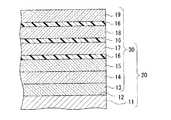
図3は、本発明に係る耐衝撃フィルムの他の実施形態を示す図である。
本発明の耐衝撃フィルムは、上述した第3の層15の視認側に、種々の機能を有する層を1層以上積層して構成することができる。これらの層としては、例えば、紫外線吸収層、色調補正層、近赤外線吸収(反射)層、防汚層、反射防止層、電磁波遮蔽層、ハードコート層、または耐擦傷性機能を与える層等を挙げることができる。
その一例として、図3に示す耐衝撃フィルム30は、第3の層15の視認側に、接着剤層16を介して電磁波遮蔽層17、近赤外線吸収機能と色調補正機能とを兼備した近赤外線吸収層18および反射防止層19を順に積層した構成になっている。なお、本例示は、平面型ディスプレイパネル本体11がPDPである場合に好ましい組み合わせを示すものであり、PDP以外の平面型ディスプレイパネル本体に適用する場合、または第1の層13と第2の層14と第3の層15のいずれかに電磁波遮蔽機能、近赤外線吸収機能および/または色調補正機能を付与してある場合などでは、電磁波遮蔽層17と近赤外線吸収層18の一方または両方を省いた構成としてよい。
以下に、本例示で挙げた各層の詳細を記す。
【0028】
[電磁波遮蔽層]
電磁波遮蔽層17は、PDP本体から放射される電磁波を遮蔽し、他の家電機器等に電磁波ノイズによる影響を及ぼさないようにするためのもので、PDP用の電磁波遮蔽層17としては、導電性金属のメッシュからなる導電層や、スパッタ法などの薄膜形成技術を用いて5〜20nmの金属膜、または該金属膜と酸化物とを多層に積層した導電性多層膜からなる透光性の導電層を用いることができる。導電性金属のメッシュからなる導電層は、PDP用の電磁波遮蔽(シールド)用メッシュとして従来より周知の各種メッシュ材を用いることができる。これらのメッシュ材に関しては、例えば特開平11−212475号公報、特開2000−156182号公報、特開2000−286593号公報等にも記載されている。
【0029】
透光性の導電層に用いる金属層としては、Au、AgおよびCuからなる群から選ばれる1種以上の金属又は該金属を主成分とする層が好ましく、特に、比抵抗が小さく、吸収が小さいことから、Agを主成分とする金属層が好ましい。さらにAgを主成分とする金属層としては、Agの拡散を抑制し、結果として耐湿性が向上することから、Agを主成分としPd、AuまたはCuの少なくとも一つを含む金属層であることが好ましい。Pd、AuまたはCuの少なくとも一つの含有割合は、AgとPd、AuまたはCuの少なくとも一つの含量との総量に対して0.3〜10原子%であることが好ましい。0.3原子%以上であればAgの安定化の効果が得られると共に、10原子%以下とすることで良好な耐湿性を維持しつつ、良好な成膜速度及び可視光透過率が得られる。したがって、以上の観点からは、添加量は5.0原子%以下が適当である。また、添加量が増加するとターゲットコストが著しく増加するので、通常必要な耐湿性を勘案すると、0.5〜2.0原子%程度の範囲となる。単層として透光性の導電層を形成する場合、この金属層の厚さは5〜20nm、好ましくは8〜15nmとされる。この金属層の形成方法は特に限定されないが、透明基板の一方の面側に直接、薄い金属膜を均一に成膜可能なスパッタ法を用いて成膜することが好ましい。
【0030】
この導電層としては、低いシート抵抗値、低い反射率、高い可視光線透過率が得られることから、透明な合成樹脂フィルムなどの適当な透明基板上に、酸化物層と金属層を交互に積層した多層導電膜、特に、酸化物層、金属層、酸化物層、と交互に計(2n+1)層(nは1以上の整数)積層された多層導電膜が好適に使用される。酸化物層としては、Bi、Zr、Al、Ti、Sn、InおよびZnからなる群から選ばれる1種以上の金属の酸化物を主成分とする層が挙げられる。好ましくはTi、Sn、InおよびZnからなる群から選ばれる1種以上の金属の酸化物を主成分とする層である。特に、吸収が小さく、屈折率が2前後であることから、ZnOを主成分とする層、屈折率が大きく、好ましい色調を少ない層数で得られやすいことからTiO2を主成分とする層が好ましい。酸化物層は、複数の薄い酸化物層から構成されていてもよい。例えば、ZnOを主成分とする酸化物層に代えて、SnO2を主成分とする層とZnOを主成分とする層とから形成することもできる。ZnOを主成分とする酸化物層は、Zn以外の1種以上の金属を含有するZnOからなる酸化物層であることが好ましい。含有された前記の1種以上の金属は、酸化物層中では主として酸化物の状態で存在している。1種以上の金属を含有するZnOとしては、Sn、Al、Cr、Ti、Si、B、MgおよびGaからなる群から選ばれる1種以上の金属を含有するZnOが好ましく挙げられる。前記1種以上の金属の含有割合は、得られる導電膜の耐湿性が向上することから、該金属の合計量とZnとの総量に対して1〜10原子%が好ましい。1原子%以上とすれば、充分にZnO膜の内部応力を低減せしめて、良好な耐湿性を得ることができる。また10原子%以下とすれば、ZnOの結晶性が良好に維持されると共に、金属層との相性が低下することがない。安定して再現性よく低内部応力のZnO膜を得ること、およびZnOの結晶性を考慮すると、金属の含有割合は2〜6原子%が好ましい。
酸化物層の幾何学的膜厚(以下、単に膜厚という)は、最も基板に近い酸化物層および最も透明基板から遠い酸化物層は20〜60nm(特に30〜50nm)、それ以外の酸化物層は40〜120nm(特に40〜100nm)とすることが好ましい。金属層の合計膜厚は、例えば得られる導電層の抵抗値の目標を2.5Ω/□とした場合、25〜40nm(特に25〜35nm)、抵抗値の目標を1.5Ω/□とした場合、35〜50nm(特に35〜45nm)とすることが好ましい。酸化物層と金属層との全合計膜厚は、例えば、金属層数が2の場合は150〜220nm(特に160〜200nm)、金属層数が3の場合は230〜330nm(特に250〜300nm)、金属層数が4の場合は270〜370nm(特に310〜350nm)であることが好ましい。
上記第1の金属層と第2の酸化物層との間、第2の金属層と第3の酸化物層との間、第3の金属層と第4の酸化物層との間には、酸化物層形成時に、金属層が酸化されることを防止するための別の層(以下、酸化バリア層という。)を設けることができる。酸化バリア層としては、例えば、金属層、酸化物層、窒化物層が用いられる。具体的には、Al、Ti、Si、GaおよびZnからなる群から選ばれる1種以上の金属、該金属の酸化物、窒化物などである。好ましくは、TiやSiとGaとを含有するZnOを用いる。酸化バリア層の膜厚は1〜7nmが望ましい。1nmより薄いとバリア層としての働きを充分に示さない。7nmより厚いと膜系の透過率が低下する。
【0031】
この電磁波遮蔽層17には、PDP本体から発した電磁波に起因して該層中で発生する電流をアース線に導くためのアース線接続用の電極(図示せず)が接続されている。この電極の形状および寸法は特に限定されないが、抵抗が低い方が電磁波遮蔽性能の点では優位となる。この電極は、耐衝撃フィルム30の周縁全体に設けることが、透光性導電膜の電磁波遮蔽効果を確保するために好ましい。このような電極は、例えば、Agペースト(Agとガラスフリットを含むペースト)やCuペースト(Cuとガラスフリットを含むペースト)を塗布、焼成して得られる電極が好適に用いられる。さらに、この電極に接続された図示しない長尺のアース線を含む構成とすることができる。
【0032】
[近赤外線吸収層]
近赤外線吸収層18は、PDP本体から放射される近赤外線を吸収する近赤外線吸収能を有する色素と、色調補正能を有する色素とを含有する透明な合成樹脂層から構成される。これらの色素は染料と顔料のいずれも使用できる。なお、「近赤外線吸収能を有する色素(以下、近赤外線吸収剤と記す。)」とは、少なくとも近赤外領域(波長780〜1300nm)の光の一部を吸収できる色素であればよく、該色素が他の波長領域、例えば可視光にも吸収能を有している色素であっても使用し得る。また「色調補正能を有する色素(以下、色調補正剤と記す。)」とは、可視光の波長領域(波長380〜780nm)の光を、好ましくは特定波長領域(複数の領域でもよい)の光を特異的に吸収できる色素である。近赤外線吸収剤および色調補正剤を含有させるベースの合成樹脂は特に限定されず、各種の透明な熱可塑性合成樹脂または熱硬化性合成樹脂を用いることができ、また該層の厚みは特に限定されないが、0.5〜25μm程度とするのが好ましい。
【0033】
近赤外線吸収剤としては、ポリメチン系、フタロシアニン系、ナフタロシアニン系、金属錯体系、アミニウム系、イモニウム系、ジイモニウム系、アンスラキノン系、ジチオール金属錯体系、ナフトキノン系、インドールフェノール系、アゾ系、トリアリルメタン系の化合物などが挙げられるが、これらに限定されない。熱線吸収や電子機器のノイズ防止の用途には、最大吸収波長が750〜1100nmである近赤外線吸収剤が好ましく、金属錯体系、アミニウム系、フタロシアニン系、ナフタロシアニン系、ジイモニウム系が特に好ましい。近赤外線吸収剤は1種類としてもよいし、2種以上を混合して用いてもよい。
【0034】
色調補正剤は、可視光の特定波長域の一部を吸収し、透過可視光の色調を改善するために用いられる。本発明において使用し得る色調補正剤としては、アゾ系、縮合アゾ系、ジインモニウム系、フタロシアニン系、アンスラキノン系、インジゴ系、ペリノン系、ペリレン系、ジオキサジン系、キナクリドン系、メチン系、イソインドリノン系、キノフタロン系、ピロール系、チオインジゴ系、金属錯体系などの周知の有機顔料および有機染料、無機顔料が挙げられるが、耐候性が良好であるとともに近赤外線吸収層18の主剤との相溶性または分散性が良好な色素、例えばジインモニウム系、フタロシアニン系、アンスラキノン系色素のうちの1種類又は2種以上を適宜組み合わせて用い得る。
【0035】
この耐衝撃フィルム30をPDPに適用する場合、近赤外線吸収剤により、PDPの表示画面から発せられる近赤外線が近赤外線吸収層18に吸収され、電子機器に対するノイズ発生を防止することができる。また近赤外線吸収層18に含有させる色調補正剤としては、PDP本体内に封入された放電ガス、例えばネオンとキセノンの二成分ガス、からの余分な発光色(主に560〜610nmに波長領域)を選択的に吸収・減衰させるための1種類若しくは複数種類の色調補正剤を混合して含有させることが好ましい。このような色素構成とすることによって、PDPの表示画面から発せられる可視光のうち、放電ガスの発光に起因する余分な光が吸収・減衰され、その結果PDPの表示画面から発する可視光の表示色を表示目標の表示色に近づけることができ、自然な色調を表示し得るPDPを提供できる。このように上記放電ガスからの余分な発光色を選択的に吸収・減衰させる色素には、近赤外線を吸収・減衰させる効果を有するものもある。
【0036】
[反射防止層]
反射防止層19は、反射防止性を有している層であればよく、既知の反射防止方法が何でも採用できる。例えば防眩性(アンチグレア)処理を施した層または低屈折率層を含む層であればよい。高剛性透明基板自身が万一破損した際に破片の飛散防止の観点から、樹脂フィルムの片面に、低屈折率層を有しているものが好ましい。特にポリウレタン系軟質樹脂の片面に非結晶性の含フッ素重合体からなる低屈折率層を有する反射防止層が好ましく、具体的には旭硝子社製のアークトップ(商品名)などが挙げられる。また最外面層となる反射防止層19の表面に、耐摩耗性を付与させるため潤滑剤を反射防止性能を損なわない程度に塗布したり、反射防止層19中に潤滑剤を配合したりしてもよい。このような潤滑剤として、デュポン社製の商品名クライトックス、ダイキン工業社製の商品名ダイフロイル、アウジモント社製の商品名フォンブリン、旭硝子社製の商品名フロンルーブなどのパーフルオロポリエーテル類が挙げられる。
【0037】
反射防止層19に上述したアークトップ(商品名)のような飛散防止兼反射防止樹脂フィルムを用いる場合、そのポリウレタン樹脂層中に近赤外線吸収剤を混入しておき、この反射防止層19に近赤外線遮蔽効果を持たせてもよい。また、特定波長の可視光を吸収する顔料および/または染料を含有せしめることで、表示色の色バランスを補正する色調補正能を持たせることもできる。
【0038】
[接着剤層]
上記第3の層15と電磁波遮蔽層17の間、電磁波遮蔽層17と近赤外線吸収層18との間、および近赤外線吸収層18と反射防止層19との間は、透明な接着剤層16を介して接着し得る。好適な接着剤としては、エチレン−酢酸ビニル共重合体(EVA)等のホットメルト型の接着剤、エポキシ、アクリレート系の紫外線硬化型、熱硬化型接着剤を挙げることができる。接着剤層16の厚さは各々0.1〜1.0mm、好ましくは0.2〜0.5mmとする。
【0039】
本実施形態の耐衝撃フィルム30は、平面型ディスプレイパネル本体11の前面ガラス12に接合した状態で、衝撃を受けた際、第3の層15で衝撃力が分散、吸収され、さらに第2の層14と前面ガラス12の間に設けられた軟質な第1の層13によって衝撃が吸収されて前面ガラス12への衝撃力の伝達が防止され、軽量、薄型で耐衝撃性の優れた耐衝撃フィルムを提供できる、という先の実施態様の耐衝撃フィルム10と同様の効果を得ることができる他、第3の層15の視認側面に、電磁波遮蔽層17と、近赤外線吸収能と色調補正能とを兼備する近赤外線吸収層18と、反射防止層19とを積層形成したことによって、平面型ディスプレイパネル本体11として、PDPのように、電磁波や近赤外線によるノイズが発生しかつ表示色の色バランスを補正することが望ましいディスプレイパネルに特に好適に適用させることができる。
【0040】
【実施例】
以下、本発明の耐衝撃フィルムの効果を具体的に記す。以下の例1〜5は本発明に係る実施例であり、例6〜8は比較例を示す。
【0041】
(例1)
ガラス基板の作製:厚さ2.8mmの高歪み点ガラス(商品名:PD200、旭硝子社製)に、透明電極、バス電極、透明誘電体および保護膜を順次積層し、縦950mm×横540mmのPDPの前面ガラスを模したガラス基板を作製した。これら各層は次のような条件で作製した。
透明電極:ITOをスパッタリング法により成膜し、フォトリソグラフィーにより電極パターンを作製した。
バス電極:Cr−Cu−Crの三層をスパッタリング法により成膜し、フォトリソグラフィーにより電極パターンを作製した。
透明誘電体:ペースト状にした低融点ガラスをベタ印刷により成膜した。
保護膜:透明誘電体の表面に接着(シール)層をスクリーン印刷により成膜した後、MgOを蒸着法により成膜した。
【0042】
第1の層として、せん断弾性率が4.6×10³Paのシリコーン樹脂(商品名:αGEL、ジェルテック社製)からなる厚さ2.0mmのフィルムと、第2の層として、ポリカーボネート(商品名:レキサン8010、旭硝子社製)からなる厚さ1.0mmのフィルムとを、ゴムロールを用いて室温でラミネートし、さらにポリカーボネート側に、第3の層として、厚さ0.2mmからなるポリウレタンフィルムに反射防止層および粘着剤層を積層したフィルム(商品名:アークトップUR2199NF、旭硝子社製)を、ゴムロールによりラミネートして耐衝撃フィルムを作製した。なお、前記ポリカーボネートおよびポリウレタンの引張弾性率から換算したせん断弾性率はそれぞれ9.0×10⁹Paおよび6.7×10⁶Paであった。
この耐衝撃フィルムと上記ガラス基板を、耐衝撃フィルムのシリコーン樹脂面がガラス基板に接触するように、ゴムロールを用いて室温でラミネートし、耐衝撃フィルム付きのガラス基板(以下、耐衝撃ガラス基板と記す。)を作製した。
この耐衝撃ガラス基板(例1)を用い、以下の条件で衝撃試験および耐熱性試験を実施した。結果を表1に記す。
【0043】
[評価方法]
せん断弾性率G´:Rheometric Scientific社製の動的粘弾性測定装置ARESを用い、周波数1Hz、温度25℃の条件で直接測定した。ただし、ポリカーボネート等のせん断弾性率は、上記装置を用いて、温度25℃にて引張弾性率(E)を測定し、換算式E=3G´に従って、引張弾性率をせん断弾性率に換算して得た。特に記載しない限り、前記の方法でせん断弾性率を直接測定した。
【0044】
衝撃試験:IEC規格(Publication 65.1985)に記載されたスプリングインパクトハンマー(MODEL F−22、ドイツPTL社製)を用いて、0.2J、0.35J、0.50J、0.70Jおよび1.00Jの衝撃力で評価を行なった。割れなかった場合を○、割れた場合を×とした。なお、電気用品取締法に規定されているポリアミド加工したおもり(半径10mm、250g)を約20.4cmの高さから落下させたときの衝撃エネルギーは、0.50Jと一致することから、本衝撃試験において0.50J以上の耐衝撃性を有すれば、実用上十分な耐衝撃性を有しているものと判断できる。
衝撃試験は、該耐衝撃ガラス基板を、アルミニウム製の板(厚み10mm×縦1000mm×横600mm)上に置き、万力で四辺を固定してコンクリート壁に立て掛けて実施した。
【0045】
耐熱性試験:80℃のオーブン中に入れ、1000時間経過した後に取り出し、外観を観察した。オーブンに入れる前と比較して変化がない場合を○、耐衝撃フィルムがガラス基板から剥がれた場合、またはフィルムとガラス基板の間に気泡の発生や表面状態の歪みを生じた場合を×とした。
【0046】
(例2)
シリコーン樹脂溶液(商品名:SD4560、東レ・ダウコーニング・シリコーン社製)の100質量部およびシリコーン樹脂用硬化剤(商品名:SRX212、東レ・ダウコーニング・シリコーン社製)の0.9質量部とを混合して、シリコーン粘着剤を調製した。
このシリコーン粘着剤を、バーコーターを用いて、例1で用いたシリコーン樹脂からなるフィルムの両面に塗工し、100℃にて10分間乾燥およびアニール処理することにより、両面に0.015mmのシリコーン粘着剤が積層されたシリコーン樹脂フィルムを得た。
例1のシリコーン樹脂からなるフィルム(第1の層)を、該シリコーン樹脂フィルムに変更した以外は、例1と同様に操作して、耐衝撃ガラス基板を作製し、例1と同様の試験を実施した。結果を表1に記す。
【0047】
(例3)
例2のシリコーン樹脂からなるフィルムを、せん断弾性率が4.1×10⁵Paのシリコーン樹脂(商品名:θ―8、ジェルテック社製)からなる厚さ2.0mmのフィルムに変更した以外は、例1と同様に操作して、耐衝撃ガラス基板を作製し、例1と同様の試験を実施した。結果を表1に記す。
【0048】
(例4)
プレミノールPML−3012(商品名、旭硝子社製のポリエーテル系ポリオール)の65質量部、エクセノールEL−1030(商品名、旭硝子社製のポリエーテル系ポリオール)の28質量部、プレミノールPML−1003(商品名、旭硝子社製のポリエーテル系ポリオール)の100質量部、ヘキサメチレンジイソシアネートの30質量部、ジブチル錫ジラウレートの0.2質量部および酸化防止剤(商品名:IRGANOX 1010、チバガイギー社製)の2質量部とを混合し、脱泡後、離型処理を施したポリエチレンテレフタレートフィルム上に流延し、80℃で20分間反応させて、厚さ2.0mmのポリウレタンフィルムを得た。このポリウレタンフィルムのせん断弾性率は3.1×10⁵Paであった。
このポリウレタンフィルムの両面に、アクリル系粘着剤(綜研化学社製、商品名:SKダイン1604Nの150質量部と綜研化学社製、商品名:L−45の2質量部とを混合したもの)を、バーコーターを用いて塗工し、100℃にて10分間、乾燥およびアニール処理することにより、両面に0.015mmのアクリル系粘着剤が積層されたポリウレタンフィルムを得た。
例1のシリコーン樹脂からなるフィルムを、該ポリウレタンフィルムに変更した以外は、例1と同様に操作して、耐衝撃ガラス基板を作製し、例1と同様の試験を実施した。結果を表1に記す。
【0049】
(例5)
例1で使用したシリコーン樹脂フィルム(第1の層)と、ポリエチレンテレフタレート(商品名:A4300、東洋紡績社製)からなる厚さ0.1mmのフィルム(第2の層)と、第3の層として例1で使用したポリウレタンフィルムおよび反射防止層をそれぞれ積層したフィルム(商品名:アークトップUR2150、旭硝子社製)とを順に重ね合わせ、ゴムロールを用いて室温でラミネートして耐衝撃フィルムを作製し、さらに例1と同様に操作して耐衝撃ガラス基板を作製し、例1と同様の試験を実施した。
【0050】
(例6)
耐衝撃フィルムを接合しないガラス基板のみで衝撃試験を実施した。結果を表1に記す。
【0051】
(例7)
ポリカーボネート(商品名:レキサン8010、旭硝子社製、せん断弾性率9.0×10⁹Pa)からなる厚さ2.0mmのフィルムの片面にアクリル系粘着剤(綜研化学社製、商品名:SKダイン1604Nの150質量部と綜研化学社製、商品名:L−45の2質量部とを混合したもの)を厚さ0.015mmになるように積層して、粘着剤面がガラス基板に接触するように、ゴムロールを用いて室温でラミネートし、衝撃吸収フィルム付きのガラス基板を作製し、例1と同様の試験を実施した。結果を表1に記す。
【0052】
(例8)
厚さ0.8mmのポリプロピレン/EVA/ポリプロピレンフィルム(商品名:POVIC−T、アキレス社製)の両面にアクリル系粘着剤(綜研化学社製、商品名:SKダイン1604Nの150質量部と綜研化学社製、商品名:L−45の2質量部とを混合したもの)を積層し、その片面にポリエチレンテレフタレート(商品名:コスモシャインA4300、東洋紡社製)からなる厚さ0.188mmのフィルムをゴムロールを用いて室温でラミネートした。
ポリプロピレン/EVA/ポリプロピレンフィルムおよびポリエチレンテレフタレートフィルムのせん断弾性率は、引張弾性率から換算し、それぞれ6.9×107Pa、2.0×109Paであった。この衝撃吸収フィルムと上記ガラス基板とを、衝撃吸収フィルムの粘着剤面がガラス基板に接触するように、ゴムロールを用いて室温でラミネートし、衝撃吸収フィルム付きのガラス基板を作製し、例1と同様の試験を実施した。結果を表1に記す。
【0053】
【表1】
表1の結果から判るように、本発明に係る例1〜5の耐衝撃フィルムは、PDPの前面ガラスに模して作製したガラス基板に接合し、耐衝撃ガラス基板とした状態で、全てが実用上十分な耐衝撃性を有しているものと判断できる0.50J以上の耐衝撃性を有していた。
一方、耐衝撃フィルムを接合しない例6のガラス基板は、0.2Jより低い耐衝撃性であった。
また、このガラス基板に、厚さ2.0mmのポリカーボネート層を、薄い粘着剤層を介して接合した例7の耐衝撃ガラス基板は、0.2Jより低い耐衝撃性であった。このことから、ガラス基板に硬質の樹脂フィルムを接合しただけでは耐衝撃性が増加しないことが判る。
さらに、従来積層体に模して作製した積層体を接合した例8の耐衝撃ガラス基板は、0.2Jより低い耐衝撃性であり、本発明に係る例1〜5の各耐衝撃ガラス基板に比べ、明らかに耐衝撃性が劣っていた。さらに、例8の耐衝撃ガラス基板は、第1の層として熱可塑性樹脂を用いていることから、耐熱性が不十分であり、PDP用の耐衝撃フィルムとして好ましくなかった。
【0055】
【発明の効果】
本発明により、平面型パネルディスプレイパネルの前面ガラスに接合することで、衝撃によるガラス破砕を防止できるとともに、軽量化および薄型化を可能にした平面型ディスプレイパネル用耐衝撃フィルムおよび平面型ディスプレイパネルを提供できる。
【図面の簡単な説明】
【図1】 PDPの構成を説明するための要部斜視図である。
【図2】 本発明に係る耐衝撃フィルムおよび平面型ディスプレイパネルの一実施形態を示す断面図である。
【図3】 本発明に係る耐衝撃フィルムおよび平面型ディスプレイパネルの他の実施形態を示す断面図である。
【符号の説明】
10,30 耐衝撃フィルム(平面型ディスプレイパネル用耐衝撃フィルム)
11 平面型ディスプレイパネル本体
12 前面ガラス
13 第1の層
14 第2の層
15 第3の層
16 接着剤層
17 電磁波遮蔽層
18 近赤外線吸収層
19 反射防止層
20 平面型ディスプレイパネル[0001]
BACKGROUND OF THE INVENTION
The present invention is attached to a front glass of a flat display panel, prevents the front glass from being shattered by an impact, and reduces the weight and thickness of the impact resistant film for a flat display panel and a flat type using the same. It relates to a display panel.
[0002]
[Prior art]
In recent years, a plasma display panel (hereinafter abbreviated as PDP) having an advantage that a large screen panel can be manufactured and a clear full color display is possible has attracted attention. The PDP performs full color display by selectively causing a phosphor to discharge light in a large number of discharge cells formed between two glass plates.
[0003]
FIG. 1 is a diagram illustrating the structure of a PDP. A PDP denoted by reference numeral 1 in this figure has a configuration in which a
The
[0004]
Conventionally, in order to prevent damage to the front glass of a flat display panel such as a PDP, a protective plate made of acrylic resin or tempered glass is provided at a distance of several millimeters in front of the front glass. The impact was prevented. However, such a protective structure has a problem that obstructs the weight reduction and thickness reduction of the flat display panel. Furthermore, since there is a space between the front glass of the panel and the protective plate, there is a problem that image quality is deteriorated due to reflection of external light such as a fluorescent lamp, and image distortion is caused by slight vibration.
[0005]
Various techniques for preventing damage to the front glass of the flat display panel have been proposed so far. For example, Japanese Patent Application Laid-Open No. 2000-123751 discloses a technique for improving the strength by increasing the thickness of the front glass. Has been proposed. However, this structure has a problem in that the protection effect against impact is insufficient and the panel weight increases.
In JP 2000-156182 A, JP 11-119667 A, JP 11-119668 A, and JP 11-119669 A, a protective plate is bonded to the front glass of the panel through an adhesive layer. However, in this structure, there is a problem that an impact is easily transmitted to the front glass, and the front glass cannot be sufficiently damaged.
[0006]
As another prior art, Japanese Patent Laid-Open No. 2001-266759 discloses a crack prevention layer (impact mitigation layer) B and a scattering prevention layer thereon through a transparent adhesive layer on the front glass of a flat display panel. Two layers of transparent synthetic resin are laminated in order with A, and the shear elastic modulus of the scattering prevention layer A is 2 × 10.8 Pa or higher, and the shear modulus of the crack prevention layer B is 1 × 10Four ~ 2x10⁸ An impact relaxation laminate (hereinafter referred to as a conventional laminate) in the range of Pa has been proposed.
[0007]
[Problems to be solved by the invention]
However, the above conventional laminate is insufficient in terms of imparting impact resistance to a front glass such as PDP. In the examples of the publication, as a glass plate, an electrode or a thin film made of various materials is not laminated, so to speak, an “untreated” glass plate is used, and an adhesive, an impact relaxation layer, and scattering prevention are used for this. The layers are stacked in order and the hard balls are dropped and tested for impact resistance. However, as described above, the front glass of an actual PDP is the result of stacking electrodes and thin films made of various materials. Compared to the treated glass, the impact resistance is greatly deteriorated and it is easy to break. As described above, it has not been demonstrated that the conventional laminate can obtain a sufficient impact resistance effect when bonded to the front glass of PDP whose impact resistance is significantly weaker than that of an untreated glass plate. And, as will be described in detail in the examples described later, a glass substrate on which an electrode or a dielectric film is formed on a glass plate and a front glass of a PDP is assumed, and a material equivalent to that described in the examples of the publication When three layers of thickness were laminated and the impact resistance was measured by applying a predetermined impact force with a spring impact hammer, it was found that this was insufficient in impact resistance (see Example 8 of the Example). .
Therefore, the conventional laminate is insufficient as an impact resistant film for protecting the front glass of a flat display panel such as a PDP whose impact resistance is weakened.
[0008]
The present invention is attached to the front surface of a flat display panel, prevents the glass from being shattered and scattered when subjected to an impact, and is capable of reducing the weight and thickness of the impact resistant film (hereinafter referred to as a flat display panel). It is abbreviated as impact-resistant film.) And a flat display panel using the same.
[0009]
[Means for Solving the Problems]
In order to achieve the above object, the present invention provides an impact resistant film bonded to a front glass of a flat display panel body, and has a shear modulus of 1 × 10.Three Pa ~ 1x10⁶ It is made of a transparent synthetic resin of Pa, the first layer on the front glass side of the flat display panel, and the shear modulus is 1 × 10⁸ It is made of a transparent synthetic resin of Pa or higher, and has a second layer closer to the viewing side than the first layer, and a shear modulus of 1 × 10⁶ Pa or more 1 × 10⁸ An impact-resistant film for a flat display panel, comprising a transparent synthetic resin of less than Pa and including a third layer closer to the viewing side than the second layer.
The impact resistant film of the present invention has a shear modulus of 1 × 10.8 Between the second layer made of hard synthetic resin of Pa or higher and the front glass of the flat display panel, the shear elastic modulus is 1 × 10Three Pa ~ 1 × 10⁶ While providing the 1st layer which consists of a soft synthetic resin of Pa, the shear elastic modulus is 1 * 10 in the visual recognition side of the 2nd layer.6 Pa or more 1 × 10⁸ Since the third layer of less than Pa is laminated, when receiving an impact, the impact force is dispersed and absorbed by the third layer, and a soft layer provided between the second layer and the front glass. The impact is absorbed by the first layer and the transmission of impact force to the front glass is prevented, and a lightweight, thin, and impact resistant film with excellent impact resistance can be provided.
[0010]
The impact-resistant film of the present invention preferably has a structure in which the second layer is laminated on the viewing side surface of the first layer.
The first layer is preferably an adhesive resin material that is directly bonded to the front glass of the flat display panel.
Furthermore, the thickness of the first layer is in the range of 1.0 to 4.0 mm, the thickness of the second layer is 0.05 to 3.0 mm, and the thickness of the third layer is 0.00. It is desirable that it is 05-2.0 mm.
Further, at least one layer selected from the group consisting of an electromagnetic wave shielding layer, a near-infrared absorbing layer, and an antireflection layer, and an adhesive layer that bonds these layers are laminated on the viewing side of the second layer. The configuration may be good.
[0011]
Furthermore, the present invention provides a flat display panel in which the above-mentioned impact resistant film is bonded to the front glass of the flat display panel main body directly or via a transparent adhesive layer.
[0012]
DETAILED DESCRIPTION OF THE INVENTION
FIG. 2 is a view showing an example of the impact resistant film of the present invention. The impact
[0013]
The shear modulus (G ′) is a measured value of the shear modulus G ′ at 25 ° C. ± 3 ° C. at a frequency of 1 Hz using a dynamic viscoelasticity measuring device DMS120 manufactured by Seiko Instruments Inc. In general, there is a relationship of tensile elastic modulus E = 3G ′ (shear elastic modulus), and the tensile elastic modulus E is about three times the shear elastic modulus.
[0014]
[First layer]
The
[0015]
The shear modulus of the
Furthermore, among thermosetting resins having a shear elastic modulus in the above range, those having adhesiveness, for example, silicone films manufactured by Geltech Co., Ltd., trade names αGEL, θ-5, θ-6, θ-7 and θ− The resin material such as 8 can be easily laminated on the viewing side surface of the
[0016]
The thickness of the
[0017]
In the
[0018]
When a thermosetting resin such as a urethane resin and a silicone resin is used as the material of the
[0019]
[Second layer]
The
[0020]
The thickness of the
[0021]
[Third layer]
The
[0022]
The thickness of the
[0023]
As a preferred example of this embodiment, the
[0024]
The impact
[0025]
[Flat display panel]
As shown in FIG. 2, the
[0026]
As the flat display panel
[0027]
FIG. 3 is a view showing another embodiment of the impact resistant film according to the present invention.
The impact resistant film of the present invention can be constituted by laminating one or more layers having various functions on the viewing side of the
As an example, the impact-
Below, the detail of each layer quoted by this illustration is described.
[0028]
[Electromagnetic wave shielding layer]
The electromagnetic
[0029]
The metal layer used for the translucent conductive layer is preferably one or more metals selected from the group consisting of Au, Ag and Cu, or a layer containing the metal as a main component, particularly having a small specific resistance and absorption. Since it is small, the metal layer which has Ag as a main component is preferable. Further, the metal layer containing Ag as a main component is a metal layer containing Ag as a main component and containing at least one of Pd, Au, or Cu because the diffusion of Ag is suppressed and, as a result, moisture resistance is improved. Is preferred. The content ratio of at least one of Pd, Au, or Cu is preferably 0.3 to 10 atomic% with respect to the total amount of Ag and at least one content of Pd, Au, or Cu. If it is 0.3 atomic% or more, the effect of stabilizing Ag can be obtained, and if it is 10 atomic% or less, good film formation speed and visible light transmittance can be obtained while maintaining good moisture resistance. . Therefore, from the above viewpoint, the addition amount is suitably 5.0 atomic% or less. Moreover, since target cost will increase remarkably when an addition amount increases, when it considers normally required moisture resistance, it will be the range of about 0.5-2.0 atomic%. When a translucent conductive layer is formed as a single layer, the thickness of the metal layer is 5 to 20 nm, preferably 8 to 15 nm. The method for forming this metal layer is not particularly limited, but it is preferable to form the metal layer directly on one surface side of the transparent substrate using a sputtering method capable of uniformly forming a thin metal film.
[0030]
As this conductive layer, low sheet resistance, low reflectance, and high visible light transmittance can be obtained, so an oxide layer and a metal layer are alternately laminated on a transparent substrate such as a transparent synthetic resin film. In particular, a multilayer conductive film in which a total of (2n + 1) layers (n is an integer of 1 or more) are alternately laminated with an oxide layer, a metal layer, and an oxide layer is preferably used. Examples of the oxide layer include a layer mainly composed of an oxide of one or more metals selected from the group consisting of Bi, Zr, Al, Ti, Sn, In, and Zn. Preferably, it is a layer mainly composed of an oxide of one or more metals selected from the group consisting of Ti, Sn, In and Zn. In particular, since the absorption is small and the refractive index is around 2, a layer mainly composed of ZnO, a refractive index is large, and a preferable color tone can be easily obtained with a small number of layers.2 A layer containing as a main component is preferred. The oxide layer may be composed of a plurality of thin oxide layers. For example, instead of an oxide layer mainly composed of ZnO, SnO2 It can also be formed from a layer containing ZnO as a main component and a layer containing ZnO as a main component. The oxide layer mainly composed of ZnO is preferably an oxide layer made of ZnO containing one or more metals other than Zn. The one or more metals contained are present mainly in an oxide state in the oxide layer. Preferred examples of ZnO containing one or more metals include ZnO containing one or more metals selected from the group consisting of Sn, Al, Cr, Ti, Si, B, Mg, and Ga. The content ratio of the one or more metals is preferably 1 to 10 atomic% with respect to the total amount of the metal and the total amount of Zn because the moisture resistance of the obtained conductive film is improved. If it is 1 atomic% or more, the internal stress of the ZnO film can be sufficiently reduced, and good moisture resistance can be obtained. Moreover, if it is 10 atomic% or less, the crystallinity of ZnO will be maintained satisfactorily and compatibility with the metal layer will not be reduced. In consideration of obtaining a ZnO film having a low internal stress stably with good reproducibility, and considering the crystallinity of ZnO, the metal content is preferably 2 to 6 atomic%.
The geometric thickness of the oxide layer (hereinafter simply referred to as the film thickness) is 20 to 60 nm (particularly 30 to 50 nm) for the oxide layer closest to the substrate and the oxide layer farthest from the transparent substrate, and other oxidations. The physical layer is preferably 40 to 120 nm (particularly 40 to 100 nm). The total thickness of the metal layers is, for example, 25 to 40 nm (especially 25 to 35 nm) when the resistance value target of the obtained conductive layer is 2.5 Ω / □, and the resistance value target is 1.5 Ω / □. In this case, the thickness is preferably 35 to 50 nm (particularly 35 to 45 nm). The total thickness of the oxide layer and the metal layer is, for example, 150 to 220 nm (especially 160 to 200 nm) when the number of metal layers is 2, and 230 to 330 nm (especially 250 to 300 nm) when the number of metal layers is 3. ), When the number of metal layers is 4, it is preferably 270 to 370 nm (particularly 310 to 350 nm).
Between the first metal layer and the second oxide layer, between the second metal layer and the third oxide layer, and between the third metal layer and the fourth oxide layer. In forming the oxide layer, another layer (hereinafter referred to as an oxidation barrier layer) for preventing the metal layer from being oxidized can be provided. For example, a metal layer, an oxide layer, or a nitride layer is used as the oxidation barrier layer. Specifically, one or more metals selected from the group consisting of Al, Ti, Si, Ga and Zn, oxides and nitrides of the metals, and the like. Preferably, ZnO containing Ti, Si and Ga is used. The film thickness of the oxidation barrier layer is desirably 1 to 7 nm. When it is thinner than 1 nm, it does not sufficiently function as a barrier layer. If it is thicker than 7 nm, the transmittance of the membrane system is lowered.
[0031]
The electromagnetic
[0032]
[Near-infrared absorbing layer]
The near-infrared
[0033]
Near-infrared absorbers include polymethine, phthalocyanine, naphthalocyanine, metal complex, aminium, imonium, diimonium, anthraquinone, dithiol metal complex, naphthoquinone, indolephenol, azo, tri Examples include, but are not limited to, allylmethane-based compounds. For applications such as heat ray absorption and noise prevention of electronic devices, near infrared absorbers having a maximum absorption wavelength of 750 to 1100 nm are preferable, and metal complex-based, aminium-based, phthalocyanine-based, naphthalocyanine-based, and diimonium-based are particularly preferable. A near-infrared absorber is good also as 1 type, and may mix and
[0034]
The color tone correction agent is used to absorb a part of a specific wavelength range of visible light and improve the color tone of transmitted visible light. Examples of the color correction agent that can be used in the present invention include azo, condensed azo, diimmonium, phthalocyanine, anthraquinone, indigo, perinone, perylene, dioxazine, quinacridone, methine, and isoindolinone. Well-known organic pigments and organic dyes such as quinophthalone, pyrrole, thioindigo, and metal complex, and inorganic pigments. The weather resistance is good and the compatibility with the main component of the near-
[0035]
When this impact
[0036]
[Antireflection layer]
The
[0037]
When the anti-scattering and anti-reflection resin film such as the above-mentioned arc top (trade name) is used for the
[0038]
[Adhesive layer]
A
[0039]
The impact
[0040]
【Example】
Hereinafter, the effect of the impact resistant film of the present invention will be specifically described. Examples 1 to 5 below are examples according to the present invention, and Examples 6 to 8 show comparative examples.
[0041]
(Example 1)
Fabrication of glass substrate: A transparent electrode, a bus electrode, a transparent dielectric, and a protective film were sequentially laminated on a high strain point glass (trade name: PD200, manufactured by Asahi Glass Co., Ltd.) having a thickness of 2.8 mm, and a length of 950 mm x 540 mm A glass substrate imitating the front glass of PDP was produced. Each of these layers was produced under the following conditions.
Transparent electrode: ITO was formed into a film by a sputtering method, and an electrode pattern was prepared by photolithography.
Bus electrode: Three layers of Cr—Cu—Cr were formed by sputtering, and an electrode pattern was prepared by photolithography.
Transparent dielectric: Paste-like low melting point glass was formed by solid printing.
Protective film: An adhesive (seal) layer was formed on the surface of the transparent dielectric by screen printing, and then MgO was formed by vapor deposition.
[0042]
As the first layer, the shear modulus is 4.6 × 10Three A film having a thickness of 2.0 mm made of a silicone resin of Pa (trade name: αGEL, manufactured by Geltech Co.) and a thickness of 1. 2 mm made of polycarbonate (trade name: Lexan 8010, manufactured by Asahi Glass Co., Ltd.). A film obtained by laminating a 0 mm film at room temperature using a rubber roll and further laminating an antireflection layer and an adhesive layer on a polyurethane film having a thickness of 0.2 mm as a third layer on the polycarbonate side (trade name) : ARCTOP UR2199NF, manufactured by Asahi Glass Co., Ltd.) was laminated with a rubber roll to produce an impact resistant film. The shear modulus converted from the tensile modulus of the polycarbonate and polyurethane is 9.0 × 10.9 Pa and 6.7 × 10⁶ Pa.
The impact resistant film and the glass substrate are laminated at room temperature using a rubber roll so that the silicone resin surface of the impact resistant film is in contact with the glass substrate, and a glass substrate with an impact resistant film (hereinafter referred to as an impact resistant glass substrate and It was written.)
Using this impact resistant glass substrate (Example 1), an impact test and a heat resistance test were performed under the following conditions. The results are shown in Table 1.
[0043]
[Evaluation methods]
Shear elastic modulus G ′: Using a dynamic viscoelasticity measuring device ARES manufactured by Rheometric Scientific, directly measured under conditions of a frequency of 1 Hz and a temperature of 25 ° C. However, for the shear modulus of polycarbonate and the like, the tensile modulus (E) is measured at a temperature of 25 ° C. using the above-mentioned apparatus, and the tensile modulus is converted into the shear modulus according to the conversion formula E = 3G ′. Obtained. Unless otherwise stated, the shear modulus was directly measured by the method described above.
[0044]
Impact test: 0.2J, 0.35J, 0.50J, 0.70J and 1 using a spring impact hammer (MODEL F-22, manufactured by PTL, Germany) described in the IEC standard (Publication 65.1985) Evaluation was performed with an impact force of 0.000 J. The case where it did not break was marked with ◯, and the case where it broke was marked with ×. The impact energy when dropping a weight (radius 10mm, 250g) stipulated in the Electrical Appliance and Material Control Law from a height of about 20.4cm is equal to 0.50J. If it has an impact resistance of 0.50 J or more in the test, it can be determined that it has practically sufficient impact resistance.
The impact test was performed by placing the impact-resistant glass substrate on an aluminum plate (
[0045]
Heat resistance test: placed in an oven at 80 ° C., taken out after 1000 hours, and observed for appearance. The case where there is no change compared with before putting in the oven is ○, the case where the impact-resistant film is peeled off from the glass substrate, or the case where bubbles are generated between the film and the glass substrate or the surface condition is distorted is indicated as x. .
[0046]
(Example 2)
100 parts by mass of a silicone resin solution (trade name: SD4560, manufactured by Toray Dow Corning Silicone) and 0.9 parts by mass of a curing agent for silicone resin (trade name: SRX212, manufactured by Toray Dow Corning Silicone) Were mixed to prepare a silicone adhesive.
This silicone pressure-sensitive adhesive was applied to both sides of the film made of the silicone resin used in Example 1 using a bar coater, and dried and annealed at 100 ° C. for 10 minutes, whereby 0.015 mm silicone on both sides. A silicone resin film laminated with an adhesive was obtained.
An impact-resistant glass substrate was prepared in the same manner as in Example 1 except that the silicone resin film (first layer) in Example 1 was changed to the silicone resin film, and the same test as in Example 1 was performed. Carried out. The results are shown in Table 1.
[0047]
(Example 3)
The film made of the silicone resin of Example 2 has a shear modulus of 4.1 × 10Five An impact-resistant glass substrate was prepared in the same manner as in Example 1 except that the film was changed to a 2.0 mm thick film made of Pa silicone resin (trade name: θ-8, manufactured by Geltech). The same test as 1 was performed. The results are shown in Table 1.
[0048]
(Example 4)
65 parts by mass of preminol PML-3012 (trade name, polyether polyol manufactured by Asahi Glass Co., Ltd.), 28 parts by mass of Exenol EL-1030 (trade name, polyether polyol manufactured by Asahi Glass Co., Ltd.), preminol PML-1003 (product) Name, 100 parts by mass of polyether polyol manufactured by Asahi Glass Co., Ltd., 30 parts by mass of hexamethylene diisocyanate, 0.2 parts by mass of dibutyltin dilaurate, and antioxidant (trade name: IRGANOX 1010, manufactured by Ciba Geigy) After mixing with parts by mass and defoaming, the mixture was cast on a polyethylene terephthalate film that had been subjected to a release treatment and reacted at 80 ° C. for 20 minutes to obtain a polyurethane film having a thickness of 2.0 mm. The shear modulus of this polyurethane film is 3.1 × 10Five Pa.
Acrylic adhesive (trade name: SK Dyne 1604N 150 parts by mass and Soken Chemicals Co., Ltd., trade name: L-45 2 parts by mass) was mixed on both sides of this polyurethane film. Then, coating was performed using a bar coater, followed by drying and annealing at 100 ° C. for 10 minutes to obtain a polyurethane film having 0.015 mm acrylic adhesive laminated on both sides.
An impact resistant glass substrate was produced in the same manner as in Example 1 except that the film made of the silicone resin in Example 1 was changed to the polyurethane film, and the same test as in Example 1 was performed. The results are shown in Table 1.
[0049]
(Example 5)
Silicone resin film (first layer) used in Example 1, 0.1 mm thick film (second layer) made of polyethylene terephthalate (trade name: A4300, manufactured by Toyobo Co., Ltd.), and third layer As an example, the polyurethane film used in Example 1 and a film laminated with an antireflection layer (trade name: Arc Top UR2150, manufactured by Asahi Glass Co., Ltd.) are sequentially stacked and laminated at room temperature using a rubber roll to produce an impact resistant film. Further, an impact-resistant glass substrate was produced in the same manner as in Example 1, and the same test as in Example 1 was performed.
[0050]
(Example 6)
The impact test was conducted only on the glass substrate to which the impact resistant film was not bonded. The results are shown in Table 1.
[0051]
(Example 7)
Polycarbonate (trade name: Lexan 8010, manufactured by Asahi Glass Co., Ltd., shear modulus 9.0 × 10⁹ Pa on a single side of a 2.0 mm thick film, acrylic adhesive (manufactured by Soken Chemical Co., Ltd., trade name: SK Dyne 1604N and Soken Chemicals Co., Ltd., trade name: L-45 parts by mass) Are laminated to a thickness of 0.015 mm, and laminated at room temperature using a rubber roll so that the adhesive surface is in contact with the glass substrate to produce a glass substrate with an impact absorbing film. Then, the same test as in Example 1 was performed. The results are shown in Table 1.
[0052]
(Example 8)
Acrylic adhesive (trade name: SK Dyne 1604N, trade name: SK Dyne 1604N) and Soken Chemical Co., Ltd. on both sides of a 0.8 mm thick polypropylene / EVA / polypropylene film (trade name: POVIC-T, manufactured by Achilles) A film having a thickness of 0.188 mm made of polyethylene terephthalate (trade name: Cosmo Shine A4300, manufactured by Toyobo Co., Ltd.) is laminated on one side. Lamination was performed at room temperature using a rubber roll.
The shear modulus of the polypropylene / EVA / polypropylene film and the polyethylene terephthalate film was converted from the tensile modulus and was 6.9 × 10 respectively.7 Pa, 2.0 × 10⁹ Pa. The shock absorbing film and the glass substrate were laminated at room temperature using a rubber roll so that the adhesive surface of the shock absorbing film was in contact with the glass substrate to produce a glass substrate with a shock absorbing film. A similar test was conducted. The results are shown in Table 1.
[0053]
[Table 1]
As can be seen from the results in Table 1, the impact resistant films of Examples 1 to 5 according to the present invention are bonded to a glass substrate prepared by imitating the front glass of the PDP, and are all made into an impact resistant glass substrate. It had an impact resistance of 0.50 J or more, which can be judged to have practically sufficient impact resistance.
On the other hand, the glass substrate of Example 6 in which no impact resistant film was bonded had an impact resistance lower than 0.2J.
The impact-resistant glass substrate of Example 7 in which a polycarbonate layer having a thickness of 2.0 mm was bonded to this glass substrate via a thin adhesive layer had an impact resistance lower than 0.2J. From this, it can be seen that impact resistance does not increase only by bonding a hard resin film to a glass substrate.
Furthermore, the impact-resistant glass substrate of Example 8 to which a laminate produced by imitating a conventional laminate is joined has an impact resistance lower than 0.2 J, and each impact-resistant glass substrate of Examples 1 to 5 according to the present invention. The impact resistance was clearly inferior to. Furthermore, since the impact-resistant glass substrate of Example 8 uses a thermoplastic resin as the first layer, its heat resistance is insufficient and it is not preferable as an impact-resistant film for PDP.
[0055]
【The invention's effect】
According to the present invention, there is provided an impact resistant film for a flat panel display panel and a flat display panel, which can prevent the glass from being shattered by impact by bonding to the front glass of the flat panel display panel, and can be reduced in weight and thickness. Can be provided.
[Brief description of the drawings]
FIG. 1 is a perspective view of a main part for explaining a configuration of a PDP.
FIG. 2 is a cross-sectional view showing an embodiment of an impact resistant film and a flat display panel according to the present invention.
FIG. 3 is a cross-sectional view showing another embodiment of an impact resistant film and a flat display panel according to the present invention.
[Explanation of symbols]
10,30 Impact resistant film (impact resistant film for flat display panel)
11 Flat display panel
12 Front glass
13 First layer
14 Second layer
15 3rd layer
16 Adhesive layer
17 Electromagnetic wave shielding layer
18 Near-infrared absorbing layer
19 Antireflection layer
20 Flat panel display panel
Claims (6)
Translated fromJapaneseせん断弾性率が1×10³Pa〜1×10⁶Paの透明な合成樹脂からなり、平面型ディスプレイパネルの前面ガラス側の第1の層と、
せん断弾性率が1×10⁸Pa以上の透明な合成樹脂からなり、該第1の層よりも視認側の第2の層と、
せん断弾性率が1×10⁶Pa以上1×10⁸Pa未満の透明な合成樹脂からなり、該第2の層よりも視認側の第3の層とを含むことを特徴とする平面型ディスプレイパネル用耐衝撃フィルム。An impact resistant film bonded to the front glass of the flat display panel body,
A transparent synthetic resin having a shear modulus of 1 × 10³ Pa to 1 × 10⁶ Pa, a first layer on the front glass side of the flat display panel;
Made of a transparent synthetic resin having a shear modulus of 1 × 10⁸ Pa or more, and a second layer closer to the viewer than the first layer;
A flat display panel comprising a transparent synthetic resin having a shear elastic modulus of 1 × 10⁶ Pa or more and less than 1 × 10⁸ Pa, and a third layer closer to the viewing side than the second layer Shock resistant film.
Priority Applications (9)
| Application Number | Priority Date | Filing Date | Title |
|---|---|---|---|
| JP2002048157AJP3999979B2 (en) | 2002-02-25 | 2002-02-25 | Impact-resistant film for flat display panel and flat display panel |
| CNA038043963ACN1639757A (en) | 2002-02-25 | 2003-02-25 | Impact resistance film for flat display panel and flat display panel |
| CA002477416ACA2477416A1 (en) | 2002-02-25 | 2003-02-25 | Impact resistant film for flat display panel and flat display panel |
| AU2003211283AAU2003211283A1 (en) | 2002-02-25 | 2003-02-25 | Impact resistance film for flat display panel and flat display panel |
| KR10-2004-7011911AKR20040091003A (en) | 2002-02-25 | 2003-02-25 | Impact resistance film for flat display panel and flat display panel |
| PCT/JP2003/002042WO2003071507A1 (en) | 2002-02-25 | 2003-02-25 | Impact resistance film for flat display panel and flat display panel |
| TW092103930ATW200304434A (en) | 2002-02-25 | 2003-02-25 | Impact resistance film for flat display panel and flat display panel |
| EP03705412AEP1486935A4 (en) | 2002-02-25 | 2003-02-25 | SHOCK RESISTANT FILM FOR FLAT SCREENS AND FLAT SCREEN THEREFOR |
| US10/924,777US7005794B2 (en) | 2002-02-25 | 2004-08-25 | Impact-resistant film for flat display panel, and flat display panel |
Applications Claiming Priority (1)
| Application Number | Priority Date | Filing Date | Title |
|---|---|---|---|
| JP2002048157AJP3999979B2 (en) | 2002-02-25 | 2002-02-25 | Impact-resistant film for flat display panel and flat display panel |
Publications (2)
| Publication Number | Publication Date |
|---|---|
| JP2003246015A JP2003246015A (en) | 2003-09-02 |
| JP3999979B2true JP3999979B2 (en) | 2007-10-31 |
Family
ID=28661030
Family Applications (1)
| Application Number | Title | Priority Date | Filing Date |
|---|---|---|---|
| JP2002048157AExpired - Fee RelatedJP3999979B2 (en) | 2002-02-25 | 2002-02-25 | Impact-resistant film for flat display panel and flat display panel |
Country Status (1)
| Country | Link |
|---|---|
| JP (1) | JP3999979B2 (en) |
Families Citing this family (13)
| Publication number | Priority date | Publication date | Assignee | Title |
|---|---|---|---|---|
| JP4893097B2 (en)* | 2006-05-01 | 2012-03-07 | 旭硝子株式会社 | Conductive laminate and protective plate for plasma display |
| KR101078353B1 (en)* | 2007-12-24 | 2011-10-31 | 유티스 주식회사 | Method of preparing sheet for absorbing impact and sealing comprising adhesive layer |
| JP5299666B2 (en)* | 2008-06-10 | 2013-09-25 | 日立化成株式会社 | Impact resistant film for display |
| KR101158825B1 (en)* | 2008-08-06 | 2012-06-27 | 유티스 주식회사 | Sheet for absorbing impact and sealing having adhesive ability and preparation method thereof |
| CN102216970A (en)* | 2008-11-13 | 2011-10-12 | 松下电器产业株式会社 | Optical filter and display device |
| WO2010055565A1 (en)* | 2008-11-13 | 2010-05-20 | パイオニア株式会社 | Optical filter and display device |
| KR101448963B1 (en) | 2012-06-26 | 2014-10-13 | 주식회사 유엠티랩스 | Film for mobile equipment with shocking absorption |
| JP6925047B2 (en)* | 2016-03-08 | 2021-08-25 | 株式会社Joled | Display devices and electronic devices |
| JP6603154B2 (en)* | 2016-03-08 | 2019-11-06 | 株式会社Joled | Display device and electronic device |
| JP7155472B2 (en)* | 2016-10-14 | 2022-10-19 | 大日本印刷株式会社 | Optical film and image display device |
| JP2020011471A (en)* | 2018-07-19 | 2020-01-23 | 株式会社Msソリューションズ | Glass film |
| WO2023149169A1 (en)* | 2022-02-07 | 2023-08-10 | コニカミノルタ株式会社 | Optical layered body |
| CN114628482A (en)* | 2022-03-30 | 2022-06-14 | 合肥维信诺科技有限公司 | Display modules and display devices |
- 2002
- 2002-02-25JPJP2002048157Apatent/JP3999979B2/ennot_activeExpired - Fee Related
Also Published As
| Publication number | Publication date |
|---|---|
| JP2003246015A (en) | 2003-09-02 |
Similar Documents
| Publication | Publication Date | Title |
|---|---|---|
| US7005794B2 (en) | Impact-resistant film for flat display panel, and flat display panel | |
| US7166352B2 (en) | Impact-resistant film for flat display panel, and flat display panel | |
| US6833665B2 (en) | Flat display panel with a front protection plate | |
| US6548177B2 (en) | Transparent shock-absorbing laminate and flat panel display using the same | |
| JP3999979B2 (en) | Impact-resistant film for flat display panel and flat display panel | |
| US7019459B2 (en) | Structure for preventing glass from breaking and plasma display device | |
| JP2003316276A (en) | Impact-resistant film for flat display panel and flat display panel | |
| EP1056325B1 (en) | Light transmiting laminated plate for electromagnetic shielding | |
| JP3876170B2 (en) | Impact display film for flat display panel and flat display panel | |
| JP2005022365A (en) | Optical filter for display and display surface structure. | |
| JP2003058064A (en) | Flat display panel | |
| JP3876169B2 (en) | Impact display film for flat display panel and flat display panel | |
| JP2003249181A (en) | Impact-resistant film for flat display panel and flat display panel | |
| JP2004347655A (en) | Display panel | |
| JP2003248429A (en) | Impact display film for flat display panel and flat display panel | |
| JP2003248430A (en) | Impact display film for flat display panel and flat display panel | |
| JP2003248433A (en) | Impact-resistant film for flat display panel and flat display panel | |
| JP2003248432A (en) | Impact-resistant film for flat display panel and flat display panel | |
| HK1056646A (en) | Impact-resistant film for flat display panel, and flat display panel | |
| HK1067909A (en) | Impact resistance film for flat display panel and flat display panel | |
| JP2004264416A (en) | Impact-resistant filter for flat display panel and flat display panel |
Legal Events
| Date | Code | Title | Description |
|---|---|---|---|
| A621 | Written request for application examination | Free format text:JAPANESE INTERMEDIATE CODE: A621 Effective date:20050203 | |
| A521 | Written amendment | Free format text:JAPANESE INTERMEDIATE CODE: A821 Effective date:20050204 | |
| TRDD | Decision of grant or rejection written | ||
| A01 | Written decision to grant a patent or to grant a registration (utility model) | Free format text:JAPANESE INTERMEDIATE CODE: A01 Effective date:20070724 | |
| A61 | First payment of annual fees (during grant procedure) | Free format text:JAPANESE INTERMEDIATE CODE: A61 Effective date:20070810 | |
| R150 | Certificate of patent or registration of utility model | Free format text:JAPANESE INTERMEDIATE CODE: R150 | |
| FPAY | Renewal fee payment (event date is renewal date of database) | Free format text:PAYMENT UNTIL: 20100817 Year of fee payment:3 | |
| FPAY | Renewal fee payment (event date is renewal date of database) | Free format text:PAYMENT UNTIL: 20100817 Year of fee payment:3 | |
| FPAY | Renewal fee payment (event date is renewal date of database) | Free format text:PAYMENT UNTIL: 20110817 Year of fee payment:4 | |
| FPAY | Renewal fee payment (event date is renewal date of database) | Free format text:PAYMENT UNTIL: 20120817 Year of fee payment:5 | |
| FPAY | Renewal fee payment (event date is renewal date of database) | Free format text:PAYMENT UNTIL: 20120817 Year of fee payment:5 | |
| S531 | Written request for registration of change of domicile | Free format text:JAPANESE INTERMEDIATE CODE: R313531 | |
| FPAY | Renewal fee payment (event date is renewal date of database) | Free format text:PAYMENT UNTIL: 20120817 Year of fee payment:5 | |
| R350 | Written notification of registration of transfer | Free format text:JAPANESE INTERMEDIATE CODE: R350 | |
| FPAY | Renewal fee payment (event date is renewal date of database) | Free format text:PAYMENT UNTIL: 20130817 Year of fee payment:6 | |
| LAPS | Cancellation because of no payment of annual fees |