JP3998929B2 - Piezoelectric device and ink cartridge including the same - Google Patents
Piezoelectric device and ink cartridge including the sameDownload PDFInfo
- Publication number
- JP3998929B2 JP3998929B2JP2001233485AJP2001233485AJP3998929B2JP 3998929 B2JP3998929 B2JP 3998929B2JP 2001233485 AJP2001233485 AJP 2001233485AJP 2001233485 AJP2001233485 AJP 2001233485AJP 3998929 B2JP3998929 B2JP 3998929B2
- Authority
- JP
- Japan
- Prior art keywords
- electrode layer
- piezoelectric device
- cavity
- ink
- piezoelectric
- Prior art date
- Legal status (The legal status is an assumption and is not a legal conclusion. Google has not performed a legal analysis and makes no representation as to the accuracy of the status listed.)
- Expired - Fee Related
Links
- 230000002093peripheral effectEffects0.000claimsdescription20
- 239000000976inkSubstances0.000description232
- 239000007788liquidSubstances0.000description97
- 230000008859changeEffects0.000description17
- 238000000034methodMethods0.000description16
- 238000001514detection methodMethods0.000description11
- 230000007423decreaseEffects0.000description10
- 230000004048modificationEffects0.000description10
- 238000012986modificationMethods0.000description10
- 101150071661SLC25A20 geneProteins0.000description8
- 101150102633cact geneProteins0.000description8
- 239000000758substrateSubstances0.000description8
- 239000000463materialSubstances0.000description7
- 238000010586diagramMethods0.000description6
- 238000004519manufacturing processMethods0.000description5
- 230000008569processEffects0.000description4
- 230000010355oscillationEffects0.000description3
- 238000003860storageMethods0.000description3
- PXHVJJICTQNCMI-UHFFFAOYSA-NNickelChemical compound[Ni]PXHVJJICTQNCMI-UHFFFAOYSA-N0.000description2
- MCMNRKCIXSYSNV-UHFFFAOYSA-NZirconium dioxideChemical compoundO=[Zr]=OMCMNRKCIXSYSNV-UHFFFAOYSA-N0.000description2
- 230000015572biosynthetic processEffects0.000description2
- 238000006073displacement reactionMethods0.000description2
- 230000000694effectsEffects0.000description2
- 230000005684electric fieldEffects0.000description2
- 238000010030laminatingMethods0.000description2
- 229910052451lead zirconate titanateInorganic materials0.000description2
- 239000000203mixtureSubstances0.000description2
- BASFCYQUMIYNBI-UHFFFAOYSA-NplatinumChemical compound[Pt]BASFCYQUMIYNBI-UHFFFAOYSA-N0.000description2
- 238000007639printingMethods0.000description2
- RYGMFSIKBFXOCR-UHFFFAOYSA-NCopperChemical compound[Cu]RYGMFSIKBFXOCR-UHFFFAOYSA-N0.000description1
- 241000221535PuccinialesSpecies0.000description1
- BQCADISMDOOEFD-UHFFFAOYSA-NSilverChemical compound[Ag]BQCADISMDOOEFD-UHFFFAOYSA-N0.000description1
- RTAQQCXQSZGOHL-UHFFFAOYSA-NTitaniumChemical compound[Ti]RTAQQCXQSZGOHL-UHFFFAOYSA-N0.000description1
- 238000010521absorption reactionMethods0.000description1
- 238000009825accumulationMethods0.000description1
- 239000000956alloySubstances0.000description1
- 229910045601alloyInorganic materials0.000description1
- 229910052782aluminiumInorganic materials0.000description1
- XAGFODPZIPBFFR-UHFFFAOYSA-NaluminiumChemical compound[Al]XAGFODPZIPBFFR-UHFFFAOYSA-N0.000description1
- PNEYBMLMFCGWSK-UHFFFAOYSA-Naluminium oxideInorganic materials[O-2].[O-2].[O-2].[Al+3].[Al+3]PNEYBMLMFCGWSK-UHFFFAOYSA-N0.000description1
- 238000004140cleaningMethods0.000description1
- 239000004020conductorSubstances0.000description1
- 229910052802copperInorganic materials0.000description1
- 239000010949copperSubstances0.000description1
- 230000007797corrosionEffects0.000description1
- 238000005260corrosionMethods0.000description1
- 238000005336crackingMethods0.000description1
- 230000006866deteriorationEffects0.000description1
- 238000005516engineering processMethods0.000description1
- 238000010304firingMethods0.000description1
- 230000004927fusionEffects0.000description1
- PCHJSUWPFVWCPO-UHFFFAOYSA-NgoldChemical compound[Au]PCHJSUWPFVWCPO-UHFFFAOYSA-N0.000description1
- 229910052737goldInorganic materials0.000description1
- 239000010931goldSubstances0.000description1
- 238000009413insulationMethods0.000description1
- 229910052746lanthanumInorganic materials0.000description1
- FZLIPJUXYLNCLC-UHFFFAOYSA-Nlanthanum atomChemical compound[La]FZLIPJUXYLNCLC-UHFFFAOYSA-N0.000description1
- HFGPZNIAWCZYJU-UHFFFAOYSA-Nlead zirconate titanateChemical compound[O-2].[O-2].[O-2].[O-2].[O-2].[Ti+4].[Zr+4].[Pb+2]HFGPZNIAWCZYJU-UHFFFAOYSA-N0.000description1
- 238000012423maintenanceMethods0.000description1
- 230000007257malfunctionEffects0.000description1
- 238000007726management methodMethods0.000description1
- 238000005259measurementMethods0.000description1
- 229910052751metalInorganic materials0.000description1
- 239000002184metalSubstances0.000description1
- 229910052759nickelInorganic materials0.000description1
- 229910000510noble metalInorganic materials0.000description1
- 229910052697platinumInorganic materials0.000description1
- 229920000098polyolefinPolymers0.000description1
- 230000001902propagating effectEffects0.000description1
- 239000011347resinSubstances0.000description1
- 229920005989resinPolymers0.000description1
- 230000004044responseEffects0.000description1
- 238000007789sealingMethods0.000description1
- 229910052709silverInorganic materials0.000description1
- 239000004332silverSubstances0.000description1
- 239000010935stainless steelSubstances0.000description1
- 229910001220stainless steelInorganic materials0.000description1
- 230000007704transitionEffects0.000description1
- XLYOFNOQVPJJNP-UHFFFAOYSA-NwaterSubstancesOXLYOFNOQVPJJNP-UHFFFAOYSA-N0.000description1
Images


Classifications
- B—PERFORMING OPERATIONS; TRANSPORTING
- B41—PRINTING; LINING MACHINES; TYPEWRITERS; STAMPS
- B41J—TYPEWRITERS; SELECTIVE PRINTING MECHANISMS, i.e. MECHANISMS PRINTING OTHERWISE THAN FROM A FORME; CORRECTION OF TYPOGRAPHICAL ERRORS
- B41J2/00—Typewriters or selective printing mechanisms characterised by the printing or marking process for which they are designed
- B41J2/005—Typewriters or selective printing mechanisms characterised by the printing or marking process for which they are designed characterised by bringing liquid or particles selectively into contact with a printing material
- B41J2/01—Ink jet
- B41J2/17—Ink jet characterised by ink handling
- B41J2/175—Ink supply systems ; Circuit parts therefor
- B41J2/17566—Ink level or ink residue control
- B—PERFORMING OPERATIONS; TRANSPORTING
- B41—PRINTING; LINING MACHINES; TYPEWRITERS; STAMPS
- B41J—TYPEWRITERS; SELECTIVE PRINTING MECHANISMS, i.e. MECHANISMS PRINTING OTHERWISE THAN FROM A FORME; CORRECTION OF TYPOGRAPHICAL ERRORS
- B41J2/00—Typewriters or selective printing mechanisms characterised by the printing or marking process for which they are designed
- B41J2/005—Typewriters or selective printing mechanisms characterised by the printing or marking process for which they are designed characterised by bringing liquid or particles selectively into contact with a printing material
- B41J2/01—Ink jet
- B41J2/17—Ink jet characterised by ink handling
- B41J2/175—Ink supply systems ; Circuit parts therefor
- B41J2/17503—Ink cartridges
- B41J2/17513—Inner structure
Landscapes
- Ink Jet (AREA)
- Measurement Of Levels Of Liquids Or Fluent Solid Materials (AREA)
- Pens And Brushes (AREA)
- Particle Formation And Scattering Control In Inkjet Printers (AREA)
- Ink Jet Recording Methods And Recording Media Thereof (AREA)
Abstract
Description
Translated fromJapanese【0001】
【発明の属する技術分野】
本発明は、圧電装置及びこの圧電装置を備えたインクカートリッジに係わり、特に、液体検出に用いられる圧電装置及びこの圧電装置を備えたインクカートリッジに関する。
【0002】
【従来の技術】
インクジェット式記録装置においては、圧力発生室を加圧する圧力発生手段と、加圧されたインクをインク滴として射出するノズル開口と、を有するインクジェット記録ヘッドがキャリッジに搭載されている。
【0003】
インクジェット式記録装置では、インクタンク(インク容器)内のインクが流路を介して記録ヘッドに供給され続けることにより、印刷を継続可能に構成されている。インクタンクは、例えばインクが消費された時点でユーザが簡単に交換できる、着脱可能なカートリッジとして構成されている。
【0004】
従来、インクカートリッジのインク消費の管理方法としては、記録ヘッドでのインク滴の射出数やメンテナンスにより吸引されたインク量をソフトウエアにより積算してインク消費を計算により管理する方法や、インクカートリッジに液面検出用の電極を取付けることにより実際にインクが所定量消費された時点を管理する方法などがある。
【0005】
しかしながら、ソフトウェアによりインク滴の吐出数やインク量を積算してインク消費を計算上管理する方法には、次のような問題がある。ヘッドの中には吐出インク滴に重量バラツキを有するものがある。このインク滴の重量バラツキは画質には影響を与えないが、バラツキによるインク消費量の誤差が累積した場合を考慮して、マージンを持たせた量のインクをインクカートリッジに充填してある。従って、個体によってはマージン分だけインクが余るという問題が生ずる。
【0006】
一方、電極によりインクが消費された時点を管理する方法は、インクの実量を検出できる。このため、インク残量を高い信頼性で管理できる。しかしながら、インクの液面の検出をインクの導電性に頼るので、検出可能なインクの種類が限定されたり、電極のシール構造が複雑化し得る。また、電極の材料としては、通常は導電性が良く耐腐食性も高い貴金属が使用されるので、インクカートリッジの製造コストがかさむ。さらに、2本の電極を装着する必要があるため、製造工程が多くなり、結果として製造コストがかさんでしまう。
【0007】
上記の課題を解決すべく、特願2000−147052号には、液体残量を正確に検出でき、かつ複雑なシール構造を不要とした、液体容器に装着される圧電装置が記載されている。
【0008】
上述した特許出願に係る技術によれば、圧電装置の振動部に対向する空間にインクが存在する場合とインクが存在しない場合とで、圧電装置の振動部の残留振動に起因して発生する残留振動信号の共振周波数が変化することを利用して、インクカートリッジ内のインク残量を監視することができる。
【0009】
【発明が解決しようとする課題】
図19及び図20は、従来の技術における圧電装置を示した図である。この圧電装置は、基板201に振動板202を積層して構成された基部200を有し、この基部200には、検出対象の媒体を受け入れるためのキャビティ203が形成されている。基部200の両端には下部電極端子204及び上部電極端子205が形成されている。さらに、基部200の中央部には、下部電極端子204に接続された下部電極層206が形成され、この下部電極層206の上に圧電層207が積層され、この圧電層207の上に上部電極層208が積層されている。
【0010】
また、基部200上には補助電極層209が形成されており、この補助電極層209は、上部電極層208と上部電極端子205とを電気的に接続すると共に、その一部が振動板202と圧電層207との間に位置して圧電層207の延出部210を下方から支持している。このように補助電極層209によって圧電層207の延出部210を支持することにより、延出部210に階段状の部分が発生することを防止している。
【0011】
また、図20から分かるように、補助電極層209はキャビティ203に対応する領域の外側に位置するようにして形成されている。これは、キャビティ203に対応する領域にある振動板202、圧電層207等が圧電装置の振動部を構成するので、この振動部の領域を外して補助電極層209を形成することにより圧電装置の振動特性の劣化を防止するためである。
【0012】
ところが、上述した従来の圧電装置においては、圧電装置を駆動してその振動部を振動させると、図20の矢視Aの位置において圧電層207及び上部電極層208にクラックが発生しやすいという問題があった。
【0013】
クラック発生の原因は以下のように考えられる。すなわち、図20に示したように下部電極層206と補助電極層209との間には、両者の絶縁状態を確保するための空隙211が形成されており、この空隙211が、キャビティ203の周縁203aに対応する位置を含むようにして形成されている。このため、圧電装置の駆動により圧電装置の振動部が振動する際に、キャビティ203の周縁203aに対応する位置において圧電層207に応力集中が発生し、これがクラック発生の原因になっているものと考えられる。
【0014】
また、図19から分かるように従来の圧電装置においては、キャビティ203に対応する領域にあって振動部を構成する圧電層207、下部電極層206、及び上部電極層208が、全体として非対称の形状を成している。このため、圧電装置の振動部における質量バランスが悪くなり、振動部の振動特性が劣化するという問題があった。
【0015】
本発明は、上述した事情を考慮して成されたものであって、圧電層等におけるクラックの発生を防止することができ、また、振動部の振動特性を向上させることができる圧電装置を提供することを目的とする。
【0016】
【課題を解決するための手段】
上記課題を解決するために、本発明による圧電装置は、互いに対向する第1面及び第2面を有する基部であって、検出対象の媒体を受け入れるためのキャビティが、前記第1面側に開口するようにして形成され、前記キャビティの底面部が振動可能に形成されている基部と、前記第2面側に形成され、前記キャビティに対応する領域の中に形成された本体部を含む第1電極層と、前記第1電極層に積層された圧電層であって、前記キャビティに対応する領域の中に形成された本体部と、前記本体部から前記キャビティの周縁に対応する位置を越えて延びる延出部と、を有する圧電層と、前記基部の前記第2面側に形成され、少なくとも一部が前記第2面と前記延出部との間に位置して前記延出部を支持する補助電極層と、前記圧電層に積層されると共に前記補助電極層に接続された第2電極層と、を備え、前記第1電極層と前記補助電極層との間には両電極層同士の絶縁状態を確保するための絶縁用空隙が形成されており、前記絶縁用空隙は前記キャビティの周縁に対応する位置を外して形成されていることを特徴とする。
【0017】
また、好ましくは、前記絶縁用空隙はその全体が前記キャビティに対応する領域の中に位置している。
【0018】
また、好ましくは、前記補助電極層は、前記キャビティの周縁に対応する位置を越えて前記キャビティに対応する領域の外側から内側に向けて突出する突出部を有する。
【0019】
また、好ましくは、前記補助電極層の前記突出部はその角が丸められている。
【0020】
また、好ましくは、前記補助電極層の前記突出部は、前記圧電層の前記延出部よりも幅広に形成されている。
【0021】
また、好ましくは、前記補助電極層の前記突出部は、前記圧電層の前記延出部よりも幅狭に形成されている。
【0022】
また、好ましくは、前記第1電極層は、前記キャビティに対応する領域の内側から、前記キャビティの周縁に対応する位置を越えて、前記補助電極層に向けて延びる延出部を有し、前記絶縁用空隙は、前記第1電極層の前記延出部と前記補助電極層との間に形成されると共にその全体が前記キャビティに対応する領域の外側に位置している。
【0023】
また、好ましくは、前記キャビティに対応する領域に位置する部分の前記第1電極層、前記第2電極層、及び前記補助電極層は、全体として、前記圧電層の前記本体部の中心を通る少なくとも1つの対称軸を持つような略対称の形状を成している。
【0024】
また、好ましくは、前記キャビティに対応する領域に位置する部分の前記圧電層は、前記少なくとも1つの対称軸を持つような略対称の形状を成している。
【0025】
本発明による圧電装置は、互いに対向する第1面及び第2面を有する基部であって、検出対象の媒体を受け入れるためのキャビティが、前記第1面側に開口するようにして形成され、前記キャビティの底面部が振動可能に形成されている基部と、前記第2面側に形成され、前記キャビティに対応する領域の中に形成された本体部を含む第1電極層と、前記第1電極層に積層された圧電層であって、前記キャビティに対応する領域の中に形成された本体部と、前記本体部から前記キャビティの周縁に対応する位置を越えて延びる延出部と、を有する圧電層と、前記基部の前記第2面側に形成され、少なくとも一部が前記第2面と前記延出部との間に位置して前記延出部を支持する補助電極層と、前記圧電層に積層されると共に前記補助電極層に接続された第2電極層と、を備え、前記キャビティに対応する領域に位置する部分の前記第1電極層、前記第2電極層、及び前記補助電極層は、全体として、前記圧電層の前記本体部の中心を通る少なくとも1つの対称軸を持つような略対称の形状を成していることを特徴する。
【0026】
また、好ましくは、前記キャビティに対応する領域に位置する部分の前記圧電層は、前記少なくとも1つの対称軸を持つような略対称の形状を成している。
【0027】
本発明による圧電装置は、互いに対向する第1面及び第2面を有する基部であって、検出対象の媒体を受け入れるためのキャビティが、前記第1面側に開口するようにして形成され、前記キャビティの底面部が振動可能に形成されている基部と、前記第2面側に形成され、前記キャビティに対応する領域の中に形成された本体部を含む第1電極層と、前記第1電極層に積層された圧電層であって、前記キャビティに対応する領域の中に形成された本体部と、前記本体部から前記キャビティの周縁に対応する位置を越えて延びる延出部と、を有する圧電層と、前記基部の前記第2面側に形成され、少なくとも一部が前記第2面と前記延出部との間に位置して前記延出部を支持する補助電極層と、前記圧電層に積層されると共に前記補助電極層に接続された第2電極層と、を備え、前記キャビティに対応する領域に位置する部分の前記圧電層は、前記圧電層の前記本体部の中心を通る少なくとも1つの対称軸を持つような略対称の形状を成していることを特徴する。
【0028】
また、好ましくは、前記少なくとも1つの対称軸は、前記圧電層の前記延出部の延出方向に沿って延びる第1対称軸と、前記第1対称軸に直交する第2対称軸とを含む。
【0029】
本発明は、インクジェット式記録装置に用いられるインクカートリッジにおいて、インクを収容するインク容器と、上記いずれかの圧電装置と、を備え、前記圧電装置の前記キャビティが前記インク容器のインク収容空間に露出していることを特徴とする。
【0030】
【発明の実施の形態】
以下、本発明の一実施形態による圧電装置及びこの圧電装置を備えたインクカートリッジついて図面を参照して説明する。
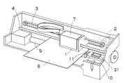
図1中符号1はキャリッジであり、このキャリッジ1はキャリッジモータ2により駆動されるタイミングベルト3を介し、ガイド部材4に案内されてプラテン5の軸方向に往復移動されるように構成されている。
【0031】
キャリッジ1の記録用紙6に対向する側にはインクジェット式記録ヘッドが搭載され、またその上部には記録ヘッドにインクを供給するインクカートリッジ7が着脱可能に装着されている。
【0032】
この記録装置の非印字領域であるホームポジション(図中、右側)にはキャップ部材31が配置されており、このキャップ部材31はキャリッジ1に搭載された記録ヘッドがホームポジションに移動した時に、記録ヘッドのノズル形成面に押し当てられてノズル形成面との間に密閉空間を形成するように構成されている。そして、キャップ部材31の下方には、キャップ部材31により形成された密閉空間に負圧を与えてクリーニング等を実施するためのポンプユニット10が配置されている。
【0033】
そして、キャップ部材31における印字領域側の近傍には、ゴムなどの弾性板を備えたワイピング手段11が記録ヘッドの移動軌跡に対して例えば水平方向に進退できるように配置されていて、キャリッジ1がキャップ部材31側に往復移動するに際して、必要に応じて記録ヘッドのノズル形成面を払拭することができるように構成されている。
【0034】
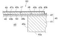
図2及び図3は、本実施形態による圧電装置を示した図であり、この圧電装置60は、基板41に振動板42を積層して構成された基部40を有し、この基部40は、互いに対向する第1面40a及び第2面40bを有する。基部40には、検出対象の媒体を受け入れるための円形のキャビティ43が、第1面40a側に開口するようにして形成されており、キャビティ43の底面部43bが振動板42にて振動可能に形成されている。基部40の第2面40b側の両端には下部電極端子44及び上部電極端子45が形成されている。
【0035】
基部40の第2面40bには下部電極層(第1電極層)46が形成されており、この下部電極層46は、キャビティ43に対応する領域の中に形成された本体部46aと、この本体部46aからキャビティ43の周縁43aに対応する位置を越えて延びる延出部46bと、を有する。下部電極層46の本体部46aは円形を成しており、その中心はキャビティ43の中心とほぼ一致している。下部電極層46の本体部46aはキャビティ43よりも小径に構成されている。
【0036】
下部電極層46の上には圧電層47が積層されており、この圧電層47は、キャビティ43に対応する領域の中に形成された本体部47aと、この本体部47aからキャビティ43の周縁43aに対応する位置を越えて延びる延出部47bと、を有する。圧電層47の本体部47aは円形を成しており、その中心はキャビティ43の中心とほぼ一致している。圧電層47の本体部47aは、キャビティ43よりも小径に、且つ、下部電極層46の本体部46aよりも大径に形成されている。
【0037】
基部40の第2面40b側には補助電極層48が形成されており、この補助電極層48は、好ましくは、下部電極層46と同じ材質で且つ同じ厚さである。補助電極層48の一部が第2面40bと圧電層47の延出部47bとの間に位置しており、圧電層47の延出部47bを下方から支持している。このように補助電極層48の一部によって圧電層47の延出部47bを支持することによって、圧電層47に段差が生じることを防止している。
【0038】
圧電層47には上部電極層(第2電極層)49が積層されており、この上部電極層49は、圧電層47の本体部47a上に形成された本体部49aと、この本体部49aからキャビティ43の周縁43aに対応する位置を越えて延びる延出部49bと、を有する。上部電極層49の延出部49bは補助電極層48に接続されており、補助電極層48を介して上部電極層49と上部電極端子45とが電気的に接続されている。このように補助電極層48を介して上部電極層49を上部電極端子45に接続することによって、圧電層47及び下部電極層46の合計の厚さから生じる段差を、上部電極層49と補助電極層48との両方によって吸収することができる。このため、上部電極層49に大きな段差が生じて機械的強度が低下することを防止することができる。
【0039】
上部電極層49の本体部49aは円形を成しており、その中心はキャビティ43の中心とほぼ一致している。上部電極層49の本体部49aは、圧電層47の本体部47a及びキャビティ43よりも小径に、且つ、下部電極層46の本体部46aよりも大径に形成されている。
【0040】
このように、圧電層47の本体部47aは、上部電極層49の本体部49aと下部電極層46の本体部46aとによって挟みこまれる構造となっている。これにより、圧電層47は効果的に変形駆動され得る。
【0041】
上述のように、上部電極層49の本体部49a、圧電層47の本体部47a、下部電極層46の本体部46aおよびキャビティ43のうちで、面積が最も大きいのはキャビティ43である。このような構造のために、振動板42のうち実際に振動する振動領域は、キャビティ43によって決定される。
【0042】
また、上部電極層49の本体部49a、圧電層47の本体部47aおよび下部電極層46の本体部46aの各面積が、キャビティ43の面積より小さいことにより、振動板42がより振動しやすくなっている。
【0043】
さらに、圧電層47と電気的に接続された下部電極層46の本体部46aおよび上部電極層49の本体部49aのうち、下部電極層46の本体部46aの方が小さい。従って、下部電極層46の本体部46aが、圧電層47のうちで圧電効果を発生する部分を決定する。
【0044】
圧電層47の本体部47a、上部電極層49の本体部49a、及び下部電極層46の本体部46aは、それらの中心が、キャビティ43の中心とほぼ一致している。また、振動板42の振動部分を決定する円形状のキャビティ43の中心は、圧電装置60の全体のほぼ中心に位置している。したがって、圧電装置60の振動部の中心は、圧電装置60の中心とほぼ一致する。
【0045】
更に、圧電層47の本体部47a、上部電極層49の本体部49a、下部電極層46の本体部46a、及び振動板42の振動部分が円形形状を有するので、圧電装置60の振動部は、圧電装置60の中心に対して対称な形状である。このように圧電装置60の振動部が、圧電装置60の中心に対して対称な形状であるので、構造の非対称性から生じ得る不要な振動を励起することがない。このため、共振周波数の検出精度が向上する。
【0046】
また、圧電装置60の振動部が等方的な形状であるので、圧電装置60を接着する際に固定のばらつきの影響を受けにくく、インク容器に均等に接着され得る。すなわち、圧電装置60のインク容器への実装性がよい。
【0047】
更に、振動板42のコンプライアンスが大きいので、振動の減衰が小さくなり、共振周波数の検出の精度が向上できる。
【0048】
圧電装置60に含まれる部材は、互いに焼成されることによって一体的に形成されていることが好ましい。圧電装置60を一体的に形成することによって、圧電装置60の取り扱いが容易になる。
【0049】
さらに、基板41の強度を高めることによって、振動特性が向上し得る。即ち、基板41の強度を高めることによって、圧電装置60の振動部のみが振動し、圧電装置60のうち振動部以外の部分が振動しないようになる。また、振動部の振動を大きくするためには、基板41の強度を高めることに加えて、圧電装置60の圧電層47、上部電極層49、及び下部電極層46を薄くかつ小さくすると共に、振動板41を薄くすることが有効である。
【0050】
圧電層47の材料としては、ジルコン酸チタン酸鉛(PZT)、ジルコン酸チタン酸鉛ランタン(PLZT)、または、鉛を使用しない鉛レス圧電膜、を用いることが好ましい。基板41の材料としては、ジルコニアまたはアルミナを用いることが好ましい。また、振動板42には、基板41と同じ材料を用いることが好ましい。上部電極層49、下部電極層46、上部電極端子45および下部電極端子44は、導電性を有する材料、例えば、金、銀、銅、プラチナ、アルミニウム、ニッケルなどの金属を用いることができる。
【0051】
図3に示したように、下部電極層46と補助電極層48との間には絶縁用空隙50が形成されている。そして、この絶縁用空隙50は、キャビティ43の周縁43aに対応する位置を外して形成されており、より具体的には、絶縁用空隙50はその全体がキャビティ43に対応する領域の中に位置するようにして形成されている。
【0052】
このように、絶縁用空隙50の全体をキャビティ43に対応する領域の中に位置させることによって、圧電装置60の駆動によってその振動部を振動させた際に、キャビティ43の周縁43aに対応する位置において圧電層47に発生する応力集中を大幅に抑制することができる。このため、圧電層47及び上部電極層49におけるクラックの発生を防止することができる。
【0053】
また、補助電極層48は、キャビティ43の周縁43aに対応する位置を越えて、キャビティ43に対応する領域の外側から内側に向けて突出する突出部48aを有しており、この突出部48aはその角が丸められている。
【0054】
このように補助電極層48の突出部48aの角を丸めることによって、補助電極層48のエッジ部分における圧電層47のクラックの発生を防止することができる。さらに、補助電極層48の形成時に位置ずれが発生する場合を考慮すると、補助電極層48の突出部48aに角が存在すると、形成時の位置ずれによって突出部48aの角がキャビティ43に対応する領域の内側に入ったり外側に外れたりする。このため、圧電装置60ごとの振動特性にバラツキが生じてしまう恐れがある。これに対して、本実施形態のように補助電極層48の突出部48aの角を丸めることによって、補助電極層48の形成時の位置ずれに起因する振動特性のバラツキを大幅に抑制することができる。
【0055】
図4は、本実施形態において用いられる圧電装置60およびその等価回路を示す。この圧電装置60は、残留振動による共振周波数を検出することで音響インピーダンスの変化を検知して、インクカートリッジ内の液体の消費状態を検出するものである。
【0056】
図4(A)および図4(B)は、圧電装置60の等価回路を示す。また、図4(C)および図4(D)は、それぞれインクカートリッジ内にインクが満たされているときの圧電装置60を含む周辺およびその等価回路を示し、図4(E)および図4(F)は、それぞれインクカートリッジ内にインクが無いときの圧電装置60を含む周辺およびその等価回路を示す。
【0057】
図2乃至図4に示される圧電装置60は、インクカートリッジ7のインク容器の所定の場所に、キャビティ43がインク容器内に収容される液体(インク)と接触するように装着される。つまり、圧電装置60の振動部の少なくとも一部が、インク容器の収容空間に露出している。インク容器に液体が十分に収容されている場合には、キャビティ43内およびその外側は液体によって満たされている。
【0058】
一方、インク容器の液体が消費され、圧電装置の装着位置以下まで液面が降下すると、キャビティ43内に液体が存在しない状態となる、あるいは、キャビティ43内にのみ液体が残存されその外側には気体が存在する状態となる。
【0059】
圧電装置60は、この状態の変化に起因する音響インピーダンスの相違を検出する。それによって、圧電装置60は、インク容器に液体が十分に収容されている状態であるか、あるいは、ある一定以上の液体が消費された状態であるか、を検知することができる。
【0060】
次に、圧電装置による液面検出の原理について説明する。
圧電装置60は、液体の音響インピーダンスの変化を共振周波数の変化を用いて検出することができる。共振周波数は、圧電装置の振動部が振動した後に振動部に残留する残留振動によって生ずる逆起電力を測定することによって検出することができる。すなわち、圧電装置60の圧電層47は、圧電装置60の振動部に残留する残留振動により逆起電力を発生する。逆起電力の大きさは、圧電装置60の振動部の振幅によって変化する。従って、圧電装置60の振動部の振幅が大きいほど、検出が容易である。
【0061】
また、圧電装置60の振動部における残留振動の周波数によって、逆起電力の大きさが変化する周期が変わる。すなわち、圧電装置60の振動部の周波数は、逆起電力の周波数に対応する。ここで、共振周波数は、圧電装置60の振動部と振動部に接する媒体との共振状態における周波数をいう。
【0062】
圧電装置60の振動領域は、振動板42のうちのキャビティ43に対応する部分である。インク容器内に液体が充分に収容されている場合には、キャビティ43内には、液体が満たされ、振動領域はインク容器内の液体と接触している。一方で、インク容器内に液体が充分にない場合には、振動領域はインク容器内のキャビティ43に残った液体と接するか、あるいは、液体と接触せず、気体または真空と接触する。
【0063】
ここで、図2乃至図4を参照しながら、逆起電力の測定により得られる媒体と圧電装置60の振動部との共振周波数から、インク容器内の液体の状態を検出する動作および原理について説明する。
【0064】
圧電装置60において、上部電極端子45および下部電極端子44を介して、それぞれ上部電極層49および下部電極層46に電圧を印加する。すると、圧電層47のうち、上部電極層49および下部電極層46に挟まれた部分に電界が生じる。この電界によって、圧電層47は変形する。圧電層47が変形することによって、振動板42のうちの振動領域がたわみ振動する。圧電層47が変形した後しばらくは、たわみ振動が圧電装置60の振動部に残留する。
【0065】
残留振動は、圧電装置60の振動部と媒体との自由振動である。従って、圧電層47に印加する電圧をパルス波形あるいは矩形波とすることで、電圧を印加した後の振動部と媒体との共振状態を容易に得ることができる。残留振動は、圧電装置60の振動部の振動であり、圧電層47の変形を伴う。このため、圧電層47は逆起電力を発生する。この逆起電力は、上部電極層49、下部電極層46、上部電極端子45および下部電極端子44を介して検出される。検出された逆起電力によって、共振周波数が特定できる。この共振周波数に基いて、インク容器内の液体の有無を検出することができる。
【0066】
一般に、共振周波数fsは、
fs=1/(2*π*(M*Cact)1/2) (式1)
で表される。ここで、Mは振動部のイナータンスMactと付加イナータンスM’との和である。Cactは振動部のコンプライアンスである。
【0067】
図4(A)および図4(B)は、キャビティ43にインクが残存していないときの圧電装置60の振動部およびキャビティ43の等価回路である。
【0068】
Mactは、振動部の厚さと振動部の密度との積を振動部の面積で除したものであり、詳細には、図4(A)に示すように、
Mact=Mpzt+Melectrode1+Melectrode2+Mvib (式2)
と表される。
【0069】
ここで、Mpztは、振動部における圧電層47の厚さと圧電層47の密度との積を圧電層47の面積で除したものである。Melectrode1は、振動部における上部電極層49の厚さと上部電極層49の密度との積を上部電極層49の面積で除したものである。Melectrode2は、振動部における下部電極層46の厚さと下部電極層46の密度との積を下部電極層46の面積で除したものである。Mvibは、振動部における振動板42の厚さと振動板42の密度との積を振動板42の振動領域の面積で除したものである。
【0070】
ただし、Mactを振動部全体としての厚さ、密度および面積から算出することができるように、圧電層47、上部電極層49、下部電極層46および振動板42の振動領域のそれぞれの面積は、上述のような大小関係を有するものの、相互の面積の差は微小であることが好ましい。
【0071】
また、本実施形態において、圧電層47、上部電極層49および下部電極層46においては、それらの主要部である円形の本体部47a、49a、46a以外の部分は、主要部に対して無視できるほど微小であることが好ましい。従って、圧電装置60において、Mactは、上部電極層49、下部電極層46、圧電層47および振動板42のうちの振動領域のそれぞれのイナータンスの和である。また、コンプライアンスCactは、上部電極層49、下部電極層46、圧電層47および振動板42のうちの振動領域によって形成される部分のコンプライアンスである。
【0072】
尚、図4(A)、(B)、(D)、(F)は、圧電装置60の振動部およびキャビティ43の等価回路を示すが、これらの等価回路において、Cactは圧電装置60の振動部のコンプライアンスを示す。Cpzt、Celectrode1、Celectrode2およびCvibは、それぞれ、振動部における圧電層47、上部電極層49、下部電極層46および振動板42のコンプライアンスを示す。Cactは、以下の式3で表される。
1/Cact=(1/Cpzt)+(1/Celectrode1)+(1/Celectrode2)
+(1/Cvib) (式3)
式2および式3より、図4(A)は、図4(B)のように表すこともできる。
【0073】
コンプライアンスCactは、単位面積に圧力をかけたときの変形によって受容できる媒体の体積を表す。すなわち、コンプライアンスCactは、変形のし易さを表す。
【0074】
図4(C)は、インク容器に液体が十分に収容され、圧電装置60の振動領域の周辺に液体が満たされている場合の圧電装置60の断面図を示す。図4(C)のM’maxは、インク容器に液体が十分に収容され、圧電装置60の振動領域の周辺に液体が満たされている場合の付加イナータンス(付加質量(振動領域の振動に影響を及ぼす質量)を面積の2乗で除したもの)の最大値を表す。M’maxは、
M’max=(π*ρ/(2*k3))*(2*(2*k*a)3/(3*π))/(π*a2)2 (式4)
(aは振動部の半径、ρは媒体の密度、kは波数である。)
で表される。
【0075】
尚、式4は、圧電装置60の振動領域が半径aの円形である場合に成立する。付加イナータンスM’は、振動部の付近にある媒体によって、振動部の質量が見かけ上増加していることを示す量である。式4からわかるように、M’maxは、振動部の半径aと媒体の密度ρとによって、大きく変化する。
【0076】
波数k は、
k=2*π*fact/c (式5)
(factは、振動部の共振周波数である。cは、媒体中を伝播する音響の速度である。)
で表される。
【0077】
図4(D)は、インク容器に液体が十分に収容され、圧電装置60の振動領域の周辺に液体が満たされている図4(C)の場合の圧電装置60の振動部およびキャビティ43の等価回路を示す。
【0078】
図4(E)は、インク容器の液体が消費され、圧電装置60の振動領域の周辺に液体が無いものの、圧電装置60のキャビティ43内には液体が残存している場合の圧電装置60の断面図を示す。
【0079】
式4は、インク容器に液体が満たされている場合に、インクの密度ρなどから決定される最大のイナータンスM’maxを表す式である。一方、インク容器内の液体が消費され、キャビティ43内に液体が残留しつつ圧電装置60の振動領域の周辺にある液体が気体または真空に置換された場合等の付加イナータンスM’は、一般的に、
M’=ρ*t/S (式6)
と表せる(より詳しくは、後述の式8参照)。ここで、tは振動にかかわる媒体の厚さである。Sは、圧電装置60の振動領域の面積である。振動領域が半径aの円形の場合は、S=π*a2である。
【0080】
従って、付加イナータンスM’は、インク容器に液体が十分に収容され、圧電装置60の振動領域の周辺に液体が満たされている場合には、式4に従う。一方で、液体が消費され、キャビティ43内に液体が残留しつつ圧電装置60の振動領域の周辺にある液体が気体または真空に置換された場合には、式6に従う。
【0081】
ここで、図4(E)のように、インク容器の液体が消費され、圧電装置60の振動領域の周辺に液体が無いものの、圧電装置60のキャビティ43内には液体が残存している場合の付加イナータンスM’を、便宜的にM’cavとし、圧電装置60の振動領域の周辺に液体が満たされている場合の付加イナータンスM’maxと区別する。
【0082】
図4(F)は、インク容器の液体が消費され、圧電装置60の振動領域の周辺に液体が無いものの、圧電装置60のキャビティ43内には液体が残存している図4(E)の場合の圧電装置60の振動部およびキャビティ43の等価回路を示す。
【0083】
ここで、媒体の状態に関係するパラメータは、式6において、媒体の密度ρおよび媒体の厚さtである。インク容器内に液体が充分に収容されている場合は、圧電装置60の振動部に液体が接触する。一方、インク容器内に液体が充分に収容されていない場合は、キャビティ43内部に液体が残存するか、もしくは、圧電装置60の振動部に気体または真空が接触する。圧電装置60の周辺の液体が消費され、図4(C)のM’maxから図4(E)のM’cavへ移行する過程における付加イナータンスM’varは、インク容器内の液体の収容状態によって媒体の密度ρや媒体の厚さtが変化することに伴って変化する。これにより、共振周波数fsも変化する。従って、共振周波数fsを特定することによって、インク容器内の液体の量を検出することができる。
【0084】
ここで、図4(E)に示すようにt=dとした場合、式6を用いてM’cavを表すと、式6のtにキャビティの深さdを代入し、
M’cav=ρ*d/S (式7)
となる。
【0085】
また、媒体が互いに種類の異なる液体であれば、組成の違いによって密度ρが異なるため、付加イナータンスM´及び共振周波数fsが異なる。従って、共振周波数fsを特定することで、液体の種類を検出できる。
【0086】
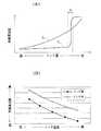
図5(A)は、インクタンク内のインクの量とインクおよび振動部の共振周波数fsとの関係を示すグラフである。ここでは液体の1例としてインクについて説明する。縦軸は、共振周波数fsを示し、横軸は、インク量を示す。インク組成が一定であるとき、インク残量の低下に伴い、共振周波数fsは、上昇する。
【0087】
インク容器にインクが十分に収容され、圧電装置60の振動領域の周辺にインクが満たされている場合には、その最大付加イナータンスM’maxは、式4に表わされる値となる。一方で、インクが消費され、キャビティ43内にインクが残留しつつ圧電装置60の振動領域の周辺にインクが満たされていないときには、付加イナータンスM’var は、媒体の厚さtに基づいて式6によって算出される。式6中のtは、振動にかかわる媒体の厚さであるから、インクが残留する圧電装置60のキャビティ43の深さdを小さく、即ち、基板41の厚さを十分に薄くすることによって、インクが徐々に消費されていく過程を検出することもできる(図4(C)参照)。ここで、tinkは振動にかかわるインクの厚さとし、tink−maxはM’maxにおけるtinkとする。
【0088】
例えば、圧電装置60は、インクカートリッジの底面にインクの液面に対してほぼ水平に配置される。この場合、インクが消費され、インクの液面が圧電装置60からtink-maxの高さ以下になると、式6によりM’varが徐々に変化し、式1により共振周波数fsが徐々に変化する。従って、インクの液面がtの範囲内にある限り、圧電装置60はインクの消費状態を徐々に検出することができる。
【0089】
あるいは、インクカートリッジの側壁に、圧電装置60はインクの液面に対してほぼ垂直に配備され得る。この場合、インクが消費され、インクの液面が圧電装置60の振動領域に達すると、水位の低下に伴い付加イナータンスM’が減少する。これにより、式1により共振周波数fsが徐々に増加する。従って、インクの液面がキャビティ43の直径2a(図4(C)参照)の範囲内にある限り、圧電装置60はインクの消費状態を徐々に検出することができる。
【0090】
図5(A)の曲線Xは、底面に配置された圧電装置60のキャビティ43を十分に浅くした場合や、側壁に配置された圧電装置60の振動領域を十分に大きくまたは長くした場合の、インクタンク内に収容されたインクの量とインクおよび振動部の共振周波数fsとの関係を表わしている。インクタンク内のインクの量が減少するとともに、インクおよび振動部の共振周波数fsが徐々に変化していく様子が理解できる。
【0091】
より詳細には、インクが徐々に消費されていく過程を検出することができる場合とは、圧電装置60の振動領域の周辺において、互いに密度が異なる液体と気体とがともに存在しかつ振動にかかわる場合である。インクが徐々に消費されていくに従って、圧電装置60の振動領域周辺において振動にかかわる媒体は、液体が減少する一方で気体が増加する。
【0092】
例えば、圧電装置60をインクの液面に対して水平に配備した場合であって、tink がtink−maxより小さいときには、圧電装置60の振動にかかわる媒体はインクと気体との両方を含む。したがって、圧電装置60の振動領域の面積Sを用いて、式4のM’max以下になった状態をインクと気体の付加質量で表すと、
M’=M’air+M’ink= ρair*tair/S+ρink*tink/S (式8)
となる。ここで、M’airは空気のイナータンスであり、M’inkはインクのイナータンスである。ρairは空気の密度であり、ρinkはインクの密度である。tairは振動にかかわる空気の厚さであり、tinkは振動にかかわるインクの厚さである。
【0093】
圧電装置60の振動領域周辺における振動にかかわる媒体のうち、液体が減少して気体が増加するに従い、圧電装置60がインクの液面に対しほぼ水平に配備されている場合には、tairが増加し、tinkが減少する。それによって、M’varが徐々に減少し、共振周波数が徐々に増加する。よって、インクタンク内に残存しているインクの量またはインクの消費量を検出することができる。尚、式7において液体の密度のみの式となっているのは、液体の密度に対して、空気の密度が無視できるほど小さい場合を想定しているからである。
【0094】
圧電装置60がインクの液面に対しほぼ垂直に配備されている場合には、圧電装置60の振動領域のうち、圧電装置60の振動にかかわる媒体がインクのみの領域と、圧電装置60の振動にかかわる媒体が気体のみの領域との並列の等価回路(図示せず)と考えられる。圧電装置60の振動にかかわる媒体がインクのみの領域の面積をSinkとし、圧電装置60の振動にかかわる媒体が気体のみの領域の面積をSairとすると、
1/M’=1/M’air+1/M’ink=Sair/(ρair*tair)+Sink/(ρink*tink)(式9)
となる。
【0095】
尚、式9は、圧電装置60のキャビティ43にインクが保持されない場合に適用される。圧電装置60のキャビティ43にインクが保持される場合の付加イナータンスについては、式9によるM’と式7のM’cav との和によって計算することができる。
【0096】
圧電装置60の振動は、tink−maxの深さからインクの残留する深さdまで変化するので、インクの残留する深さがtink−maxよりわずかに小さい程度で圧電装置60が底面に配置されている場合には、インクが徐々に減少する過程を検出することは出来ない。この場合、tink−maxから残留する深さdまでのわずかなインク量変化における圧電装置の振動変化から、インク量が変化したことを検出する。また、側面に配置され、キャビティ43の径が小さい場合は、キャビティ43を通過する間の圧電装置60の振動変化は微量なので、通過過程のインク量を検出することは難しく、インク液面がキャビティ43より上か下かを検出する。
【0097】
例えば、図5(A)の曲線Yは、小さい円形の振動領域の場合におけるインクタンク内のインクの量とインクおよび振動部の共振周波数fsとの関係を示す。インクタンク内のインクの液面が圧電装置60の装着位置を通過する前後におけるインク量の差Qの間で、インクおよび振動部の共振周波数fsが激しく変化している様子が示される。このことから、インクタンク内にインクが所定量残存しているか否かを2値的に検出することができる。
【0098】
圧電装置60を用いて液体の有無を検出する方法は、振動板42が液体と直接接触することでインクの有無を検出するので、インクの消費量をソフトウェアによって計算する方法に比べ、検出精度が高い。更に、電極を用いて導電性によりインクの有無を検出する方法は、インク容器への電極の取付位置及びインクの種類によって影響され得るが、圧電装置60を用いて液体の有無を検出する方法は、インク容器への圧電装置60の取付位置及びインクの種類によって影響され難い。
【0099】
更に、単一の圧電装置60を用いて発振と液体の有無の検出との双方を実施することができるので、発振と液体の有無の検出とを異なったセンサを用いて実施する方法と比較して、インク容器に取付けるセンサの数を減少することができる。したがって、液量検出機能を持つインク容器を安価に製造できる。なお、圧電層47の振動周波数を非可聴領域に設定することで、圧電装置60の動作中に発生する音を静かにすることが好ましい。
【0100】
図5(B)は、インクの密度とインクおよび振動部の共振周波数fsとの関係の一例を示す。ここでは、液体の例としてインクについて説明しており、「インク満」と「インク空」(或いは「インク無し」)とは相対的な2状態を意味し、いわゆるインクフル状態とインクエンド状態とを意味するものではない。図5(B)に示すように、インク密度が高い場合、付加イナータンスが大きくなるので共振周波数fsが低下する。すなわち、インクの種類によって共振周波数fsが異なる。したがって、共振周波数fsを測定することによって、インクを再充填する際に、密度の異なったインクが混入されていないか確認することができる。つまり、互いに種類の異なるインクを収容するインクタンクを識別できる。
【0101】
続いて、インク容器内の液体が空の状態であっても圧電装置60のキャビティ43内に液体が残存するようにキャビティ43のサイズと形状を設定した時において、液体の状態を正確に検出できる条件を詳述する。圧電装置60は、キャビティ43内に液体が満たされている場合に液体の状態を検出できれば、キャビティ43内に液体が満たされていない場合であっても液体の状態を検出できる。
【0102】
共振周波数fsは、イナータンスMの関数である。イナータンスMは、振動部のイナータンスMactと付加イナータンスM’との和である。ここで、付加イナータンスM’が液体の状態と関係する。付加イナータンスM’は、振動部の付近にある媒体によって振動部の質量が見かけ上増加していることを示す量である。即ち、振動部の振動によって見かけ上媒体を吸収する(振動に関わるイナータンスが増加する)ことによる振動部の質量の増加分をいう。
【0103】
従って、M’cav が式4におけるM’max よりも大きい場合には、見かけ上吸収する媒体は全てキャビティ43内に残存する液体である。よって、インク容器内に液体が満たされている状態と同じである。この場合、振動に関わる媒体はM’max よりも小さくならないので、インクが消費されても変化を検出することが出来ない。
【0104】
一方、M’cavが式4におけるM’ maxよりも小さい場合には、見かけ上吸収する媒体はキャビティ43内に残存する液体およびインク容器内の気体または真空である。このときにはインク容器内に液体が満たされている状態とは異なりM’が変化するので、共振周波数fsが変化する。従って、圧電装置60は、インク容器内の液体の状態を検出できる。
【0105】
即ち、インク容器内の液体が空の状態で、圧電装置60のキャビティ43内に液体が残存する場合に、圧電装置60が液体の状態を正確に検出できる条件は、M’cavがM’maxよりも小さいことである。尚、圧電装置60が液体の状態を正確に検出できる条件M’max>M’cavは、キャビティ43の形状にかかわらない。
【0106】
ここで、M’cav は、キャビティ43の容量とほぼ等しい容量の液体の質量イナータンスである。従って、M’max >M’cav の不等式から、圧電装置60が液体の状態を正確に検出できる条件は、キャビティ43の容量の条件として表すことができる。例えば、円形状のキャビティ43の半径をaとし、およびキャビティ43の深さをdとすると、
M’max>ρ*d/πa2 (式10)
である。式10を展開すると
a/d>3*π/8 (式11)
という条件が求められる。従って、式11を満たす開口161の半径aおよびキャビティ43の深さdであるキャビティ43を有する圧電装置60であれば、インク容器内の液体が空の状態であって、かつ、キャビティ43内に液体が残存する場合であっても、誤作動することなく液体の状態を検出できる。
【0107】
尚、式10、式11は、キャビティ43の形状が円形の場合に限り成立する。キャビティ43の形状が円形でない場合、対応するM’maxの式を用い、式10中のπa2をその面積と置き換えて計算すれば、キャビティ43の幅および長さ等のディメンジョンと深さの関係が導き出せる。
【0108】
なお、付加イナータンスM’は音響インピーダンス特性にも影響するので、残留振動により圧電装置60に発生する逆起電力を測定する方法は、少なくとも音響インピーダンスの変化を検出しているともいえる。
【0109】
図6(A) および図6(B)は、圧電装置60に駆動信号を供給して振動部を振動させた後の、圧電装置60の残留振動の波形と残留振動の測定方法とを示す。インクカートリッジ内の圧電装置60の装着位置レベルにおけるインク液位の上下は、圧電装置60が発振した後の残留振動の周波数変化や、振幅の変化によって検出することができる。図6(A) および図6(B)において、縦軸は圧電装置60の残留振動によって発生した逆起電力の電圧を示し、横軸は時間を示す。圧電装置60の残留振動によって、図6(A) および図6(B)に示すように電圧のアナログ信号の波形が発生する。次に、アナログ信号を、信号の周波数に対応するデジタル数値に変換(二値化)する。図6(A)および図6(B)に示した例においては、アナログ信号の4パルス目から8パルス目までの4個のパルスが生じる時間を計測している。
【0110】
より詳細には、圧電装置60が発振した後、予め設定された所定の基準電圧を低電圧側から高電圧側へ横切る回数をカウントする。そして、4カウントから8カウントまでの間をHighとしたデジタル信号を生成し、所定のクロックパルスによって4カウントから8カウントまでの時間を計測する。
【0111】
図6(A)は、圧電装置60の装着位置レベルよりも上位にインク液面があるときの波形である。一方、図6(B)は圧電装置60の装着位置レベルにおいてインクが無いときの波形である。図6(A)と図6(B)とを比較すると、図6(A)の方が図6(B)よりも4カウントから8カウントまでの時間が長いことがわかる。換言すると、インクの有無によって4カウントから8カウントまでの所要時間が異なる。この所要時間の相違を利用して、インクの消費状態を検出することができる。
【0112】
アナログ波形の4カウント目から数えるのは、圧電装置60の振動が安定してから計測をはじめるためである。4カウント目からとしたのは単なる一例であって、任意のカウントから数えてもよい。ここでは、4カウント目から8カウント目までの信号を検出し、所定のクロックパルスによって4カウント目から8カウント目までの時間を測定している。この時間に基いて、共振周波数を求めることができる。クロックパルスは、8カウント目までの時間を測定する必要は無く、任意のカウントまで数えてもよい。図6においては、4カウント目から8カウント目までの時間を測定しているが、周波数を検出する回路構成にしたがって、異なったカウント間隔内の時間を検出してもよい。
【0113】
例えば、インクの品質が安定していてピークの振幅の変動が小さい場合には、検出の速度を上げるために4カウント目から6カウント目までの時間を検出することにより共振周波数を求めてもよい。また、インクの品質が不安定でパルスの振幅の変動が大きい場合には、残留振動を正確に検出するために4カウント目から12カウント目までの時間を検出してもよい。
【0114】
図7は、圧電装置60を取付モジュール体100として一体形成した構成を示す斜視図である。モジュール体100は、インクカートリッジのインク容器の所定個所に装着される。モジュール体100は、インク容器内の媒体の少なくとも音響インピーダンスの変化を検出することにより、インク容器内の液体の消費状態を検知するように構成されている。
【0115】
本実施形態のモジュール体100は、インク容器に圧電装置60を取り付けるためのインク容器取付部101を有する。インク容器取付部101は、平面がほぼ矩形の基台102と、駆動信号により発振する圧電装置60を収容する基台102上の円柱部116と、を有している。また、モジュール体100は、インクカートリッジに装着されたときに、モジュール体100の圧電装置60が外部から接触できないように構成されている。これにより、圧電装置60を外部の接触から保護することができる。なお、円柱部116の先端側エッジは丸みが付けられていて、インクカートリッジに形成された孔へ装着する際に嵌めやすくなっている。
【0116】
図8は、図7に示したモジュール体100の分解図である。モジュール体100は、樹脂からなるインク容器取付部101と、プレート110および凹部113を有する圧電装置装着部105(図7参照)とを含む。さらに、モジュール体100は、リードワイヤ104a及び104b、圧電装置60及びフィルム108を有する。好ましくは、プレート110は、ステンレス又はステンレス合金等の錆びにくい材料から形成される。
【0117】
インク容器取付部101に含まれる円柱部116および基台102は、リードワイヤ104a及び104bを収容できるように中心部に開口部114が形成されると共に、圧電装置60、フィルム108、及びプレート110を収容できるように開口部114の周囲に凹部113が形成されている。
【0118】
圧電装置60は、プレート110にフィルム108を介して接合され、プレート110および圧電装置60は凹部113(インク容器取付部101)に固定される。従って、リードワイヤ104a及び104b、圧電装置60、フィルム108及びプレート110は、インク容器取付部101に一体として取り付けられる。
【0119】
リードワイヤ104a及び104bは、それぞれ圧電装置60の上部電極端子45及び下部電極端子44と結合して、圧電層47に駆動信号を伝達する一方、圧電装置60が検出した共振周波数の信号を記録装置等へ伝達する。
【0120】
圧電装置60は、リードワイヤ104a及び104bから伝達された駆動信号に基づいて、一時的に発振する。また、圧電装置60は、発振後に残留振動し、その振動によって逆起電力を発生させる。このとき、逆起電力波形の振動周期を検出することによって、インク容器内の液体の消費状態に対応した共振周波数を検出することができる。
【0121】
フィルム108は、圧電装置60とプレート110とを接着して、圧電装置60を液密にする。フィルム108は、ポリオレフィン等によって形成し、熱融着で接着することが好ましい。圧電装置60とプレート110とをフィルム108によって面状に接着して固定することにより、接着の場所によるばらつきが無くなり、振動部以外の部分が振動しない。したがって、圧電装置60をプレート110に接着しても、圧電装置60の振動特性は変化しない。
【0122】
なお、プレート110は円形状であり、基台102の開口部114は円筒状に形成されている。圧電装置60及びフィルム108は矩形状に形成されている。リードワイヤ104a及び104b、圧電装置60、フィルム108及びプレート110は、基台102に対して着脱可能としてもよい。基台102、リードワイヤ104a及び104b、圧電装置60、フィルム108及びプレート110は、モジュール体100の中心軸に対して対称に配置されている。また、基台102、圧電装置60、フィルム108及びプレート110の中心は、モジュール体100のほぼ中心軸上に配置されている。
【0123】
また、基台102の開口部114の面積は、圧電装置60の振動領域の面積よりも大きく形成されている。プレート110の中心で圧電装置60の振動部に直面する位置には、貫通孔112が形成されている。図2乃至図4に示したように、圧電装置60にはキャビティ43が形成されており、貫通孔112とキャビティ43とが、共にインク溜部を形成する。プレート110の厚さは、残留インクの影響を少なくするために、貫通孔112の径に比べて小さいことが好ましい。例えば、貫通孔112の深さはその径の3分の1以下の大きさであることが好ましい。貫通孔112は、モジュール体100の中心軸に対して対称なほぼ真円の形状である。また、貫通孔112の面積は、圧電装置60のキャビティ43の開口面積よりも大きい。貫通孔112の断面の周縁は、テーパ形状であっても良いし、ステップ形状であってもよい。
【0124】
モジュール体100は、貫通孔112がインク容器の内側へ向くように、インク容器の側部、上部又は底部に装着される。インクが消費され、圧電装置60周辺のインクがなくなると、圧電装置60の共振周波数が大きく変化することに基づいて、インクの液位変化を検出することができる。
【0125】
図9は、図7に示したモジュール体100を、インクカートリッジ7のインク容器20に装着したときの、インク容器20の底部近傍の断面図である。モジュール体100は、インク容器20の側壁に形成された貫通孔に装着されている。インク容器20の側壁とモジュール体100との接合面には、Oリング90が設けられ、モジュール体100とインク容器20との液密を保っている。このようにOリング90でシールが出来るために、モジュール体100は、図7で説明したような円柱部を備えることが好ましい。
【0126】
モジュール体100の先端がインク容器20のインク収容空間20aに露出することで、プレート110の貫通孔112を介して、インク容器20内のインクが圧電装置60と接触する。圧電装置60の振動部の周囲が液体か気体かによって、圧電装置60の残留振動の共振周波数が異なるので、モジュール体100を用いてインクの消費状態を検出することができる。
【0127】
次に、図2及び図3に示した実施形態の変形例として、図10に示したように、補助電極層48の突出部48aを、圧電層47の延出部47bよりも幅狭に形成しても良い。
【0128】
このようにすれば、キャビティ43に対応する領域に重なる部分の補助電極層48の面積が小さくなるので、圧電装置60の振動特性を向上させることができる。また、補助電極層48を形成する材料の必要量を減らすことができるので、製造コストを低減することもできる。
【0129】
また、他の変形例としては、図11に示したように、補助電極層48の突出部48aを、圧電層47の延出部47bよりも幅広に形成することもできる。これにより、キャビティ43の周縁部分を補強することができる。
【0130】
さらに、他の変形例としては、図12乃至図14に示したように、下部電極層46、上部電極層49、及び補助電極層48を、全体として、圧電層47の本体部47aの中心を通る対称軸O1、O2を持つような略対称の形状に形成することができる。このように圧電装置60を構成する複数の部材を全体として対称形状に配置することにより、圧電装置60の振動特性を向上させることができる。とりわけ、キャビティ43に対応する領域に位置する部分の下部電極層46、上部電極層49、及び補助電極層48を全体として対称形状にすることにより、圧電装置60の振動特性が向上する。
【0131】
次に、本発明の他の実施形態による圧電装置について図15を参照して説明する。なお、以下では、図2及び図3に示した上記実施形態と異なる部分について説明する。
【0132】
図15に示したように本実施形態による圧電装置70においては、下部電極層46が、キャビティ43に対応する領域の中に位置する円形の本体部46aから、キャビティ43の周縁43aに対応する位置を越えて、補助電極層48に向けて延びる延出部46cを有している。一方、補助電極層48は、その全体が、キャビティ43に対応する領域の外側に形成されている。そして、絶縁用空隙50は、下部電極層46の延出部46cと補助電極層48との間に形成されており、絶縁用空隙50の全体がキャビティ43に対応する領域の外側に位置している。
【0133】
このように絶縁用空隙50の全体をキャビティ43に対応する領域の外側に位置させることによって、圧電装置70の駆動によってその振動部を振動させた際に、キャビティ43の周縁43aに対応する位置において圧電層47に発生する応力集中を大幅に抑制することができる。このため、圧電層47及び上部電極層49におけるクラックの発生を防止することができる。
【0134】
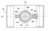
図15に示した実施形態の変形例としては、図16に示したように、下部電極層46、上部電極層49、及び補助電極層48を、全体として、圧電層47の本体部47aの中心を通る対称軸O1、O2を持つような略対称の形状に形成することができる。このように圧電装置70を構成する複数の部材を全体として対称形状に配置することにより、圧電装置70の振動特性を向上させることができる。とりわけ、キャビティ43に対応する領域に位置する部分の下部電極層46、上部電極層49、及び補助電極層48を全体として対称形状にすることにより、圧電装置70の振動特性が向上する。
【0135】
特に、本変形例においては、絶縁用空隙50をキャビティ43に対応する領域の外側に位置させているので、キャビティ43に対応する領域に位置する部分の下部電極層46、上部電極層49、及び補助電極層48の全体としての対称性が高まり、ひいては振動特性のさらなる向上を図ることができる。
【0136】
次に、本発明の他の実施形態としては、上述した各実施形態及び各変形例において、キャビティ43に対応する領域に位置する部分の圧電層47の形状を、圧電層47の本体部47aの中心を通る少なくとも1つの対称軸を持つような略対称の形状とすることができる。より好ましくは、キャビティ43に対応する領域に位置する部分の圧電層47の形状を、圧電層47の延出部47bの延出方向に沿って延びる第1対称軸O1と、第1対称軸O1に直交する第2対称軸O2とを持つような略対称の形状にする。
【0137】
図17は、図14に示した上記例においてその圧電層47の形状を変更した例であり、図18は、図16に示した上記例においてその圧電層47の形状を変更した例を示している。
【0138】
図17及び図18に示した例においては、圧電層47、下部電極層46、上部電極層49、及び補助電極層48を、全体として、圧電層47の本体部47aの中心を通る対称軸O1、O2を持つような略対称の形状に形成している。このように圧電装置60を構成する複数の部材を全体として対称形状に配置することにより、圧電装置60の振動特性を向上させることができる。とりわけ、キャビティ43に対応する領域に位置する部分の圧電層47、下部電極層46、上部電極層49、及び補助電極層48を全体として対称形状にすることにより、圧電装置60の振動特性が向上する。
【0139】
特に、圧電層47は、下部電極層46、上部電極層49、及び補助電極層48に比べて比較的大きな質量を有しているので、圧電層47を対称形状にすることにより振動特性を大幅に向上させることができる。
【0140】
【発明の効果】
本発明によれば、第1電極層と補助電極層との間に形成される絶縁用空隙を、キャビティの周縁に対応する位置を外して形成するようにしたので、圧電装置の駆動によってその振動部を振動させた際に、キャビティの周縁に対応する位置において圧電層に発生する応力集中を大幅に抑制することができる。このため、圧電層及び上部電極層におけるクラックの発生を防止することができる。
【0141】
本発明によれば、キャビティに対応する領域に位置する部分の第1電極層、第2電極層、及び補助電極層を、全体として、圧電層の本体部の中心を通る少なくとも1つの対称軸を持つような略対称の形状を成すように形成したので、圧電装置の振動特性を向上させることができる。
【0142】
本発明によれば、キャビティに対応する領域に位置する部分の圧電層を、圧電層の本体部の中心を通る少なくとも1つの対称軸を持つような略対称の形状を成すように形成したので、圧電装置の振動特性を向上させることができる。
【図面の簡単な説明】
【図1】本発明の一実施形態によるインクカートリッジが使用されるインクジェット式記録装置の概略構成を示した斜視図である。
【図2】本発明の一実施形態における圧電装置を示す図である。
【図3】図2に示した圧電装置の一部を拡大して示した断面図である。
【図4】図2及び図3に示した圧電装置の周辺およびその等価回路を示す図である。
【図5】図2及び図3に示した圧電装置によって検出されるインクの共振周波数とインクの密度との関係を示す図である。
【図6】図2及び図3に示した圧電装置の逆起電力波形を示す図である。
【図7】図2及び図3に示した圧電装置を組み込んだモジュール体を示す斜視図である。
【図8】図7に示したモジュール体の構成を示す分解図である。
【図9】図7に示したモジュール体をインクカートリッジのインク容器に装着した断面の例を示す図である。
【図10】図2及び図3に示した実施形態の一変形例による圧電装置を示した図である。
【図11】図2及び図3に示した実施形態の他の変形例による圧電装置を示した図である。
【図12】図2及び図3に示した実施形態の他の変形例による圧電装置を示した図である。
【図13】図2及び図3に示した実施形態の他の変形例による圧電装置を示した図である。
【図14】図2及び図3に示した実施形態の他の変形例による圧電装置を示した図である。
【図15】本発明の他の実施形態による圧電装置を示した図である。
【図16】図15に示した実施形態の一変形例による圧電装置を示した図である。
【図17】本発明の他の実施形態による圧電装置の一好適例を示した図である。
【図18】本発明の他の実施形態による圧電装置の他の好適例を示した図である。
【図19】従来の圧電装置を示した図である。
【図20】図19に示した従来の圧電装置の一部を拡大して示した断面図である。
【符号の説明】
7 インクカートリッジ
20 インク容器
46 下部電極層
46a 下部電極層の本体部
46b 下部電極層の延出部
47 圧電層
47a 圧電層の本体部
47b 圧電層の延出部
48 補助電極層
48a 補助電極層の突出部
49 上部電極層
49a 上部電極層の本体部
49b 上部電極層の延出部
60、70 圧電装置[0001]
BACKGROUND OF THE INVENTION
The present invention relates to a piezoelectric device and an ink cartridge including the piezoelectric device, and more particularly to a piezoelectric device used for liquid detection and an ink cartridge including the piezoelectric device.
[0002]
[Prior art]
In an ink jet recording apparatus, an ink jet recording head having pressure generating means for pressurizing a pressure generating chamber and a nozzle opening for ejecting the pressurized ink as ink droplets is mounted on a carriage.
[0003]
The ink jet recording apparatus is configured to be able to continue printing by continuously supplying ink in an ink tank (ink container) to a recording head via a flow path. The ink tank is configured as a detachable cartridge that can be easily replaced by the user when ink is consumed, for example.
[0004]
Conventionally, the ink consumption management method of the ink cartridge includes a method of managing the ink consumption by calculating the number of ink droplets ejected from the recording head and the amount of ink sucked by the maintenance by software, or an ink cartridge. There is a method of managing a point in time when a predetermined amount of ink is actually consumed by attaching an electrode for detecting a liquid level.
[0005]
However, the method of managing the ink consumption by calculating the number of ink droplet ejections and the amount of ink by software has the following problems. Some heads have variations in weight of ejected ink droplets. Although the weight variation of the ink droplets does not affect the image quality, the ink cartridge is filled with an amount of ink with a margin in consideration of the accumulation of errors in the ink consumption due to the variation. Therefore, depending on the individual, there is a problem that ink is left by the margin.
[0006]
On the other hand, the method of managing the time when ink is consumed by the electrode can detect the actual amount of ink. For this reason, the remaining amount of ink can be managed with high reliability. However, since the detection of the ink level depends on the conductivity of the ink, the types of ink that can be detected may be limited, and the electrode seal structure may be complicated. In addition, as a material for the electrode, a noble metal having high conductivity and high corrosion resistance is usually used, which increases the manufacturing cost of the ink cartridge. Furthermore, since it is necessary to mount two electrodes, the number of manufacturing steps increases, resulting in an increase in manufacturing cost.
[0007]
In order to solve the above-mentioned problem, Japanese Patent Application No. 2000-147052 describes a piezoelectric device mounted on a liquid container, which can accurately detect the remaining amount of liquid and does not require a complicated sealing structure.
[0008]
According to the technology related to the above-mentioned patent application, the residual generated due to the residual vibration of the vibration part of the piezoelectric device between the case where ink exists in the space facing the vibration part of the piezoelectric device and the case where ink does not exist. The remaining amount of ink in the ink cartridge can be monitored by utilizing the change in the resonance frequency of the vibration signal.
[0009]
[Problems to be solved by the invention]
19 and 20 are diagrams illustrating a conventional piezoelectric device. This piezoelectric device has a
[0010]
An
[0011]
As can be seen from FIG. 20, the
[0012]
However, in the above-described conventional piezoelectric device, when the piezoelectric device is driven to vibrate the vibrating portion, cracks are likely to occur in the
[0013]
The cause of cracking is considered as follows. That is, as shown in FIG. 20, a
[0014]
Further, as can be seen from FIG. 19, in the conventional piezoelectric device, the
[0015]
The present invention has been made in consideration of the above-described circumstances, and provides a piezoelectric device that can prevent the occurrence of cracks in a piezoelectric layer or the like and can improve the vibration characteristics of a vibration part. The purpose is to do.
[0016]
[Means for Solving the Problems]
In order to solve the above problems, a piezoelectric device according to the present invention is a base having a first surface and a second surface facing each other, and a cavity for receiving a medium to be detected is opened on the first surface side. A first portion including a base portion formed so that the bottom surface portion of the cavity can be vibrated, and a main body portion formed on the second surface side and formed in a region corresponding to the cavity. An electrode layer, a piezoelectric layer laminated on the first electrode layer, a main body formed in a region corresponding to the cavity, and a position corresponding to a peripheral edge of the cavity from the main body A piezoelectric layer having an extending portion; and formed on the second surface side of the base portion, and at least a part of the piezoelectric layer is positioned between the second surface and the extending portion to support the extending portion. An auxiliary electrode layer to be laminated on the piezoelectric layer. And a second electrode layer connected to the auxiliary electrode layer, and an insulating gap is provided between the first electrode layer and the auxiliary electrode layer for ensuring an insulating state between the two electrode layers. The insulating gap is formed by removing a position corresponding to a peripheral edge of the cavity.
[0017]
Preferably, the insulating gap is entirely located in a region corresponding to the cavity.
[0018]
Preferably, the auxiliary electrode layer has a protrusion that protrudes inward from the outside of the region corresponding to the cavity beyond the position corresponding to the periphery of the cavity.
[0019]
Preferably, the protrusion of the auxiliary electrode layer has rounded corners.
[0020]
Preferably, the protruding portion of the auxiliary electrode layer is formed wider than the extending portion of the piezoelectric layer.
[0021]
Preferably, the protruding portion of the auxiliary electrode layer is formed narrower than the extending portion of the piezoelectric layer.
[0022]
Preferably, the first electrode layer has an extending portion extending from the inner side of the region corresponding to the cavity to a position corresponding to a peripheral edge of the cavity toward the auxiliary electrode layer, The insulating gap is formed between the extension portion of the first electrode layer and the auxiliary electrode layer, and the entirety thereof is located outside the region corresponding to the cavity.
[0023]
Preferably, a portion of the first electrode layer, the second electrode layer, and the auxiliary electrode layer located in a region corresponding to the cavity has at least the center of the main body portion of the piezoelectric layer as a whole. It has a substantially symmetrical shape with one symmetry axis.
[0024]
Preferably, the portion of the piezoelectric layer located in a region corresponding to the cavity has a substantially symmetrical shape having the at least one axis of symmetry.
[0025]
The piezoelectric device according to the present invention is a base having a first surface and a second surface facing each other, wherein a cavity for receiving a medium to be detected is formed to open to the first surface side, A first electrode layer including a base portion having a bottom surface portion of the cavity formed so as to vibrate; a main body portion formed in a region corresponding to the cavity; and the first electrode layer formed on the second surface side; A piezoelectric layer laminated on the layer, and having a main body formed in a region corresponding to the cavity, and an extending portion extending from the main body beyond a position corresponding to a peripheral edge of the cavity A piezoelectric layer; an auxiliary electrode layer that is formed on the second surface side of the base portion, and at least a part of the piezoelectric layer is positioned between the second surface and the extension portion, and supports the extension portion; and the piezoelectric layer Layered on the auxiliary electrode layer A portion of the first electrode layer, the second electrode layer, and the auxiliary electrode layer located in a region corresponding to the cavity, as a whole, of the piezoelectric layer. It has a substantially symmetrical shape having at least one axis of symmetry passing through the center of the main body.
[0026]
Preferably, the portion of the piezoelectric layer located in a region corresponding to the cavity has a substantially symmetrical shape having the at least one axis of symmetry.
[0027]
The piezoelectric device according to the present invention is a base having a first surface and a second surface facing each other, wherein a cavity for receiving a medium to be detected is formed to open to the first surface side, A first electrode layer including a base portion having a bottom surface portion of the cavity formed so as to vibrate; a main body portion formed in a region corresponding to the cavity; and the first electrode layer formed on the second surface side; A piezoelectric layer laminated on the layer, and having a main body formed in a region corresponding to the cavity, and an extending portion extending from the main body beyond a position corresponding to a peripheral edge of the cavity A piezoelectric layer; an auxiliary electrode layer that is formed on the second surface side of the base portion, and at least a part of the piezoelectric layer is positioned between the second surface and the extension portion, and supports the extension portion; Layered on the auxiliary electrode layer A portion of the piezoelectric layer located in a region corresponding to the cavity has at least one axis of symmetry passing through the center of the body portion of the piezoelectric layer. It is characterized by having the shape of
[0028]
Preferably, the at least one symmetry axis includes a first symmetry axis extending along an extending direction of the extension portion of the piezoelectric layer, and a second symmetry axis perpendicular to the first symmetry axis. .
[0029]
The present invention relates to an ink cartridge for use in an ink jet recording apparatus, comprising: an ink container that stores ink; and any one of the piezoelectric devices described above, wherein the cavity of the piezoelectric device is exposed to an ink storage space of the ink container. It is characterized by that.
[0030]
DETAILED DESCRIPTION OF THE INVENTION
Hereinafter, a piezoelectric device according to an embodiment of the present invention and an ink cartridge including the piezoelectric device will be described with reference to the drawings.
In FIG. 1,
[0031]
An ink jet recording head is mounted on the side of the
[0032]
A
[0033]
A wiping means 11 having an elastic plate such as rubber is disposed in the vicinity of the print area side of the
[0034]
2 and 3 are views showing the piezoelectric device according to the present embodiment. The
[0035]
A lower electrode layer (first electrode layer) 46 is formed on the
[0036]
A
[0037]
An
[0038]
An upper electrode layer (second electrode layer) 49 is laminated on the
[0039]
The
[0040]
As described above, the
[0041]
As described above, the
[0042]
In addition, since the areas of the
[0043]
Furthermore, the
[0044]
The centers of the
[0045]
Further, since the
[0046]
Further, since the vibration part of the
[0047]
Furthermore, since the compliance of the
[0048]
The members included in the
[0049]
Furthermore, the vibration characteristics can be improved by increasing the strength of the
[0050]
As a material of the
[0051]
As shown in FIG. 3, an insulating
[0052]
Thus, by positioning the entire insulating
[0053]
Further, the
[0054]
In this way, by rounding the corners of the
[0055]
FIG. 4 shows a
[0056]
4A and 4B show an equivalent circuit of the
[0057]
The
[0058]
On the other hand, when the liquid in the ink container is consumed and the liquid level drops below the mounting position of the piezoelectric device, the liquid does not exist in the
[0059]
The
[0060]
Next, the principle of liquid level detection using a piezoelectric device will be described.
The
[0061]
Further, the period in which the magnitude of the counter electromotive force changes depends on the frequency of the residual vibration in the vibration part of the
[0062]
The vibration region of the
[0063]
Here, the operation and principle of detecting the state of the liquid in the ink container from the resonance frequency between the medium obtained by measuring the counter electromotive force and the vibration part of the
[0064]
In the
[0065]
The residual vibration is free vibration between the vibration part of the
[0066]
In general, the resonant frequency fs is
fs = 1 / (2 * π * (M * Cact)1/2 (Formula 1)
It is represented by Here, M is the sum of the inertance Mact and the additional inertance M ′ of the vibration part. Cact is the compliance of the vibration part.
[0067]
FIGS. 4A and 4B are equivalent circuits of the vibrating portion of the
[0068]
Mact is obtained by dividing the product of the thickness of the vibration part and the density of the vibration part by the area of the vibration part. Specifically, as shown in FIG.
Mact = Mpzt + Melectrode1 + Melectrode2 + Mvib (Formula 2)
It is expressed.
[0069]
Here, Mpzt is obtained by dividing the product of the thickness of the
[0070]
However, the respective areas of the vibration regions of the
[0071]
In the present embodiment, in the
[0072]
4A, 4 </ b> B, 4 </ b> D, and 4 </ b> F show an equivalent circuit of the vibration unit of the
1 / Cact = (1 / Cpzt) + (1 / Celectrode1) + (1 / Celectrode2)
+ (1 / Cvib) (Formula 3)
From
[0073]
The compliance Cact represents the volume of the medium that can be received by deformation when pressure is applied to the unit area. That is, the compliance Cact represents the ease of deformation.
[0074]
FIG. 4C is a cross-sectional view of the
M'max = (π * ρ / (2 * kThree )) * (2 * (2 * k * a)Three / (3 * π)) / (π * a2 )2 (Formula 4)
(A is the radius of the vibration part, ρ is the density of the medium, and k is the wave number.)
It is represented by
[0075]
[0076]
Wave number k is
k = 2 * π * fact / c (Formula 5)
(Fact is the resonance frequency of the vibration part. C is the speed of sound propagating through the medium.)
It is represented by
[0077]
FIG. 4D shows the vibration portion of the
[0078]
FIG. 4E shows the
[0079]
M ′ = ρ * t / S (Formula 6)
(For more details, see Equation 8 below.) Here, t is the thickness of the medium involved in vibration. S is the area of the vibration region of the
[0080]
Therefore, the additional inertance M ′ follows
[0081]
Here, as shown in FIG. 4E, when the liquid in the ink container is consumed and there is no liquid around the vibration region of the
[0082]
4F shows that the liquid in the ink container is consumed and there is no liquid around the vibration region of the
[0083]
Here, the parameters related to the state of the medium are the density ρ of the medium and the thickness t of the medium in
[0084]
Here, when t = d as shown in FIG. 4 (E), when M′cav is expressed using
M′cav = ρ * d / S (Formula 7)
It becomes.
[0085]
Further, if the medium is a different type of liquid, the density ρ varies depending on the composition, and therefore the additional inertance M ′ and the resonance frequency fs are different. Therefore, the type of liquid can be detected by specifying the resonance frequency fs.
[0086]
FIG. 5A is a graph showing the relationship between the amount of ink in the ink tank and the resonance frequency fs of the ink and the vibration part. Here, ink will be described as an example of liquid. The vertical axis represents the resonance frequency fs, and the horizontal axis represents the ink amount. When the ink composition is constant, the resonance frequency fs increases as the remaining ink amount decreases.
[0087]
When ink is sufficiently contained in the ink container and the ink is filled around the vibration region of the
[0088]
For example, the
[0089]
Alternatively, the
[0090]
A curve X in FIG. 5A is obtained when the
[0091]
More specifically, the case where the process in which ink is gradually consumed can be detected refers to the presence of both liquid and gas having different densities around the vibration region of the
[0092]
For example, when the
M ′ = M′air + M′ink = ρair * tair / S + ρink * tink / S (Formula 8)
It becomes. Here, M′air is an inertance of air, and M′ink is an inertance of ink. ρair is the density of air, and ρink is the density of ink. tair is the thickness of air involved in vibration, and tink is the thickness of ink involved in vibration.
[0093]
Among the media involved in vibration around the vibration region of the
[0094]
In the case where the
1 / M ′ = 1 / M′air + 1 / M′ink = Sair / (ρair * tair) + Sink / (ρink * tink) (Formula 9)
It becomes.
[0095]
Equation 9 is applied when ink is not held in the
[0096]
Since the vibration of the
[0097]
For example, the curve Y in FIG. 5A shows the relationship between the amount of ink in the ink tank and the resonance frequency fs of the ink and the vibration part in the case of a small circular vibration region. A state is shown in which the resonance frequency fs of the ink and the vibration part changes drastically between the difference Q of the ink amount before and after the liquid level of the ink in the ink tank passes through the mounting position of the
[0098]
Since the method of detecting the presence or absence of liquid using the
[0099]
Furthermore, since both oscillation and detection of the presence / absence of liquid can be performed using a single
[0100]
FIG. 5B shows an example of the relationship between the ink density and the resonance frequency fs of the ink and the vibration part. Here, ink is described as an example of a liquid, and “ink full” and “ink empty” (or “no ink”) mean two relative states, so-called ink full state and ink end state. It doesn't mean. As shown in FIG. 5B, when the ink density is high, the additional inertance increases, and therefore the resonance frequency fs decreases. That is, the resonance frequency fs varies depending on the type of ink. Therefore, by measuring the resonance frequency fs, it is possible to confirm whether or not inks having different densities are mixed when refilling the ink. That is, it is possible to identify ink tanks containing different types of ink.
[0101]
Subsequently, when the size and shape of the
[0102]
The resonance frequency fs is a function of the inertance M. The inertance M is the sum of the inertance Mact and the additional inertance M ′ of the vibration part. Here, the additional inertance M ′ is related to the liquid state. The additional inertance M ′ is an amount indicating that the mass of the vibration part is apparently increased by the medium in the vicinity of the vibration part. That is, it means an increase in the mass of the vibration part due to apparent absorption of the medium by the vibration of the vibration part (inertance related to vibration increases).
[0103]
Therefore, when M′cav is larger than M′max in
[0104]
On the other hand, when M′cav is smaller than M′max in
[0105]
That is, when the liquid in the ink container is empty and the liquid remains in the
[0106]
Here, M′cav is the mass inertance of the liquid having a volume approximately equal to the volume of the
M′max> ρ * d / πa2 (Formula 10)
It is. Expanding
a / d> 3 * π / 8 (Formula 11)
This condition is required. Therefore, if the
[0107]
In addition,
[0108]
Note that since the additional inertance M ′ also affects the acoustic impedance characteristics, it can be said that the method of measuring the counter electromotive force generated in the
[0109]
6A and 6B show a residual vibration waveform of the
[0110]
More specifically, after the
[0111]
FIG. 6A shows a waveform when the ink level is higher than the mounting position level of the
[0112]
The reason for counting from the fourth count of the analog waveform is to start measurement after the vibration of the
[0113]
For example, when the ink quality is stable and the fluctuation of the peak amplitude is small, the resonance frequency may be obtained by detecting the time from the 4th count to the 6th count in order to increase the detection speed. . When the ink quality is unstable and the fluctuation of the pulse amplitude is large, the time from the 4th count to the 12th count may be detected in order to accurately detect the residual vibration.
[0114]
FIG. 7 is a perspective view showing a configuration in which the
[0115]
The
[0116]
FIG. 8 is an exploded view of the
[0117]
The
[0118]
The
[0119]
The
[0120]
The
[0121]
The
[0122]
The
[0123]
The area of the
[0124]
The
[0125]
FIG. 9 is a cross-sectional view of the vicinity of the bottom of the
[0126]
When the tip of the
[0127]
Next, as a modification of the embodiment shown in FIGS. 2 and 3, the
[0128]
In this way, the area of the
[0129]
As another modified example, as shown in FIG. 11, the protruding
[0130]
Furthermore, as another modified example, as shown in FIGS. 12 to 14, the
[0131]
Next, a piezoelectric device according to another embodiment of the present invention will be described with reference to FIG. In the following description, parts different from the embodiment shown in FIGS. 2 and 3 will be described.
[0132]
As shown in FIG. 15, in the
[0133]
Thus, by positioning the whole insulating
[0134]
As a modification of the embodiment shown in FIG. 15, as shown in FIG. 16, the
[0135]
In particular, in the present modification, the insulating
[0136]
Next, as another embodiment of the present invention, in each of the above-described embodiments and modifications, the shape of the
[0137]
17 shows an example in which the shape of the
[0138]
In the example shown in FIGS. 17 and 18, the
[0139]
In particular, since the
[0140]
【The invention's effect】
According to the present invention, since the insulating gap formed between the first electrode layer and the auxiliary electrode layer is formed away from the position corresponding to the peripheral edge of the cavity, the vibration is generated by driving the piezoelectric device. When the portion is vibrated, stress concentration generated in the piezoelectric layer at a position corresponding to the peripheral edge of the cavity can be significantly suppressed. For this reason, generation | occurrence | production of the crack in a piezoelectric layer and an upper electrode layer can be prevented.
[0141]
According to the present invention, the portion of the first electrode layer, the second electrode layer, and the auxiliary electrode layer that are located in the region corresponding to the cavity, as a whole, have at least one axis of symmetry passing through the center of the body portion of the piezoelectric layer. The vibration characteristics of the piezoelectric device can be improved because it is formed so as to have a substantially symmetrical shape.
[0142]
According to the present invention, the portion of the piezoelectric layer located in the region corresponding to the cavity is formed to have a substantially symmetrical shape having at least one axis of symmetry passing through the center of the body portion of the piezoelectric layer. The vibration characteristics of the piezoelectric device can be improved.
[Brief description of the drawings]
FIG. 1 is a perspective view showing a schematic configuration of an ink jet recording apparatus in which an ink cartridge according to an embodiment of the present invention is used.
FIG. 2 is a diagram illustrating a piezoelectric device according to an embodiment of the present invention.
3 is an enlarged cross-sectional view showing a part of the piezoelectric device shown in FIG. 2. FIG.
FIG. 4 is a diagram showing the periphery of the piezoelectric device shown in FIGS. 2 and 3 and an equivalent circuit thereof.
5 is a diagram showing a relationship between the resonance frequency of ink detected by the piezoelectric device shown in FIGS. 2 and 3 and the density of ink. FIG.
6 is a diagram showing a back electromotive force waveform of the piezoelectric device shown in FIGS. 2 and 3. FIG.
7 is a perspective view showing a module body incorporating the piezoelectric device shown in FIGS. 2 and 3. FIG.
8 is an exploded view showing a configuration of the module body shown in FIG. 7. FIG.
9 is a diagram showing an example of a cross section in which the module body shown in FIG. 7 is mounted on an ink container of an ink cartridge.
10 is a view showing a piezoelectric device according to a modification of the embodiment shown in FIGS. 2 and 3. FIG.
11 is a view showing a piezoelectric device according to another modification of the embodiment shown in FIGS. 2 and 3. FIG.
12 is a view showing a piezoelectric device according to another modification of the embodiment shown in FIGS. 2 and 3. FIG.
13 is a view showing a piezoelectric device according to another modification of the embodiment shown in FIGS. 2 and 3. FIG.
14 is a view showing a piezoelectric device according to another modification of the embodiment shown in FIGS. 2 and 3. FIG.
FIG. 15 is a view showing a piezoelectric device according to another embodiment of the present invention.
16 is a view showing a piezoelectric device according to a modification of the embodiment shown in FIG.
FIG. 17 is a view showing a preferred example of a piezoelectric device according to another embodiment of the present invention.
FIG. 18 is a view showing another preferred example of a piezoelectric device according to another embodiment of the present invention.
FIG. 19 is a view showing a conventional piezoelectric device.
20 is an enlarged cross-sectional view of a part of the conventional piezoelectric device shown in FIG.
[Explanation of symbols]
7 Ink cartridge
20 Ink container
46 Lower electrode layer
46a Body of lower electrode layer
46b Extension part of lower electrode layer
47 Piezoelectric layer
47a Body of piezoelectric layer
47b Extension part of piezoelectric layer
48 Auxiliary electrode layer
48a Auxiliary electrode layer protrusion
49 Upper electrode layer
49a Body of upper electrode layer
49b Extension part of upper electrode layer
60, 70 Piezoelectric device
Claims (9)
Translated fromJapanese前記第2面側に形成され、前記キャビティに対応する領域の中に形成された本体部を含む第1電極層と、
前記第1電極層に積層された圧電層であって、前記キャビティに対応する領域の中に形成された本体部と、前記本体部から前記キャビティの周縁に対応する位置を越えて延びる延出部と、を有する圧電層と、
前記基部の前記第2面側に形成され、少なくとも一部が前記第2面と前記延出部との間に位置して前記延出部を支持する補助電極層と、
前記圧電層に積層されると共に前記補助電極層に接続された第2電極層と、を備え、
前記キャビティに対応する領域に位置する部分の前記圧電層は、前記第2面の面内に規定される対称軸であって前記圧電層の前記本体部の中心を通り且つ互いに直交する2つの対称軸を持つ対称の形状を成しており、前記2つの対称軸は、前記圧電層の前記延出部の延出方向に沿って延びる第1対称軸と、前記第1対称軸に直交する第2対称軸とを含む、ことを特徴する圧電装置。A base portion having a first surface and a second surface facing each other, and a cavity for receiving a medium to be detected is formed so as to open to the first surface side, and the bottom surface portion of the cavity can vibrate A base formed in the
A first electrode layer formed on the second surface side and including a main body formed in a region corresponding to the cavity;
A piezoelectric layer laminated on the first electrode layer, the main body formed in a region corresponding to the cavity, and an extension extending from the main body beyond a position corresponding to the periphery of the cavity And a piezoelectric layer having
An auxiliary electrode layer that is formed on the second surface side of the base portion, and at least a part of the auxiliary electrode layer is positioned between the second surface and the extension portion, and supports the extension portion;
A second electrode layer laminated on the piezoelectric layer and connected to the auxiliary electrode layer,
The piezoelectric layer of the portion located in the region corresponding to said cavity,said second surface the piezoelectric layera symmetry axis defined in the plane of the body portion around the throughRi and twoperpendicular to each other an axis of symmetryand the shape of a liftingonesymmetry,the two axes of symmetry, a first axis of symmetry extending along the extending direction of the extending portion of the piezoelectric layer, the first axis of symmetry A piezoelectric devicecomprising a second axis of symmetry perpendicular to each other .
前記絶縁用空隙は、前記第1電極層の前記延出部と前記補助電極層との間に形成されると共にその全体が前記キャビティに対応する領域の外側に位置していることを特徴とする請求項2記載の圧電装置。The first electrode layer has an extending portion extending from the inside of a region corresponding to the cavity to a position corresponding to a peripheral edge of the cavity toward the auxiliary electrode layer,
The insulating gap is formed between the extension portion of the first electrode layer and the auxiliary electrode layer, and is entirely located outside a region corresponding to the cavity. The piezoelectric device according to claim2 .
インクを収容するインク容器と、
請求項1乃至8のいずれか一項に記載の圧電装置と、を備え、
前記圧電装置の前記キャビティがインクカートリッジ内のインクと接触可能に配置されていることを特徴とするインクカートリッジ。In an ink cartridge used in an ink jet recording apparatus,
An ink container for containing ink;
A piezoelectric device according to any one of claims 1 to8 ,
An ink cartridge, wherein the cavity of the piezoelectric device is disposed so as to be in contact with ink in an ink cartridge.
Priority Applications (10)
| Application Number | Priority Date | Filing Date | Title |
|---|---|---|---|
| JP2001233485AJP3998929B2 (en) | 2001-08-01 | 2001-08-01 | Piezoelectric device and ink cartridge including the same |
| US10/202,385US6921160B2 (en) | 2001-08-01 | 2002-07-25 | Piezo-electric device and ink cartridge having the same |
| DE60217945TDE60217945T2 (en) | 2001-08-01 | 2002-07-31 | Piezoelectric device and ink cartridge containing the same |
| KR1020020045159AKR20030011716A (en) | 2001-08-01 | 2002-07-31 | Piezo-electric device and ink cartridge having the same |
| EP02016905AEP1281525B1 (en) | 2001-08-01 | 2002-07-31 | Piezo-electric device and ink cartridge having the same |
| AT02016905TATE353055T1 (en) | 2001-08-01 | 2002-07-31 | PIEZOELECTRIC DEVICE AND INK CARTRIDGE CONTAINING SAME |
| CNB021278598ACN1193888C (en) | 2001-08-01 | 2002-08-01 | Piezoelectric device and ink cartridge having same |
| CNB2004100685202ACN100396487C (en) | 2001-08-01 | 2002-08-01 | Piezoelectric device and ink cartridge having same |
| CN02242358UCN2578106Y (en) | 2001-08-01 | 2002-08-01 | Piezoelectric device and ink case therewith |
| HK03104327.3AHK1051990B (en) | 2001-08-01 | 2003-06-17 | Piezo-electric device and ink cartridge having the same |
Applications Claiming Priority (1)
| Application Number | Priority Date | Filing Date | Title |
|---|---|---|---|
| JP2001233485AJP3998929B2 (en) | 2001-08-01 | 2001-08-01 | Piezoelectric device and ink cartridge including the same |
Related Child Applications (2)
| Application Number | Title | Priority Date | Filing Date |
|---|---|---|---|
| JP2004334294ADivisionJP3925534B2 (en) | 2004-11-18 | 2004-11-18 | Piezoelectric device and ink cartridge including the same |
| JP2007169183ADivisionJP2007335878A (en) | 2007-06-27 | 2007-06-27 | Piezoelectric device and ink cartridge including the same |
Publications (2)
| Publication Number | Publication Date |
|---|---|
| JP2003039707A JP2003039707A (en) | 2003-02-13 |
| JP3998929B2true JP3998929B2 (en) | 2007-10-31 |
Family
ID=19065254
Family Applications (1)
| Application Number | Title | Priority Date | Filing Date |
|---|---|---|---|
| JP2001233485AExpired - Fee RelatedJP3998929B2 (en) | 2001-08-01 | 2001-08-01 | Piezoelectric device and ink cartridge including the same |
Country Status (7)
| Country | Link |
|---|---|
| US (1) | US6921160B2 (en) |
| EP (1) | EP1281525B1 (en) |
| JP (1) | JP3998929B2 (en) |
| KR (1) | KR20030011716A (en) |
| CN (3) | CN2578106Y (en) |
| AT (1) | ATE353055T1 (en) |
| DE (1) | DE60217945T2 (en) |
Families Citing this family (15)
| Publication number | Priority date | Publication date | Assignee | Title |
|---|---|---|---|---|
| US6799820B1 (en)* | 1999-05-20 | 2004-10-05 | Seiko Epson Corporation | Liquid container having a liquid detecting device |
| US8150937B2 (en)* | 2004-10-25 | 2012-04-03 | Apple Inc. | Wireless synchronization between media player and host device |
| JP2004020396A (en)* | 2002-06-17 | 2004-01-22 | Seiko Epson Corp | Piezoelectric / electrostrictive device |
| JP4614142B2 (en)* | 2003-02-10 | 2011-01-19 | セイコーエプソン株式会社 | Liquid detection device and liquid container equipped with the same |
| CN100393387C (en)* | 2003-12-17 | 2008-06-11 | 松下电器产业株式会社 | Component separation device, method for producing same, and component separation method using same |
| GB2413385B (en)* | 2004-04-19 | 2006-09-13 | Seiko Epson Corp | Liquid sensor and liquid container including the sensor |
| WO2006004198A2 (en)* | 2004-07-01 | 2006-01-12 | Seiko Epson Corporation | Liquid sensor and liquid container including the sensor |
| KR100612325B1 (en)* | 2004-07-16 | 2006-08-16 | 삼성전자주식회사 | An ink cartridge having an adhesive insulating layer, a method of manufacturing the same, and an image forming apparatus equipped therewith |
| GB2421007A (en) | 2004-12-13 | 2006-06-14 | Seiko Epson Corp | A liquid container having a liquid sensor |
| TW200702201A (en)* | 2005-03-31 | 2007-01-16 | Seiko Epson Corp | Liquid detecting device, liquid container and method of manufacturing liquid detecting device |
| JP4197003B2 (en) | 2006-04-19 | 2008-12-17 | セイコーエプソン株式会社 | Printing device, printing material quantity judgment method |
| JP2007326263A (en) | 2006-06-07 | 2007-12-20 | Seiko Epson Corp | Printing apparatus, printing material amount detection method |
| JP4179357B2 (en) | 2006-07-28 | 2008-11-12 | セイコーエプソン株式会社 | Liquid container |
| JP4400647B2 (en)* | 2006-07-28 | 2010-01-20 | セイコーエプソン株式会社 | Liquid container |
| JP5387107B2 (en) | 2008-04-17 | 2014-01-15 | セイコーエプソン株式会社 | Liquid ejector |
Family Cites Families (17)
| Publication number | Priority date | Publication date | Assignee | Title |
|---|---|---|---|---|
| JPH06126975A (en)* | 1992-10-16 | 1994-05-10 | Seikosha Co Ltd | Ink jet printer |
| JP3213431B2 (en)* | 1993-04-12 | 2001-10-02 | キヤノン株式会社 | Ink jet recording apparatus and ink remaining amount detecting method |
| JPH07137291A (en)* | 1993-11-16 | 1995-05-30 | Citizen Watch Co Ltd | Ink residue detector for ink storage means |
| US5689288A (en)* | 1994-06-17 | 1997-11-18 | Tektronix, Inc. | Ink level sensor |
| US6044694A (en) | 1996-08-28 | 2000-04-04 | Videojet Systems International, Inc. | Resonator sensors employing piezoelectric benders for fluid property sensing |
| US5793705A (en) | 1996-09-18 | 1998-08-11 | International Business Machines Corporation | Ultrasonic liquid level gauge for tanks subject to movement and vibration |
| JPH10305590A (en)* | 1997-05-08 | 1998-11-17 | Matsushita Electric Ind Co Ltd | Ink level detection sensor |
| US6234608B1 (en)* | 1997-06-05 | 2001-05-22 | Xerox Corporation | Magnetically actuated ink jet printing device |
| JP3804401B2 (en)* | 1999-05-20 | 2006-08-02 | セイコーエプソン株式会社 | Liquid consumption detection method and recording apparatus control method |
| US6799820B1 (en) | 1999-05-20 | 2004-10-05 | Seiko Epson Corporation | Liquid container having a liquid detecting device |
| KR100439616B1 (en) | 2000-05-18 | 2004-07-12 | 세이코 엡슨 가부시키가이샤 | Mounting structure, module body and liquid container |
| MY127696A (en) | 2000-05-18 | 2006-12-29 | Seiko Epson Corp | Method and apparatus for detecting consumption of ink |
| US7137679B2 (en) | 2000-05-18 | 2006-11-21 | Seiko Epson Corporation | Ink consumption detecting method, and ink jet recording apparatus |
| EP1164021B1 (en) | 2000-06-15 | 2006-04-12 | Seiko Epson Corporation | Liquid charging method, liquid container, and method for manufacturing the same |
| EP1300245B1 (en) | 2000-07-07 | 2010-04-14 | Seiko Epson Corporation | Liquid container, ink-jet recording apparatus, device and method for controlling the apparatus, liquid consumption sensing device and method |
| JP2002031003A (en) | 2000-07-18 | 2002-01-31 | Mitsubishi Electric Corp | Fuel supply device |
| JP3613192B2 (en) | 2001-03-28 | 2005-01-26 | セイコーエプソン株式会社 | Liquid quantity monitoring device and liquid consuming device provided with the same |
- 2001
- 2001-08-01JPJP2001233485Apatent/JP3998929B2/ennot_activeExpired - Fee Related
- 2002
- 2002-07-25USUS10/202,385patent/US6921160B2/ennot_activeExpired - Fee Related
- 2002-07-31DEDE60217945Tpatent/DE60217945T2/ennot_activeExpired - Lifetime
- 2002-07-31EPEP02016905Apatent/EP1281525B1/ennot_activeExpired - Lifetime
- 2002-07-31KRKR1020020045159Apatent/KR20030011716A/ennot_activeCeased
- 2002-07-31ATAT02016905Tpatent/ATE353055T1/ennot_activeIP Right Cessation
- 2002-08-01CNCN02242358Upatent/CN2578106Y/ennot_activeExpired - Fee Related
- 2002-08-01CNCNB2004100685202Apatent/CN100396487C/ennot_activeExpired - Fee Related
- 2002-08-01CNCNB021278598Apatent/CN1193888C/ennot_activeExpired - Fee Related
Also Published As
| Publication number | Publication date |
|---|---|
| CN1590101A (en) | 2005-03-09 |
| CN2578106Y (en) | 2003-10-08 |
| DE60217945T2 (en) | 2007-10-25 |
| US20030030703A1 (en) | 2003-02-13 |
| EP1281525A3 (en) | 2003-04-02 |
| KR20030011716A (en) | 2003-02-11 |
| CN1193888C (en) | 2005-03-23 |
| ATE353055T1 (en) | 2007-02-15 |
| DE60217945D1 (en) | 2007-03-22 |
| CN100396487C (en) | 2008-06-25 |
| EP1281525A2 (en) | 2003-02-05 |
| US6921160B2 (en) | 2005-07-26 |
| HK1051990A1 (en) | 2003-08-29 |
| CN1400102A (en) | 2003-03-05 |
| EP1281525B1 (en) | 2007-01-31 |
| JP2003039707A (en) | 2003-02-13 |
Similar Documents
| Publication | Publication Date | Title |
|---|---|---|
| JP4240077B2 (en) | Liquid consumption state detection method | |
| JP3613192B2 (en) | Liquid quantity monitoring device and liquid consuming device provided with the same | |
| JP3998929B2 (en) | Piezoelectric device and ink cartridge including the same | |
| JP3797535B2 (en) | Liquid container | |
| JP4038776B2 (en) | Liquid detection device and liquid container equipped with the same | |
| JP4784087B2 (en) | Mounting structure of liquid detection device and liquid container | |
| JP4048726B2 (en) | Ink cartridge and ink jet recording apparatus | |
| JP3925534B2 (en) | Piezoelectric device and ink cartridge including the same | |
| JP2002154222A (en) | Ink jet recording apparatus and control apparatus for the same | |
| JP2007335878A (en) | Piezoelectric device and ink cartridge including the same | |
| CN100371690C (en) | Liquid detection device and liquid container equipped with same | |
| JP4711195B2 (en) | Liquid detection device and liquid container equipped with the same | |
| JP4614142B2 (en) | Liquid detection device and liquid container equipped with the same | |
| JP4826244B2 (en) | Liquid container with liquid detection device | |
| JP4655617B2 (en) | Mounting structure of liquid detection device and liquid container | |
| JP2002086749A (en) | Liquid type identification method | |
| JP2008045958A (en) | Liquid detection device and liquid container equipped with the same | |
| HK1051990B (en) | Piezo-electric device and ink cartridge having the same |
Legal Events
| Date | Code | Title | Description |
|---|---|---|---|
| A977 | Report on retrieval | Free format text:JAPANESE INTERMEDIATE CODE: A971007 Effective date:20040513 | |
| A131 | Notification of reasons for refusal | Free format text:JAPANESE INTERMEDIATE CODE: A131 Effective date:20040521 | |
| A521 | Request for written amendment filed | Free format text:JAPANESE INTERMEDIATE CODE: A523 Effective date:20040716 | |
| A02 | Decision of refusal | Free format text:JAPANESE INTERMEDIATE CODE: A02 Effective date:20040921 | |
| A521 | Request for written amendment filed | Free format text:JAPANESE INTERMEDIATE CODE: A523 Effective date:20070627 | |
| A61 | First payment of annual fees (during grant procedure) | Free format text:JAPANESE INTERMEDIATE CODE: A61 Effective date:20070808 | |
| R150 | Certificate of patent or registration of utility model | Free format text:JAPANESE INTERMEDIATE CODE: R150 | |
| FPAY | Renewal fee payment (event date is renewal date of database) | Free format text:PAYMENT UNTIL: 20100817 Year of fee payment:3 | |
| FPAY | Renewal fee payment (event date is renewal date of database) | Free format text:PAYMENT UNTIL: 20110817 Year of fee payment:4 | |
| LAPS | Cancellation because of no payment of annual fees |