JP3997888B2 - Electro-optical device, method of manufacturing electro-optical device, and electronic apparatus - Google Patents
Electro-optical device, method of manufacturing electro-optical device, and electronic apparatusDownload PDFInfo
- Publication number
- JP3997888B2 JP3997888B2JP2002311109AJP2002311109AJP3997888B2JP 3997888 B2JP3997888 B2JP 3997888B2JP 2002311109 AJP2002311109 AJP 2002311109AJP 2002311109 AJP2002311109 AJP 2002311109AJP 3997888 B2JP3997888 B2JP 3997888B2
- Authority
- JP
- Japan
- Prior art keywords
- layer
- electrode
- gas barrier
- electro
- barrier layer
- Prior art date
- Legal status (The legal status is an assumption and is not a legal conclusion. Google has not performed a legal analysis and makes no representation as to the accuracy of the status listed.)
- Expired - Lifetime
Links
- 238000004519manufacturing processMethods0.000titleclaimsdescription15
- 239000010410layerSubstances0.000claimsdescription361
- 230000004888barrier functionEffects0.000claimsdescription121
- 239000007789gasSubstances0.000claimsdescription120
- 239000000758substrateSubstances0.000claimsdescription54
- 238000000034methodMethods0.000claimsdescription50
- 229910052760oxygenInorganic materials0.000claimsdescription41
- QVGXLLKOCUKJST-UHFFFAOYSA-Natomic oxygenChemical compound[O]QVGXLLKOCUKJST-UHFFFAOYSA-N0.000claimsdescription39
- 239000001301oxygenSubstances0.000claimsdescription39
- XUIMIQQOPSSXEZ-UHFFFAOYSA-NSiliconChemical compound[Si]XUIMIQQOPSSXEZ-UHFFFAOYSA-N0.000claimsdescription36
- 229910052710siliconInorganic materials0.000claimsdescription36
- 239000010703siliconSubstances0.000claimsdescription36
- 239000011241protective layerSubstances0.000claimsdescription31
- 239000002346layers by functionSubstances0.000claimsdescription24
- 150000003377silicon compoundsChemical class0.000claimsdescription24
- VYPSYNLAJGMNEJ-UHFFFAOYSA-NSilicium dioxideChemical compoundO=[Si]=OVYPSYNLAJGMNEJ-UHFFFAOYSA-N0.000claimsdescription14
- 230000015572biosynthetic processEffects0.000claimsdescription14
- 229910052814silicon oxideInorganic materials0.000claimsdescription13
- 230000035939shockEffects0.000claimsdescription11
- 229910052809inorganic oxideInorganic materials0.000claimsdescription10
- 239000011159matrix materialSubstances0.000claimsdescription9
- 230000002093peripheral effectEffects0.000claimsdescription9
- 238000005240physical vapour depositionMethods0.000claimsdescription8
- 238000005229chemical vapour depositionMethods0.000claimsdescription6
- 239000006087Silane Coupling AgentSubstances0.000claimsdescription5
- 230000003139buffering effectEffects0.000claimsdescription4
- 239000000969carrierSubstances0.000claimsdescription4
- 239000010408filmSubstances0.000description73
- 238000005401electroluminescenceMethods0.000description52
- 239000000463materialSubstances0.000description36
- 239000011229interlayerSubstances0.000description23
- 230000005525hole transportEffects0.000description20
- XLYOFNOQVPJJNP-UHFFFAOYSA-NwaterSubstancesOXLYOFNOQVPJJNP-UHFFFAOYSA-N0.000description12
- 230000008569processEffects0.000description10
- 230000006866deteriorationEffects0.000description9
- 238000007689inspectionMethods0.000description9
- 238000002347injectionMethods0.000description8
- 239000007924injectionSubstances0.000description8
- 230000005540biological transmissionEffects0.000description7
- 230000000903blocking effectEffects0.000description7
- 239000012535impuritySubstances0.000description7
- -1polyphenylenePolymers0.000description7
- 108091006146ChannelsProteins0.000description6
- 230000007547defectEffects0.000description6
- 238000005468ion implantationMethods0.000description6
- 229910052751metalInorganic materials0.000description6
- 239000002184metalSubstances0.000description6
- 238000009832plasma treatmentMethods0.000description6
- 229920000139polyethylene terephthalatePolymers0.000description6
- 239000005020polyethylene terephthalateSubstances0.000description6
- 150000002484inorganic compoundsChemical class0.000description5
- 229910010272inorganic materialInorganic materials0.000description5
- 238000005259measurementMethods0.000description5
- LIVNPJMFVYWSIS-UHFFFAOYSA-Nsilicon monoxideChemical compound[Si-]#[O+]LIVNPJMFVYWSIS-UHFFFAOYSA-N0.000description5
- 238000004544sputter depositionMethods0.000description5
- VYZAMTAEIAYCRO-UHFFFAOYSA-NChromiumChemical compound[Cr]VYZAMTAEIAYCRO-UHFFFAOYSA-N0.000description4
- NIXOWILDQLNWCW-UHFFFAOYSA-Nacrylic acid groupChemical groupC(C=C)(=O)ONIXOWILDQLNWCW-UHFFFAOYSA-N0.000description4
- 239000003990capacitorSubstances0.000description4
- 229910052804chromiumInorganic materials0.000description4
- 239000011651chromiumSubstances0.000description4
- 238000010438heat treatmentMethods0.000description4
- 239000000203mixtureSubstances0.000description4
- 239000012044organic layerSubstances0.000description4
- 238000000059patterningMethods0.000description4
- 239000002985plastic filmSubstances0.000description4
- 229920006255plastic filmPolymers0.000description4
- 239000002904solventSubstances0.000description4
- 239000004925Acrylic resinSubstances0.000description3
- 229920000178Acrylic resinPolymers0.000description3
- 229920000265PolyparaphenylenePolymers0.000description3
- 229910052581Si3N4Inorganic materials0.000description3
- 229910004298SiO 2Inorganic materials0.000description3
- 239000004020conductorSubstances0.000description3
- 238000005530etchingMethods0.000description3
- 239000011521glassSubstances0.000description3
- 230000010365information processingEffects0.000description3
- 239000007788liquidSubstances0.000description3
- 230000003647oxidationEffects0.000description3
- 238000007254oxidation reactionMethods0.000description3
- 238000000206photolithographyMethods0.000description3
- 238000005268plasma chemical vapour depositionMethods0.000description3
- 229910021420polycrystalline siliconInorganic materials0.000description3
- 229920001721polyimidePolymers0.000description3
- 239000002861polymer materialSubstances0.000description3
- 229920005591polysiliconPolymers0.000description3
- 230000003405preventing effectEffects0.000description3
- 239000005871repellentSubstances0.000description3
- 239000011347resinSubstances0.000description3
- 229920005989resinPolymers0.000description3
- 238000007789sealingMethods0.000description3
- HQVNEWCFYHHQES-UHFFFAOYSA-Nsilicon nitrideChemical compoundN12[Si]34N5[Si]62N3[Si]51N64HQVNEWCFYHHQES-UHFFFAOYSA-N0.000description3
- 230000032258transportEffects0.000description3
- 239000004642PolyimideSubstances0.000description2
- 229910020286SiOxNyInorganic materials0.000description2
- XLOMVQKBTHCTTD-UHFFFAOYSA-NZinc monoxideChemical compound[Zn]=OXLOMVQKBTHCTTD-UHFFFAOYSA-N0.000description2
- 238000005299abrasionMethods0.000description2
- 239000000853adhesiveSubstances0.000description2
- 230000001070adhesive effectEffects0.000description2
- 229910052782aluminiumInorganic materials0.000description2
- XAGFODPZIPBFFR-UHFFFAOYSA-NaluminiumChemical compound[Al]XAGFODPZIPBFFR-UHFFFAOYSA-N0.000description2
- 229910052786argonInorganic materials0.000description2
- 229910052796boronInorganic materials0.000description2
- 238000006243chemical reactionMethods0.000description2
- 239000000470constituentSubstances0.000description2
- ZYGHJZDHTFUPRJ-UHFFFAOYSA-NcoumarinChemical compoundC1=CC=C2OC(=O)C=CC2=C1ZYGHJZDHTFUPRJ-UHFFFAOYSA-N0.000description2
- 230000002950deficientEffects0.000description2
- 239000006185dispersionSubstances0.000description2
- 239000002612dispersion mediumSubstances0.000description2
- 238000001035dryingMethods0.000description2
- 239000000975dyeSubstances0.000description2
- 239000007772electrode materialSubstances0.000description2
- 238000002474experimental methodMethods0.000description2
- 238000007733ion platingMethods0.000description2
- 125000002080perylenyl groupChemical groupC1(=CC=C2C=CC=C3C4=CC=CC5=CC=CC(C1=C23)=C45)*0.000description2
- CSHWQDPOILHKBI-UHFFFAOYSA-NperyreneNatural productsC1=CC(C2=CC=CC=3C2=C2C=CC=3)=C3C2=CC=CC3=C1CSHWQDPOILHKBI-UHFFFAOYSA-N0.000description2
- 229910052698phosphorusInorganic materials0.000description2
- 239000011574phosphorusSubstances0.000description2
- 229920003227poly(N-vinyl carbazole)Polymers0.000description2
- 229920000123polythiophenePolymers0.000description2
- 230000002940repellentEffects0.000description2
- 238000004528spin coatingMethods0.000description2
- 230000007847structural defectEffects0.000description2
- 229910052715tantalumInorganic materials0.000description2
- GUVRBAGPIYLISA-UHFFFAOYSA-Ntantalum atomChemical compound[Ta]GUVRBAGPIYLISA-UHFFFAOYSA-N0.000description2
- 239000013077target materialSubstances0.000description2
- 238000007740vapor depositionMethods0.000description2
- KLCLIOISYBHYDZ-UHFFFAOYSA-N1,4,4-triphenylbuta-1,3-dienylbenzeneChemical compoundC=1C=CC=CC=1C(C=1C=CC=CC=1)=CC=C(C=1C=CC=CC=1)C1=CC=CC=C1KLCLIOISYBHYDZ-UHFFFAOYSA-N0.000description1
- FCNCGHJSNVOIKE-UHFFFAOYSA-N9,10-diphenylanthraceneChemical compoundC1=CC=CC=C1C(C1=CC=CC=C11)=C(C=CC=C2)C2=C1C1=CC=CC=C1FCNCGHJSNVOIKE-UHFFFAOYSA-N0.000description1
- LSNNMFCWUKXFEE-UHFFFAOYSA-MBisulfiteChemical compoundOS([O-])=OLSNNMFCWUKXFEE-UHFFFAOYSA-M0.000description1
- OKTJSMMVPCPJKN-UHFFFAOYSA-NCarbonChemical compound[C]OKTJSMMVPCPJKN-UHFFFAOYSA-N0.000description1
- 239000004593EpoxySubstances0.000description1
- JOYRKODLDBILNP-UHFFFAOYSA-NEthyl urethaneChemical compoundCCOC(N)=OJOYRKODLDBILNP-UHFFFAOYSA-N0.000description1
- PXGOKWXKJXAPGV-UHFFFAOYSA-NFluorineChemical compoundFFPXGOKWXKJXAPGV-UHFFFAOYSA-N0.000description1
- 108010075750P-Type Calcium ChannelsProteins0.000description1
- 229920001609Poly(3,4-ethylenedioxythiophene)Polymers0.000description1
- 239000004793PolystyreneSubstances0.000description1
- NRCMAYZCPIVABH-UHFFFAOYSA-NQuinacridoneChemical compoundN1C2=CC=CC=C2C(=O)C2=C1C=C1C(=O)C3=CC=CC=C3NC1=C2NRCMAYZCPIVABH-UHFFFAOYSA-N0.000description1
- 229910004205SiNXInorganic materials0.000description1
- 229910010413TiO 2Inorganic materials0.000description1
- 230000004913activationEffects0.000description1
- 229910045601alloyInorganic materials0.000description1
- 239000000956alloySubstances0.000description1
- PNEYBMLMFCGWSK-UHFFFAOYSA-Naluminium oxideInorganic materials[O-2].[O-2].[O-2].[Al+3].[Al+3]PNEYBMLMFCGWSK-UHFFFAOYSA-N0.000description1
- 229910021417amorphous siliconInorganic materials0.000description1
- 238000000137annealingMethods0.000description1
- 239000012300argon atmosphereSubstances0.000description1
- 229910052799carbonInorganic materials0.000description1
- 230000015556catabolic processEffects0.000description1
- 239000000919ceramicSubstances0.000description1
- 230000008859changeEffects0.000description1
- 238000000576coating methodMethods0.000description1
- 239000003086colorantSubstances0.000description1
- 238000001816coolingMethods0.000description1
- 229960000956coumarinDrugs0.000description1
- 235000001671coumarinNutrition0.000description1
- VBVAVBCYMYWNOU-UHFFFAOYSA-Ncoumarin 6Chemical compoundC1=CC=C2SC(C3=CC4=CC=C(C=C4OC3=O)N(CC)CC)=NC2=C1VBVAVBCYMYWNOU-UHFFFAOYSA-N0.000description1
- 239000013078crystalSubstances0.000description1
- 238000006731degradation reactionMethods0.000description1
- 238000000151depositionMethods0.000description1
- 230000008021depositionEffects0.000description1
- 230000002542deteriorative effectEffects0.000description1
- 238000010586diagramMethods0.000description1
- 238000003618dip coatingMethods0.000description1
- 238000004090dissolutionMethods0.000description1
- 238000010292electrical insulationMethods0.000description1
- 125000005678ethenylene groupChemical group[H]C([*:1])=C([H])[*:2]0.000description1
- 238000001704evaporationMethods0.000description1
- 230000002349favourable effectEffects0.000description1
- 125000003983fluorenyl groupChemical classC1(=CC=CC=2C3=CC=CC=C3CC12)*0.000description1
- 229910052731fluorineInorganic materials0.000description1
- 239000011737fluorineSubstances0.000description1
- 125000001153fluoro groupChemical groupF*0.000description1
- 230000009477glass transitionEffects0.000description1
- 125000002887hydroxy groupChemical group[H]O*0.000description1
- 230000001771impaired effectEffects0.000description1
- 229910003437indium oxideInorganic materials0.000description1
- PJXISJQVUVHSOJ-UHFFFAOYSA-Nindium(iii) oxideChemical compound[O-2].[O-2].[O-2].[In+3].[In+3]PJXISJQVUVHSOJ-UHFFFAOYSA-N0.000description1
- AMGQUBHHOARCQH-UHFFFAOYSA-Nindium;oxotinChemical compound[In].[Sn]=OAMGQUBHHOARCQH-UHFFFAOYSA-N0.000description1
- 239000011261inert gasSubstances0.000description1
- 229910021331inorganic silicon compoundInorganic materials0.000description1
- 238000009413insulationMethods0.000description1
- 238000005224laser annealingMethods0.000description1
- VOFUROIFQGPCGE-UHFFFAOYSA-Nnile redChemical compoundC1=CC=C2C3=NC4=CC=C(N(CC)CC)C=C4OC3=CC(=O)C2=C1VOFUROIFQGPCGE-UHFFFAOYSA-N0.000description1
- 239000012299nitrogen atmosphereSubstances0.000description1
- 239000012454non-polar solventSubstances0.000description1
- 239000000382optic materialSubstances0.000description1
- PARWUHTVGZSQPD-UHFFFAOYSA-NphenylsilaneChemical compound[SiH3]C1=CC=CC=C1PARWUHTVGZSQPD-UHFFFAOYSA-N0.000description1
- 239000004033plasticSubstances0.000description1
- 229920003023plasticPolymers0.000description1
- 229920000548poly(silane) polymerPolymers0.000description1
- 229920000172poly(styrenesulfonic acid)Polymers0.000description1
- 239000009719polyimide resinSubstances0.000description1
- 229920000642polymerPolymers0.000description1
- 229920005672polyolefin resinPolymers0.000description1
- 229920000128polypyrrolePolymers0.000description1
- 229920002223polystyrenePolymers0.000description1
- 229940005642polystyrene sulfonic acidDrugs0.000description1
- 238000002360preparation methodMethods0.000description1
- 230000001681protective effectEffects0.000description1
- 239000010453quartzSubstances0.000description1
- 239000002994raw materialSubstances0.000description1
- 239000012495reaction gasSubstances0.000description1
- 239000001022rhodamine dyeSubstances0.000description1
- YYMBJDOZVAITBP-UHFFFAOYSA-NrubreneChemical compoundC1=CC=CC=C1C(C1=C(C=2C=CC=CC=2)C2=CC=CC=C2C(C=2C=CC=CC=2)=C11)=C(C=CC=C2)C2=C1C1=CC=CC=C1YYMBJDOZVAITBP-UHFFFAOYSA-N0.000description1
- 238000004904shorteningMethods0.000description1
- 229910021332silicideInorganic materials0.000description1
- FVBUAEGBCNSCDD-UHFFFAOYSA-Nsilicide(4-)Chemical compound[Si-4]FVBUAEGBCNSCDD-UHFFFAOYSA-N0.000description1
- 239000002356single layerSubstances0.000description1
- 239000010935stainless steelSubstances0.000description1
- 229910001220stainless steelInorganic materials0.000description1
- 238000003860storageMethods0.000description1
- 238000010301surface-oxidation reactionMethods0.000description1
- 229920005992thermoplastic resinPolymers0.000description1
- 229920001187thermosetting polymerPolymers0.000description1
- 239000010409thin filmSubstances0.000description1
- 238000002834transmittanceMethods0.000description1
- YVTHLONGBIQYBO-UHFFFAOYSA-Nzinc indium(3+) oxygen(2-)Chemical compound[O--].[Zn++].[In+3]YVTHLONGBIQYBO-UHFFFAOYSA-N0.000description1
- 239000011787zinc oxideSubstances0.000description1
Images


Classifications
- H—ELECTRICITY
- H05—ELECTRIC TECHNIQUES NOT OTHERWISE PROVIDED FOR
- H05B—ELECTRIC HEATING; ELECTRIC LIGHT SOURCES NOT OTHERWISE PROVIDED FOR; CIRCUIT ARRANGEMENTS FOR ELECTRIC LIGHT SOURCES, IN GENERAL
- H05B33/00—Electroluminescent light sources
- H05B33/02—Details
- H05B33/04—Sealing arrangements, e.g. against humidity
- H—ELECTRICITY
- H10—SEMICONDUCTOR DEVICES; ELECTRIC SOLID-STATE DEVICES NOT OTHERWISE PROVIDED FOR
- H10K—ORGANIC ELECTRIC SOLID-STATE DEVICES
- H10K59/00—Integrated devices, or assemblies of multiple devices, comprising at least one organic light-emitting element covered by group H10K50/00
- H10K59/10—OLED displays
- H10K59/12—Active-matrix OLED [AMOLED] displays
- H10K59/1201—Manufacture or treatment
- H—ELECTRICITY
- H10—SEMICONDUCTOR DEVICES; ELECTRIC SOLID-STATE DEVICES NOT OTHERWISE PROVIDED FOR
- H10K—ORGANIC ELECTRIC SOLID-STATE DEVICES
- H10K50/00—Organic light-emitting devices
- H10K50/10—OLEDs or polymer light-emitting diodes [PLED]
- H10K50/11—OLEDs or polymer light-emitting diodes [PLED] characterised by the electroluminescent [EL] layers
- H—ELECTRICITY
- H10—SEMICONDUCTOR DEVICES; ELECTRIC SOLID-STATE DEVICES NOT OTHERWISE PROVIDED FOR
- H10K—ORGANIC ELECTRIC SOLID-STATE DEVICES
- H10K50/00—Organic light-emitting devices
- H10K50/80—Constructional details
- H10K50/805—Electrodes
- H—ELECTRICITY
- H10—SEMICONDUCTOR DEVICES; ELECTRIC SOLID-STATE DEVICES NOT OTHERWISE PROVIDED FOR
- H10K—ORGANIC ELECTRIC SOLID-STATE DEVICES
- H10K50/00—Organic light-emitting devices
- H10K50/80—Constructional details
- H10K50/805—Electrodes
- H10K50/82—Cathodes
- H—ELECTRICITY
- H10—SEMICONDUCTOR DEVICES; ELECTRIC SOLID-STATE DEVICES NOT OTHERWISE PROVIDED FOR
- H10K—ORGANIC ELECTRIC SOLID-STATE DEVICES
- H10K50/00—Organic light-emitting devices
- H10K50/80—Constructional details
- H10K50/805—Electrodes
- H10K50/82—Cathodes
- H10K50/822—Cathodes characterised by their shape
- H—ELECTRICITY
- H10—SEMICONDUCTOR DEVICES; ELECTRIC SOLID-STATE DEVICES NOT OTHERWISE PROVIDED FOR
- H10K—ORGANIC ELECTRIC SOLID-STATE DEVICES
- H10K50/00—Organic light-emitting devices
- H10K50/80—Constructional details
- H10K50/84—Passivation; Containers; Encapsulations
- H—ELECTRICITY
- H10—SEMICONDUCTOR DEVICES; ELECTRIC SOLID-STATE DEVICES NOT OTHERWISE PROVIDED FOR
- H10K—ORGANIC ELECTRIC SOLID-STATE DEVICES
- H10K50/00—Organic light-emitting devices
- H10K50/80—Constructional details
- H10K50/84—Passivation; Containers; Encapsulations
- H10K50/844—Encapsulations
- H10K50/8445—Encapsulations multilayered coatings having a repetitive structure, e.g. having multiple organic-inorganic bilayers
- H—ELECTRICITY
- H10—SEMICONDUCTOR DEVICES; ELECTRIC SOLID-STATE DEVICES NOT OTHERWISE PROVIDED FOR
- H10K—ORGANIC ELECTRIC SOLID-STATE DEVICES
- H10K59/00—Integrated devices, or assemblies of multiple devices, comprising at least one organic light-emitting element covered by group H10K50/00
- H—ELECTRICITY
- H10—SEMICONDUCTOR DEVICES; ELECTRIC SOLID-STATE DEVICES NOT OTHERWISE PROVIDED FOR
- H10K—ORGANIC ELECTRIC SOLID-STATE DEVICES
- H10K59/00—Integrated devices, or assemblies of multiple devices, comprising at least one organic light-emitting element covered by group H10K50/00
- H10K59/10—OLED displays
- H10K59/12—Active-matrix OLED [AMOLED] displays
- H10K59/131—Interconnections, e.g. wiring lines or terminals
- H—ELECTRICITY
- H10—SEMICONDUCTOR DEVICES; ELECTRIC SOLID-STATE DEVICES NOT OTHERWISE PROVIDED FOR
- H10K—ORGANIC ELECTRIC SOLID-STATE DEVICES
- H10K59/00—Integrated devices, or assemblies of multiple devices, comprising at least one organic light-emitting element covered by group H10K50/00
- H10K59/80—Constructional details
- H10K59/805—Electrodes
- H—ELECTRICITY
- H10—SEMICONDUCTOR DEVICES; ELECTRIC SOLID-STATE DEVICES NOT OTHERWISE PROVIDED FOR
- H10K—ORGANIC ELECTRIC SOLID-STATE DEVICES
- H10K59/00—Integrated devices, or assemblies of multiple devices, comprising at least one organic light-emitting element covered by group H10K50/00
- H10K59/80—Constructional details
- H10K59/87—Passivation; Containers; Encapsulations
- H10K59/873—Encapsulations
- H—ELECTRICITY
- H10—SEMICONDUCTOR DEVICES; ELECTRIC SOLID-STATE DEVICES NOT OTHERWISE PROVIDED FOR
- H10K—ORGANIC ELECTRIC SOLID-STATE DEVICES
- H10K2101/00—Properties of the organic materials covered by group H10K85/00
- H10K2101/80—Composition varying spatially, e.g. having a spatial gradient
- H—ELECTRICITY
- H10—SEMICONDUCTOR DEVICES; ELECTRIC SOLID-STATE DEVICES NOT OTHERWISE PROVIDED FOR
- H10K—ORGANIC ELECTRIC SOLID-STATE DEVICES
- H10K2102/00—Constructional details relating to the organic devices covered by this subclass
- H—ELECTRICITY
- H10—SEMICONDUCTOR DEVICES; ELECTRIC SOLID-STATE DEVICES NOT OTHERWISE PROVIDED FOR
- H10K—ORGANIC ELECTRIC SOLID-STATE DEVICES
- H10K2102/00—Constructional details relating to the organic devices covered by this subclass
- H10K2102/301—Details of OLEDs
- H10K2102/302—Details of OLEDs of OLED structures
- H10K2102/3023—Direction of light emission
- H10K2102/3026—Top emission
- H—ELECTRICITY
- H10—SEMICONDUCTOR DEVICES; ELECTRIC SOLID-STATE DEVICES NOT OTHERWISE PROVIDED FOR
- H10K—ORGANIC ELECTRIC SOLID-STATE DEVICES
- H10K50/00—Organic light-emitting devices
- H10K50/80—Constructional details
- H10K50/86—Arrangements for improving contrast, e.g. preventing reflection of ambient light
- H10K50/865—Arrangements for improving contrast, e.g. preventing reflection of ambient light comprising light absorbing layers, e.g. light-blocking layers
- H—ELECTRICITY
- H10—SEMICONDUCTOR DEVICES; ELECTRIC SOLID-STATE DEVICES NOT OTHERWISE PROVIDED FOR
- H10K—ORGANIC ELECTRIC SOLID-STATE DEVICES
- H10K59/00—Integrated devices, or assemblies of multiple devices, comprising at least one organic light-emitting element covered by group H10K50/00
- H10K59/10—OLED displays
- H10K59/12—Active-matrix OLED [AMOLED] displays
- H10K59/122—Pixel-defining structures or layers, e.g. banks
- H—ELECTRICITY
- H10—SEMICONDUCTOR DEVICES; ELECTRIC SOLID-STATE DEVICES NOT OTHERWISE PROVIDED FOR
- H10K—ORGANIC ELECTRIC SOLID-STATE DEVICES
- H10K59/00—Integrated devices, or assemblies of multiple devices, comprising at least one organic light-emitting element covered by group H10K50/00
- H10K59/80—Constructional details
- H10K59/88—Dummy elements, i.e. elements having non-functional features
Landscapes
- Physics & Mathematics (AREA)
- Optics & Photonics (AREA)
- Engineering & Computer Science (AREA)
- Microelectronics & Electronic Packaging (AREA)
- Manufacturing & Machinery (AREA)
- Chemical & Material Sciences (AREA)
- Inorganic Chemistry (AREA)
- Electroluminescent Light Sources (AREA)
Description
Translated fromJapanese【0001】
【発明の属する技術分野】
本発明は、電気光学装置、及び電気光学装置の製造方法、並びに電気光学装置を備えた電子機器に関する。
【0002】
【従来の技術】
従来、有機エレクトロルミネッセンス(以下、有機ELと略記する)表示装置などの電気光学装置においては、基板上に陽極、正孔注入層、EL物質などの電気光学物質からなる発光層、及び陰極等が積層された構造のものが知られている。このような有機EL表示装置を構成する有機EL素子では、発光層を形成する電気光学物質の酸素や水分等による劣化や、陰極の酸素や水分等による導電性低下などにより、発光素子として寿命が短くなるといった課題があった。
このような課題を解決する技術として、従来では、例えば発光層や陰極を覆って保護膜を形成する有機EL素子の製法が知られている(例えば、特許文献1参照)。
【0003】
【特許文献1】
特開平8−111286号公報(図1)
【0004】
【発明が解決しようとする課題】
しかしながら、前記の有機EL素子の製法では、発光層が多数ある場合についての開示がなく、したがってこの技術を、多数の有機EL素子からなる表示部を備えた電気光学装置に適用するのが困難である。よって、電気光学装置における発光素子(有機EL素子)の長寿命化が難しいのが現状である。
【0005】
本発明は前記事情に鑑みてなされたもので、その目的とするところは、特に発光層が多数あるような電気光学装置においても、発光層や電極への酸素や水分の浸入を容易にかつ確実に防止し、これによって発光素子の長寿命化を可能にした電気光学装置と、これを備えた電子機器を提供することにある。
【0006】
【課題を解決するための手段】
前記目的を達成するため本発明の電気光学装置は、基体上に設けられた第1の電極と、前記第1の電極の上方に設けられた機能層と、前記機能層の上方に設けられた第2の電極とを含む素子を複数形成した素子領域と、前記素子領域のうち、前記基体の外周に最も近接する素子に含まれる機能層の前記外周側の側部を覆い、前記基体上に設けられた囲み部材と、前記第2の電極を覆うガスバリア層と、を含み、前記囲み部材の前記外周側の側部は、前記第2の電極により覆われ、前記第2の電極は前記基体に接しており、前記ガスバリア層は前記基体と接しており、前記ガスバリア層の、前記基体及び前記第2の電極と接する部分は、珪素化合物からなり、前記第2の電極の少なくともガスバリア層と接する面側が、無機酸化物からなり、前記機能層は、前記囲み部材、前記第2の電極、及び前記ガスバリア層により封止されていることを特徴とする。
また、前記電気光学装置であって、前記ガスバリア層の、前記基体及び前記第2の電極と接する部分は、珪素酸窒化物からなることを特徴とする。
また、前記電気光学装置であって、前記ガスバリア層は、前記第2の電極側に設けられ珪素酸窒化物からなる層と、該層上に設けられた珪素酸化物からなる層とを少なくとも有することを特徴とする。
また、前記電気光学装置であって、前記ガスバリア層は、珪素酸窒化物からなり、第2の電極側の酸素濃度が外側の酸素濃度より低いことを特徴とする。
また、前記電気光学装置であって、前記素子は、前記第1の電極または前記第2の電極から供給されるキャリアが前記機能層を通過することにより機能を発現するものであることを特徴とする。
また、前記電気光学装置であって、前記囲み部材の外側部を形成する面の、基体表面との間でなす角度が、110度以上であることを特徴とする。
また、前記電気光学装置であって、前記電気光学装置がアクティブマトリクス型でことを特徴とする。
また、前記電気光学装置であって、前記ガスバリア層の上にこれを覆って保護層が設けられてなることを特徴とする。
また、前記電気光学装置であって、前記保護層はその表面側に表面保護層を有してなることを特徴とする。
また、前記電気光学装置であって、前記保護層は前記ガスバリア層側に、該ガスバリア層に密着し、かつ機械的衝撃に対して緩衝機能を有する緩衝層を有してなることを特徴とする。
また、前記電気光学装置であって、前記緩衝層は、シランカップリング剤またはアルコキシシランを含有してなることを特徴とする。
また、本発明の電気光学装置の製造方法は、基体上の素子領域に囲み部材を形成する工程と、基体上の素子領域の前記囲み部材内に第1の電極を複数形成する工程と、前記第1の電極の上方に機能層を形成する工程と、前記機能層の上方に第2の電極を、前記囲み部材の外周側の側部を覆い、かつ、前記基体に当接させて形成する工程と、前記第2の電極を覆い、かつ前記基体と接するガスバリア層を形成する工程と、を備え、前記ガスバリア層を形成する工程では、物理的気相蒸着法を用いて初期の成膜を行い、化学的気相蒸着法を用いて後期の成膜を行うことを特徴とする。
また、前記電気光学装置の製造方法であって、前記ガスバリア層の前記第2の電極側を、珪素酸窒化物によって形成することを特徴とする。
また、前記電気光学装置の製造方法であって、前記第2の電極の少なくとも前記ガスバリア層と接する面側を、無機酸化物によって形成することを特徴とする。
【0007】
この電気光学装置によれば、素子領域に含まれる素子層の外周側の側部を覆った状態で囲み部材囲み部材が設けられ、この囲み部材の外周側の側部が第2の電極で覆われ、さらにこの第2の電極がガスバリア層で覆われているので、特に素子領域に含まれる素子層の外周側の側部が囲み部材、第2の電極、ガスバリア層によって三重に封止されることにより、酸素や水分の浸入が確実に防止され、これにより酸素や水分による素子層や電極の劣化等が抑えられ、素子の長寿命化を可能になる。
また、第2の電極やガスバリア層を素子層(例えば発光素子層)毎に形成する必要がないことから、微細なパターン形成が不要となり、したがって単純な成膜法で形成することができ、生産性の向上を図ることができる。
【0008】
また、前記電気光学装置においては、前記素子層は、前記第1の電極または前記第2の電極から供給されるキャリアが前記素子層を通過することにより機能を発現するものとしてもよい。
キャリアが素子層を通過する場合、少なくとも一部に電子と正孔の存在確率が異なる部分が生成し、その部分の電荷バランスが崩れることがある。このような部分は概して反応性が高く、例えば、酸素や水などと反応して構造欠陥となってしまう。構造欠陥はキャリアの捕捉サイトとなり、素子層の機能の低下の原因となる。このため、酸素や水などの劣化因子から素子層を十分保護する必要があるが、前記囲み部材やガスバリア層等により、酸素や水から素子層を保護することが可能になる。
また、キャリアの注入効率は電極の状態に大きな影響を受けるので、適切な注入効率を維持するためには、電極の劣化因子となる酸素や水などから十分に保護する必要があるが、前述したように前記囲み部材やガスバリア層等により、酸素や水から電極を保護することも可能になる。
【0009】
また、前記電気光学装置においては、前記ガスバリア層は無機化合物あるいは珪素化合物であるのが好ましい。
このようにすれば、例えば第2の電極がITO(インジウム錫酸化物)等の無機酸化物や金属、合金などからなる場合に、ガスバリア層が無機化合物あるいは珪素化合物であることから第2の電極との密着性がよくなり、したがってガスバリア層が欠陥のない緻密な層となって酸素や水分に対するバリア性がより良好になる。
【0010】
また、前記電気光学装置においては、前記第2の電極の少なくともガスバリア層と接する面側が、無機酸化物からなるのが好ましい。
このようにすれば、第2の電極のガスバリア層と接する面側が無機酸化物からなっているので、無機化合物あるいは珪素化合物からなるガスバリア層との密着性がよくなり、したがってガスバリア層が欠陥のない緻密な層となって酸素や水分に対するバリア性がより良好になる。
【0011】
また、前記電気光学装置においては、前記囲み部材の外側部を形成する面の、基体表面との間でなす角度が、110度以上であるのが好ましい。
このようにすれば、囲み部材の外側部を覆う第2の電極及びガスバリア層のカバレッジ性が良好となり、この外側部上での第2の電極とガスバリア層の連続性が確保される。
【0012】
また、前記電気光学装置においては、アクティブマトリクス型であるのが好ましい。
このようにすれば、第2の電極を発光素子毎に形成する必要がないことから、微細なパターン形成が不要となり、したがって単純な成膜法で第2の電極を形成することができ、生産性の向上を図ることができる。
【0013】
また、前記電気光学装置においては、前記ガスバリア層が、第2の電極側の酸素濃度が外側の酸素濃度より低く構成されているのが好ましい。
このように構成されていれば、ガスバリア層の酸素が第2の電極を通って発光層に到り、発光層を劣化させてしまうといったことが防止され、これにより発光層の長寿命化が図られる。
【0014】
また、前記電気光学装置においては、前記ガスバリア層の上にこれを覆って保護層が設けられてなるのが好ましい。
このようにすれば、保護層によって発光層や電極が保護されることにより、酸素や水分による発光層や電極の劣化等が抑えられ、したがって発光素子の長寿命化が可能になる。
【0015】
なお、この電気光学装置においては、前記保護層はその表面側に表面保護層を有してなるのが好ましい。
このようにすれば、例えば表面保護層として耐圧性や耐摩耗性、光反射防止性、ガスバリア性、紫外線遮断性などの機能を有する層が備えられることにより、発光層や電極、さらにはガスバリア層もこの表面保護層によって保護され、したがって発光素子の長寿命化が図られる。
【0016】
また、この電気光学装置においては、前記保護層が前記ガスバリア層側に、該ガスバリア層に密着し、かつ機械的衝撃に対して緩衝機能を有する緩衝層を有しているのが好ましい。
このようにすれば、緩衝層が機械的衝撃に対して緩衝機能を発揮することにより、ガスバリア層やこの内側の発光素子への機械的衝撃を緩和し、この機械的衝撃による機能劣化を防止することができる。
【0017】
なお、このような緩衝層は、シランカップリング剤またはアルコキシシランを含有しているのが好ましい。
このようにすれば、ガスバリア層との密着性がより良好になり、したがって機械的衝撃に対する緩衝機能が高くなる。
【0018】
本発明の電子機器は、前記の電気光学装置を備えたことを特徴としている。
この電子機器によれば、酸素や水分による発光層や電極の劣化等が抑えられたことによって発光素子が長寿命化された電気光学装置を備えているので、電子機器自体の製品寿命も良好になる。
【0019】
【発明の実施の形態】
本発明の電気光学装置の一実施形態として、電気光学物質の一例である電界発光型物質、中でも有機エレクトロルミネッセンス(EL)材料を用いたEL表示装置について説明する。
まず、本実施形態のEL表示装置の配線構造を、図1を参照して説明する。
図1に示すEL表示装置(電気光学装置)1は、スイッチング素子として薄膜トランジスタ(Thin Film Transistor、以下ではTFTと略記する)を用いたアクティブマトリクス型のEL表示装置である。
【0020】
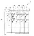
このEL表示装置1は、図1に示すように、複数の走査線101…と、各走査線101に対して直角に交差する方向に延びる複数の信号線102…と、各信号線102に並列に延びる複数の電源線103…とがそれぞれ配線された構成を有するとともに、走査線101…と信号線102…の各交点付近に、画素領域X…が設けられている。
信号線102には、シフトレジスタ、レベルシフタ、ビデオライン及びアナログスイッチを備えるデータ線駆動回路100が接続されている。また、走査線101には、シフトレジスタ及びレベルシフタを備える走査線駆動回路80が接続されている。
【0021】
さらに、画素領域X各々には、走査線101を介して走査信号がゲート電極に供給されるスイッチング用TFT112と、このスイッチング用TFT112を介して信号線102から共有される画素信号を保持する保持容量113と、該保持容量113によって保持された画素信号がゲート電極に供給される駆動用TFT123と、この駆動用TFT123を介して電源線103に電気的に接続したときに該電源線103から駆動電流が流れ込む画素電極(電極)23と、この画素電極23と陰極(電極)50との間に挟み込まれた機能層110とが設けられている。画素電極23と陰極50と機能層110により、発光素子(有機EL素子)が構成されている。
【0022】
このEL表示装置1によれば、走査線101が駆動されてスイッチング用TFT112がオン状態になると、そのときの信号線102の電位が保持容量113に保持され、該保持容量113の状態に応じて、駆動用TFT123のオン・オフ状態が決まる。そして、駆動用TFT123のチャネルを介して、電源線103から画素電極23に電流が流れ、さらに機能層110を介して陰極50に電流が流れる。機能層110は、これを流れる電流量に応じて発光する。
【0023】
次に、本実施形態のEL表示装置1の具体的な構成を図2〜図5を参照して説明する。
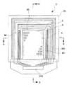
本実施形態のEL表示装置1は、図2に示すように電気絶縁性を備えた基板20と、スイッチング用TFT(図示せず)に接続された画素電極が基板20上にマトリックス状に配置されてなる画素電極域(図示せず)と、画素電極域の周囲に配置されるとともに各画素電極に接続される電源線(図示せず)と、少なくとも画素電極域上に位置する平面視ほぼ矩形の画素部3(図2中一点鎖線枠内)とを具備して構成されたアクティブマトリクス型のものである。なお、本発明においては、基板20と後述するようにこれの上に形成されるスイッチング用TFTや各種回路、及び層間絶縁膜などを含めて、基体と称している。(図3、4中では符号200で示している。)
【0024】
画素部3は、中央部分の実表示領域4(図2中二点鎖線枠内)と、実表示領域4の周囲に配置されたダミー領域5(一点鎖線および二点鎖線の間の領域)とに区画されている。
実表示領域4には、それぞれ画素電極を有する表示領域R、G、BがA−B方向およびC−D方向にそれぞれ離間してマトリックス状に配置されている。
また、実表示領域4の図2中両側には、走査線駆動回路80、80が配置されている。これら走査線駆動回路80、80は、ダミー領域5の下側に配置されたものである。
【0025】
さらに、実表示領域4の図2中上側には、検査回路90が配置されている。この検査回路90は、EL表示装置1の作動状況を検査するための回路であって、例えば検査結果を外部に出力する検査情報出力手段(図示せず)を備え、製造途中や出荷時の表示装置の品質、欠陥の検査を行うことができるように構成されたものである。なお、この検査回路90も、ダミー領域5の下側に配置されたものである。
【0026】
走査線駆動回路80および検査回路90は、その駆動電圧が、所定の電源部から駆動電圧導通部310(図3参照)および駆動電圧導通部340(図4参照)を介して、印加されるよう構成されている。また、これら走査線駆動回路80および検査回路90への駆動制御信号および駆動電圧は、このEL表示装置1の作動制御を行う所定のメインドライバなどから駆動制御信号導通部320(図3参照)および駆動電圧導通部350(図4参照)を介して、送信および印加されるようになっている。なお、この場合の駆動制御信号とは、走査線駆動回路80および検査回路90が信号を出力する際の制御に関連するメインドライバなどからの指令信号である。
【0027】
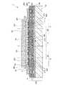
また、このEL表示装置1は、図3、図4に示すように基体200上に第1の電極(画素電極23)と本発明における機能層としての発光層60と第2の電極(陰極50)とを備えた発光素子(有機EL素子)を多数形成し、さらにこれらを覆ってガスバリア層30を形成したものである。
なお、本例では機能層を発光層60とし、この機能層を含む素子層を含んだ領域を素子領域(図示せず)としているが、本発明における機能層とは、代表的には発光層(エレクトロルミネッセンス層)であるものの、正孔注入層、正孔輸送層、電子注入層、電子輸送層などのキャリア注入層またはキャリア輸送層としてもよい。さらには、正孔阻止層(ホールブロッキング層)、電子阻止層(エレクトロン阻止層)であってもよい。
【0028】
基体200を構成する基板20としては、いわゆるトップエミッション型のEL表示装置の場合、この基板20の対向側であるガスバリア層30側から発光光を取り出す構成であるので、透明基板及び不透明基板のいずれも用いることができる。不透明基板としては、例えばアルミナ等のセラミックス、ステンレススチール等の金属シートに表面酸化などの絶縁処理を施したもの、また熱硬化性樹脂や熱可塑性樹脂、さらにはそのフィルム(プラスチックフィルム)などが挙げられる。
【0029】
また、いわゆるバックエミッション型のEL表示装置の場合には、基板20側から発光光を取り出す構成であるので、基板20としては、透明あるいは半透明のものが採用される。例えば、ガラス、石英、樹脂(プラスチック、プラスチックフィルム)等が挙げられ、特にガラス基板が好適に用いられる。なお、本実施形態では、ガスバリア層30側から発光光を取り出すトップエミッション型とし、よって基板20としては前記した不透明のもの、例えば不透明のプラスチックフィルムなどが用いられる。
【0030】
また、基板20上には、画素電極23を駆動するための駆動用TFT123などを含む回路部11が形成されており、その上に発光素子(有機EL素子)が多数設けられている。発光素子は、図5に示すように、陽極として機能する画素電極(第1の電極)23と、この画素電極23からの正孔を注入/輸送する正孔輸送層70と、電気光学物質の一つである有機EL物質を備える発光層60と、陰極(第2の電極)50とが順に形成されたことによって構成されたものである。このような構成のもとに、発光素子はその発光層60において、正孔輸送層70から注入された正孔と陰極50からの電子とが結合することにより、発光光を生じるようになっている。
【0031】
画素電極23は、本実施形態ではトップエミッション型であることから透明である必要がなく、したがって適宜な導電材料によって形成されている。
正孔輸送層70の形成材料としては、例えばポリチオフェン誘導体、ポリピロール誘導体など、またはそれらのドーピング体などが用いられる。具体的には、3,4−ポリエチレンジオシチオフェン/ポリスチレンスルフォン酸(PEDOT/PSS)[商品名;バイトロン−p(Bytron-p):バイエル社製]の分散液、すなわち、分散媒としてのポリスチレンスルフォン酸に3,4−ポリエチレンジオシチオフェンを分散させ、さらにこれを水に分散させた分散液などが用いられる。
【0032】
発光層60を形成するための材料としては、蛍光あるいは燐光を発光することが可能な公知の発光材料を用いることができる。具体的には、(ポリ)フルオレン誘導体(PF)、(ポリ)パラフェニレンビニレン誘導体(PPV)、ポリフェニレン誘導体(PP)、ポリパラフェニレン誘導体(PPP)、ポリビニルカルバゾール(PVK)、ポリチオフェン誘導体、ポリメチルフェニルシラン(PMPS)などのポリシラン系などが好適に用いられる。
また、これらの高分子材料に、ペリレン系色素、クマリン系色素、ローダミン系色素などの高分子系材料や、ルブレン、ペリレン、9,10−ジフェニルアントラセン、テトラフェニルブタジエン、ナイルレッド、クマリン6、キナクリドン等の低分子材料をドープして用いることもできる。
なお、前記の高分子材料に代えて、従来公知の低分子材料を用いることもできる。
また、必要に応じて、このような発光層60の上に電子注入層を形成してもよい。
【0033】
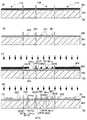
また、本実施形態において正孔輸送層70と発光層60とは、図3〜図5に示すように基体200上にて格子状に形成された親液性制御層25と有機バンク層221とによって囲まれて配置され、これにより囲まれた正孔輸送層70および発光層60は単一の発光素子(有機EL素子)を構成する素子層となっている。なお、格子状に形成された親液性制御層25および有機バンク層221にあって、特に最外周を形成する部分、すなわち発光層60の最外周位置のものの外側部を覆った状態でこれを囲む部分が、本発明における囲み部材201となっている。
ここで、囲み部材201については、特にその上部を形成する有機バンク層221における、外側部を形成する面201aの基体200表面に対する角度θが、110度以上となっている。このような角度としたのは、後述するようにこの上に形成する陰極50、さらにはガスバリア層30のステップカバレージ性を良好にし、外側部上での陰極やガスバリア層30の連続性を確保するためである。
【0034】
陰極50は、図3〜図5に示すように、実表示領域4およびダミー領域5の総面積より広い面積を備え、それぞれを覆うように形成されたもので、前記発光層60と有機バンク層221及び囲み部材201の上面、さらには囲み部材201の外側部を形成する面201aを覆った状態で基体200上に形成されたものである。なお、この陰極50は、図4に示すように前記囲み部材201の面201aの外側で基体200の外周部に形成された陰極用配線202に接続されている。この陰極用配線202にはフレキシブル基板203が接続されており、これによって陰極50は、陰極用配線202を介してフレキシブル基板203上の図示しない駆動IC(駆動回路)に接続されたものとなっている。
【0035】
陰極50を形成するための材料としては、本実施形態はトップエミッション型であることから光透過性である必要があり、したがって透明導電材料が用いられる。透明導電材料としてはITOが好適とされるが、これ以外にも、例えば酸化インジウム・酸化亜鉛系アモルファス透明導電膜(Indium Zinc Oxide :IZO/アイ・ゼット・オー)(登録商標))(出光興産社製)等を用いることができる。なお、本実施形態ではITOを用いるものとする。
【0036】
このような陰極50の上には、この陰極50の基体200上で露出する部位を覆った状態でガスバリア層30が設けられている。このガスバリア層30は、その内側に酸素や水分が浸入するのを防止するためのもので、これにより陰極50や発光層60への酸素や水分の浸入を防止し、酸素や水分による陰極50や発光層60の劣化等を抑えるようにしたものである。
【0037】
このガスバリア層30は、例えば無機化合物からなるもので、珪素化合物、すなわち珪素窒化物や珪素酸窒化物、珪素酸化物などによって形成されている。このようにガスバリア層30が珪素化合物で形成されていれば、特に陰極50がITOからなっていることにより、ガスバリア層30とこの陰極50との密着性がよくなり、したがってガスバリア層30が欠陥のない緻密な層となって酸素や水分に対するバリア性がより良好になる。
【0038】
また、このガスバリア層30としては、例えば前記の珪素化合物のうちの異なる層を積層した構造としてもよく、具体的には、陰極50側から珪素窒化物、珪素酸窒化物の順に形成し、あるいは陰極50側から珪素酸窒化物、珪素酸化物の順に形成してガスバリア層30を構成するのが好ましい。また、このような組み合わせ以外にも、組成比の異なる珪素酸窒化物を2層以上積層した場合に、陰極50側の層の酸素濃度がこれより外側の層の酸素濃度より低くなるように構成するのが好ましい。
このようにすれば、陰極50側がその反対側より酸素濃度が低くなることから、ガスバリア層30中の酸素が陰極50を通ってその内側の発光層60に到り、発光層60を劣化させてしまうといったことを防止することができ、これにより発光層60の長寿命化を図ることができる。
【0039】
また、ガスバリア層30としては、積層構造とすることなく、その組成を不均一にして特にその酸素濃度が連続的に、あるいは非連続的に変化するような構成としてもよく、その場合にも、陰極50側の酸素濃度が外側の酸素濃度より低くなるように構成するのが、前述した理由により好ましい。
また、このようなガスバリア層30の厚さとしては、10nm以上、500nm以下であるのが好ましい。10nm未満であると、膜の欠陥や膜厚のバラツキなどによって部分的に貫通孔が形成されてしまい、ガスバリア性が損なわれてしまうおそれがあるからであり、500nmを越えると、応力による割れが生じてしまうおそれがあるからである。
また、本実施形態ではトップエミッション型としていることから、ガスバリア層30は透光性を有する必要があり、したがってその材質や膜厚を適宜に調整することにより、本実施形態では可視光領域における光線透過率を例えば80%以上にしている。
【0040】
前記の発光素子の下方には、図5に示したように回路部11が設けられている。この回路部11は、基板20上に形成されて基体200を構成するものである。すなわち、基板20の表面にはSiO2 を主体とする下地保護層281が下地として形成され、その上にはシリコン層241が形成されている。このシリコン層241の表面には、SiO2 および/またはSiNを主体とするゲート絶縁層282が形成されている。
【0041】
また、前記シリコン層241のうち、ゲート絶縁層282を挟んでゲート電極242と重なる領域がチャネル領域241aとされている。なお、このゲート電極242は、図示しない走査線101の一部である。一方、シリコン層241を覆い、ゲート電極242を形成したゲート絶縁層282の表面には、SiO2 を主体とする第1層間絶縁層283が形成されている。
【0042】
また、シリコン層241のうち、チャネル領域241aのソース側には、低濃度ソース領域241bおよび高濃度ソース領域241Sが設けられる一方、チャネル領域241aのドレイン側には低濃度ドレイン領域241cおよび高濃度ドレイン領域241Dが設けられて、いわゆるLDD(Light Doped Drain )構造となっている。これらのうち、高濃度ソース領域241Sは、ゲート絶縁層282と第1層間絶縁層283とにわたって開孔するコンタクトホール243aを介して、ソース電極243に接続されている。このソース電極243は、前述した電源線103(図1参照、図5においてはソース電極243の位置に紙面垂直方向に延在する)の一部として構成されている。一方、高濃度ドレイン領域241Dは、ゲート絶縁層282と第1層間絶縁層283とにわたって開孔するコンタクトホール244aを介して、ソース電極243と同一層からなるドレイン電極244に接続されている。
【0043】
ソース電極243およびドレイン電極244が形成された第1層間絶縁層283の上層は、例えばアクリル系の樹脂成分を主体とする第2層間絶縁層284によって覆われている。この第2層間絶縁層284は、アクリル系の絶縁膜以外の材料、例えば、SiN、SiO2 などを用いることもできる。そして、ITOからなる画素電極23が、この第2層間絶縁層284の表面上に形成されるとともに、該第2層間絶縁層284に設けられたコンタクトホール23aを介してドレイン電極244に接続されている。すなわち、画素電極23は、ドレイン電極244を介して、シリコン層241の高濃度ドレイン領域241Dに接続されている。
【0044】
なお、走査線駆動回路80および検査回路90に含まれるTFT(駆動回路用TFT)、すなわち、例えばこれらの駆動回路のうち、シフトレジスタに含まれるインバータを構成するNチャネル型又はPチャネル型のTFTは、画素電極23と接続されていない点を除いて前記駆動用TFT123と同様の構造とされている。
【0045】
画素電極23が形成された第2層間絶縁層284の表面には、画素電極23と、前記した親液性制御層25及び有機バンク層221とが設けられている。親液性制御層25は、例えばSiO2 などの親液性材料を主体とするものであり、有機バンク層221は、アクリルやポリイミドなどからなるものである。そして、画素電極23の上には、親液性制御層25に設けられた開口部25a、および有機バンク221に囲まれてなる開口部221aの内部に、正孔輸送層70と発光層60とがこの順に積層されている。なお、本実施形態における親液性制御層25の「親液性」とは、少なくとも有機バンク層221を構成するアクリル、ポリイミドなどの材料と比べて親液性が高いことを意味するものとする。
以上に説明した基板20上の第2層間絶縁層284までの層が、回路部11を構成するものとなっている。
【0046】
ここで、本実施形態のEL表示装置1は、カラー表示を行うべく、各発光層60が、その発光波長帯域が光の三原色にそれぞれ対応して形成されている。例えば、発光層60として、発光波長帯域が赤色に対応した赤色用発光層60R、緑色に対応した緑色用発光層60G、青色に対応した青色用有機EL層60Bとをそれぞれに対応する表示領域R、G、Bに設け、これら表示領域R、G、Bをもってカラー表示を行う1画素が構成されている。また、各色表示領域の境界には、金属クロムをスパッタリングなどにて成膜した図示略のBM(ブラックマトリクス)が、例えば有機バンク層221と親液性化制御層25との間に形成されている。
【0047】
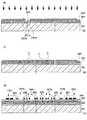
次に、本実施形態に係るEL表示装置1の製造方法の一例を、図6〜図10を参照して説明する。なお、本実施形態においては、電気光学装置としてのEL表示装置1が、トップエミッション型である場合について説明する。また、図6〜図10に示す各断面図は、図2中のA−B線の断面図に対応した図である。
【0048】
まず、図6(a)に示すように、基板20の表面に、下地保護層281を形成する。次に、下地保護層281上に、ICVD法、プラズマCVD法などを用いてアモルファスシリコン層501を形成した後、レーザアニール法又は急速加熱法により結晶粒を成長させてポリシリコン層とする。
【0049】
次いで、図6(b)に示すように、ポリシリコン層をフォトリソグラフィ法によりパターニングし、島状のシリコン層241、251および261を形成する。これらのうちシリコン層241は、表示領域内に形成され、画素電極23に接続される駆動用TFT123を構成するものであり、シリコン層251、261は、走査線駆動回路80に含まれるPチャネル型およびNチャネル型のTFT(駆動回路用TFT)をそれぞれ構成するものである。
【0050】
次に、プラズマCVD法、熱酸化法などにより、シリコン層241、251および261、下地保護層281の全面に厚さが約30nm〜200nmのシリコン酸化膜によって、ゲート絶縁層282を形成する。ここで、熱酸化法を利用してゲート絶縁層282を形成する際には、シリコン層241、251および261の結晶化も行い、これらのシリコン層をポリシリコン層とすることができる。
【0051】
また、シリコン層241、251および261にチャネルドープを行う場合には、例えば、このタイミングで約1×10¹²/cm2 のドーズ量でボロンイオンを打ち込む。その結果、シリコン層241、251および261は、不純物濃度(活性化アニール後の不純物にて算出)が約1×10¹⁷/cm3 の低濃度P型のシリコン層となる。
【0052】
次に、Pチャネル型TFT、Nチャネル型TFTのチャネル層の一部にイオン注入選択マスクを形成し、この状態でリンイオンを約1×10¹⁵/cm2 のドーズ量でイオン注入する。その結果、パターニング用マスクに対してセルフアライン的に高濃度不純物が導入されて、図6(c)に示すように、シリコン層241及び261中に高濃度ソース領域241Sおよび261S並びに高濃度ドレイン領域241Dおよび261Dが形成される。
【0053】
次に、図6(c)に示すように、ゲート絶縁層282の表面全体に、ドープドシリコンやシリサイド膜、あるいはアルミニウム膜やクロム膜、タンタル膜という金属膜からなるゲート電極形成用導電層502を形成する。この導電層502の厚さは概ね500nm程度である。その後、パターニング法により、図6(d)に示すように、Pチャネル型の駆動回路用TFTを形成するゲート電極252、画素用TFTを形成するゲート電極242、Nチャネル型の駆動回路用TFTを形成するゲート電極262を形成する。また、駆動制御信号導通部320(350)、陰極電源配線の第1層121も同時に形成する。なお、この場合、駆動制御信号導通部320(350)はダミー領域5に配設するものとされている。
【0054】
続いて、図6(d)に示すように、ゲート電極242,252および262をマスクとして用い、シリコン層241,251および261に対してリンイオンを約4×10¹³/cm2 のドーズ量でイオン注入する。その結果、ゲート電極242,252および262に対してセルフアライン的に低濃度不純物が導入され、図6(d)に示すように、シリコン層241および261中に低濃度ソース領域241bおよび261b、並びに低濃度ドレイン領域241cおよび261cが形成される。また、シリコン層251中に低濃度不純物領域251Sおよび251Dが形成される。
【0055】
次に、図7(e)に示すように、Pチャネル型の駆動回路用TFT252以外の部分を覆うイオン注入選択マスク503を形成する。このイオン注入選択マスク503を用いて、シリコン層251に対してボロンイオンを約1.5×10¹⁵/cm2 のドーズ量でイオン注入する。結果として、Pチャネル型駆動回路用TFTを構成するゲート電極252もマスクとして機能するため、シリコン層252中にセルフアライン的に高濃度不純物がドープされる。したがって、低濃度不純物領域251Sおよび251Dはカウンタードープされ、P型チャネル型の駆動回路用TFTのソース領域およびドレイン領域となる。
【0056】
次いで、図7(f)に示すように、基板20の全面にわたって第1層間絶縁層283を形成するとともに、フォトリソグラフィ法を用いて該第1層間絶縁層283をパターニングすることにより、各TFTのソース電極およびドレイン電極に対応する位置にコンタクトホールCを形成する。
【0057】
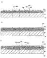
次に、図7(g)に示すように、第1層間絶縁層283を覆うように、アルミニウム、クロム、タンタルなどの金属からなる導電層504を形成する。この導電層504の厚さは概ね200nmないし800nm程度である。この後、導電層504のうち、各TFTのソース電極およびドレイン電極が形成されるべき領域240a、駆動電圧導通部310(340)が形成されるべき領域310a、陰極電源配線の第2層が形成されるべき領域122aを覆うようにパターニング用マスク505を形成するとともに、該導電層504をパターニングして、図8(h)に示すソース電極243、253、263、ドレイン電極244、254、264を形成する。
【0058】
次いで、図8(i)に示すように、これらが形成された第1層間絶縁層283を覆う第2層間絶縁層284を、例えばアクリル系樹脂などの高分子材料によって形成する。この第2層間絶縁層284は、約1〜2μm程度の厚さに形成されることが望ましい。なお、SiN、SiO2 により第2層間絶縁膜を形成することも可能であり、SiNの膜厚としては200nm、SiO2 の膜厚としては800nmに形成することが望ましい。
【0059】
次いで、図8(j)に示すように、第2層間絶縁層284のうち、駆動用TFTのドレイン電極244に対応する部分をエッチングにより除去してコンタクトホール23aを形成する。
その後、基板20の全面を覆うように画素電極23となる導電膜を形成する。そして、この透明導電膜をパターニングすることにより、図9(k)に示すように、第2層間絶縁層284のコンタクトホール23aを介してドレイン電極244と導通する画素電極23を形成すると同時に、ダミー領域のダミーパターン26も形成する、なお、図3、4では、これら画素電極23、ダミーパターン26を総称して画素電極23としている。
【0060】
ダミーパターン26は、第2層間絶縁層284を介して下層のメタル配線へ接続しない構成とされている。すなわち、ダミーパターン26は、島状に配置され、実表示領域に形成されている画素電極23の形状とほぼ同一の形状を有している。もちろん、表示領域に形成されている画素電極23の形状と異なる構造であってもよい。なお、この場合、ダミーパターン26は少なくとも前記駆動電圧導通部310(340)の上方に位置するものも含むものとする。
【0061】
次いで、図9(l)に示すように、画素電極23、ダミーパターン26上、および第2層間絶縁膜上に絶縁層である親液性制御層25を形成する。なお、画素電極23においては一部が開口する態様にて親液性制御層25を形成し、開口部25a(図3も参照)において画素電極23からの正孔移動が可能とされている。逆に、開口部25aを設けないダミーパターン26においては、絶縁層(親液性制御層)25が正孔移動遮蔽層となって正孔移動が生じないものとされている。続いて、親液性制御層25において、異なる2つの画素電極23の間に位置して形成された凹状部にBM(図示せず)を形成する。具体的には、親液性制御層25の前記凹状部に対して、金属クロムを用いスパッタリング法にて成膜する。
【0062】
次いで、図9(m)に示すように、親液性制御層25の所定位置、詳しくは前記BMを覆うように有機バンク層221を形成する。具体的な有機バンク層の形成方法としては、例えばアクリル樹脂、ポリイミド樹脂などのレジストを溶媒に溶解したものを、スピンコート法、ディップコート法などの各種塗布法により塗布して有機質層を形成する。なお、有機質層の構成材料は、後述するインクの溶媒に溶解せず、しかもエッチングなどによってパターニングし易いものであればどのようなものでもよい。
【0063】
続いて、有機質層をフォトリソグラフィ技術、エッチング技術を用いてパターニングし、有機質層にバンク開口部221aを形成することにより、開口部221aに壁面を有した有機バンク層221を形成する。ここで、この有機バンク層221にあたっては、特にその最外周を形成する部分、すなわち前述した本発明における囲み部材201の外側部を形成する面201aについて、その基体200表面に対する角度θを110度以上となるように形成するのが好ましい。このような角度に形成することにより、この上に形成する陰極50、さらにはガスバリア層30のステップカバレージ性を良好にすることができる。
なお、この場合、有機バンク層221は、少なくとも前記駆動制御信号導通部320の上方に位置するものを含むものとする。
【0064】
次いで、有機バンク層221の表面に、親液性を示す領域と、撥液性を示す領域とを形成する。本実施形態においては、プラズマ処理によって各領域を形成するものする。具体的には、該プラズマ処理を、予備加熱工程と、有機バンク層221の上面および開口部221aの壁面ならびに画素電極23の電極面23c、親液性制御層25の上面をそれぞれ親液性にする親インク化工程と、有機バンク層の上面および開口部の壁面を撥液性にする撥インク化工程と、冷却工程とで構成する。
【0065】
すなわち、基材(バンクなどを含む基板20)を所定温度、例えば70〜80℃程度に加熱し、次いで親インク化工程として大気雰囲気中で酸素を反応ガスとするプラズマ処理(O2 プラズマ処理)を行う。次いで、撥インク化工程として大気雰囲気中で4フッ化メタンを反応ガスとするプラズマ処理(CF4 プラズマ処理)を行い、その後、プラズマ処理のために加熱された基材を室温まで冷却することで、親液性および撥液性が所定箇所に付与されることとなる。
【0066】
なお、このCF4 プラズマ処理においては、画素電極23の電極面23cおよび親液性制御層25についても多少の影響を受けるが、画素電極23の材料であるITOおよび親液性制御層25の構成材料であるSiO2 、TiO2 などはフッ素に対する親和性に乏しいため、親インク化工程で付与された水酸基がフッ素基で置換されることがなく、親液性が保たれる。
【0067】
次いで、正孔輸送層形成工程によって正孔輸送層70の形成を行う。この正孔輸送層形成工程では、例えばインクジェット法等の液滴吐出法や、スピンコート法などにより、正孔輸送層材料を電極面23c上に塗布し、その後、乾燥処理および熱処理を行い、電極23上に正孔輸送層70を形成する。正孔輸送層材料を例えばインクジェット法で選択的に塗布する場合には、まず、インクジェットヘッド(図示略)に正孔輸送層材料を充填し、インクジェットヘッドの吐出ノズルを親液性制御層25に形成された前記開口部25a内に位置する電極面23cに対向させ、インクジェットヘッドと基材(基板20)とを相対移動させながら、吐出ノズルから1滴当たりの液量が制御された液滴を電極面23cに吐出する。次に、吐出後の液滴を乾燥処理し、正孔輸送層材料に含まれる分散媒や溶媒を蒸発させることにより、正孔輸送層70を形成する。
【0068】
ここで、吐出ノズルから吐出された液滴は、親液性処理がなされた電極面23c上にて広がり、親液性制御層25の開口部25a内に満たされる。その一方で、撥インク処理された有機バンク層221の上面では、液滴がはじかれて付着しない。したがって、液滴が所定の吐出位置からはずれて有機バンク層221の上面に吐出されたとしても、該上面が液滴で濡れることがなく、弾かれた液滴が親液性制御層25の開口部25a内に転がり込む。
なお、この正孔輸送層形成工程以降は、正孔輸送層70および発光層60の酸化を防止すべく、窒素雰囲気、アルゴン雰囲気などの不活性ガス雰囲気で行うのが好ましい。
【0069】
次いで、発光層形成工程によって発光層60の形成を行う。この発光層形成工程では、例えば前記のインクジェット法により、発光層形成材料を正孔輸送層70上に吐出し、その後、乾燥処理および熱処理を行うことにより、有機バンク層221に形成された開口部221a内に発光層60を形成する。この発光層形成工程では、正孔輸送層70の再溶解を防止するため、発光層形成材料に用いる溶媒として、正孔輸送層70に対して不溶な無極性溶媒を用いる。
なお、この発光層形成工程では、前記のインクジェット法によって例えば青色(B)の発光層形成材料を青色の表示領域に選択的に塗布し、乾燥処理した後、同様にして緑色(G)、赤色(R)についてもそれぞれその表示領域に選択的に塗布し、乾燥処理する。
また、必要に応じて、前述したようにこのような発光層60の上に電子注入層を形成してもよい。
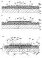
【0070】
次いで、図10(n)に示すように、陰極層形成工程によって陰極50の形成を行う。この陰極層形成工程では、例えば蒸着法等の物理的気相蒸着法によりITOを成膜し、陰極50とする。このとき、この陰極50については、前記発光層60と有機バンク層221及び囲み部材201の上面を覆うのはもちろん、囲み部材201の外側部を形成する面201aについてもこれを覆った状態となるように形成する。
【0071】
その後、図10(n)に示すように陰極50を覆って、すなわち基体200上にて露出する陰極50の全ての部位を覆った状態にガスバリア層30を形成し、本発明のEL表示装置(電気光学装置)を得る。ここで、このガスバリア層30の形成方法としては、先にスパッタリング法やイオンプレーティング法等の物理的気相蒸着法で成膜を行い、次いで、プラズマCVD法等の化学的気相蒸着法で成膜を行うのが好ましい。スパッタリング法やイオンプレーティング法等の物理的気相蒸着法は、一般に異質な基板表面に対しても比較的密着性の良い膜が得られるものの、得られる膜に関しては粒塊状で欠陥が発生しやすく、また応力の大きい被膜になりやすいなどの欠点がある。一方、化学的気相蒸着法では、応力が少なくステップカバーレッジ性に優れた欠陥が少なく緻密で良好な膜質のものが得られるものの、一般に異質な基板表面に対する密着性や造膜性が得られにくいといった欠点がある。そこで、初期の成膜については物理的気相蒸着法を採用して例えば必要な膜厚の半分あるいはそれ以上を形成し、後期の成膜において化学的気相蒸着法を用いることにより、先に形成した膜の欠陥を補うようにすれば、全体としてガスバリア性(酸素や水分に対するバリア性)に優れたガスバリア層30を比較的短時間で形成することができる。
【0072】
ここで、このガスバリア層30の形成については、前述したように同一の材料によって単層で形成してもよく、また異なる材料で複数の層に積層して形成してもよく、さらには、単層で形成するものの、その組成を膜厚方向で連続的あるいは非連続的に変化させるようにして形成してもよい。
異なる材料で複数の層に積層して形成する場合、例えば、前述したように物理的気相蒸着法で形成する内側の層(陰極50側の層)を珪素窒化物あるいは珪素酸窒化物などとし、化学的気相蒸着法で形成する外側の層を珪素酸窒化物あるいは珪素酸化物などとするのが好ましい。
【0073】
また、物理的気相蒸着法で内側の層を形成する際、成膜装置内に供給する酸素量を最初は少なくし、以下、連続的あるいは非連続的に増やすことにより、形成するガスバリア層30中の酸素濃度を陰極50側(内側)で低くし、外側ではこれより高くなるように形成してもよい。
なお、ガスバリア層30の形成については単一の成膜法で行ってもよいのはもちろんであり、その場合にも、前述したように酸素濃度を陰極50側(内側)で低くなるように形成するのが好ましい。
【0074】
このようなEL表示装置1にあっては、発光層60の最外周位置のものの外側部を覆った状態で囲み部材201が形成され、この囲み部材201の外側部を覆った状態に陰極50が形成され、さらにこの陰極50の基体200上で露出する部位を覆った状態でガスバリア層30が形成されているので、特に発光層60の外側部側が囲み部材201、陰極50、ガスバリア層30によって三重に封止されることにより、酸素や水分の浸入が確実に防止される。したがって、酸素や水分による発光層60や陰極50の劣化等を抑えることができ、発光素子を長寿命化することができる。
【0075】
また、ガスバリア層30の基体200に接する部分を全て珪素化合物とすることにより、基体200を構成する基板20が樹脂などの水分透過性のものであっても、この基板20上に形成される層間絶縁膜などとともにガスバリア層30で発光素子部分の外側全てを封止することができ、したがって発光素子をより長寿命化することができる。
また、アクティブマトリクス型であることから陰極50やガスバリア層30を発光素子毎に形成する必要がなく、したがってこれら陰極50やガスバリア層30に関して微細なパターン形成が不要となる。よって、これらを単純な成膜法で形成することができることから、生産性の向上を図ることができる。
【0076】
なお、前記EL表示装置1ではトップエミッション型を例にして説明したが、本発明はこれに限定されることなく、バックエミッション型にも、また、両側に発光光を出射するタイプのものにも適用可能である。特にバックエミッション型とした場合、陰極50には透明電極を用いる必要はないが、その場合にも、この陰極50の少なくともガスバリア層30と接する面側を、無機酸化物によって形成するのが好ましい。
このようにすれば、陰極50のガスバリア層30と接する面側が無機酸化物からなっているので、無機化合物あるいは珪素化合物などからなるガスバリア層30との密着性がよくなり、したがってガスバリア層30が欠陥のない緻密な層となって酸素や水分に対するバリア性がより良好になる。
【0077】
また、バックエミッション型、あるいは両側に発光光を出射するタイプのものとした場合、基体200に形成するスイッチング用TFT112や駆動用TFT123については、発光素子の直下ではなく、親液性制御層25および有機バンク層221の直下に形成するようにし、開口率を高めるのが好ましい。
また、前記EL表示装置1では本発明における第1の電極を陽極として機能させ、第2の電極を陰極として機能させたが、これらを逆にして第1の電極を陰極、第2の電極を陽極としてそれぞれ機能させるよう構成してもよい。ただし、その場合には、発光層60と正孔輸送層70との形成位置を入れ替えるようにする必要がある。
【0078】
また、前記実施形態では本発明の電気光学装置にEL表示装置1を適用した例を示したが、本発明はこれに限定されることなく、基本的に第2の電極が基体の外側に設けられるものであれば、どのような形態の電気光学装置にも適用可能である。
また、前記EL表示装置1では、ガスバリア層30を最外層としているが、従来一般的になされている封止基板や封止缶によってガスバリア層30の外側をさらに封止するようにしてもよい。
図11は、ガスバリア層30の外側を封止する例として、ガスバリア層30の上を覆って保護層204を設けた場合の実施形態を示している。この保護層204は、本実施形態ではガスバリア層30側に設けられた緩衝層205と、この上に設けられた表面保護層206とからなっている。
【0079】
緩衝層205は、前記ガスバリア層30に密着し、かつ外部からの機械的衝撃に対して緩衝機能を有するもので、例えばウレタン系、アクリル系、エポキシ系、ポリオレフィン系などの樹脂で、後述する表面保護層206より柔軟でガラス転移点の低い材料からなる接着剤によって形成されたものである。なお、このような接着剤には、シランカップリング剤またはアルコキシシランを添加しておくのが好ましく、このようにすれば、形成される緩衝層205とガスバリア層30との密着性がより良好になり、したがって機械的衝撃に対する緩衝機能が高くなる。また、特にガスバリア層30が珪素化合物で形成されている場合などでは、シランカップリング剤やアルコキシシランによってこのガスバリア層30との密着性を向上させることができ、したがってガスバリア層30のガスバリア性を高めることができる。
【0080】
表面保護層206は、緩衝層205上に設けられることにより、保護層204の表面側を構成するものであり、耐圧性や耐摩耗性、外部光反射防止性、ガスバリア性、紫外線遮断性などの機能の少なくとも一つを有してなる層である。具体的には、高分子層(プラスチックフィルム)やDLC(ダイアモンドライクカーボン)層、ガラスなどによって形成されるものである。
なお、この例のEL表示装置においては、トップエミッション型にする場合に前記表面保護層206、緩衝層205を共に透光性のものにする必要があるが、バックエミッション型とする場合にはその必要はない。
【0081】
このようにガスバリア層30上に保護層204を設ければ、表面保護層206が耐圧性や耐摩耗性、光反射防止性、ガスバリア性、紫外線遮断性などの機能を有していることにより、発光層60や陰極50、さらにはガスバリア層もこの表面保護層206によって保護することができ、したがって発光素子の長寿命化を図ることができる。
また、緩衝層205が機械的衝撃に対して緩衝機能を発揮するので、外部から機械的衝撃が加わった場合に、ガスバリア層30やこの内側の発光素子への機械的衝撃を緩和し、この機械的衝撃による発光素子の機能劣化を防止することができる。
【0082】
次に、本発明の電子機器を説明する。本発明の電子機器は、前記のEL表示装置(電気光学装置)を表示部として有したものであり、具体的には図12に示すものが挙げられる。
図12(a)は、携帯電話の一例を示した斜視図である。図12(a)において、符号1000は携帯電話本体を示し、符号1001は前記のEL表示装置を用いた表示部を示している。
図12(b)は、腕時計型電子機器の一例を示した斜視図である。図12(b)において、符号1100は時計本体を示し、符号1101は前記のEL表示装置を用いた表示部を示している。
図12(c)は、ワープロ、パソコンなどの携帯型情報処理装置の一例を示した斜視図である。図12(c)において、符号1200は情報処理装置、符号1201はキーボードなどの入力部、符号1202は前記のEL表示装置を用いた表示部、符号1203は情報処理装置本体を示している。
図12(a)〜(c)に示すそれぞれの電子機器は、前記EL表示装置(電気光学装置)を有した表示部を備えているので、表示部を構成するEL表示装置の発光素子の長寿命化が図られたものとなる。
【0083】
「実験例1」
本発明におけるガスバリア層のガスバリア性を確認するため、以下の実験を行った。
・試料作製
基板としてPET(ポリエチレンテレフタレート;東レ製「T60」厚さ188μm)を用い、この上に電極材料、ガスバリア層形成材料を以下のようにして成膜し、試料を作製した。
・無機酸化物電極(ITO)の作製(成膜条件)
成膜装置としてマグネトロンDCスパッタを用い、ターゲット原料としてInSnOを用いた。真空度を0.4Pa、導入ガスをAr、O2 として成膜を行い、厚さ100nmのITO膜を作製した。
・金属電極(Al)の作製(成膜条件)
成膜装置として抵抗加熱蒸着装置を用い、原料として高純度のAlを用いた。
真空度を1.0×10⁻⁵Paとして成膜を行い、厚さ25nmのAl膜を作製した。
・ガスバリア層としての珪素化合物(SiOx、SiNx、SiOxNy)の作製(成膜条件)
成膜装置としてECR(電子サイクロン共鳴)を用い、ターゲット原料としてSiを用いた。真空度を0.2Pa、導入ガスをAr、O2 、N2 として成膜を行い、厚さ10〜150nmの珪素化合物膜を作製した。なお、導入ガスについては使用がすやその流量を試料毎に適宜に調整した。
・測定
得られた試料に対し、「JIS−Z0208」に準拠して水蒸気透過率の測定を行った。測定結果(測定値)を以下に示す(水蒸気透過率の単位は[g/m2・24時間]である)。なお、測定条件は60℃、90%RHとした。また、基板のみの水蒸気透過率や基板に電極材料のみを成膜したものについても、参考としてその水蒸気透過率を測定し、結果を以下に示す。さらに、珪素化合物膜単独での水蒸気透過率を以下の式に基づいて計算(換算)し、得られた値を参考として前記測定結果に併記した。
珪素化合物膜単独の換算方法
(1/A)=(1/B)+(1/C)
ただし、A;(PETまたはPRT+ITO膜)+珪素化合物膜の測定値
B;(PETまたはPRT+ITO膜)の測定値
C;珪素化合物膜単独の計算(換算)値
【0084】
なお、珪素化合物膜の屈折率を、自動エリプソメータ「NARY−102」(ファイブラボ株式会社製)によって測定波長領域を632nmとして測定したところ、SiOxは1.43、SiNxは1.99、SiOxNyは1.65であった。(ただし、SiOxNyについてはその組成を変えることにより、屈折率も任意に変更可能である)
【0086】
「実験例2」
珪素化合物膜(SiOx)の膜厚を変え、その水蒸気透過率を「実施例1」と同様に測定し、珪素化合物膜(SiOx)の膜厚依存性を調べた。得られた結果を以下に示す。なお、珪素化合物膜(SiOx)を基板(PET)上に直接形成するのでなく、ITO膜を介して形成した先の例(SiOxの膜厚が70nm)も併記する。また、得られた結果をグラフとして図13にも示す。
【図面の簡単な説明】
【図1】 本発明のEL表示装置の配線構造を示す模式図である。
【図2】 本発明のEL表示装置の構成を模式的に示す平面図である。
【図3】 図2のA−B線に沿う断面図である。
【図4】 図2のC−D線に沿う断面図である。
【図5】 図3の要部拡大断面図である。
【図6】 EL表示装置の製造方法を工程順に説明する断面図である。
【図7】 図6に続く工程を説明するための断面図である。
【図8】 図7に続く工程を説明するための断面図である。
【図9】 図8に続く工程を説明するための断面図である。
【図10】 図9に続く工程を説明するための断面図である。
【図11】 本発明の他のEL表示装置の要部拡大断面図である。
【図12】 (a)〜(c)は本発明の電子機器を示す斜視図である。
【図13】 珪素化合物膜の膜厚依存性を示すグラフである。
【符号の説明】
1 EL表示装置(電気光学装置)、23 画素電極(第1の電極)、
30 ガスバリア層、50 陰極(第2の電極)、60 発光層(機能層)、
200 基体、201 囲み部材、204 保護層、205 緩衝層、
206 表面保護層[0001]
BACKGROUND OF THE INVENTION
The present invention relates to an electro-optical device, a method for manufacturing the electro-optical device, and an electronic apparatus including the electro-optical device.
[0002]
[Prior art]
Conventionally, in an electro-optical device such as an organic electroluminescence (hereinafter abbreviated as organic EL) display device, an anode, a hole injection layer, a light-emitting layer made of an electro-optical material such as an EL material, a cathode, and the like are provided on a substrate. A laminated structure is known. The organic EL element constituting such an organic EL display device has a lifetime as a light-emitting element due to deterioration of the electro-optical material forming the light-emitting layer due to oxygen, moisture, etc., or decrease in conductivity due to oxygen, moisture, etc. of the cathode. There was a problem of shortening.
As a technique for solving such a problem, conventionally, for example, a method of manufacturing an organic EL element in which a protective film is formed so as to cover a light emitting layer and a cathode is known (see, for example, Patent Document 1).
[0003]
[Patent Document 1]
JP-A-8-111286 (FIG. 1)
[0004]
[Problems to be solved by the invention]
However, in the method of manufacturing the organic EL element, there is no disclosure about a case where there are a large number of light-emitting layers, and therefore it is difficult to apply this technique to an electro-optical device including a display unit including a large number of organic EL elements. is there. Therefore, it is difficult to extend the life of the light emitting element (organic EL element) in the electro-optical device.
[0005]
The present invention has been made in view of the above circumstances, and an object of the present invention is to easily and reliably allow oxygen and moisture to enter the light emitting layer and the electrode even in an electro-optical device having a large number of light emitting layers. It is an object of the present invention to provide an electro-optical device and an electronic apparatus equipped with the electro-optical device that can prevent the light emission element and thereby extend the life of the light-emitting element.
[0006]
[Means for Solving the Problems]
In order to achieve the above object, an electro-optical device of the present invention is provided with a first electrode provided on a base, a functional layer provided above the first electrode, and a functional layer provided above the functional layer. An element region in which a plurality of elements including a second electrode are formed; and the side of the functional layer included in the element closest to the outer periphery of the base in the element region is covered on the base An enclosing member provided and a gas barrier layer covering the second electrode, and the outer peripheral side portion of the enclosing member is covered with the second electrode,The second electrode is in contact with the substrate; The gas barrier layerIs The portion in contact with the substrate, the portion of the gas barrier layer in contact with the substrate and the second electrode is made of a silicon compound, and at least the surface side of the second electrode in contact with the gas barrier layer is made of an inorganic oxide, SaidFunctional layer Is sealed by the surrounding member, the second electrode, and the gas barrier layer.
Further, in the electro-optical device, a portion of the gas barrier layer that is in contact with the base and the second electrode is made of silicon oxynitride.
In the electro-optical device, the gas barrier layer includes at least a layer made of silicon oxynitride provided on the second electrode side and a layer made of silicon oxide provided on the layer. It is characterized by that.
In the electro-optical device, the gas barrier layer is made of silicon oxynitride, and the oxygen concentration on the second electrode side is lower than the oxygen concentration on the outside.
Further, in the electro-optical device, the element exhibits a function when carriers supplied from the first electrode or the second electrode pass through the functional layer. To do.
Further, in the electro-optical device, an angle formed between a surface forming the outer portion of the surrounding member and the surface of the base is 110 degrees or more.
Further, the electro-optical device is characterized in that the electro-optical device is an active matrix type.
In the electro-optical device, a protective layer may be provided on the gas barrier layer so as to cover the gas barrier layer.
Further, in the electro-optical device, the protective layer has a surface protective layer on a surface side thereof.
In the electro-optical device, the protective layer includes a buffer layer on the gas barrier layer side, which is in close contact with the gas barrier layer and has a buffer function against mechanical shock. .
In the electro-optical device, the buffer layer contains a silane coupling agent or alkoxysilane.
According to another aspect of the invention, there is provided a method for manufacturing the electro-optical device, the step of forming an enclosing member in the element region on the substrate, the step of forming a plurality of first electrodes in the enclosing member in the element region on the substrate, Forming a functional layer above the first electrode; covering the second electrode above the functional layer; and covering an outer peripheral side of the surrounding member.And contact with the base And a step of forming a gas barrier layer that covers the second electrode and is in contact with the substrate. In the step of forming the gas barrier layer, an initial formation is performed using a physical vapor deposition method. A film is formed, and the latter film formation is performed using a chemical vapor deposition method.
In the method of manufacturing the electro-optical device, the second electrode side of the gas barrier layer is formed of silicon oxynitride.
The method of manufacturing the electro-optical device is characterized in that at least a surface side of the second electrode in contact with the gas barrier layer is formed of an inorganic oxide.
[0007]
According to this electro-optical device, the surrounding member surrounding member is provided so as to cover the outer peripheral side portion of the element layer included in the element region, and the outer peripheral side portion of the surrounding member is covered with the second electrode. In addition, since the second electrode is covered with the gas barrier layer, the side portion on the outer peripheral side of the element layer included in the element region is sealed in triplicate by the surrounding member, the second electrode, and the gas barrier layer. Thus, intrusion of oxygen and moisture is surely prevented, whereby deterioration of the element layer and electrodes due to oxygen and moisture is suppressed, and the life of the element can be extended.
In addition, since it is not necessary to form a second electrode or gas barrier layer for each element layer (for example, a light emitting element layer), it is not necessary to form a fine pattern, and thus can be formed by a simple film formation method. It is possible to improve the performance.
[0008]
In the electro-optical device, the element layer may exhibit a function when carriers supplied from the first electrode or the second electrode pass through the element layer.
When carriers pass through the element layer, at least a portion having different probability of existence of electrons and holes is generated, and the charge balance of the portion may be lost. Such a part is generally highly reactive and, for example, reacts with oxygen, water, or the like, resulting in a structural defect. The structural defect becomes a carrier trapping site and causes a decrease in the function of the element layer. For this reason, it is necessary to sufficiently protect the element layer from deterioration factors such as oxygen and water. However, the element layer can be protected from oxygen and water by the surrounding member and the gas barrier layer.
In addition, since the carrier injection efficiency is greatly affected by the state of the electrode, in order to maintain appropriate injection efficiency, it is necessary to sufficiently protect it from oxygen, water, etc., which are degradation factors of the electrode. As described above, the surrounding member, the gas barrier layer, and the like can protect the electrode from oxygen and water.
[0009]
In the electro-optical device, the gas barrier layer is preferably an inorganic compound or a silicon compound.
In this way, for example, when the second electrode is made of an inorganic oxide such as ITO (indium tin oxide), a metal, an alloy, or the like, the gas barrier layer is made of an inorganic compound or a silicon compound. Therefore, the gas barrier layer becomes a dense layer without defects, and the barrier property against oxygen and moisture becomes better.
[0010]
In the electro-optical device, it is preferable that at least a surface side of the second electrode in contact with the gas barrier layer is made of an inorganic oxide.
In this case, since the surface side of the second electrode that contacts the gas barrier layer is made of an inorganic oxide, the adhesion with the gas barrier layer made of an inorganic compound or silicon compound is improved, and therefore the gas barrier layer is free from defects. It becomes a dense layer and has better barrier properties against oxygen and moisture.
[0011]
In the electro-optical device, it is preferable that an angle formed between the surface forming the outer portion of the surrounding member and the surface of the base is 110 degrees or more.
If it does in this way, the coverage property of the 2nd electrode and gas barrier layer which covers the outer side part of a surrounding member will become favorable, and the continuity of the 2nd electrode and gas barrier layer on this outer side part will be ensured.
[0012]
The electro-optical device is preferably an active matrix type.
In this way, since it is not necessary to form the second electrode for each light emitting element, it is not necessary to form a fine pattern. Therefore, the second electrode can be formed by a simple film formation method. It is possible to improve the performance.
[0013]
In the electro-optical device, it is preferable that the gas barrier layer is configured such that the oxygen concentration on the second electrode side is lower than the oxygen concentration on the outside.
With this configuration, it is possible to prevent oxygen in the gas barrier layer from reaching the light emitting layer through the second electrode and deteriorating the light emitting layer, thereby extending the life of the light emitting layer. It is done.
[0014]
In the electro-optical device, it is preferable that a protective layer is provided on the gas barrier layer so as to cover the gas barrier layer.
In this way, the light emitting layer and the electrode are protected by the protective layer, so that deterioration of the light emitting layer and the electrode due to oxygen and moisture can be suppressed, and thus the life of the light emitting element can be extended.
[0015]
In this electro-optical device, the protective layer preferably has a surface protective layer on the surface side.
In this case, for example, the surface protective layer is provided with a layer having functions such as pressure resistance, abrasion resistance, light reflection preventing property, gas barrier property, and ultraviolet blocking property, so that a light emitting layer, an electrode, and further a gas barrier layer are provided. Is also protected by this surface protective layer, so that the lifetime of the light emitting element is extended.
[0016]
In this electro-optical device, it is preferable that the protective layer has, on the gas barrier layer side, a buffer layer that is in close contact with the gas barrier layer and has a buffer function against mechanical shock.
In this way, the buffer layer exhibits a buffering function against the mechanical shock, so that the mechanical shock to the gas barrier layer and the light emitting element inside the buffer layer is mitigated and the functional deterioration due to the mechanical shock is prevented. be able to.
[0017]
Such a buffer layer preferably contains a silane coupling agent or alkoxysilane.
In this way, the adhesion with the gas barrier layer becomes better, and therefore the buffering function against mechanical impact is enhanced.
[0018]
An electronic apparatus according to the present invention includes the electro-optical device described above.
According to this electronic apparatus, since the light-emitting element has an electro-optical device whose life is extended by suppressing deterioration of the light-emitting layer and electrodes due to oxygen and moisture, the product life of the electronic apparatus itself is also good. Become.
[0019]
DETAILED DESCRIPTION OF THE INVENTION
As an embodiment of the electro-optical device of the present invention, an EL display device using an electroluminescent material, particularly an organic electroluminescence (EL) material, which is an example of an electro-optical material will be described.
First, the wiring structure of the EL display device of this embodiment will be described with reference to FIG.
An EL display device (electro-optical device) 1 illustrated in FIG. 1 is an active matrix EL display device using a thin film transistor (hereinafter abbreviated as TFT) as a switching element.
[0020]
As shown in FIG. 1, the
A data
[0021]
Further, in each pixel region X, a switching
[0022]
According to the
[0023]
Next, a specific configuration of the
In the
[0024]
The
In the
Further, scanning
[0025]
Further, an
[0026]
The scanning
[0027]
In addition, as shown in FIGS. 3 and 4, the
In this example, the functional layer is the
[0028]
In the case of a so-called top emission type EL display device, the
[0029]
In the case of a so-called back emission type EL display device, since the emitted light is extracted from the
[0030]
A
[0031]
Since the
As a material for forming the
[0032]
As a material for forming the
In addition, these polymer materials include polymer materials such as perylene dyes, coumarin dyes, rhodamine dyes, rubrene, perylene, 9,10-diphenylanthracene, tetraphenylbutadiene, Nile red, coumarin 6, and quinacridone. It can also be used by doping a low molecular weight material such as.
In addition, it replaces with the said polymeric material, and a conventionally well-known low molecular material can also be used.
In addition, an electron injection layer may be formed on the
[0033]
In the present embodiment, the
Here, with respect to the surrounding
[0034]
As shown in FIGS. 3 to 5, the
[0035]
As a material for forming the
[0036]
On the
[0037]
The
[0038]
The
In this way, since the oxygen concentration on the
[0039]
Further, the
In addition, the thickness of the
In addition, since the top emission type is used in the present embodiment, the
[0040]
A
[0041]
In the
[0042]
Further, in the
[0043]
The upper layer of the first
[0044]
Note that TFTs (driving circuit TFTs) included in the scanning
[0045]
On the surface of the second
The layers up to the second
[0046]
Here, in the
[0047]
Next, an example of a method for manufacturing the
[0048]
First, as shown in FIG. 6A, a base
[0049]
Next, as shown in FIG. 6B, the polysilicon layer is patterned by a photolithography method to form island-like silicon layers 241, 251 and 261. Among these, the
[0050]
Next, a
[0051]
In addition, when channel doping is performed on the silicon layers 241, 251 and 261, for example, about 1 × 10 10 at this timing.12 / Cm2 Boron ions are implanted at a dose of. As a result, the silicon layers 241, 251 and 261 have an impurity concentration (calculated by the impurities after activation annealing) of about 1 × 10.17 / Cm3 This is a low concentration P-type silicon layer.
[0052]
Next, an ion implantation selection mask is formed in part of the channel layer of the P-channel TFT and the N-channel TFT, and in this state, phosphorus ions are about 1 × 10 × 10.15 / Cm2 Ion implantation is performed with a dose amount of. As a result, high concentration impurities are introduced into the patterning mask in a self-aligned manner, and as shown in FIG. 6C, the high
[0053]
Next, as shown in FIG. 6C, a gate electrode forming
[0054]
Subsequently, as shown in FIG. 6 (d), the
[0055]
Next, as shown in FIG. 7E, an ion
[0056]
Next, as shown in FIG. 7 (f), a first
[0057]
Next, as shown in FIG. 7G, a
[0058]
Next, as shown in FIG. 8I, a second
[0059]
Next, as shown in FIG. 8J, a portion of the second
Thereafter, a conductive film to be the
[0060]
The
[0061]
Next, as shown in FIG. 9L, a
[0062]
Next, as shown in FIG. 9 (m), an
[0063]
Subsequently, the organic layer is patterned using a photolithography technique and an etching technique, and a
In this case, the
[0064]
Next, a region showing lyophilicity and a region showing liquid repellency are formed on the surface of the
[0065]
That is, the base material (
[0066]
This CF4 In the plasma processing, the electrode surface 23c of the
[0067]
Next, the
[0068]
Here, the droplets ejected from the ejection nozzle spread on the electrode surface 23c that has been subjected to the lyophilic treatment, and are filled in the
In addition, after this hole transport layer formation process, in order to prevent the oxidation of the
[0069]
Next, the
In this light emitting layer forming step, for example, a blue (B) light emitting layer forming material is selectively applied to a blue display region by the above-described ink jet method, dried, and then similarly treated with green (G), red (R) is also selectively applied to the display area and dried.
If necessary, an electron injection layer may be formed on the
[0070]
Next, as shown in FIG. 10 (n), the
[0071]
Thereafter, as shown in FIG. 10 (n), the
[0072]
Here, the
In the case of stacking a plurality of layers with different materials, for example, as described above, the inner layer (layer on the
[0073]
When forming the inner layer by physical vapor deposition, the
The
[0074]
In such an
[0075]
Moreover, even if the portion of the
Further, since it is an active matrix type, it is not necessary to form the
[0076]
The
In this way, since the surface side of the
[0077]
Further, in the case of a back emission type or a type that emits emitted light on both sides, the switching
In the
[0078]
In the above embodiment, the
In the
FIG. 11 shows an embodiment in which a
[0079]
The
[0080]
The surface
In the EL display device of this example, both the surface
[0081]
If the
In addition, since the
[0082]
Next, the electronic apparatus of the present invention will be described. The electronic apparatus of the present invention has the above-described EL display device (electro-optical device) as a display unit, and specifically, the one shown in FIG.
FIG. 12A is a perspective view showing an example of a mobile phone. In FIG. 12A,
FIG. 12B is a perspective view showing an example of a wristwatch type electronic device. In FIG. 12B,
FIG. 12C is a perspective view illustrating an example of a portable information processing apparatus such as a word processor or a personal computer. In FIG. 12C,
Each of the electronic devices shown in FIGS. 12A to 12C includes a display unit having the EL display device (electro-optical device). Therefore, the length of the light emitting element of the EL display device that constitutes the display unit. Life expectancy will be improved.
[0083]
"
In order to confirm the gas barrier property of the gas barrier layer in the present invention, the following experiment was conducted.
・ Sample preparation
PET (polyethylene terephthalate; “T60” thickness 188 μm manufactured by Toray Industries, Inc.) was used as a substrate, and an electrode material and a gas barrier layer forming material were formed thereon as follows to prepare a sample.
・ Production of inorganic oxide electrode (ITO) (film formation conditions)
Magnetron DC sputtering was used as the film forming apparatus, and InSnO was used as the target material. The degree of vacuum is 0.4 Pa, the introduced gas is Ar, O2 As a film, an ITO film having a thickness of 100 nm was produced.
・ Production of metal electrodes (Al) (deposition conditions)
A resistance heating vapor deposition apparatus was used as a film forming apparatus, and high-purity Al was used as a raw material.
The degree of vacuum is 1.0 × 10⁻⁵ A film was formed as Pa, and an Al film having a thickness of 25 nm was produced.
-Production of silicon compounds (SiOx, SiNx, SiOxNy) as gas barrier layers (film formation conditions)
ECR (electron cyclone resonance) was used as the film forming apparatus, and Si was used as the target material. The degree of vacuum is 0.2 Pa, the introduced gas is Ar, O2 , N2 As a film, a silicon compound film having a thickness of 10 to 150 nm was produced. Note that the flow rate of the introduced gas was adjusted appropriately for each sample as soon as it was used.
・ Measurement
The water vapor transmission rate of the obtained sample was measured according to “JIS-Z0208”. The measurement results (measured values) are shown below (the unit of water vapor transmission rate is [g / m2 24 hours]). The measurement conditions were 60 ° C. and 90% RH. In addition, the water vapor transmission rate of only the substrate or the electrode material alone formed on the substrate was also measured for reference, and the results are shown below. Furthermore, the water vapor transmission rate of the silicon compound film alone was calculated (converted) based on the following formula, and the obtained value was also written in the measurement result as a reference.
Conversion method for silicon compound film alone
(1 / A) = (1 / B) + (1 / C)
However, A: (PET or PRT + ITO film) + Measured value of silicon compound film
B: Measured value of (PET or PRT + ITO film)
C: Calculation (conversion) value of silicon compound film alone
[0084]
The refractive index of the silicon compound film was measured with an automatic ellipsometer “NARY-102” (manufactured by Fibrabo Inc.) at a measurement wavelength region of 632 nm. .65. (However, the refractive index of SiOxNy can be arbitrarily changed by changing its composition.)
[0086]
"Experimental example 2"
The film thickness dependency of the silicon compound film (SiOx) was measured by changing the film thickness of the silicon compound film (SiOx) and measuring the water vapor transmission rate in the same manner as in Example 1. The obtained results are shown below. Note that the silicon compound film (SiOx) is not directly formed on the substrate (PET), but the previous example (SiOx film thickness is 70 nm) formed through the ITO film is also shown. Moreover, the obtained result is also shown in FIG. 13 as a graph.
[Brief description of the drawings]
FIG. 1 is a schematic diagram showing a wiring structure of an EL display device of the present invention.
FIG. 2 is a plan view schematically showing a configuration of an EL display device of the present invention.
3 is a cross-sectional view taken along the line AB of FIG.
4 is a cross-sectional view taken along line CD of FIG.
5 is an enlarged cross-sectional view of a main part of FIG.
6 is a cross-sectional view illustrating a method for manufacturing an EL display device in the order of steps. FIG.
7 is a cross-sectional view for illustrating a process following the process in FIG. 6. FIG.
FIG. 8 is a cross-sectional view for explaining a process following the process in FIG. 7;
FIG. 9 is a cross-sectional view for explaining a process following the process in FIG. 8;
10 is a cross-sectional view for explaining a process following the process in FIG. 9; FIG.
FIG. 11 is an enlarged cross-sectional view of a main part of another EL display device of the present invention.
12A to 12C are perspective views showing an electronic apparatus of the present invention.
FIG. 13 is a graph showing the film thickness dependence of a silicon compound film.
[Explanation of symbols]
1 EL display device (electro-optical device), 23 pixel electrode (first electrode),
30 gas barrier layer, 50 cathode (second electrode), 60 light emitting layer (functional layer),
200 substrate, 201 enclosing member, 204 protective layer, 205 buffer layer,
206 Surface protective layer
Claims (15)
Translated fromJapanese前記素子領域のうち、前記基体の外周に最も近接する素子に含まれる機能層の前記外周側の側部を覆い、前記基体上に設けられた囲み部材と、
前記第2の電極を覆うガスバリア層と、を含み、
前記囲み部材の前記外周側の側部は、前記第2の電極により覆われ、
前記第2の電極は前記基体に接しており、
前記ガスバリア層は前記基体と接しており、
前記ガスバリア層の、前記基体及び前記第2の電極と接する部分は、珪素化合物からなり、
前記第2の電極の少なくともガスバリア層と接する面側が、無機酸化物からなり、
前記機能層は、前記囲み部材、前記第2の電極、及び前記ガスバリア層により封止されている
ことを特徴とする電気光学装置。An element region in which a plurality of elements including a first electrode provided on a base, a functional layer provided above the first electrode, and a second electrode provided above the functional layer are formed. When,
Of the element region, the side of the outer peripheral side of the functional layer included in the element that is closest to the outer periphery of the base, and a surrounding member provided on the base;
A gas barrier layer covering the second electrode,
A side portion on the outer peripheral side of the surrounding member is covered with the second electrode,
The second electrode is in contact with the substrate;
The gas barrier layeris in contact with the substrate;
The portion of the gas barrier layer that is in contact with the base and the second electrode is made of a silicon compound,
The surface side in contact with at least the gas barrier layer of the second electrode is made of an inorganic oxide,
Thefunctional layer is sealed by the surrounding member, the second electrode, and the gas barrier layer.
基体上の素子領域の前記囲み部材内に第1の電極を複数形成する工程と、
前記第1の電極の上方に機能層を形成する工程と、
前記機能層の上方に第2の電極を、前記囲み部材の外周側の側部を覆い、かつ、前記基体に当接させて形成する工程と、
前記第2の電極を覆い、かつ前記基体と接するガスバリア層を形成する工程と、を備え、
前記ガスバリア層を形成する工程では、物理的気相蒸着法を用いて初期の成膜を行い、化学的気相蒸着法を用いて後期の成膜を行うことを特徴とする電気光学装置の製造方法。Forming an enclosing member in an element region on the substrate;
Forming a plurality of first electrodes in the surrounding member of the element region on the substrate;
Forming a functional layer above the first electrode;
A second electrode above the functional layer,not covering the outer periphery side of saidenclosure, and a step of formingis brought into contact with the substrate,
Forming a gas barrier layer that covers the second electrode and is in contact with the substrate,
In the step of forming the gas barrier layer, an initial film formation is performed using a physical vapor deposition method, and a later film formation is performed using a chemical vapor deposition method. Method.
Priority Applications (10)
| Application Number | Priority Date | Filing Date | Title |
|---|---|---|---|
| JP2002311109AJP3997888B2 (en) | 2002-10-25 | 2002-10-25 | Electro-optical device, method of manufacturing electro-optical device, and electronic apparatus |
| KR10-2003-0067264AKR100515110B1 (en) | 2002-10-25 | 2003-09-29 | Electro-optical device and electronic apparatus |
| CN2009101644255ACN101615629B (en) | 2002-10-25 | 2003-10-15 | Electro-optical device and electronic apparatus |
| CNB2003101013640ACN100527432C (en) | 2002-10-25 | 2003-10-15 | Electro-optical devices and electronic equipment |
| TW092129603ATWI231051B (en) | 2002-10-25 | 2003-10-24 | Electro-optical device and electronic apparatus |
| US10/691,671US7242375B2 (en) | 2002-10-25 | 2003-10-24 | Electro-optical device and electronic apparatus |
| US11/798,743US20070224907A1 (en) | 2002-10-25 | 2007-05-16 | Electro-optical device and electronic apparatus |
| US12/461,110US8779658B2 (en) | 2002-10-25 | 2009-07-31 | Electro-optical device and electronic apparatus |
| US14/294,811US9065074B2 (en) | 2002-10-25 | 2014-06-03 | Electro-optical device and electronic apparatus |
| US14/713,567US9450204B2 (en) | 2002-10-25 | 2015-05-15 | Electro-optical device and electronic apparatus |
Applications Claiming Priority (1)
| Application Number | Priority Date | Filing Date | Title |
|---|---|---|---|
| JP2002311109AJP3997888B2 (en) | 2002-10-25 | 2002-10-25 | Electro-optical device, method of manufacturing electro-optical device, and electronic apparatus |
Related Child Applications (3)
| Application Number | Title | Priority Date | Filing Date |
|---|---|---|---|
| JP2005161255ADivisionJP4466479B2 (en) | 2005-06-01 | 2005-06-01 | Electro-optical device and electronic apparatus |
| JP2005161257ADivisionJP4613700B2 (en) | 2005-06-01 | 2005-06-01 | Electro-optical device and electronic apparatus |
| JP2005161256ADivisionJP4736544B2 (en) | 2005-06-01 | 2005-06-01 | Electro-optical device and electronic apparatus |
Publications (2)
| Publication Number | Publication Date |
|---|---|
| JP2004146244A JP2004146244A (en) | 2004-05-20 |
| JP3997888B2true JP3997888B2 (en) | 2007-10-24 |
Family
ID=32456435
Family Applications (1)
| Application Number | Title | Priority Date | Filing Date |
|---|---|---|---|
| JP2002311109AExpired - LifetimeJP3997888B2 (en) | 2002-10-25 | 2002-10-25 | Electro-optical device, method of manufacturing electro-optical device, and electronic apparatus |
Country Status (5)
| Country | Link |
|---|---|
| US (5) | US7242375B2 (en) |
| JP (1) | JP3997888B2 (en) |
| KR (1) | KR100515110B1 (en) |
| CN (2) | CN101615629B (en) |
| TW (1) | TWI231051B (en) |
Families Citing this family (49)
| Publication number | Priority date | Publication date | Assignee | Title |
|---|---|---|---|---|
| JP3729262B2 (en) | 2002-08-29 | 2005-12-21 | セイコーエプソン株式会社 | ELECTROLUMINESCENT DEVICE AND ELECTRONIC DEVICE |
| US7449246B2 (en)* | 2004-06-30 | 2008-11-11 | General Electric Company | Barrier coatings |
| JP3997888B2 (en)* | 2002-10-25 | 2007-10-24 | セイコーエプソン株式会社 | Electro-optical device, method of manufacturing electro-optical device, and electronic apparatus |
| JP2004200034A (en)* | 2002-12-19 | 2004-07-15 | Seiko Epson Corp | Electro-optical device, method of manufacturing the same, and electronic apparatus |
| JP2004247077A (en)* | 2003-02-12 | 2004-09-02 | Semiconductor Energy Lab Co Ltd | Light emitting device and manufacturing method thereof |
| JP4479381B2 (en)* | 2003-09-24 | 2010-06-09 | セイコーエプソン株式会社 | Electro-optical device, method of manufacturing electro-optical device, and electronic apparatus |
| KR100663028B1 (en)* | 2003-12-30 | 2006-12-28 | 엘지.필립스 엘시디 주식회사 | Organic electroluminescent device and manufacturing method thereof |
| US7560861B2 (en)* | 2004-05-03 | 2009-07-14 | Lg Electronics Inc. | Organic electro-luminescence display device with an organic electro-luminescence array and fabricating method thereof |
| TW200537976A (en)* | 2004-05-13 | 2005-11-16 | Au Optronics Corp | Protection structure of organic light-emitting display unit and fabricating method thereof |
| KR100736008B1 (en)* | 2004-06-07 | 2007-07-06 | 가시오게산키 가부시키가이샤 | Display device and method of manufacturing the same |
| US7679591B2 (en)* | 2004-07-09 | 2010-03-16 | Au Optronics Corporation | Light emitting display device |
| KR100623449B1 (en)* | 2004-09-09 | 2006-09-19 | 엘지전자 주식회사 | Organic electroluminescent display device and manufacturing method thereof |
| KR100623451B1 (en)* | 2004-09-14 | 2006-09-19 | 엘지전자 주식회사 | Organic electroluminescent display device and manufacturing method thereof |
| JP4329740B2 (en) | 2004-10-22 | 2009-09-09 | セイコーエプソン株式会社 | Method for manufacturing organic electroluminescent device and organic electroluminescent device |
| JP2006179213A (en)* | 2004-12-21 | 2006-07-06 | Seiko Epson Corp | Pattern forming substrate, electro-optical device, and method of manufacturing electro-optical device |
| JP4631683B2 (en)* | 2005-01-17 | 2011-02-16 | セイコーエプソン株式会社 | Light emitting device and electronic device |
| KR100700850B1 (en)* | 2005-03-21 | 2007-03-29 | 삼성에스디아이 주식회사 | Light-emitting display device and manufacturing method |
| EP1760776B1 (en)* | 2005-08-31 | 2019-12-25 | Semiconductor Energy Laboratory Co., Ltd. | Manufacturing method for semiconductor device with flexible substrate |
| GB2432256B (en)* | 2005-11-14 | 2009-12-23 | Cambridge Display Tech Ltd | Organic optoelectrical device |
| KR100685840B1 (en)* | 2005-12-08 | 2007-02-22 | 삼성에스디아이 주식회사 | Organic electroluminescent device and manufacturing method thereof |
| KR100647339B1 (en)* | 2006-01-11 | 2006-11-23 | 삼성전자주식회사 | Flat Panel Display |
| JP5160754B2 (en)* | 2006-01-31 | 2013-03-13 | エルジー ディスプレイ カンパニー リミテッド | EL device |
| JP4645587B2 (en)* | 2006-02-03 | 2011-03-09 | ソニー株式会社 | Display element and display device |
| KR100784557B1 (en)* | 2006-09-22 | 2007-12-11 | 엘지전자 주식회사 | EL panel |
| KR100846592B1 (en) | 2006-12-13 | 2008-07-16 | 삼성에스디아이 주식회사 | Organic light emitting display device |
| US8310152B2 (en)* | 2007-12-10 | 2012-11-13 | Panasonic Corporation | Organic EL device and EL display panel having a low driving voltage and high light emitting frequency, and method for manufacturing |
| JP2009211877A (en)* | 2008-03-03 | 2009-09-17 | Sony Corp | Display device and electronic apparatus |
| JP5213522B2 (en)* | 2008-05-16 | 2013-06-19 | 三菱樹脂株式会社 | Gas barrier laminated film for organic devices |
| JP5024220B2 (en)* | 2008-07-24 | 2012-09-12 | セイコーエプソン株式会社 | ORGANIC ELECTROLUMINESCENT DEVICE, METHOD FOR PRODUCING ORGANIC ELECTROLUMINESCENT DEVICE, ELECTRONIC DEVICE |
| JP2011003522A (en)* | 2008-10-16 | 2011-01-06 | Semiconductor Energy Lab Co Ltd | Flexible light-emitting device, electronic equipment, and method of manufacturing flexible light-emitting device |
| TWI414821B (en)* | 2010-06-04 | 2013-11-11 | Au Optronics Corp | E-ink display device and manufacturing method thereof |
| JP5827578B2 (en) | 2011-02-14 | 2015-12-02 | 株式会社半導体エネルギー研究所 | Method for producing optical element |
| KR101954220B1 (en)* | 2012-09-14 | 2019-03-06 | 삼성디스플레이 주식회사 | T thin film encapsulation unit, organic light emitting diode display including the same and manufacturing method thereof |
| FR2999018B1 (en)* | 2012-11-30 | 2016-01-22 | Commissariat Energie Atomique | ORGANIC ELECTROLUMINESCENT DIODE DISPLAY SCREEN |
| KR102104608B1 (en)* | 2013-05-16 | 2020-04-27 | 삼성디스플레이 주식회사 | TFT substrate including barrier layer including silicon oxide layer and silicon silicon nitride layer, Organic light-emitting device comprising the TFT substrate, and the manufacturing method of the TFT substrate |
| KR102099865B1 (en)* | 2013-08-12 | 2020-04-13 | 삼성디스플레이 주식회사 | Display device |
| JP2015050022A (en)* | 2013-08-30 | 2015-03-16 | 株式会社ジャパンディスプレイ | Organic el display device |
| JP2016031889A (en)* | 2014-07-30 | 2016-03-07 | 株式会社ジャパンディスプレイ | Display divice and manufacturing method thereof |
| CN107409459B (en)* | 2015-02-25 | 2020-02-07 | 日本先锋公司 | Light emitting device, method for manufacturing light emitting device, and light emitting system |
| KR102486876B1 (en)* | 2015-07-07 | 2023-01-11 | 삼성디스플레이 주식회사 | Organic light-emitting display apparatus and manufacturing the same |
| US9847304B2 (en)* | 2015-12-24 | 2017-12-19 | Intel Corporation | Electronic device packages with conformal EMI shielding and related methods |
| US10367018B2 (en)* | 2017-11-08 | 2019-07-30 | Taiwan Semiconductor Manufacturing Co., Ltd. | Image sensor and manufacturing method thereof |
| KR102577043B1 (en)* | 2017-12-11 | 2023-09-08 | 엘지디스플레이 주식회사 | Electroluminescent display device |
| US10957713B2 (en)* | 2018-04-19 | 2021-03-23 | Wuhan China Star Optoelectronics Technology Co., Ltd. | LTPS TFT substrate and manufacturing method thereof |
| JP6818715B2 (en)* | 2018-04-27 | 2021-01-20 | 株式会社Joled | Display panels, display devices, and methods for manufacturing display panels. |
| CN109037304B (en)* | 2018-09-27 | 2020-03-27 | 武汉华星光电技术有限公司 | Organic light-emitting diode display and method of making the same |
| KR20200136549A (en) | 2019-05-27 | 2020-12-08 | 삼성디스플레이 주식회사 | Display apparatus and Method of manufacturing of the same |
| US12238983B2 (en)* | 2019-08-27 | 2025-02-25 | Boe Technology Group Co., Ltd. | Display substrate and manufacturing method thereof, and display device |
| KR20210079898A (en)* | 2019-12-20 | 2021-06-30 | 엘지디스플레이 주식회사 | Display device |
Family Cites Families (70)
| Publication number | Priority date | Publication date | Assignee | Title |
|---|---|---|---|---|
| JPS5227654A (en)* | 1975-08-27 | 1977-03-02 | Dainippon Printing Co Ltd | Electrooptical cell |
| JPH01283937A (en) | 1988-05-11 | 1989-11-15 | Seiko Epson Corp | Method for forming surface protective film of organic polymer electronic device |
| JP3577117B2 (en) | 1994-10-07 | 2004-10-13 | Tdk株式会社 | Manufacturing method of organic electroluminescence device |
| JP3187695B2 (en) | 1995-02-06 | 2001-07-11 | 出光興産株式会社 | Multicolor light emitting device and method of manufacturing the same |
| US5909081A (en)* | 1995-02-06 | 1999-06-01 | Idemitsu Kosan Co., Ltd. | Multi-color light emission apparatus with organic electroluminescent device |
| JP3605908B2 (en)* | 1995-10-31 | 2004-12-22 | 凸版印刷株式会社 | Barrier laminate and method for producing the same |
| CA2241555C (en) | 1995-12-29 | 2006-07-11 | Cree Research, Inc. | True color flat panel display using an led dot matrix and led dot matrix drive method and apparatus |
| JP4619462B2 (en) | 1996-08-27 | 2011-01-26 | セイコーエプソン株式会社 | Thin film element transfer method |
| TW455725B (en)* | 1996-11-08 | 2001-09-21 | Seiko Epson Corp | Driver of liquid crystal panel, liquid crystal device, and electronic equipment |
| USRE38466E1 (en)* | 1996-11-12 | 2004-03-16 | Seiko Epson Corporation | Manufacturing method of active matrix substrate, active matrix substrate and liquid crystal display device |
| US6127199A (en)* | 1996-11-12 | 2000-10-03 | Seiko Epson Corporation | Manufacturing method of active matrix substrate, active matrix substrate and liquid crystal display device |
| JP3899566B2 (en)* | 1996-11-25 | 2007-03-28 | セイコーエプソン株式会社 | Manufacturing method of organic EL display device |
| JPH10289784A (en)* | 1997-04-14 | 1998-10-27 | Mitsubishi Chem Corp | Organic electroluminescent device |
| US6198220B1 (en)* | 1997-07-11 | 2001-03-06 | Emagin Corporation | Sealing structure for organic light emitting devices |
| CN100517424C (en)* | 1997-08-21 | 2009-07-22 | 精工爱普生株式会社 | display device |
| JP3830238B2 (en) | 1997-08-29 | 2006-10-04 | セイコーエプソン株式会社 | Active matrix type device |
| JP3633229B2 (en)* | 1997-09-01 | 2005-03-30 | セイコーエプソン株式会社 | LIGHT EMITTING DEVICE MANUFACTURING METHOD AND MULTICOLOR DISPLAY DEVICE MANUFACTURING METHOD |
| JP3692844B2 (en)* | 1998-07-24 | 2005-09-07 | セイコーエプソン株式会社 | Electroluminescent device and electronic device |
| JP2000173766A (en) | 1998-09-30 | 2000-06-23 | Sanyo Electric Co Ltd | Display device |
| JP2000150147A (en)* | 1998-11-05 | 2000-05-30 | Toray Ind Inc | Manufacture of organic electroluminescence element |
| JP3900724B2 (en)* | 1999-01-11 | 2007-04-04 | セイコーエプソン株式会社 | Organic EL element manufacturing method and organic EL display device |
| JP2000253327A (en)* | 1999-02-26 | 2000-09-14 | Hitachi Ltd | Program presentation system and program presentation device |
| JP3447619B2 (en)* | 1999-06-25 | 2003-09-16 | 株式会社東芝 | Active matrix substrate manufacturing method, intermediate transfer substrate |
| JP4040240B2 (en) | 2000-07-10 | 2008-01-30 | パナソニック コミュニケーションズ株式会社 | Organic electroluminescence device and method for manufacturing the same |
| TW540251B (en) | 1999-09-24 | 2003-07-01 | Semiconductor Energy Lab | EL display device and method for driving the same |
| US6833668B1 (en)* | 1999-09-29 | 2004-12-21 | Sanyo Electric Co., Ltd. | Electroluminescence display device having a desiccant |
| JP4854840B2 (en) | 1999-10-12 | 2012-01-18 | 株式会社半導体エネルギー研究所 | Method for manufacturing light emitting device |
| TW468283B (en)* | 1999-10-12 | 2001-12-11 | Semiconductor Energy Lab | EL display device and a method of manufacturing the same |
| US6413645B1 (en)* | 2000-04-20 | 2002-07-02 | Battelle Memorial Institute | Ultrabarrier substrates |
| TW511298B (en) | 1999-12-15 | 2002-11-21 | Semiconductor Energy Lab | EL display device |
| TWI249363B (en)* | 2000-02-25 | 2006-02-11 | Seiko Epson Corp | Organic electroluminescence device and manufacturing method therefor |
| TW484238B (en)* | 2000-03-27 | 2002-04-21 | Semiconductor Energy Lab | Light emitting device and a method of manufacturing the same |
| JP4618918B2 (en) | 2000-03-27 | 2011-01-26 | 株式会社半導体エネルギー研究所 | Method for manufacturing self-luminous device |
| JP4004709B2 (en)* | 2000-03-30 | 2007-11-07 | パイオニア株式会社 | Organic electroluminescence display panel and manufacturing method thereof |
| JP4556282B2 (en) | 2000-03-31 | 2010-10-06 | 株式会社デンソー | Organic EL device and method for manufacturing the same |
| US20020004411A1 (en)* | 2000-05-05 | 2002-01-10 | Heppe Stephen B. | Hybrid radio apparatus for digital communications |
| US7633471B2 (en) | 2000-05-12 | 2009-12-15 | Semiconductor Energy Laboratory Co., Ltd. | Light-emitting device and electric appliance |
| JP5183838B2 (en)* | 2000-05-12 | 2013-04-17 | 株式会社半導体エネルギー研究所 | Light emitting device |
| JP2001326069A (en) | 2000-05-15 | 2001-11-22 | Idemitsu Kosan Co Ltd | Organic electroluminescence device and method of manufacturing the same |
| JP4324718B2 (en)* | 2000-05-30 | 2009-09-02 | カシオ計算機株式会社 | Electroluminescent device |
| JP2002018246A (en)* | 2000-07-07 | 2002-01-22 | Sony Corp | Barrier film |
| TW515103B (en)* | 2000-07-24 | 2002-12-21 | Matsushita Electric Industrial Co Ltd | Semiconductor device, liquid crystal display device, EL display device, and manufacturing methods of semiconductor thin film and semiconductor device |
| JP3448685B2 (en) | 2000-07-24 | 2003-09-22 | 松下電器産業株式会社 | Semiconductor device, liquid crystal display device and EL display device |
| US6906458B2 (en)* | 2000-08-11 | 2005-06-14 | Seiko Epson Corporation | Method for manufacturing organic EL device, organic EL device and electronic apparatus |
| US7462372B2 (en)* | 2000-09-08 | 2008-12-09 | Semiconductor Energy Laboratory Co., Ltd. | Light emitting device, method of manufacturing the same, and thin film forming apparatus |
| JP2002164165A (en)* | 2000-09-12 | 2002-06-07 | Toray Ind Inc | Organic electroluminescent element and its manufacturing method |
| JP2002164181A (en)* | 2000-09-18 | 2002-06-07 | Semiconductor Energy Lab Co Ltd | Display device and its manufacturing method |
| US6739931B2 (en) | 2000-09-18 | 2004-05-25 | Semiconductor Energy Laboratory Co., Ltd. | Display device and method of fabricating the display device |
| TWI286349B (en)* | 2000-10-02 | 2007-09-01 | Ibm | Electrode, fabricating method thereof, and organic electroluminescent device |
| JP2002184569A (en)* | 2000-10-03 | 2002-06-28 | Semiconductor Energy Lab Co Ltd | Luminescent device |
| US6924594B2 (en) | 2000-10-03 | 2005-08-02 | Semiconductor Energy Laboratory Co., Ltd. | Light emitting device |
| US6664732B2 (en)* | 2000-10-26 | 2003-12-16 | Semiconductor Energy Laboratory Co., Ltd. | Light emitting device and manufacturing method thereof |
| TW535137B (en)* | 2000-11-09 | 2003-06-01 | Toshiba Corp | Self-illuminating display device |
| JP3943900B2 (en) | 2000-11-09 | 2007-07-11 | 株式会社東芝 | Self-luminous display device |
| JP4042409B2 (en) | 2000-11-27 | 2008-02-06 | セイコーエプソン株式会社 | Organic electroluminescence device |
| JP3628997B2 (en)* | 2000-11-27 | 2005-03-16 | セイコーエプソン株式会社 | Method for manufacturing organic electroluminescence device |
| JP4926324B2 (en)* | 2001-02-08 | 2012-05-09 | 三星モバイルディスプレイ株式會社 | Organic EL device |
| JP2002252088A (en)* | 2001-02-27 | 2002-09-06 | Nec Corp | Light-emitting body, light-emitting element portion, and light-emitting display device using the same |
| US6767807B2 (en)* | 2001-03-02 | 2004-07-27 | Fuji Photo Film Co., Ltd. | Method for producing organic thin film device and transfer material used therein |
| US6841932B2 (en)* | 2001-03-08 | 2005-01-11 | Xerox Corporation | Display devices with organic-metal mixed layer |
| JP2002268048A (en)* | 2001-03-12 | 2002-09-18 | Fuji Photo Film Co Ltd | Substrate for display device |
| JP4262902B2 (en)* | 2001-03-30 | 2009-05-13 | 三洋電機株式会社 | Electroluminescence display device |
| JP4066637B2 (en) | 2001-11-02 | 2008-03-26 | セイコーエプソン株式会社 | Organic electroluminescence device and electronic device |
| JP4019690B2 (en)* | 2001-11-02 | 2007-12-12 | セイコーエプソン株式会社 | ELECTRO-OPTICAL DEVICE, MANUFACTURING METHOD THEREOF, AND ELECTRONIC DEVICE |
| US7268486B2 (en)* | 2002-04-15 | 2007-09-11 | Schott Ag | Hermetic encapsulation of organic, electro-optical elements |
| KR100477745B1 (en)* | 2002-05-23 | 2005-03-18 | 삼성에스디아이 주식회사 | Encapsulation method of organic electro luminescence device and organic electro luminescence panel using the same |
| JP3997888B2 (en)* | 2002-10-25 | 2007-10-24 | セイコーエプソン株式会社 | Electro-optical device, method of manufacturing electro-optical device, and electronic apparatus |
| US6975067B2 (en)* | 2002-12-19 | 2005-12-13 | 3M Innovative Properties Company | Organic electroluminescent device and encapsulation method |
| US7256231B2 (en)* | 2004-11-12 | 2007-08-14 | Bridgestone Corporation | Silica-reinforced rubber compounded with blocked mercaptosilanes and alkyl alkoxysilanes |
| JP4687878B2 (en)* | 2005-05-27 | 2011-05-25 | 信越化学工業株式会社 | Polymer compound, resist material, and pattern forming method |
- 2002
- 2002-10-25JPJP2002311109Apatent/JP3997888B2/ennot_activeExpired - Lifetime
- 2003
- 2003-09-29KRKR10-2003-0067264Apatent/KR100515110B1/ennot_activeExpired - Lifetime
- 2003-10-15CNCN2009101644255Apatent/CN101615629B/ennot_activeExpired - Lifetime
- 2003-10-15CNCNB2003101013640Apatent/CN100527432C/ennot_activeExpired - Lifetime
- 2003-10-24TWTW092129603Apatent/TWI231051B/ennot_activeIP Right Cessation
- 2003-10-24USUS10/691,671patent/US7242375B2/ennot_activeExpired - Lifetime
- 2007
- 2007-05-16USUS11/798,743patent/US20070224907A1/ennot_activeAbandoned
- 2009
- 2009-07-31USUS12/461,110patent/US8779658B2/ennot_activeExpired - Lifetime
- 2014
- 2014-06-03USUS14/294,811patent/US9065074B2/ennot_activeExpired - Lifetime
- 2015
- 2015-05-15USUS14/713,567patent/US9450204B2/ennot_activeExpired - Fee Related
Also Published As
| Publication number | Publication date |
|---|---|
| US9065074B2 (en) | 2015-06-23 |
| TWI231051B (en) | 2005-04-11 |
| CN1499908A (en) | 2004-05-26 |
| JP2004146244A (en) | 2004-05-20 |
| US9450204B2 (en) | 2016-09-20 |
| CN101615629A (en) | 2009-12-30 |
| TW200414801A (en) | 2004-08-01 |
| US20150249227A1 (en) | 2015-09-03 |
| US8779658B2 (en) | 2014-07-15 |
| KR20040036545A (en) | 2004-04-30 |
| US20070224907A1 (en) | 2007-09-27 |
| US20090289875A1 (en) | 2009-11-26 |
| US7242375B2 (en) | 2007-07-10 |
| US20040124770A1 (en) | 2004-07-01 |
| US20150028304A1 (en) | 2015-01-29 |
| CN101615629B (en) | 2012-07-04 |
| CN100527432C (en) | 2009-08-12 |
| KR100515110B1 (en) | 2005-09-13 |
Similar Documents
| Publication | Publication Date | Title |
|---|---|---|
| JP3997888B2 (en) | Electro-optical device, method of manufacturing electro-optical device, and electronic apparatus | |
| JP4138672B2 (en) | Manufacturing method of electro-optical device | |
| JP4131243B2 (en) | Electro-optical device manufacturing method, electro-optical device, and electronic apparatus | |
| JP4792717B2 (en) | Electro-optical device, method of manufacturing electro-optical device, and electronic apparatus | |
| JP2008218423A (en) | Electro-optical device and electronic apparatus | |
| JP4465951B2 (en) | Manufacturing method of electro-optical device | |
| JP2004127606A (en) | Electro-optical devices and electronic equipment | |
| JP4678124B2 (en) | Electro-optical device, method of manufacturing electro-optical device, and electronic apparatus | |
| JP4701580B2 (en) | ELECTRO-OPTICAL DEVICE, ITS MANUFACTURING METHOD, AND ELECTRONIC DEVICE | |
| JP4552390B2 (en) | Manufacturing method of organic EL device | |
| JP4736544B2 (en) | Electro-optical device and electronic apparatus | |
| JP4428005B2 (en) | Electro-optical device, method of manufacturing electro-optical device, and electronic apparatus | |
| JP2005011572A (en) | ORGANIC EL DEVICE, ITS MANUFACTURING METHOD, AND ELECTRONIC DEVICE | |
| JP4613700B2 (en) | Electro-optical device and electronic apparatus | |
| JP4466479B2 (en) | Electro-optical device and electronic apparatus | |
| JP5003808B2 (en) | Electro-optical device and electronic apparatus | |
| JP2009187962A (en) | Electro-optical device and electronic apparatus | |
| JP2004303671A (en) | Manufacturing method of electro-optical device, electro-optical device, and electronic equipment | |
| JP2005005159A (en) | ORGANIC EL DEVICE, ITS MANUFACTURING METHOD, AND ELECTRONIC DEVICE | |
| JP4273808B2 (en) | Electro-optical device, method of manufacturing electro-optical device, and electronic apparatus | |
| JP2004303645A (en) | Electro-optical device manufacturing method, electro-optical device, and electronic apparatus | |
| JP2013084618A (en) | Electro-optical device and electronic apparatus |
Legal Events
| Date | Code | Title | Description |
|---|---|---|---|
| A621 | Written request for application examination | Free format text:JAPANESE INTERMEDIATE CODE: A621 Effective date:20050223 | |
| A871 | Explanation of circumstances concerning accelerated examination | Free format text:JAPANESE INTERMEDIATE CODE: A871 Effective date:20050223 | |
| A521 | Request for written amendment filed | Free format text:JAPANESE INTERMEDIATE CODE: A821 Effective date:20050225 | |
| A975 | Report on accelerated examination | Free format text:JAPANESE INTERMEDIATE CODE: A971005 Effective date:20050330 | |
| A131 | Notification of reasons for refusal | Free format text:JAPANESE INTERMEDIATE CODE: A131 Effective date:20050405 | |
| A521 | Request for written amendment filed | Free format text:JAPANESE INTERMEDIATE CODE: A523 Effective date:20050601 | |
| A521 | Request for written amendment filed | Free format text:JAPANESE INTERMEDIATE CODE: A821 Effective date:20050602 | |
| A131 | Notification of reasons for refusal | Free format text:JAPANESE INTERMEDIATE CODE: A131 Effective date:20060808 | |
| A521 | Request for written amendment filed | Free format text:JAPANESE INTERMEDIATE CODE: A523 Effective date:20061005 | |
| A02 | Decision of refusal | Free format text:JAPANESE INTERMEDIATE CODE: A02 Effective date:20070424 | |
| A521 | Request for written amendment filed | Free format text:JAPANESE INTERMEDIATE CODE: A821 Effective date:20070525 | |
| A521 | Request for written amendment filed | Free format text:JAPANESE INTERMEDIATE CODE: A523 Effective date:20070601 | |
| A911 | Transfer to examiner for re-examination before appeal (zenchi) | Free format text:JAPANESE INTERMEDIATE CODE: A911 Effective date:20070702 | |
| TRDD | Decision of grant or rejection written | ||
| A01 | Written decision to grant a patent or to grant a registration (utility model) | Free format text:JAPANESE INTERMEDIATE CODE: A01 Effective date:20070717 | |
| A61 | First payment of annual fees (during grant procedure) | Free format text:JAPANESE INTERMEDIATE CODE: A61 Effective date:20070730 | |
| R150 | Certificate of patent or registration of utility model | Ref document number:3997888 Country of ref document:JP Free format text:JAPANESE INTERMEDIATE CODE: R150 Free format text:JAPANESE INTERMEDIATE CODE: R150 | |
| FPAY | Renewal fee payment (event date is renewal date of database) | Free format text:PAYMENT UNTIL: 20100817 Year of fee payment:3 | |
| FPAY | Renewal fee payment (event date is renewal date of database) | Free format text:PAYMENT UNTIL: 20110817 Year of fee payment:4 | |
| FPAY | Renewal fee payment (event date is renewal date of database) | Free format text:PAYMENT UNTIL: 20120817 Year of fee payment:5 | |
| FPAY | Renewal fee payment (event date is renewal date of database) | Free format text:PAYMENT UNTIL: 20130817 Year of fee payment:6 | |
| S531 | Written request for registration of change of domicile | Free format text:JAPANESE INTERMEDIATE CODE: R313531 | |
| R350 | Written notification of registration of transfer | Free format text:JAPANESE INTERMEDIATE CODE: R350 | |
| S111 | Request for change of ownership or part of ownership | Free format text:JAPANESE INTERMEDIATE CODE: R313113 | |
| R360 | Written notification for declining of transfer of rights | Free format text:JAPANESE INTERMEDIATE CODE: R360 | |
| R360 | Written notification for declining of transfer of rights | Free format text:JAPANESE INTERMEDIATE CODE: R360 | |
| R371 | Transfer withdrawn | Free format text:JAPANESE INTERMEDIATE CODE: R371 | |
| S111 | Request for change of ownership or part of ownership | Free format text:JAPANESE INTERMEDIATE CODE: R313113 | |
| R350 | Written notification of registration of transfer | Free format text:JAPANESE INTERMEDIATE CODE: R350 | |
| R250 | Receipt of annual fees | Free format text:JAPANESE INTERMEDIATE CODE: R250 | |
| R250 | Receipt of annual fees | Free format text:JAPANESE INTERMEDIATE CODE: R250 | |
| R250 | Receipt of annual fees | Free format text:JAPANESE INTERMEDIATE CODE: R250 | |
| S111 | Request for change of ownership or part of ownership | Free format text:JAPANESE INTERMEDIATE CODE: R313113 | |
| R350 | Written notification of registration of transfer | Free format text:JAPANESE INTERMEDIATE CODE: R350 | |
| R250 | Receipt of annual fees | Free format text:JAPANESE INTERMEDIATE CODE: R250 | |
| EXPY | Cancellation because of completion of term |