JP3995552B2 - Clock multiplier circuit - Google Patents
Clock multiplier circuitDownload PDFInfo
- Publication number
- JP3995552B2 JP3995552B2JP2002214268AJP2002214268AJP3995552B2JP 3995552 B2JP3995552 B2JP 3995552B2JP 2002214268 AJP2002214268 AJP 2002214268AJP 2002214268 AJP2002214268 AJP 2002214268AJP 3995552 B2JP3995552 B2JP 3995552B2
- Authority
- JP
- Japan
- Prior art keywords
- clock
- multiplication
- ring oscillator
- reference clock
- output
- Prior art date
- Legal status (The legal status is an assumption and is not a legal conclusion. Google has not performed a legal analysis and makes no representation as to the accuracy of the status listed.)
- Expired - Fee Related
Links
Images


Classifications
- H—ELECTRICITY
- H03—ELECTRONIC CIRCUITRY
- H03L—AUTOMATIC CONTROL, STARTING, SYNCHRONISATION OR STABILISATION OF GENERATORS OF ELECTRONIC OSCILLATIONS OR PULSES
- H03L7/00—Automatic control of frequency or phase; Synchronisation
- H—ELECTRICITY
- H03—ELECTRONIC CIRCUITRY
- H03K—PULSE TECHNIQUE
- H03K3/00—Circuits for generating electric pulses; Monostable, bistable or multistable circuits
- H03K3/02—Generators characterised by the type of circuit or by the means used for producing pulses
- H03K3/027—Generators characterised by the type of circuit or by the means used for producing pulses by the use of logic circuits, with internal or external positive feedback
- H03K3/03—Astable circuits
- H03K3/0315—Ring oscillators
Landscapes
- Manipulation Of Pulses (AREA)
- Stabilization Of Oscillater, Synchronisation, Frequency Synthesizers (AREA)
Description
Translated fromJapanese【0001】
【発明の属する技術分野】
本発明は基準クロックから周波数を逓倍したクロックを発生させるクロック逓倍回路に関する。
【0002】
【従来の技術】
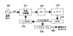
従来、基準クロックの周波数を逓倍したクロックを得るには、VCO(電圧制御発振器)を用いたPLL(フェーズロックドループ)を使用していた。図5はこのようなPLLを使用した従来のクロック逓倍回路の構成を示すブロック図である。
【0003】
図5において、501は基準クロック、502は逓倍クロック出力、511は位相比較器、512はチャージポンプ、513はローパスフィルタ、514はVCO、515は分周器、516は波形整形回路である。
【0004】
位相比較器511に入力される基準クロック501は、VCO514の出力をN分周する分周器515の出力と比較され、その位相差出力からチャージポンプ512とローパスフィルタ513により生成される制御電圧がVCO514に与えられ、これが基準クロック501のN倍の周波数を発振するように設定されたVCO514を制御することで、PLLのループ制御がなされる。波形整形回路516はVCO514の出力波形のデューティが1/2になるように波形整形を行う。
【0005】
【発明が解決しようとする課題】
しかしながら、上記従来のクロック逓倍回路には2つの大きな問題点が挙げられる。その1は、従来のクロック逓倍回路では、所望の逓倍周波数を安定させるためにローパスフィルタの時定数を大きく取る必要があり、このローパスフィルタをLSIに内蔵するときにアナログ素子である抵抗あるいは容量の値を大きくする必要がある。これらのアナログ素子分の面積増加によるチップサイズの増加あるいは抵抗や容量のばらつきにより、PLLがロックせずに発振してしまう可能性があった。
【0006】
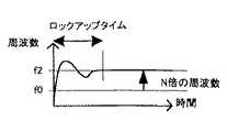
その2は、PLLは安定した発振周波数を得るためにロックアップタイムが必要なことである。図6は従来のPLLを使用したクロック逓倍回路の出力周波数の動作開始時における遷移状況を示す図である。図6に示すように、従来のPLLを使用したクロック逓倍回路では、安定した発振周波数が得られるまでに、動作時間の無駄と消費電流の無駄が生じることが避けられなかった。
【0007】
本発明は上記事情に鑑みてなされたもので、PLLのようにアナログ素子を使用せずに基準クロックから周波数を逓倍したクロックを発生し、安定した周波数が得られるクロック逓倍回路を提供することを目的とする。
【0008】
【課題を解決するための手段】
この課題を解決するために、本発明の請求項1に係るクロック逓倍回路は、基準クロックに対して外部より与えられた逓倍率の周波数を有する逓倍クロックを出力するクロック逓倍回路であって、前記逓倍クロックの周波数に比べて十分高い周波数で発振するリングオシレータと、基準クロックの半周期のカウント値を得るためにリングオシレータの出力クロックによる基準クロックのサンプリング出力をカウントする基準クロックカウンタと、得られた基準クロックの半周期のカウント値を前記逓倍率で除した値を逓倍カウント値と定義するときに、リングオシレータの出力クロックにより前記逓倍カウント値をカウントする度に逓倍クロックの出力を反転させる逓倍クロックカウンタと、を具備するものである。
【0009】
上記構成によれば、アナログ素子を用いず、逓倍カウント値をカウントする回路で逓倍クロックを生成することにより、フィードバックループの無いクロック逓倍回路が構成できるため、PLLのような過渡応答の無い出力が得られる。
【0010】
また、フリーラン動作のリングオシレータの出力クロックを用いて基準クロックの半周期のカウント値を得、同じリングオシレータの出力クロックを用いて逓倍カウント値をカウントすることにより逓倍クロックを生成しているため、リングオシレータの発振周波数が電源電圧変動や温度変動により変動しても、その変動に応じた補正が自動的に行われる。
【0011】
本発明の請求項2に係るクロック逓倍回路は、請求項1記載のクロック逓倍回路において、リングオシレータは奇数段のインバータを用いて構成されるものである。
【0012】
上記構成によれば、リングオシレータは奇数段のインバータで実現されているため、VCO等を用いた場合に必要となる発振周波数制御電圧範囲(ダイナミックレンジ)を必要とせず、回路の低電圧化が容易となる。
【0013】
本発明の請求項3に係るクロック逓倍回路は、請求項1または2記載のクロック逓倍回路において、前記逓倍クロックカウンタは基準クロックの半周期毎の反転に同期してカウントを開始するものである。
【0014】
上記構成によれば、基準クロックの半周期毎の反転に同期して逓倍クロックを生成するためのカウントを開始するため、位相比較器を用いずに逓倍クロックの位相を基順クロックの位相を揃えることができる。
【0015】
本発明の請求項4に係るクロック逓倍回路は、請求項1から3のいずれか1項記載のクロック逓倍回路において、さらにアンロック検出回路を具備し、前記逓倍クロックカウンタは前記逓倍カウント値をカウントする度にカウント終了パルスを発生させ、アンロック検出回路は基準クロックの1周期内にカウント終了パルスが検出されなかった場合にアンロック検出と判定し、このアンロック検出の判定によりリングオシレータを再起動させるものである。
【0016】
上記構成によれば、基準クロックの1周期内にカウント終了パルスが検出されなかった場合にアンロック検出を判定することにより、リングオシレータが停止したために逓倍クロックが得られない場合を検出することができ、このアンロック検出判定によりリングオシレータを再起動させることで、クロック逓倍回路の動作を自動復帰させることができる。
【0017】
【発明の実施の形態】
以下、本発明の実施の形態について図面を参照しながら説明する。
図1は本発明の一実施の形態に係るクロック逓倍回路の構成を示すブロック図である。図1において、101は基準クロック、102は逓倍クロック出力、103は逓倍率入力、104はアンロック検出出力、111はリングオシレータ、112は基準クロックカウンタ、113は逓倍率設定回路、114は逓倍クロックカウンタ、115はアンロック検出回路、116は復帰回路である。
【0018】
リングオシレータ111は、基準クロックおよび逓倍クロックに比べて十分高い周波数のクロックを発振する回路であるが、精度を必要としないため奇数段のインバータを接続して簡易に実現することが可能である。図2は、奇数段のインバータを接続したリングオシレータの構成例を示す回路図である。図2において、201はリセット信号、202は復帰パルスS4、211および212〜215はインバータ、216は起動パルス印加回路、217はOR回路である。
【0019】
また、図3は図2のリングオシレータ111の動作を説明するタイミング図である。図3に示すように、リセット信号201が入力している間はインバータ211の出力がLレベルに固定されるため、リングオシレータ111は動作を停止している。
【0020】
リセット信号201がLレベルになると、奇数段のインバータの遅延時間で決まる発振周波数でリングオシレータ111が動作を開始する。奇数段のインバータの入出力が中間電位となった場合に想定されるリングオシレータ111の発振停止に対しては、復帰パルスS4をOR回路217を介して起動パルス印加回路216に印加することにより、リングオシレータ111を再起動させるようにしている。
【0021】
図4は、以上のように構成されたクロック逓倍回路の動作を説明するタイミング図である。以下、図1から4を参照して本実施例のクロック逓倍回路の動作を説明する。ここで説明のために、リングオシレータ111の発振周波数f1を約20MHz、基準クロック101の周波数f0を1MHz、逓倍クロック102の周波数f2を2MHz、すなわち逓倍率N=2と仮定する。
【0022】
まず、基準クロックカウンタ112において、基準クロック101をリングオシレータ111の出力クロックf1でサンプリングし、基準クロック101が反転するまでのサンプリングパルスをカウントすることにより、基準クロック101の半周期のサンプリング値M=10を得る。
【0023】
ここで、サンプリング動作においては、ハザードが生じないようにリングオシレータ111の出力クロックに同期して基準クロック101の変化点を捉えるようにする。例えば、リングオシレータ111の出力クロックの立下りで基準クロック101の変化点を捉え、立ち上がりで基準クロックカウンタ112を動作させる。
【0024】
逓倍率設定回路113は、基準クロック101の半周期のサンプリング値M=10と、逓倍率入力により与えられる逓倍率N=2により、逓倍カウント値M/N=5を算出する。この逓倍カウント値M/Nは、最新の値が常時逓倍クロックカウンタ114に入力されるようにする。
【0025】
逓倍クロックカウンタ114は、基準クロック101をリングオシレータ111の出力クロックf1でサンプリングして基準クロック101が反転する変化点を捉え、この変化点を起点にしてリングオシレータ111の出力クロックf1でカウントし、逓倍カウント値M/Nまでカウントする度に出力を反転させることにより、半周期が基準クロック101の1/N、すなわち周波数f2が基準クロックの周波数f1のN倍の逓倍クロック102を生成する。
【0026】
ここでサンプリング動作においては、基準クロックカウンタ112の場合と同様に、ハザードが生じないようにリングオシレータ111の出力クロックに同期して基準クロック101の変化点を捉えるようにする。例えば、リングオシレータ111の出力クロックの立下りで基準クロック101の変化点を捉え、立ち上がりで逓倍クロックカウンタ114を動作させる。
【0027】
アンロック検出回路115には、基準クロック101の各周期で出力されるパルスS1と、逓倍クロックカウンタ114からは逓倍カウント値M/Nまでカウントしたことを示すカウント終了パルスS2とが与えられ、カウント終了パルスS2が基準クロック毎に発生しなかった場合に、これをアンロックとして検出する。
【0028】
アンロック検出回路115は、例えば、パルスS1でセットされカウント終了パルスS2でリセットされるフリップフロップを設け、パルスS1の入力時にフリップフロップがセットされていた場合に、これをアンロックとして検出することで、容易に実現することができる。
【0029】
復帰回路116はアンロック検出回路115の出力の変化を受けて、微分回路等により復帰パルスS4を発生させ、これをリングオシレータ111に印加することで、リングオシレータ111を再起動させることができ、(アンロックの原因がリングオシレータの停止による場合は)復帰が可能となる。
【0030】
以上の動作において、基準クロックカウンタ112では、リングオシレータ111の出力クロックを用いて基準クロック101の変化点を捉えて半周期のサンプリング値Mを得、逓倍クロックカウンタ114では、同じリングオシレータ111の出力クロックを用いて逓倍カウント値M/Nまでカウントしているため、リングオシレータ111の発振周波数f1が変動しても、その変動に応じた補正が自動的に行われることになる。
【0031】
これを図4により説明すると、時刻t1においてはサンプリング値M=10が得られるため、逓倍カウント値M/N=5が算出され、逓倍クロック102(f2)はリングオシレータの出力クロックf1の5パルス毎に反転しているが、時刻t2においてはリングオシレータ111の発振周波数f1が変動し、サンプリング値M=7となるため、逓倍カウント値M/N=3が算出され、逓倍クロック102(f2)はリングオシレータの出力クロックf1の3パルス毎に反転することになり、最後の半周期は位相誤差を含む波形となる。
【0032】
また、逓倍クロックカウンタ114において、基準クロック101の変化点を起点にしてリングオシレータ111の出力クロックf1でカウントすることにより、生成される逓倍クロック102の位相を基準クロック101に合わせることができる。直接位相同期を行う方法ではないため、PLLに比べて逓倍クロック1パルス毎の精度は劣るが、基準クロック周期毎に時間を合わせることが可能であり、簡易に位相を同期させたN倍のクロックを生成することができる。
【0033】
【発明の効果】
以上説明したように、本発明によれば、逓倍カウント値をカウントする回路で逓倍クロックを生成することにより、アナログ素子を用いないためLSIのチップサイズを小さくすることができ、また、フィードバックループの無いクロック逓倍回路が構成できるため、PLLのような過渡応答の無い出力が得られる。
【0034】
さらに本発明によれば、フリーラン動作のリングオシレータの出力クロックを用いて基準クロックの半周期のカウント値を得、同じリングオシレータの出力クロックを用いて逓倍カウント値をカウントすることにより逓倍クロックを生成しているため、リングオシレータの発振周波数が電源電圧変動や温度変動により変動しても、その変動に応じた補正が自動的に行われるという優れた効果が得られる。
【0035】
さらに本発明によれば、リングオシレータは奇数段のインバータで実現されているため、アナログ素子を用いた回路に比べて回路設計が容易であり、VCO等を用いた場合に必要となる発振周波数制御電圧範囲(ダイナミックレンジ)を必要とせず、回路の低電圧化が容易となるという優れた効果が得られる。
【0036】
さらに本発明によれば、基準クロックの半周期毎の反転に同期して逓倍クロックを生成するためのカウントを開始するため、位相比較器を用いずに逓倍クロックの位相を基順クロックの位相に揃えることができる。
【0037】
さらに本発明によれば、基準クロックの1周期内にカウント終了パルスが検出されなかった場合にアンロック検出を判定することにより、リングオシレータが停止したために逓倍クロックが得られない場合を検出することができ、このアンロック検出判定によりリングオシレータを再起動させることで、クロック逓倍回路の動作を自動復帰させることができるという優れた効果が得られる。
【図面の簡単な説明】
【図1】本発明の一実施の形態に係るクロック逓倍回路の構成を示すブロック図。
【図2】奇数段のインバータを接続したリングオシレータの構成を示す回路図。
【図3】奇数段のインバータを接続したリングオシレータの動作を説明するタイミング図。
【図4】本発明の一実施の形態に係るクロック逓倍回路の動作を説明するタイミング図。
【図5】従来のPLLを使用したクロック逓倍回路の構成を示すブロック図。
【図6】従来のPLLを使用したクロック逓倍回路の出力周波数の動作開始時における遷移状況を示す図。
【符号の説明】
101 基準クロック
102 逓倍クロック出力
103 逓倍率入力
104 アンロック検出出力
111 リングオシレータ
112 基準クロックカウンタ
113 逓倍率設定回路
114 逓倍クロックカウンタ
115 アンロック検出回路
116 復帰回路
201 リセット信号
202 復帰パルス
211〜215 インバータ
216 起動パルス印加回路
217 OR回路
501 基準クロック
502 逓倍クロック出力
511 位相比較器
512 チャージポンプ
513 ローパスフィルタ
514 VCO
515 分周器
516 波形整形回路[0001]
BACKGROUND OF THE INVENTION
The present invention relates to a clock multiplier circuit that generates a clock having a frequency multiplied from a reference clock.
[0002]
[Prior art]
Conventionally, in order to obtain a clock obtained by multiplying the frequency of the reference clock, a PLL (phase locked loop) using a VCO (voltage controlled oscillator) has been used. FIG. 5 is a block diagram showing a configuration of a conventional clock multiplication circuit using such a PLL.
[0003]
In FIG. 5, 501 is a reference clock, 502 is a multiplied clock output, 511 is a phase comparator, 512 is a charge pump, 513 is a low-pass filter, 514 is a VCO, 515 is a frequency divider, and 516 is a waveform shaping circuit.
[0004]
The
[0005]
[Problems to be solved by the invention]
However, there are two major problems with the conventional clock multiplication circuit. First, in a conventional clock multiplier circuit, it is necessary to increase the time constant of a low-pass filter in order to stabilize a desired multiplication frequency. When this low-pass filter is built in an LSI, the resistance or capacitance of an analog element is required. It is necessary to increase the value. There is a possibility that the PLL may oscillate without being locked due to an increase in chip size due to an increase in the area of these analog elements or variations in resistance and capacitance.
[0006]
Second, the PLL requires a lock-up time in order to obtain a stable oscillation frequency. FIG. 6 is a diagram showing a transition state at the start of operation of the output frequency of the clock multiplier circuit using the conventional PLL. As shown in FIG. 6, in the clock multiplication circuit using the conventional PLL, it is inevitable that the operation time and the consumption current are wasted until a stable oscillation frequency is obtained.
[0007]
The present invention has been made in view of the above circumstances, and provides a clock multiplier circuit that generates a clock frequency multiplied from a reference clock without using an analog element such as a PLL and obtains a stable frequency. Objective.
[0008]
[Means for Solving the Problems]
In order to solve this problem, a clock multiplication circuit according to
[0009]
According to the above configuration, a clock multiplication circuit without a feedback loop can be configured by generating a multiplication clock with a circuit that counts the multiplication count value without using an analog element, so that an output without a transient response such as a PLL is generated. can get.
[0010]
In addition, the half clock cycle count value of the reference clock is obtained using the output clock of the free-running ring oscillator, and the multiplied clock is generated by counting the multiplied count value using the same ring oscillator output clock. Even if the oscillation frequency of the ring oscillator fluctuates due to power supply voltage fluctuation or temperature fluctuation, correction according to the fluctuation is automatically performed.
[0011]
A clock multiplier circuit according to a second aspect of the present invention is the clock multiplier circuit according to the first aspect, wherein the ring oscillator includes an odd number of inverters.
[0012]
According to the above configuration, since the ring oscillator is realized by an odd number of stages of inverters, the oscillation frequency control voltage range (dynamic range) required when using a VCO or the like is not required, and the circuit voltage can be reduced. It becomes easy.
[0013]
A clock multiplier circuit according to a third aspect of the present invention is the clock multiplier circuit according to the first or second aspect, wherein the multiplied clock counter starts counting in synchronization with inversion every half cycle of the reference clock.
[0014]
According to the above configuration, in order to start counting for generating the multiplied clock in synchronization with the inversion of each half cycle of the reference clock, the phase of the multiplied clock is aligned with the phase of the base clock without using the phase comparator. be able to.
[0015]
A clock multiplication circuit according to a fourth aspect of the present invention is the clock multiplication circuit according to any one of the first to third aspects, further comprising an unlock detection circuit, wherein the multiplication clock counter counts the multiplication count value. Each time, a count end pulse is generated, and the unlock detection circuit determines that unlock is detected when the count end pulse is not detected within one cycle of the reference clock, and the ring oscillator is restarted by this unlock detection determination. It is what is started.
[0016]
According to the above configuration, by detecting the unlock detection when the count end pulse is not detected within one cycle of the reference clock, it is possible to detect the case where the multiplied clock cannot be obtained because the ring oscillator has stopped. The operation of the clock multiplier circuit can be automatically restored by restarting the ring oscillator based on the unlock detection determination.
[0017]
DETAILED DESCRIPTION OF THE INVENTION
Hereinafter, embodiments of the present invention will be described with reference to the drawings.
FIG. 1 is a block diagram showing a configuration of a clock multiplier circuit according to an embodiment of the present invention. In FIG. 1, 101 is a reference clock, 102 is a multiplication clock output, 103 is a multiplication ratio input, 104 is an unlock detection output, 111 is a ring oscillator, 112 is a reference clock counter, 113 is a multiplication ratio setting circuit, and 114 is a multiplication clock. A counter, 115 is an unlock detection circuit, and 116 is a return circuit.
[0018]
The
[0019]
FIG. 3 is a timing chart for explaining the operation of the
[0020]
When the
[0021]
FIG. 4 is a timing chart for explaining the operation of the clock multiplication circuit configured as described above. The operation of the clock multiplication circuit of this embodiment will be described below with reference to FIGS. Here, for the sake of explanation, it is assumed that the oscillation frequency f1 of the
[0022]
First, the reference clock counter 112 samples the
[0023]
Here, in the sampling operation, the change point of the
[0024]
The multiplication
[0025]
The multiplying clock counter 114 samples the
[0026]
Here, in the sampling operation, as in the case of the
[0027]
The
[0028]
The
[0029]
The
[0030]
In the above operation, the
[0031]
This will be described with reference to FIG. 4. Since the sampling value M = 10 is obtained at time t1, the multiplication count value M / N = 5 is calculated, and the multiplication clock 102 (f2) is the five pulses of the output clock f1 of the ring oscillator. However, since the oscillation frequency f1 of the
[0032]
Further, in the multiplied
[0033]
【The invention's effect】
As described above, according to the present invention, the multiplication clock is generated by the circuit that counts the multiplication count value, so that the analog chip is not used and the chip size of the LSI can be reduced. Since no clock multiplication circuit can be configured, an output without a transient response such as a PLL can be obtained.
[0034]
Furthermore, according to the present invention, a half clock cycle count value of the reference clock is obtained using the output clock of the free-running ring oscillator, and the multiplied clock value is obtained by counting the multiplied count value using the same ring oscillator output clock. Therefore, even if the oscillation frequency of the ring oscillator fluctuates due to power supply voltage fluctuations or temperature fluctuations, an excellent effect is obtained that correction according to the fluctuations is automatically performed.
[0035]
Further, according to the present invention, the ring oscillator is realized by an odd number of stages of inverters, so that the circuit design is easier than a circuit using analog elements, and the oscillation frequency control required when using a VCO or the like is required. There is no need for a voltage range (dynamic range), and an excellent effect of facilitating circuit voltage reduction is obtained.
[0036]
Furthermore, according to the present invention, in order to start counting for generating the multiplied clock in synchronization with the inversion of the reference clock every half cycle, the phase of the multiplied clock is changed to the phase of the base clock without using the phase comparator. Can be aligned.
[0037]
Furthermore, according to the present invention, by detecting the unlock detection when the count end pulse is not detected within one cycle of the reference clock, the case where the multiplied clock cannot be obtained because the ring oscillator has stopped is detected. Thus, by restarting the ring oscillator by this unlock detection determination, it is possible to obtain an excellent effect that the operation of the clock multiplier circuit can be automatically restored.
[Brief description of the drawings]
FIG. 1 is a block diagram showing a configuration of a clock multiplication circuit according to an embodiment of the present invention.
FIG. 2 is a circuit diagram showing a configuration of a ring oscillator to which an odd number of inverters are connected.
FIG. 3 is a timing chart for explaining the operation of a ring oscillator to which an odd number of inverters are connected.
FIG. 4 is a timing chart for explaining the operation of the clock multiplication circuit according to the embodiment of the present invention.
FIG. 5 is a block diagram showing a configuration of a clock multiplier circuit using a conventional PLL.
FIG. 6 is a diagram showing a transition state at the start of operation of an output frequency of a clock multiplier circuit using a conventional PLL.
[Explanation of symbols]
101
515
Claims (4)
Translated fromJapanese前記逓倍クロックの周波数に比べて十分高い周波数で発振するリングオシレータと、
前記リングオシレータの出力クロックによる前記基準クロックのサンプリング出力をカウントし前記基準クロックの半周期のカウント値を得る基準クロックカウンタと、
前記基準クロックの半周期のカウント値を前記逓倍率で除した値を逓倍カウント値として前記リングオシレータの出力クロックにより前記逓倍カウント値をカウントする度に前記逓倍クロックの出力を反転させる逓倍クロックカウンタと、を具備することを特徴とするクロック逓倍回路。A clock multiplier circuit that outputs a multiplied clock having a frequency of a multiplication ratio given from the outside with respect to a reference clock,
A ring oscillator that oscillates at a frequency sufficiently higher than the frequency of the multiplied clock;
A reference clock counter that counts the sampling output of the reference clock by the output clock of the ring oscillator and obtains a count value of a half cycle of the reference clock;
A multiplication clock counter that inverts the output of the multiplication clock every time the multiplication count value is counted by the output clock of the ring oscillator, using a value obtained by dividing the half cycle count value of the reference clock by the multiplication ratio as a multiplication count value; A clock multiplier circuit comprising:
Priority Applications (3)
| Application Number | Priority Date | Filing Date | Title |
|---|---|---|---|
| JP2002214268AJP3995552B2 (en) | 2002-07-23 | 2002-07-23 | Clock multiplier circuit |
| US10/624,904US6876236B2 (en) | 2002-07-23 | 2003-07-23 | Clock multiplier circuit |
| CN03133042.8ACN1198190C (en) | 2002-07-23 | 2003-07-23 | Clock multiple circuit |
Applications Claiming Priority (1)
| Application Number | Priority Date | Filing Date | Title |
|---|---|---|---|
| JP2002214268AJP3995552B2 (en) | 2002-07-23 | 2002-07-23 | Clock multiplier circuit |
Publications (2)
| Publication Number | Publication Date |
|---|---|
| JP2004056663A JP2004056663A (en) | 2004-02-19 |
| JP3995552B2true JP3995552B2 (en) | 2007-10-24 |
Family
ID=31936639
Family Applications (1)
| Application Number | Title | Priority Date | Filing Date |
|---|---|---|---|
| JP2002214268AExpired - Fee RelatedJP3995552B2 (en) | 2002-07-23 | 2002-07-23 | Clock multiplier circuit |
Country Status (3)
| Country | Link |
|---|---|
| US (1) | US6876236B2 (en) |
| JP (1) | JP3995552B2 (en) |
| CN (1) | CN1198190C (en) |
Families Citing this family (13)
| Publication number | Priority date | Publication date | Assignee | Title |
|---|---|---|---|---|
| AUPQ056099A0 (en)* | 1999-05-25 | 1999-06-17 | Silverbrook Research Pty Ltd | A method and apparatus (pprint01) |
| TWI245178B (en)* | 2004-01-16 | 2005-12-11 | Realtek Semiconductor Corp | Clock generation method and apparatus |
| JP2006060699A (en)* | 2004-08-23 | 2006-03-02 | Toshiba Corp | Signal processing device |
| US7132863B2 (en)* | 2005-04-04 | 2006-11-07 | Freescale Semiconductor, Inc. | Digital clock frequency doubler |
| US7394299B2 (en)* | 2005-10-06 | 2008-07-01 | Freescale Semiconductor, Inc. | Digital clock frequency multiplier |
| US7577231B2 (en)* | 2007-03-16 | 2009-08-18 | International Business Machines Corporation | Clock multiplier structure for fixed speed testing of integrated circuits |
| EP2455830A1 (en)* | 2010-11-23 | 2012-05-23 | Siemens Aktiengesellschaft | Method for recording changes in entry signals |
| KR101756944B1 (en)* | 2011-07-01 | 2017-07-12 | 페어차일드코리아반도체 주식회사 | Clock signal generation circuit and power supply device comprising the same |
| CN103595378B (en)* | 2013-11-14 | 2016-01-13 | 上海质尊溯源电子科技有限公司 | The high performance electrify restoration circuit of a kind of super low-power consumption |
| JP6300371B2 (en)* | 2014-11-20 | 2018-03-28 | ミネベアミツミ株式会社 | Motor drive control device and motor drive control method |
| KR20170022457A (en)* | 2015-08-20 | 2017-03-02 | 에스케이하이닉스 주식회사 | Period signal generation circuit and semiconductor system including the same |
| US9960771B2 (en)* | 2016-03-31 | 2018-05-01 | Wave Computing, Inc. | Hum generation using representative circuitry |
| US10461723B2 (en)* | 2017-11-30 | 2019-10-29 | Taiwan Semiconductor Manufacturing Co., Ltd. | Full range realignment ring oscillator |
Family Cites Families (18)
| Publication number | Priority date | Publication date | Assignee | Title |
|---|---|---|---|---|
| US5038117A (en)* | 1990-01-23 | 1991-08-06 | Hewlett-Packard Company | Multiple-modulator fractional-N divider |
| JPH06188898A (en) | 1992-12-16 | 1994-07-08 | Fujitsu Ltd | Clock multiplaying system |
| US5561692A (en)* | 1993-12-09 | 1996-10-01 | Northern Telecom Limited | Clock phase shifting method and apparatus |
| US5553100A (en)* | 1994-04-01 | 1996-09-03 | National Semiconductor Corporation | Fully digital data separator and frequency multiplier |
| JP3986572B2 (en)* | 1995-03-23 | 2007-10-03 | 株式会社デンソー | Frequency multiplier |
| KR0176092B1 (en) | 1995-12-20 | 1999-04-01 | 양승택 | Frequency multiplier of clock input signal |
| US5719510A (en)* | 1996-03-27 | 1998-02-17 | Intel Corporation | Software configurable digital clock generator |
| US5786715A (en)* | 1996-06-21 | 1998-07-28 | Sun Microsystems, Inc. | Programmable digital frequency multiplier |
| US6130566A (en)* | 1996-10-30 | 2000-10-10 | Yokomizo; Akira | Digital wave shaping circuit, frequency multiplying circuit, and external synchronizing method, and external synchronizing circuit |
| ES2124667B1 (en)* | 1996-12-16 | 1999-06-16 | Telefonica Nacional Espana Co | INTEGRATED FREQUENCY MULTIPLIER CIRCUIT. |
| US5815043A (en)* | 1997-02-13 | 1998-09-29 | Apple Computer, Inc. | Frequency controlled ring oscillator having by passable stages |
| US5854576A (en)* | 1997-04-21 | 1998-12-29 | Ati Technologies | Method and apparatus for a finely adjustable clock circuit |
| JPH10322174A (en) | 1997-05-21 | 1998-12-04 | Oki Micro Design Miyazaki:Kk | Frequency-multiplying circuit |
| JP3110377B2 (en)* | 1998-04-28 | 2000-11-20 | 日本電気アイシーマイコンシステム株式会社 | Multiplier circuit |
| DE19946494A1 (en)* | 1999-09-28 | 2001-05-03 | Infineon Technologies Ag | Receiver for different frequency bands |
| JP2001127598A (en)* | 1999-10-29 | 2001-05-11 | Oki Micro Design Co Ltd | Frequency multiplying circuit |
| US6329850B1 (en)* | 1999-12-27 | 2001-12-11 | Texas Instruments Incorporated | Precision frequency and phase synthesis |
| US6509800B2 (en)* | 2001-04-03 | 2003-01-21 | Agilent Technologies, Inc. | Polyphase noise-shaping fractional-N frequency synthesizer |
- 2002
- 2002-07-23JPJP2002214268Apatent/JP3995552B2/ennot_activeExpired - Fee Related
- 2003
- 2003-07-23USUS10/624,904patent/US6876236B2/ennot_activeExpired - Fee Related
- 2003-07-23CNCN03133042.8Apatent/CN1198190C/ennot_activeExpired - Fee Related
Also Published As
| Publication number | Publication date |
|---|---|
| US20040135601A1 (en) | 2004-07-15 |
| JP2004056663A (en) | 2004-02-19 |
| US6876236B2 (en) | 2005-04-05 |
| CN1479186A (en) | 2004-03-03 |
| CN1198190C (en) | 2005-04-20 |
Similar Documents
| Publication | Publication Date | Title |
|---|---|---|
| TWI404073B (en) | Digital-to-time converter and digital-to-time converting method | |
| JP3995552B2 (en) | Clock multiplier circuit | |
| TWI685206B (en) | Phase-locked loop circuit | |
| JP2011040943A (en) | Phase-locked loop circuit | |
| JP2005065283A (en) | Phase lock loop and method for detecting lock situation in phase lock loop | |
| CN115765728B (en) | Phase frequency detector and phase-locked loop | |
| JP2006119123A (en) | Phase difference detection device | |
| US7250803B2 (en) | PLL output clock stabilization circuit | |
| KR20190081415A (en) | Injection locked frequency multiplier and method for multiplying frequency thereof | |
| JPH0783262B2 (en) | Synthesizer device | |
| JP2811994B2 (en) | Phase locked loop | |
| JP6453541B2 (en) | Clock generation circuit | |
| JP6158012B2 (en) | Clock phase shift circuit | |
| JPH08274629A (en) | Digital PLL circuit | |
| CN113193868A (en) | Phase-locked detection device, phase-locked detection method and phase-locked loop | |
| JP3079943B2 (en) | PLL circuit | |
| US6177821B1 (en) | Microcomputer with frequency multiplication circuit | |
| JPH05259900A (en) | Phase modulation circuit | |
| CN215186702U (en) | Phase-locked detection device and phase-locked loop | |
| JPH06101677B2 (en) | Timer-circuit | |
| JP2004080123A (en) | Phase lock oscillation circuit | |
| JP2009231959A (en) | Pll circuit | |
| JP2002305444A (en) | PLL circuit | |
| JP3263200B2 (en) | Synchronous signal generation circuit and frequency division circuit | |
| KR940006093Y1 (en) | Digital phase locked loop circuit |
Legal Events
| Date | Code | Title | Description |
|---|---|---|---|
| A621 | Written request for application examination | Free format text:JAPANESE INTERMEDIATE CODE: A621 Effective date:20050711 | |
| RD04 | Notification of resignation of power of attorney | Free format text:JAPANESE INTERMEDIATE CODE: A7424 Effective date:20060325 | |
| A977 | Report on retrieval | Free format text:JAPANESE INTERMEDIATE CODE: A971007 Effective date:20070531 | |
| TRDD | Decision of grant or rejection written | ||
| A01 | Written decision to grant a patent or to grant a registration (utility model) | Free format text:JAPANESE INTERMEDIATE CODE: A01 Effective date:20070704 | |
| A61 | First payment of annual fees (during grant procedure) | Free format text:JAPANESE INTERMEDIATE CODE: A61 Effective date:20070731 | |
| FPAY | Renewal fee payment (event date is renewal date of database) | Free format text:PAYMENT UNTIL: 20100810 Year of fee payment:3 | |
| R150 | Certificate of patent or registration of utility model | Free format text:JAPANESE INTERMEDIATE CODE: R150 | |
| FPAY | Renewal fee payment (event date is renewal date of database) | Free format text:PAYMENT UNTIL: 20100810 Year of fee payment:3 | |
| FPAY | Renewal fee payment (event date is renewal date of database) | Free format text:PAYMENT UNTIL: 20110810 Year of fee payment:4 | |
| FPAY | Renewal fee payment (event date is renewal date of database) | Free format text:PAYMENT UNTIL: 20110810 Year of fee payment:4 | |
| FPAY | Renewal fee payment (event date is renewal date of database) | Free format text:PAYMENT UNTIL: 20120810 Year of fee payment:5 | |
| LAPS | Cancellation because of no payment of annual fees |