JP3993000B2 - Setting method of retardation of liquid crystal display device - Google Patents
Setting method of retardation of liquid crystal display deviceDownload PDFInfo
- Publication number
- JP3993000B2 JP3993000B2JP2002064481AJP2002064481AJP3993000B2JP 3993000 B2JP3993000 B2JP 3993000B2JP 2002064481 AJP2002064481 AJP 2002064481AJP 2002064481 AJP2002064481 AJP 2002064481AJP 3993000 B2JP3993000 B2JP 3993000B2
- Authority
- JP
- Japan
- Prior art keywords
- retardation
- liquid crystal
- film
- rlc
- display device
- Prior art date
- Legal status (The legal status is an assumption and is not a legal conclusion. Google has not performed a legal analysis and makes no representation as to the accuracy of the status listed.)
- Expired - Fee Related
Links
Images


Classifications
- G—PHYSICS
- G02—OPTICS
- G02F—OPTICAL DEVICES OR ARRANGEMENTS FOR THE CONTROL OF LIGHT BY MODIFICATION OF THE OPTICAL PROPERTIES OF THE MEDIA OF THE ELEMENTS INVOLVED THEREIN; NON-LINEAR OPTICS; FREQUENCY-CHANGING OF LIGHT; OPTICAL LOGIC ELEMENTS; OPTICAL ANALOGUE/DIGITAL CONVERTERS
- G02F1/00—Devices or arrangements for the control of the intensity, colour, phase, polarisation or direction of light arriving from an independent light source, e.g. switching, gating or modulating; Non-linear optics
- G02F1/01—Devices or arrangements for the control of the intensity, colour, phase, polarisation or direction of light arriving from an independent light source, e.g. switching, gating or modulating; Non-linear optics for the control of the intensity, phase, polarisation or colour
- G02F1/13—Devices or arrangements for the control of the intensity, colour, phase, polarisation or direction of light arriving from an independent light source, e.g. switching, gating or modulating; Non-linear optics for the control of the intensity, phase, polarisation or colour based on liquid crystals, e.g. single liquid crystal display cells
- G02F1/133—Constructional arrangements; Operation of liquid crystal cells; Circuit arrangements
- G02F1/1333—Constructional arrangements; Manufacturing methods
- G02F1/1335—Structural association of cells with optical devices, e.g. polarisers or reflectors
- G02F1/13363—Birefringent elements, e.g. for optical compensation
- G02F1/133634—Birefringent elements, e.g. for optical compensation the refractive index Nz perpendicular to the element surface being different from in-plane refractive indices Nx and Ny, e.g. biaxial or with normal optical axis
- G—PHYSICS
- G02—OPTICS
- G02F—OPTICAL DEVICES OR ARRANGEMENTS FOR THE CONTROL OF LIGHT BY MODIFICATION OF THE OPTICAL PROPERTIES OF THE MEDIA OF THE ELEMENTS INVOLVED THEREIN; NON-LINEAR OPTICS; FREQUENCY-CHANGING OF LIGHT; OPTICAL LOGIC ELEMENTS; OPTICAL ANALOGUE/DIGITAL CONVERTERS
- G02F1/00—Devices or arrangements for the control of the intensity, colour, phase, polarisation or direction of light arriving from an independent light source, e.g. switching, gating or modulating; Non-linear optics
- G02F1/01—Devices or arrangements for the control of the intensity, colour, phase, polarisation or direction of light arriving from an independent light source, e.g. switching, gating or modulating; Non-linear optics for the control of the intensity, phase, polarisation or colour
- G02F1/13—Devices or arrangements for the control of the intensity, colour, phase, polarisation or direction of light arriving from an independent light source, e.g. switching, gating or modulating; Non-linear optics for the control of the intensity, phase, polarisation or colour based on liquid crystals, e.g. single liquid crystal display cells
- G02F1/133—Constructional arrangements; Operation of liquid crystal cells; Circuit arrangements
- G02F1/1333—Constructional arrangements; Manufacturing methods
- G02F1/1335—Structural association of cells with optical devices, e.g. polarisers or reflectors
- G—PHYSICS
- G02—OPTICS
- G02F—OPTICAL DEVICES OR ARRANGEMENTS FOR THE CONTROL OF LIGHT BY MODIFICATION OF THE OPTICAL PROPERTIES OF THE MEDIA OF THE ELEMENTS INVOLVED THEREIN; NON-LINEAR OPTICS; FREQUENCY-CHANGING OF LIGHT; OPTICAL LOGIC ELEMENTS; OPTICAL ANALOGUE/DIGITAL CONVERTERS
- G02F1/00—Devices or arrangements for the control of the intensity, colour, phase, polarisation or direction of light arriving from an independent light source, e.g. switching, gating or modulating; Non-linear optics
- G02F1/01—Devices or arrangements for the control of the intensity, colour, phase, polarisation or direction of light arriving from an independent light source, e.g. switching, gating or modulating; Non-linear optics for the control of the intensity, phase, polarisation or colour
- G02F1/13—Devices or arrangements for the control of the intensity, colour, phase, polarisation or direction of light arriving from an independent light source, e.g. switching, gating or modulating; Non-linear optics for the control of the intensity, phase, polarisation or colour based on liquid crystals, e.g. single liquid crystal display cells
- G02F1/137—Devices or arrangements for the control of the intensity, colour, phase, polarisation or direction of light arriving from an independent light source, e.g. switching, gating or modulating; Non-linear optics for the control of the intensity, phase, polarisation or colour based on liquid crystals, e.g. single liquid crystal display cells characterised by the electro-optical or magneto-optical effect, e.g. field-induced phase transition, orientation effect, guest-host interaction or dynamic scattering
- G02F1/139—Devices or arrangements for the control of the intensity, colour, phase, polarisation or direction of light arriving from an independent light source, e.g. switching, gating or modulating; Non-linear optics for the control of the intensity, phase, polarisation or colour based on liquid crystals, e.g. single liquid crystal display cells characterised by the electro-optical or magneto-optical effect, e.g. field-induced phase transition, orientation effect, guest-host interaction or dynamic scattering based on orientation effects in which the liquid crystal remains transparent
- G02F1/1393—Devices or arrangements for the control of the intensity, colour, phase, polarisation or direction of light arriving from an independent light source, e.g. switching, gating or modulating; Non-linear optics for the control of the intensity, phase, polarisation or colour based on liquid crystals, e.g. single liquid crystal display cells characterised by the electro-optical or magneto-optical effect, e.g. field-induced phase transition, orientation effect, guest-host interaction or dynamic scattering based on orientation effects in which the liquid crystal remains transparent the birefringence of the liquid crystal being electrically controlled, e.g. ECB-, DAP-, HAN-, PI-LC cells
Landscapes
- Physics & Mathematics (AREA)
- Nonlinear Science (AREA)
- Chemical & Material Sciences (AREA)
- Crystallography & Structural Chemistry (AREA)
- General Physics & Mathematics (AREA)
- Optics & Photonics (AREA)
- Mathematical Physics (AREA)
- Liquid Crystal (AREA)
- Polarising Elements (AREA)
Abstract
Description
Translated fromJapanese【0001】
【発明の属する技術分野】
本発明は、垂直配向方式の液晶表示装置に関するものである。
【0002】
【従来の技術】
従来から、液晶表示装置は、ワードプロセッサやコンピュータの画面として広く使用されており、近年では、テレビの画面としても急速に普及している。これらの液晶表示装置の多くは、TN(Twisted Nematic)モードを採用しているが、当該液晶表示装置には、斜め方向から見たときに、コントラストが低下しやすく、階調特性が反転しやすいという問題がある。
【0003】
したがって、近年では、斜め方向からの視角特性を向上させるために、VA(Verticically Alignment)モードの液晶表示装置が注目されるようになっている。当該モードの液晶表示装置の液晶セルは、負の誘電異方性を有するネマチック液晶と垂直配向膜とを組み合わせて構成されている。
【0004】
さらに、例えば、登録特許第2947530号や特開2000−39610では、図16および図17に示すように、黒表示時における液晶セル111の光学異方性を光学的に補償するために、液晶セル111と偏光板112との間に、2軸性フィルム116を配した液晶表示装置101、あるいは、液晶セル111と偏光板112との間に正の1軸性フィルム114を配し、当該正の1軸性フィルム114と偏光板112との間に負の1軸性フィルム115を配した液晶表示装置101aが開示されている。
【0005】
上記構成では、液晶分子が垂直配向している液晶セル111を斜め方向から見た場合に、液晶セル111が極角に応じた位相差を透過光に与えているにも拘わらず、各フィルム116(114・115)のリターデーションが適切に設定されていれば、各フィルム116(114・115)によって、当該位相差が補償される。したがって、正面方向から見た場合、すなわち、液晶分子が透過光の偏光状態を維持する場合と略同様に、黒表示できる。この結果、斜め方向から見た場合の光漏れを防止でき、コントラストを向上できると共に、着色や階調つぶれの発生を抑制できる。
【0006】
【発明が解決しようとする課題】
しかしながら、今日では、さらなる広視野角、高表示品位の液晶表示装置が望まれる状況下において、斜め方向から見た場合の着色や階調つぶれの改善が要求されているが、上記の登録特許第2947530号や特開2000−39610に記載されたリターデーションの各フィルム116(114・115)を用いた場合は、必ずしも充分であるとは言えず、未だ改善の余地を残している。
【0007】
本発明は、上記した課題に鑑み、垂直配向モードの液晶表示装置において、斜め方向からの見た場合における着色や階調つぶれ抑制に適した各フィルムのリターデーションに対し、偏光板の基材フィルムが与える影響を考察した結果なされたものであって、その目的は、斜め方向から見た場合のコントラストを実用上十分高い値に維持しながら、着色や階調つぶれが実用上許容範囲内に抑えられた液晶表示装置を確実に提供することにある。
【0008】
【課題を解決するための手段】
本発明に係る液晶表示装置は、上記課題を解決するために、液晶を挟持すると共に当該液晶の液晶分子を表面に概ね垂直に配向させる2枚の基板が設けられた液晶セルと、当該液晶セルの両側に配され、それぞれの吸収軸が互いに直交するように配された2枚の偏光板と、上記両偏光板の一方および上記液晶セルの間に配され、正の1軸異方性を有する第1位相差フィルムと、当該偏光板および第1位相差フィルムの間に配され、負の1軸異方性を有する第2位相差フィルムとを備え、上記液晶は、負の誘電異方性を有していると共に、上記両偏光板には、光軸が上記基板に概ね垂直になるように配置され、負の1軸異方性を有する基材フィルムが設けられ、上記第1位相差フィルムの遅相軸は、上記液晶から見て同じ側の上記偏光板の吸収軸と直交するように配され、上記第2位相差フィルムの光軸が上記基板に概ね垂直になるように配されている液晶表示装置において、以下の手段を講じたことを特徴としている。
【0009】
すなわち、上記第1位相差フィルムの面内方向のリターデーションをRp〔nm〕、上記第2位相差フィルムの厚み方向のリターデーションをRn〔nm〕、上記基材フィルムの厚み方向のリターデーションをRtac〔nm〕、上記液晶の厚み方向のリターデーションをRlc〔nm〕とし、上記Rpに関するパラメータα〔nm〕を、α=35+(Rlc/80−4)2×3.5+(360−Rlc)×Rtac/850、上記Rnに関するパラメータβ〔nm〕を、β=Rlc−1.9×Rtacとするとき、上記リターデーションRpは、上記αの90%以上かつ110%以下の値に設定されていると共に、上記リターデーションRnは、上記βの65%以上かつ85%以下の値に設定されている。
【0010】
上記構成の液晶表示装置において、基板に概ね垂直に配向している液晶分子が基板の法線方向から入射した光に対して位相差を与えないにも拘わらず、斜めから入射した光に対しては、極角(法線方向からの傾斜角)に応じた位相差を与えてしまうので、第1および第2位相差フィルムがないと、本来、出射側の偏光板によって吸収すべき光が、完全には吸収されない。この結果、光漏れが発生して、コントラストを低下させると共に、着色や階調つぶれが発生してしまう。
【0011】
これに対して、上記構成では、上記第1および第2位相差フィルムが設けられているので、上記液晶が極角に応じて与えてしまった位相差が両位相差フィルムによって補償される。この結果、斜め方向から見た場合の光漏れを防止し、コントラストを向上すると共に、着色や階調つぶれの発生を防止できる。
【0012】
ただし、上記両位相差フィルムのリターデーションを決定する際、基材フィルムが無い場合に最適な上記第1および第2位相差フィルムが有する厚み方向のリターデーションから、上記基材フィルムが有する厚み方向のリターデーションを引き算するだけでは、斜め方向から見た場合における、着色や階調つぶれのさらなる抑制が要求される状況下では、必ずしも十分であるとは言えない。
【0013】
そこで、本願発明者は、垂直配向モードの液晶表示装置を斜め方向から見た場合におけるコントラストを実用上十分に高い値に維持したまま、着色や階調つぶれをさらに抑制すべく、研究を重ねた結果、基材フィルムの厚み方向のリターデーションは、上記第1および第2位相差フィルムの厚み方向のリターデーションと同等に作用するわけではないことを見出し、特に、正の1軸異方性を有する第1位相差フィルムの面内方向のリターデーションRpを上記コントラストが最大になるように設定する際、液晶の有するリターデーションが360〔nm〕を超えているか否かによって、上記基材フィルムの厚み方向のリターデーションに対する上記リターデーションRpの依存性が逆転すること、並びに、コントラストが最大になるような上記各リターデーションを基準に、所定の範囲に設定することによって、着色や階調つぶれを効果的に抑制できることを見出し、本発明を完成させるに至った。
【0014】
本発明の液晶表示装置では、上記基材フィルムおよび液晶の厚み方向のリターデーションRtacおよびRlcに応じ、しかも、斜め方向から見た場合のコントラストを実用上十分に高い値に維持したまま、着色や階調つぶれを許容できる範囲に、上記リターデーションRpおよびRnを設定している。これにより、基材フィルムの厚み方向のリターデーションを上記第1および第2位相差フィルムの厚み方向のリターデーションと同等に扱う場合と異なり、上記斜め方向から見た場合のコントラストが実用上十分に高い値に維持され、しかも、着色や階調つぶれが許容範囲内に抑えられた液晶表示装置を確実に得ることができる。
【0015】
また、上記着色や階調つぶれの抑制と生産性の向上との双方が特に要求される場合には、上記構成に加えて、上記液晶の厚み方向のリターデーションRlcは、342〔nm〕から378〔nm〕までの範囲に設定され、上記第1位相差フィルムの面内方向のリターデーションRpが、33.3〔nm〕から38.6〔nm〕までの範囲に設定されている方が望ましい。
【0016】
上記リターデーションRlcおよびRpが当該範囲に設定されていれば、基材フィルムに製造バラツキが発生して、基材フィルムの厚み方向のリターデーションが変化しても、上記リターデーションRpを上記αの90%〜110%の範囲に設定できる。この結果、基材フィルムの厚み方向のリターデーションにバラツキが発生する場合であっても、同じ上記第1位相差フィルムを用いることができ、生産性を向上できる。
【0017】
また、本発明に係る液晶表示装置は、液晶を挟持すると共に当該液晶の液晶分子を表面に概ね垂直に配向させる2枚の基板が設けられた液晶セルと、当該液晶セルの両側に配され、それぞれの吸収軸が互いに直交するように配された2枚の偏光板と、上記両偏光板の一方および上記液晶セルの間に配され、正の1軸異方性を有する第1位相差フィルムと、当該偏光板および第1位相差フィルムの間に配され、負の1軸異方性を有する第2位相差フィルムとを備え、上記液晶は、負の誘電異方性を有していると共に、上記両偏光板には、光軸が上記基板に概ね垂直になるように配置され、負の1軸異方性を有する基材フィルムが設けられ、上記第1位相差フィルムの遅相軸は、上記液晶から見て同じ側の上記偏光板の吸収軸と直交するように配され、上記第2位相差フィルムの光軸が上記基板に概ね垂直になるように配されている液晶表示装置において、上記第1位相差フィルムの面内方向のリターデーションをRp〔nm〕、上記第2位相差フィルムの厚み方向のリターデーションをRn〔nm〕、上記基材フィルムの厚み方向のリターデーションをRtac〔nm〕、上記液晶の厚み方向のリターデーションをRlc〔nm〕とし、上記Rpに関するパラメータα〔nm〕を、α=35+(Rlc/80−4)2×3.5+(360−Rlc)×Rtac/850 上記Rnに関するパラメータβ〔nm〕を、β=Rlc−1.9×Rtacとするとき、上記リターデーションRpは、上記αの80%以上かつ120%以下の値に設定されていると共に、上記リターデーションRnは、上記βの85%以上かつ90%以下の値に設定されていることを特徴としている。当該構成によれば、着色や階調つぶれを許容範囲内に抑え、しかも、上記液晶表示装置と比較してコントラストを向上できる。
【0018】
一方、本発明に係る液晶表示装置は、上記課題を解決するために、液晶を挟持すると共に当該液晶の液晶分子を表面に概ね垂直に配向させる2枚の基板が設けられた液晶セルと、当該液晶セルの両側に配され、それぞれの吸収軸が互いに直交するように配された2枚の偏光板と、上記両偏光板の一方および上記液晶セルの間に配され、2軸異方性を有する位相差フィルムとを備え、上記液晶は、負の誘電異方性を有していると共に、上記両偏光板には、光軸が上記基板に概ね垂直になるように配置され、負の1軸異方性を有する基材フィルムが設けられ、上記位相差フィルムの面内の遅相軸は、上記液晶から見て同じ側の上記偏光板の吸収軸と直交するように配されている液晶表示装置において、以下の手段を講じたことを特徴としている。
【0019】
すなわち、上記位相差フィルムの面内方向のリターデーションをRxy〔nm〕、上記位相差フィルムの厚み方向のリターデーションをRz〔nm〕、上記基材フィルムの厚み方向のリターデーションをRtac〔nm〕、上記液晶のあつみ方向のリターデーションをRlc〔nm〕とし、上記Rxyに関するパラメータα〔nm〕を、α=85−0.09×Rlc−Rtac/20、上記Rzに関するパラメータβ〔nm〕を、β=1.05×Rlc−1.9×Rtacとするとき、上記リターデーションRxyは、上記αの90%以上かつ110%以下の値に設定されていると共に、上記リターデーションRzは、上記βの65%以上かつ85%以下の値に設定されている。
【0020】
また、本発明に係る液晶表示装置は、上記課題を解決するために、液晶を挟持すると共に当該液晶の液晶分子を表面に概ね垂直に配向させる2枚の基板が設けられた液晶セルと、当該液晶セルの両側に配され、それぞれの吸収軸が互いに直交するように配された2枚の偏光板と、上記両偏光板の一方および上記液晶セルの間に配され、2軸異方性を有する第1位相差フィルムと、上記両偏光板の他方および上記液晶セルの間に配され、2軸異方性を有する第2位相差フィルムとを備え、上記液晶は、負の誘電異方性を有していると共に、上記両偏光板には、光軸が上記基板に概ね垂直になるように配置され、負の1軸異方性を有する基材フィルムが設けられ、上記第1および第2位相差フィルムの面内の遅相軸は、上記液晶から見て同じ側の上記偏光板の吸収軸と直交するように配されている液晶表示装置において、以下の手段を講じたことを特徴としている。
【0021】
すなわち、上記各位相差フィルムの面内方向のリターデーションをRxy〔nm〕、上記各位相差フィルムの厚み方向のリターデーションをRz〔nm〕、上記基材フィルムの厚み方向のリターデーションをRtac〔nm〕、上記液晶の厚み方向のリターデーションをRlc〔nm〕とし、上記Rxyに関するパラメータα〔nm〕を、α=42.5−0.045×Rlc−Rtac/40、上記Rzに関するパラメータβ〔nm〕を、β=0.525×Rlc−0.95×Rtacとするとき、上記第1および第2位相差フィルムのリターデーションRxyは、上記αの90%以上かつ110%以下の値に設定されていると共に、上記第1および第2位相差フィルムのリターデーションRzは、上記βの65%以上かつ85%以下の値に設定されている。
【0022】
上記各構成の液晶表示装置では、液晶分子が基板に概ね垂直に配向している状態で、液晶が斜め方向の光に与えた位相差は、上記位相差フィルム、あるいは、第1および第2位相差フィルムによって補償され、斜め方向から見た場合の光漏れを防止し、コントラストを向上できる。
【0023】
しかしながら、当該構成であっても、上記位相差フィルムあるいは第1および第2位相差フィルムのリターデーションを決定する際、基材フィルムが無い場合に最適な各位相差フィルムが有する厚み方向のリターデーションから、上記基材フィルムが有する厚み方向のリターデーションを引き算するだけでは、斜め方向から見た場合における、着色や階調つぶれのさらなる抑制が要求される状況下では、必ずしも十分であるとは言えない。
【0024】
そこで、本願発明者は、垂直配向モードの液晶表示装置を斜め方向から見た場合のコントラストをさらに向上すべく、研究を重ねた結果、上述の液晶表示装置と同様に、基材フィルムの厚み方向のリターデーションは、上記位相差フィルム、あるいは、第1および第2位相差フィルムの厚み方向のリターデーションと同等に作用するわけではないことを見出した。さらに、2軸異方性を有する面内方向のリターデーションRxyと、基材フィルムの厚み方向のリターデーションRtacとは、リターデーションの方向が互いに異なっているにも拘わらず、上記リターデーションRxyを適切に設定するためには、リターデーションRtacの影響も加味すべきこと、並びに、コントラストが最大になるような上記各リターデーションを基準に、所定の範囲に設定することによって、着色や階調つぶれを効果的に抑制できることを見出し、本発明を完成させるに至った。
【0025】
本発明の液晶表示装置では、位相差フィルム、あるいは、第1および第2位相差フィルムの面内方向のリターデーションRxyと厚み方向のリターデーションRzとを設定する際、上記液晶および基材フィルムの厚み方向のリターデーションRlcおよびRtacに応じて設定すると共に、斜め方向から見た場合のコントラストが実用上十分に高い値に維持したまま、着色や階調つぶれを許容できる範囲に、上記リターデーションRxyおよびRzを設定している。これにより、基材フィルムの厚み方向のリターデーションを、位相差フィルム、あるいは、上記第1および第2位相差フィルムの厚み方向のリターデーションと同等に扱う場合と異なり、上記斜め方向から見た場合のコントラストが実用上十分に高い値に維持され、しかも、着色や階調つぶれが許容範囲内に抑えられた液晶表示装置を確実に得ることができる。
【0026】
また、本発明に係る液晶表示装置は、液晶を挟持すると共に当該液晶の液晶分子を表面に概ね垂直に配向させる2枚の基板が設けられた液晶セルと、当該液晶セルの両側に配され、それぞれの吸収軸が互いに直交するように配された2枚の偏光板と、上記両偏光板の一方および上記液晶セルの間に配され、2軸異方性を有する位相差フィルムとを備え、上記液晶は、負の誘電異方性を有していると共に、上記両偏光板には、光軸が上記基板に概ね垂直になるように配置され、負の1軸異方性を有する基材フィルムが設けられ、上記位相差フィルムの面内の遅相軸は、上記液晶から見て同じ側の上記偏光板の吸収軸と直交するように配されている液晶表示装置において、上記位相差フィルムの面内方向のリターデーションをRxy〔nm〕、上記位相差フィルムの厚み方向のリターデーションをRz〔nm〕、上記基材フィルムの厚み方向のリターデーションをRtac〔nm〕、上記液晶の厚み方向のリターデーションをRlc〔nm〕とし、上記Rxyに関するパラメータα〔nm〕を、α=85−0.09×Rlc−Rtac/20 上記Rzに関するパラメータβ〔nm〕を、β=1.05×Rlc−1.9×Rtacとするとき、上記リターデーションRxyは、上記αの80%以上かつ120%以下の値に設定されていると共に、上記リターデーションRzは、上記βの85%以上かつ90%以下の値に設定されていることを特徴としている。当該構成によれば、着色や階調つぶれを許容範囲内に抑え、しかも、上記液晶表示装置と比較してコントラストを向上できる。
【0027】
さらに、本発明に係る液晶表示装置は、液晶を挟持すると共に当該液晶の液晶分子を表面に概ね垂直に配向させる2枚の基板が設けられた液晶セルと、当該液晶セルの両側に配され、それぞれの吸収軸が互いに直交するように配された2枚の偏光板と、上記両偏光板の一方および上記液晶セルの間に配され、2軸異方性を有する第1位相差フィルムと、上記両偏光板の他方および上記液晶セルの間に配され、2軸異方性を有する第2位相差フィルムとを備え、上記液晶は、負の誘電異方性を有していると共に、上記両偏光板には、光軸が上記基板に概ね垂直になるように配置され、負の1軸異方性を有する基材フィルムが設けられ、上記第1および第2位相差フィルムの面内の遅相軸は、上記液晶から見て同じ側の上記偏光板の吸収軸と直交するように配されている液晶表示装置において、上記各位相差フィルムの面内方向のリターデーションをRxy〔nm〕、上記各位相差フィルムの厚み方向のリターデーションをRz〔nm〕、上記基材フィルムの厚み方向のリターデーションをRtac〔nm〕、上記液晶の厚み方向のリターデーションをRlc〔nm〕とし、上記Rxyに関するパラメータα〔nm〕を、α=42.5−0.045×Rlc−Rtac/40 上記Rzに関するパラメータβ〔nm〕を、β=0.525×Rlc−0.95×Rtacとするとき、上記第1および第2位相差フィルムのリターデーションRxyは、上記αの80%以上かつ120%以下の値に設定されていると共に、上記第1および第2位相差フィルムのリターデーションRzは、上記βの85%以上かつ90%以下の値に設定されていることを特徴としている。当該構成によれば、着色や階調つぶれを許容範囲内に抑え、しかも、上記液晶表示装置と比較してコントラストを向上できる。
【0028】
さらに、本発明に係る液晶表示装置は、上記各位相差フィルムが2軸異方性を有するか否かに拘わらず、上記液晶は、負の誘電異方性を有しているので、基板に対して略垂直方向の電界を印加することによって、基板の法線方向に配向した液晶分子を電界強度に応じて傾斜させることができ、正の誘電異方性を有している場合よりも、電極の構造を簡略化できる。
【0029】
【発明の実施の形態】
〔第1の実施形態〕
本発明の一実施形態について図1ないし図7に基づいて説明すると以下の通りである。なお、詳細は後述するように、本発明は、他の液晶セルにも適用できるが、以下では、好適な一例として、マルチドメイン配向の液晶セルについて説明する。
【0030】
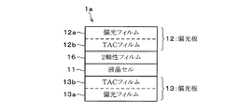
本実施形態に係る液晶表示装置1は、図1に示すように、垂直配向(VA)方式の液晶セル11と、当該液晶セル11の両側に配された偏光板12・13と、一方の偏光板12および液晶セル11の間に配された正の1軸性フィルム(第1位相差フィルム)14と、当該正の1軸性フィルム14および偏光板12の間に配された負の1軸性フィルム(第2位相差フィルム)15とを積層して構成されている。
【0031】
上記液晶セル11は、図2に示すように、画素に対応する画素電極21a(後述)が設けられたTFT(Thin Film Transistor)基板11aと、対向電極21bが設けられた対向基板11bと、両基板11a・11bにて挟持され、負の誘電異方性を有するネマチック液晶からなる液晶層11cとを備えている。なお、本実施形態に係る液晶表示装置1は、カラー表示可能であり、上記対向基板11bには、各画素の色に対応するカラーフィルタが形成されている。
【0032】
さらに、上記画素電極21aが形成されたTFT基板11aには、液晶層11c側の表面に垂直配向膜22aが形成されている。同様に、上記対向電極21bが形成された対向基板11bの液晶層11c側の表面には、垂直配向膜22bが形成されている。これにより、上記両電極21a・21b間に電圧が印加されていない状態において、両基板11a・11c間に配された液晶層11cの液晶分子Mが、上記基板11a・11b表面に対して垂直に配向する。また、両電極21a・21b間に電圧が印加されると、液晶分子Mは、上記基板11a・11bの法線方向に沿った状態(電圧無印加状態)から、印加電圧に応じた傾斜角で傾斜する(図3参照)。なお、両基板11a・11bが対向しているので、特に区別する必要がある場合を除いて、それぞれの法線方向および面内方向を、単に法線方向あるいは面内方向と称する。
【0033】
ここで、本実施形態に係る液晶セル11は、マルチドメイン配向の液晶セルであって、各画素が複数の範囲(ドメイン)に分割され、配向方向、すなわち、電圧印加時に液晶分子Mが傾斜する際の方位(傾斜角の面内成分)が、各ドメイン間で異なるように制御されている。
【0034】
具体的には、図4に示すように、上記画素電極21aには、断面形状が山型で、面内の形状がジグザグと略直角に曲がる突起列23a…が、ストライプ状に形成されている。同様に、上記対向電極21bには、法線方向の形状が山型で、面内の形状がジグザグと略直角に曲がる突起列23b…が、ストライプ状に形成されている。これらの両突起列23a・23bの面内方向における間隔は、突起列23aの斜面の法線と突起列23bの斜面の法線とが略一致するように配されている。また、上記各突起列23a・23bは、上記画素電極21aおよび対向電極21b上に感光性樹脂を塗布し、フォトリソグラフィー工程で加工することで形成されている。
【0035】
ここで、突起列23aの近傍では、液晶分子が斜面に垂直になるように配向する。加えて、電圧印加時において、突起列23aの近傍の電界は、突起列23aの斜面に平行になるように傾く。ここで、液晶分子は、長軸が電界に垂直な方向に傾き、液晶の連続性によって、突起列23aの斜面から離れた液晶分子も斜面近傍の液晶分子と同様の方向に配向する。同様にして、電圧印加時において、突起列23bの近傍の電界は、突起列23bの斜面に平行になるように傾く。ここで、液晶分子は、長軸が電界に垂直な方向に傾き、液晶の連続性によって、突起列23bの斜面から離れた液晶分子も斜面近傍の液晶分子と同様の方向に配向する。
【0036】
これらの結果、各突起列23a…および23b…において、角部C以外の部分を線部と称すると、突起列23aの線部L23aと突起列23bの線部L23bとの間の領域では、電圧印加時における液晶分子の配向方向の面内成分は、線部L23aから線部23bへの方向の面内成分と一致する。
【0037】
ここで、各突起列23a・23bは、角部Cで略直角に曲がっている。したがて、液晶分子の配向方向は、画素内で4分割され、画素内に、液晶分子の配向方向が互いに異なるドメインD1〜D4を形成できる。
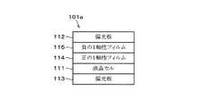
【0038】
一方、図1に示す偏光板12・13は、それぞれ、偏光フィルム12a・13bと、偏光フィルム12a・13aを保持する基材フィルムとしてのトリアセチルセルロース(TAC)フィルム12b・13bとを備えている。上記両TACフィルム12a・13aは、負の1軸光学異方性を有しており、それぞれの光軸は、液晶セル11の法線方向と略一致するように設定されている。また、上記両偏光板12・13は、偏光板12の吸収軸AA12と偏光板13の吸収軸AA13とが直交するように配置されている。さらに、両偏光板12・13は、それぞれの吸収軸AA12・AA13と、電圧印加時における、上記各ドメインD1〜D4の液晶分子の配向方向の面内成分とが、45度の角度をなすように配置されている。
【0039】
また、液晶セル11の一方に積層された正の1軸性フィルム14は、フィルム面内方向の屈折率をnxpおよびnyp、法線方向の屈折率をnzpとしたとき、nxp>nyp=nzpなる特性を持った光学異方性フィルムであって、面内方向のリターデーションRpは、フィルム厚をdpとしたとき、以下の式(1)に示すように、
Rp=dp・(nxp−nyp) …(1)
で算出される。さらに、正の1軸性フィルム14は、その遅相軸SL14が、液晶セル11から見て同じ側の偏光板12の吸収軸AA12と直交するように配されている。
【0040】
一方、液晶セル11の他方に積層された負の1軸性フィルム15は、フィルム面内の屈折率をnxnおよびnyn、法線方向の屈折率をnznとしたとき、nxn=nyn>nznなる特性を持った光学異方性フィルムであり、厚み方向のリターデーションRnは、フィルム厚をdnとしたとき、以下の式(2)に示すように、
Rn=dn・{(nxn+nyn)/2−nzn} …(2)
で算出される。また、負の1軸性フィルム15は、その光軸が液晶セル11の法線方向と略一致するように配されている。
【0041】
上記構成の液晶表示装置1では、画素電極21aと対向電極21bとの間に電圧を印加している間、液晶セル11の液晶分子は、図3に示すように、法線方向に対して、電圧に応じた角度だけ傾斜配向している。これにより、液晶セル11を通過する光には、電圧に応じた位相差が与えられる。
【0042】
ここで、両偏光板12・13の吸収軸AA12・AA13は、互いに直交するように配置されており、詳細は後述するように、正の1軸性フィルム14および負の1軸性フィルム15は、液晶セル11の液晶分子が図2に示すように法線方向に配向している場合に液晶セル11が透過光に与えてしまう位相差を補償するように構成されている。
【0043】
したがって、出射側の偏光板(例えば、12)へ入射する光は、液晶セル11が与える位相差に応じた楕円偏光になり、当該入射光の一部が偏光板12を通過する。この結果、印加電圧に応じて偏光板12からの出射光量を制御でき、階調表示が可能となる。
【0044】
さらに、上記液晶セル11では、画素内に、液晶分子の配向方向が互いに異なるドメインD1〜D4が形成されている。したがって、あるドメイン(例えば、D1)に属する液晶分子の配向方向に平行な方向から液晶セル11を見た結果、当該液晶分子が透過光に位相差を与えることができない場合であっても、残余のドメイン(この場合は、D2〜D4)の液晶分子は、透過光に位相差を与えることができる。したがって、各ドメイン同士が、互いに光学的に補償し合うことができる。この結果、液晶セル11を斜め方向から見た場合の表示品位を改善し、視野角を拡大できる。
【0045】
一方、画素電極21aと対向電極21bとの間に電圧を印加していない間、液晶セル11の液晶分子は、図2に示すように、垂直配向状態にある。この状態(電圧無印加時)では、法線方向から液晶セル11へ入射した光は、各液晶分子によって位相差が与えられず、偏光状態を維持したままで液晶セル11を通過する。この結果、出射側の偏光板(例えば、12)へ入射する光は、偏光板12の吸収軸AA12に略平行な方向の直線偏光となり、偏光板12を通過することができない。この結果、液晶表示装置1は、黒を表示できる。
【0046】
ここで、斜め方向から液晶セル11に入射した光には、液晶分子によって、液晶分子の配向方向との間の角度、すなわち、入射光と液晶セル11の法線方向との間の角度(極角)に応じた位相差が与えられる。したがって、正の1軸性フィルム14および負の1軸性フィルム15がなければ、偏光板12に入射する光は、極角に応じた楕円偏光となり、その一部が偏光板12を通過してしまう。この結果、本来黒表示であるべき、垂直配向状態であるにも拘らず、光漏れが発生し、表示のコントラストが低下すると共に、着色や階調つぶれが発生する虞れがある。
【0047】
ところが、図1に示す構成では、正の1軸性フィルム14および負の1軸性フィルム15が設けられているので、それぞれのリターデーションが適切に設定されていれば、液晶セル11が極角に応じて与えた位相差を打ち消すことができる。この結果、光漏れを防止して、斜め方向から見た場合のコントラストを向上できると共に、着色や階調つぶれを防止できる。
【0048】
ここで、本実施形態に係る液晶表示装置1では、斜め視角の表示品位として、実使用上十分高いコントラストを維持しつつ、良好な色味および良好な階調特性を示す液晶表示装置を得るために、より詳細には、斜め方向から見た場合のコントラストを10以上と、実用上十分に高い値に保ちながら、上記方向からの観察者が着色および階調つぶれを殆ど感じないようにするために、正の1軸性フィルム14および負の1軸性フィルム15のリターデーションが以下のように設定されている。
【0049】
具体的には、TACフィルム12b・13bの厚み方向のリターデーションをRtac〔nm〕、上記リターデーションRpに関するパラメータα1〔nm〕を、以下の式(3)に示すように、
α1=35+(Rlc/80−4)2×3.5
+(360−Rlc)×Rtac/850 …(3)
とすると、正の1軸性フィルム14の面内方向のリターデーションRpは、α1の80%以上かつ120%以下の値に設定されている。
【0050】
また、液晶セル11の厚み方向のリターデーションをRlc〔nm〕、上記リターデーションRnに関するパラメータβ1〔nm〕を、以下の式(4)に示すように、
β1=Rlc−1.9×Rtac …(4)
とすると、負の1軸性フィルム15の厚み方向のリターデーションRnは、β1の60%以上かつ90%以下の値に設定されている。
【0051】
このように、上記リターデーションRp・Rnを、上記パラメータα1・β1を基準にして、図5に示す範囲A1に設定することによって、液晶表示装置1を斜め方向から見た場合のコントラストを10以上と、実用上十分に高い値に保ちながら、上記斜め方向からの観察者が着色および階調つぶれを殆ど感じず、良好な視野角特性を持った液晶表示装置1を確実に得ることができる。
【0052】
さらに、上記範囲A1の外周部よりも内部の方が、上記観察者によって把握される着色および階調つぶれが減少するが、特に、図5に示す範囲A2のように、上記リターデーションRpを上記α1の90%以上かつ110%以下の値に設定すると共に、上記リターデーションRnを上記β1の65%以上かつ85%以下に設定することによって、さらに良好な視野角特性を持った液晶表示装置1を実現できる。
【0053】
なお、当該領域A2内では、上記着色および階調つぶれの改善効果が上記観察者によって認識されず、上記着色および階調つぶれの改善効果が実質上飽和している。したがって、当該領域A2内に設定することによって、同程度の良好な表示品位を有する液晶表示装置1を実現できる。また、上記リターデーションRpを上記α1と同一に設定し、上記リターデーションRnを上記β1と同一に設定すると、斜め方向から見た場合のコントラストが最大になる。さらに、上記リターデーションRpを上記α1の80%〜120%に設定し、上記リターデーションRnを上記β1の85%〜90%に設定すれば、着色や階調つぶれを許容範囲内に抑え、しかも、上記領域A2に比較してコントラストを向上できる。
【0054】
ここで、上記式(3)から明らかなように、正の1軸性フィルム14の面内方向のリターデーションRpの最適値がTACフィルム12b・13bの厚み方向のリターデーションRtacに応じて増加するか減少するかは、液晶セル11の厚み方向のリターデーションRlcによって変化している。そして、上記液晶セル11のリターデーションRlcが360〔nm〕を境に、最適な上記リターデーションRpの上記リターデーションRtacに対する依存性が逆転している。
【0055】
したがって、液晶セル11の厚み方向のリターデーションRlcを360〔nm〕に設定することによって、上記リターデーションRtacに拘わらず、正の1軸性フィルム14の面内方向のリターデーションRpを35.9〔nm〕に固定できる。
【0056】
また、上記リターデーションRlcが324〔nm〕から396〔nm〕の範囲であり、上記リターデーションRpが30.7〔nm〕〜41.7〔nm〕の範囲であれば、上記リターデーションRtacが一般的な値、すなわち、30〔nm〕〜80〔nm〕程度であれば、上記リターデーションRpは、上記α1の80%〜120%の範囲におさまる。この結果、上記リターデーションRnを上記β1の60%〜90%に設定することによって、液晶表示装置1を斜め方向から見た場合のコントラストを10以上と、実用上十分に高い値に保ちながら、上記斜め方向からの観察者が着色および階調つぶれを殆ど感じず、良好な視野角特性を持った液晶表示装置1を確実に得ることができる。
【0057】
したがって、生産性の向上が重視される場合は、液晶セル11の厚み方向のリターデーションRlcを324〔nm〕から396〔nm〕の範囲、かつ、正の1軸性フィルム14の面内方向のリターデーションRpを30.7〔nm〕〜41.7〔nm〕の範囲に設定することが望ましい。
【0058】
これにより、TACフィルム12b・13bの製造バラツキにより上記リターデーションRtacが変動する場合であっても、面内方向のリターデーションRpが同じ値の正の1軸性フィルム14を用いて、上記良好な視野角特性を持った液晶表示装置1を実現できる。この結果、TACフィルム12b・13bに製造バラツキがある場合でも、正の1軸性フィルム14の種類を固定でき、生産性を向上できる。
【0059】
このように、生産性の向上が特に要求される場合には、上記構成、すなわち、液晶を挟持すると共に当該液晶の液晶分子を表面に概ね垂直に配向させる2枚の基板が設けられた液晶セルと、当該液晶セルの両側に配され、それぞれの吸収軸が互いに直交するように配された2枚の偏光板と、上記両偏光板の一方および上記液晶セルの間に配され、正の1軸異方性を有する第1位相差フィルムと、当該偏光板および第1位相差フィルムの間に配され、負の1軸異方性を有する第2位相差フィルムとを備え、上記両偏光板には、光軸が上記基板に概ね垂直になるように配置され、負の1軸異方性を有する基材フィルムが設けられ、上記第1位相差フィルムの遅相軸は、上記液晶から見て同じ側の上記偏光板の吸収軸と直交するように配され、上記第2位相差フィルムの光軸が上記基板に概ね垂直になるように配されている液晶表示装置において、上記第1位相差フィルムの面内方向のリターデーションをRp〔nm〕、上記第2位相差フィルムの厚み方向のリターデーションをRn〔nm〕、上記基材フィルムの厚み方向のリターデーションをRtac〔nm〕、上記液晶の厚み方向のリターデーションをRlc〔nm〕とし、上記Rpに関するパラメータα〔nm〕を、α=35+(Rlc/80−4)2×3.5+(360−Rlc)×Rtac/850、上記Rnに関するパラメータβ〔nm〕を、β=Rlc−1.9×Rtacとするとき、上記リターデーションRpは、上記αの80%以上かつ120%以下の値に設定されていると共に、上記リターデーションRnは、上記βの60%以上かつ90%以下の値に設定されている構成に加えて、上記液晶の厚み方向のリターデーションRlcは、324〔nm〕から396〔nm〕までの範囲に設定され、上記第1位相差フィルムの面内方向のリターデーションRpが、30.7〔nm〕から41.7〔nm〕までの範囲に設定されている方が望ましい。
【0060】
上記リターデーションRlcが当該範囲に設定されていれば、上記基材フィルムの厚み方向のリターデーションに対する上記リターデーションRpの依存性が少ない。したがって、基材フィルムに製造バラツキが発生して、基材フィルムの厚み方向のリターデーションが変化しても、上記リターデーションRpを上述の範囲に設定することで、当該リターデーションRpを上記αの80%〜120%の範囲に設定できる。この結果、基材フィルムの厚み方向のリターデーションにバラツキが発生する場合であっても、同じ上記第1位相差フィルムを用いることができ、生産性を向上できる。
【0061】
さらに、上記着色や階調つぶれの抑制が特に要求される場合には、上記構成に加えて、上記リターデーションRpが上記αの90%以上かつ110%以下の値に設定されていると共に、上記リターデーションRnが上記βの65%以上かつ85%以下の値に設定されている方が望ましい。これにより、斜め方向から見た場合の着色や階調つぶれがさらに抑制された液晶表示装置を得ることができる。
【0062】
さらに、生産性の向上と、より良好な視野角特性との双方が重視される場合は、上記リターデーションRlcを342〔nm〕から378〔nm〕の範囲に設定し、上記リターデーションRpを33.3〔nm〕から38.6〔nm〕の範囲に設定することが望ましい。この場合は、上記リターデーションRtacが一般的な値、すなわち、30〔nm〕〜80〔nm〕程度であれば、上記リターデーションRpが、上記α1の90%〜110%の範囲におさまる。したがって、リターデーションRnを上記β1の65%〜85%に設定することによって、上記領域A2内の液晶表示装置1、すなわち、極めて良好な視野角特性を持った液晶表示装置1を実現できる。また、この場合も、TACフィルム12b・13bの製造バラツキにより上記リターデーションRtacが変動する場合であっても、正の1軸性フィルム14の種類を固定でき、生産性を向上できる。
【0063】
〔実施例1〕
本実施例では、液晶セル11として、液晶層11cの屈折率異方性Δnが0.08であり、厚み(セル厚dlcが、それぞれ、3.0〔μm〕、4.0〔μm〕および5.0〔μm〕の液晶セル、すなわち、厚み方向のリターデーションRlc(=dlc・Δn)が、それぞれ、240〔nm〕、320〔nm〕および400〔nm〕の液晶セルを用意した。また、TACフィルム12b・13bとして、厚み方向のリターデーションRtacが、それぞれ0〔nm〕、30〔nm〕、50〔nm〕、80〔nm〕のTACフィルムを用意した。さらに、上記各液晶セル11およびTACフィルム12b・13bの組み合わせのそれぞれについて、斜め方向から見た場合のコントラストが最大となるRpおよびRnを求めた。この結果、図6に示すような実験結果が得られた。
【0064】
なお、コントラストを測定する際、液晶表示装置1が実際に使用される場合の視野角が、液晶セル11の法線からの角度(極角)が0度〜60度であり、極角が大きくなる程、コントラストが低下することから、図7に示すように、極角が60度の方向からコントラストを測定した。また、コントラストを測定する際の方位(面内での方向)は、コントラストが偏光フィルム12a・13aの吸収軸AA12・AA13を基準に45度の方位で最も低下することから、両吸収軸AA12・AA13を基準に45度の方位から測定した。
【0065】
これにより、図1に示すように、負の1軸性フィルム15と液晶セル11との間に正の1軸性フィルム14を配した積層順序では、正の1軸性フィルム14の面内方向のリターデーションRpが上述のパラメータα1と同一であり、負の1軸性フィルム15の厚み方向のリターデーションRnが上述のパラメータβ1と同一の場合に、最大のコントラストの液晶表示装置1が得られることを確認できた。また、上記実験結果から、上述の式(3)および(4)が算出できた。
【0066】
さらに、上記で用意した液晶セル11の場合、上記で用意したような一般的なTACフィルム12b・13b(Rtac=30、50、80〔nm〕)であれば、正の1軸性フィルム14の面内方向のリターデーションRpの最適値は、35〜49〔nm〕であり、液晶セル11の厚みが3.0〔μm〕および4.0〔μm〕の場合、すなわち、液晶セル11の厚み方向のリターデーションRlcが240〔nm〕および320〔nm〕の場合、上記リターデーションRtacの増加に伴なって増加することが確認できた。また、液晶セル11の厚みが5.0〔μm〕の場合(上記リターデーションRlcが400〔nm〕)の場合は、上記リターデーションRpの最適値が上記リターデーションRtacの増加に伴なって減少することも確認できた。
【0067】
さらに、液晶セル11の厚み方向のリターデーションRlcを360〔nm〕に設定することによって、上記リターデーションRtacが変化しても、上記斜め方向から見た場合のコントラストが最大となる上記リターデーションRpが殆ど一定であることが確認できた。
【0068】
加えて、上記リターデーションRpおよびRnをそれぞれ5%ずつ変化させながら、観察者が各液晶表示装置1の着色および階調つぶれを上記斜め方向から評価した。特に、観察者は、着色現象の有無として、上記斜め方向において、白が黄色や青みがかった色にシフトする現象の有無を評価し、階調つぶれの有無として、明るい領域の階調がつぶれ映像の表現力が低下する現象の有無を評価した。
【0069】
これによって、液晶セル11の厚み方向のリターデーションRlc、および、TACフィルム12b・13bのリターデーションRtacが、上記値のいずれであっても、上記リターデーションRpが、上記パラメータα1の80%以上かつ120%以下の値であり、しかも、上記リターデーションRnが、上記パラメータβ1の60%以上かつ90%以下の値であれば、上記斜め方向(極角60度)におけるコントラストが10を超え、実使用上、十分なコントラストを維持していることも確認できた。さらに、上記リターデーションRpおよびRnが上記範囲に設定されていれば、液晶表示装置1は、上記斜め方向からの観察者が着色および階調つぶれを殆ど感じず、良好な視野角特性を示すことが確認された。また、上記リターデーションRpが、パラメータα1の80%より小さいか120%よりも大きい場合、および、上記リターデーションRnが、パラメータβ1の60%より小さいか90%よりも大きい場合は、上記斜め方向からの観察者によって、例えば、白が黄色や青みがかった色にシフトする着色現象、あるいは、明るい領域における階調つぶれによって映像の表現力が低下する現象が明確に確認され、観察者が着色や階調つぶれを許容できないことも確認された。
【0070】
加えて、液晶セル11の厚み方向のリターデーションRlc、および、TACフィルム12b・13bのリターデーションRtacが、上記値のいずれであっても、上記リターデーションRpが、上記パラメータα1の90%以上かつ110%以下の値であり、しかも、上記リターデーションRnが、上記パラメータβ1の65%以上かつ85%以下の値であれば、上記リターデーションRpが上記パラメータα1の80%〜90%または110%〜120%、あるいは、上記リターデーションRnが上記パラメータβ1の60%〜65%または85%〜90%の場合に比べて、上記斜め方向からの観察者によって把握される着色および階調つぶれが減少することが確認できた。
【0071】
また、上記リターデーションRpが、上記パラメータα1の90%以上かつ110%以下の値であり、しかも、上記リターデーションRnが、上記パラメータβ1の65%以上かつ85%以下の値であれば、上記着色および階調つぶれの改善効果が実質上飽和し、上記斜め方向からの観察者は、各リターデーションRpおよびRnが当該範囲に設定されている複数の液晶表示装置1同士の間で、着色および階調つぶれの相違を確認できず、同程度の良好な表示品位が得られることを確認できた。
【0072】
なお、上記領域A2におけるリターデーションRpの中心値は、上記斜め方向からコントラストを最大にする上記リターデーションRp(=α1)の100%(同一の値)であることが確認できた。一方、上記領域A2におけるリターデーションRnの中心値は、上記斜め方向からコントラストを最大にする上記リターデーションRn(=β1)の75%であり、負の1軸性フィルム15の厚み方向のリターデーションRnをコントラストの最適値β1よりも小さく設定する方が着色現象や階調つぶれを改善できることも確認できた。
【0073】
また、上記リターデーションRpを上記α1の80%〜120%に設定し、上記リターデーションRnを上記β1の85%〜90%に設定すれば、着色や階調つぶれを許容範囲内に抑え、しかも、上記領域A2に比較してコントラストを向上できることが確認できた。
【0074】
さらに、液晶セル11のリターデーションRlcを324〔nm〕〜396〔nm〕に設定し、正の1軸性フィルム14の面内方向のリターデーションRpを30.7〔nm〕〜41.7〔nm〕に設定することによって、上記リターデーションRtacが一般的な値であれば、液晶表示装置1を斜め方向から見た場合のコントラストが10以上であり、上記斜め方向からの観察者が着色および階調つぶれを殆ど感じないことを確認できた。また、上記リターデーションRlcが342〔nm〕〜378〔nm〕であり、上記リターデーションRpが33.3〔nm〕〜38.6〔nm〕であれば、上記斜め方向からの観察者が着色および階調つぶれの点で上記リターデーションRp・Rnが領域A2内の値に設定された各液晶表示装置1との相違を認識できないことも確認できた。
【0075】
〔第2の実施形態〕
本実施形態に係る液晶表示装置1aは、図1に示す液晶表示装置1の構成に類似しているが、正の1軸性フィルム14および負の1軸性フィルム15に代えて、図8に示すように、液晶セル11と偏光板12との間に、2軸性フィルム(位相差フィルム)16が積層されている。
【0076】
上記2軸性フィルム16は、フィルム面内方向の屈折率をnx2およびny2、法線方向の屈折率をnz2としたとき、nx2>ny2>nz2なる特性を持った光学異方性フィルムであって、面内方向のリターデーションRxyおよび厚み方向のリターデーションRzは、フィルム厚をd2としたとき、以下の式(5)および式(6)に、それぞれ示すように、
Rxy=d2・(nx2−ny2) …(5)
Rz=d2・{(nx2+ny2)/2−nz2} …(6)
で算出される。また、2軸性フィルム16は、その面内の遅相軸SL16が、液晶セル11から見て同じ側の偏光板12の吸収軸AA12と直交するように配されている。
【0077】
この場合であっても、液晶分子が垂直配向している液晶セル11を斜め方向から見た場合に、液晶セル11によって透過光に与えられる位相差が2軸性フィルム16によって補償されるため、2軸性フィルム16のリターデーションが適切に設定されていれば、斜め方向から見た場合のコントラストを向上できる。
【0078】
さらに、本実施形態に係る液晶表示装置1aでは、斜め視角の表示品位として、実使用上十分高いコントラストを維持しつつ、良好な色味および良好な階調特性を示す液晶表示装置を得るために、より詳細には、斜め方向から見た場合のコントラストを10以上と、実用上十分に高い値に保ちながら、上記方向からの観察者が着色および階調つぶれを殆ど感じないようにするために、2軸性フィルム16のリターデーションが以下のように設定されている。
【0079】
具体的には、TACフィルム12b・13bの厚み方向のリターデーションをRtac〔nm〕、上記面内方向のリターデーションRxyに関するパラメータα2〔nm〕を、以下の式(7)に示すように、
α2=85−0.09×Rlc−Rtac/20 …(7)
とすると、2軸性フィルム16の面内方向のリターデーションRxyは、α2の80%以上かつ120%以下の値に設定されている。
【0080】
また、液晶セル11の厚み方向のリターデーションをRlc〔nm〕、上記リターデーションRzに関するパラメータβ2〔nm〕を、以下の式(8)に示すように、
β2=1.05×Rlc−1.9×Rtac …(8)
とすると、2軸性フィルム16の厚み方向のリターデーションRzは、β2の60%以上かつ90%以下の値に設定されている。
【0081】
このように、上記リターデーションRxy・Rzを、上記パラメータα2・β2を基準にして、図9に示す範囲A1に設定することによって、液晶表示装置1aを斜め方向から見た場合のコントラストを10以上と、実用上十分に高い値に保ちながら、上記斜め方向からの観察者が着色および階調つぶれを殆ど感じず、良好な視野角特性を持った液晶表示装置1aを確実に得ることができる。
【0082】
さらに、上記範囲A1の外周部よりも内部の方が、上記観察者によって把握される着色および階調つぶれが減少するが、特に、図9に示す範囲A2のように、上記リターデーションRxyを上記α2の90%以上かつ110%以下の値に設定すると共に、上記リターデーションRzを上記β2の65%以上かつ85%以下に設定することによって、さらに良好な視野角特性を持った液晶表示装置1aを実現できる。
【0083】
したがって、上記着色や階調つぶれの抑制が特に要求される場合には、上記各構成に加えて、上記リターデーションRxyが上記αの90%以上かつ110%以下の値に設定されていると共に、上記リターデーションRzが上記βの65%以上かつ85%以下の値に設定されている方が望ましい。この結果、斜め方向から見た場合の着色や階調つぶれがさらに抑制された液晶表示装置を得ることができる。
【0084】
なお、当該領域A2内では、上記着色および階調つぶれの改善効果が上記観察者によって認識されず、上記着色および階調つぶれの改善効果が実質上飽和している。したがって、当該領域A2内に設定することによって、同程度の良好な表示品位を有する液晶表示装置1aを実現できる。また、上記リターデーションRxyを上記α2と同一に設定し、上記リターデーションRzを上記β2と同一に設定すると、斜め方向から見た場合のコントラストが最大になる。さらに、上記リターデーションRxyを上記α2の80%〜120%に設定し、上記リターデーションRzを上記β2の85%〜90%に設定すれば、着色や階調つぶれを許容範囲内に抑え、しかも、上記領域A2に比較してコントラストを向上できる。
【0085】
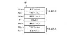
また、図10に示す液晶表示装置1bのように、図8の2軸性フィルム16を、2軸性フィルム16aおよび16bの2枚に分割し、両2軸性フィルム16a・16bを液晶セル11の両側に配してもよい。なお、この場合は、2軸性フィルム16a・16bが特許請求の範囲に記載の第1および第2位相差フィルムに対応する。
【0086】
この場合、2軸性フィルム16aは、面内方向の遅相軸SL16aが、液晶セル11から見て同じ側の偏光板12の吸収軸AA12と直交するように配される。同様に、2軸性フィルム16bの遅相軸SL16bは、液晶セル11から見て同じ側の偏光板13の吸収軸AA13と直交するように配される。この場合であっても、各2軸性フィルム16a・16bの面内方向のリターデーションRxyaおよびRxybを、上記2軸性フィルム16の面内方向のリターデーションRxyの半分に設定し、各2軸性フィルム16a・16bの厚み方向のリターデーションRza・Rzbを、上記2軸性フィルム16の厚み方向のリターデーションRzの半分に設定することによって、同様の効果が得られる。
【0087】
具体的には、TACフィルム12b・13bの厚み方向のリターデーションをRtac〔nm〕、上記面内方向のリターデーションRxyaおよびRxybに関するパラメータα3〔nm〕を、以下の式(9)に示すように、
α3=42.5−0.045×Rlc−Rtac/40 …(9)
とすると、2軸性フィルム16a・16bの面内方向のリターデーションRxya・Rxybは、それぞれ、α3の80%以上かつ120%以下の値に設定されている。
【0088】
また、液晶セル11の厚み方向のリターデーションをRlc〔nm〕、上記リターデーションRza・Rzbに関するパラメータβ3〔nm〕を、以下の式(10)に示すように、
β3=0.525×Rlc−0.95×Rtac …(10)
とすると、2軸性フィルム16a・16bの厚み方向のリターデーションRzaRzbは、それぞれ、β3の60%以上かつ90%以下の値に設定されている。
【0089】
これにより、液晶表示装置1aと同様に、液晶表示装置1bを斜め方向から見た場合のコントラストを10以上と、実用上十分に高い値に保ちながら、上記斜め方向からの観察者が着色および階調つぶれを殆ど感じず、良好な視野角特性を持った液晶表示装置1bを確実に得ることができる。
【0090】
さらに、上記液晶表示装置1aと同様に、上記範囲A1の外周部よりも内部の方が、上記観察者によって把握される着色および階調つぶれが減少するが、特に、図9に示す範囲A2のように、上記リターデーションRxya・Rxybを、それぞれ、上記α3の90%以上かつ110%以下の値に設定すると共に、上記リターデーションRza・Rzbを上記β3の65%以上かつ85%以下に設定することによって、さらに良好な視野角特性を持った液晶表示装置1bを実現できる。
【0091】
したがって、上記着色や階調つぶれの抑制が特に要求される場合には、上記各構成に加えて、上記リターデーションRxyが上記αの90%以上かつ110%以下の値に設定されていると共に、上記リターデーションRzが上記βの65%以上かつ85%以下の値に設定されている方が望ましい。この結果、斜め方向から見た場合の着色や階調つぶれがさらに抑制された液晶表示装置を得ることができる。
【0092】
なお、上記液晶表示装置1aと同様に、当該領域A2内では、上記着色および階調つぶれの改善効果が上記観察者によって認識されず、上記着色および階調つぶれの改善効果が実質上飽和している。したがって、当該領域A2内に設定することによって、同程度の良好な表示品位を有する液晶表示装置1bを実現できる。また、上記リターデーションRxya・Rxybを上記α3と同一に設定し、上記リターデーションRza・Rzbを上記β3と同一に設定すると、斜め方向から見た場合のコントラストが最大になる。さらに、上記リターデーションRxya・Rxybを上記α3の80%〜120%に設定し、上記リターデーションRza・Rzbを上記β3の85%〜90%に設定すれば、着色や階調つぶれを許容範囲内に抑え、しかも、上記領域A2に比較してコントラストを向上できる。
【0093】
〔実施例2〕
本実施例では、上述の実施例1と同様の液晶セル11とTACフィルム12b・13bとを用意し、両者の組み合わせのそれぞれについて、実施例1と同じ斜め方向から見た場合のコントラストが最大となるRxyおよびRzを求めた。これにより、図11に示す実験結果が得られた。
【0094】
図8に示すように、液晶セル11と偏光板12・13の一方(図の場合は、偏光板12)との間に2軸性フィルム16を配した積層順序では、2軸性フィルム16の面内方向のリターデーションRxyが上述のパラメータα2と同一であり、2軸性フィルム16の厚み方向のリターデーションRzが上述のパラメータβ2と同一の場合に、最大のコントラストの液晶表示装置1aが得られることを確認できた。また、上記実験結果を一次式で近似することによって、上述の式(7)および(8)が算出できた。
【0095】
さらに、上記で用意した液晶セル11の場合、上記で用意したような一般的なTACフィルム12b・13b(Rtac=30、50、80〔nm〕)であれば、面内方向のリターデーションRxyの最適値は、45〜65〔nm〕であり、リターデーションRtacは、厚み方向のリターデーションであるにも拘わらず、2軸性フィルム16の面内方向のリターデーションRxyに影響を及ぼしており、TACフィルム12b・13bの影響を単純には取り扱うことができないことも確認できた。
【0096】
加えて、上記リターデーションRxyおよびRzをそれぞれ5%ずつ変化させながら観察者が各液晶表示装置1aの着色および階調つぶれを上記斜め方向から評価した。特に、観察者は、着色現象の有無として、上記斜め方向において、白が黄色や青みがかった色にシフトする現象の有無を評価し、階調つぶれの有無として、明るい領域の階調がつぶれ映像の表現力が低下する現象の有無を評価した。
【0097】
これによって、液晶セル11の厚み方向のリターデーションRlc、および、TACフィルム12b・13bのリターデーションRtacが、上記値のいずれであっても、上記リターデーションRxyが、上記パラメータα2の80%以上かつ120%以下の値であり、しかも、上記リターデーションRzが、上記パラメータβ2の60%以上かつ90%以下の値であれば、上記斜め方向(極角60度)におけるコントラストが10を超え、実使用上、十分なコントラストを維持していることも確認できた。さらに、上記リターデーションRxyおよびRzが上記範囲に設定されていれば、液晶表示装置1aは、上記斜め方向からの観察者が着色および階調つぶれを殆ど感じず、良好な視野角特性を示すことが確認された。また、上記リターデーションRxyが、パラメータα2の80%より小さいか120%よりも大きい場合、および、上記リターデーションRzが、パラメータβ2の60%より小さいか90%よりも大きい場合は、上記斜め方向からの観察者によって、例えば、白が黄色や青みがかった色にシフトする着色現象、あるいは、明るい領域における階調つぶれによって映像の表現力が低下する現象が明確に確認され、観察者が着色や階調つぶれを許容できないことも確認された。
【0098】
加えて、液晶セル11の厚み方向のリターデーションRlc、および、TACフィルム12b・13bのリターデーションRtacが、上記値のいずれであっても、上記リターデーションRxyが、上記パラメータα2の90%以上かつ110%以下の値であり、しかも、上記リターデーションRzが、上記パラメータβ2の65%以上かつ85%以下の値であれば、上記リターデーションRxyが上記パラメータα2の80%〜90%または110%〜120%、あるいは、上記リターデーションRzが上記パラメータβ2の60%〜65%または85%〜90%の場合に比べて、上記斜め方向からの観察者によって把握される着色および階調つぶれが減少することが確認できた。
【0099】
また、上記リターデーションRxyが、上記パラメータα2の90%以上かつ110%以下の値であり、しかも、上記リターデーションRzが、上記パラメータβ2の65%以上かつ85%以下の値であれば、上記着色および階調つぶれの改善効果が実質上飽和し、上記斜め方向からの観察者は、各リターデーションRxyおよびRzが当該範囲に設定されている複数の液晶表示装置1a同士の間で、着色および階調つぶれの相違を確認できず、同程度の良好な表示品位が得られることを確認できた。
【0100】
なお、上記領域A2におけるリターデーションRxyの中心値は、上記斜め方向からコントラストを最大にする上記リターデーションRxy(=α2)の100%(同一の値)であることが確認できた。一方、上記領域A2におけるリターデーションRzの中心値は、上記斜め方向からコントラストを最大にする上記リターデーションRz(=β2)の75%であり、2軸性フィルム16の厚み方向のリターデーションRzをコントラストの最適値β2よりも小さく設定する方が着色現象や階調つぶれを改善できることも確認できた。
【0101】
また、上記リターデーションRxyを80%〜120%に設定し、上記リターデーションRzを85%〜90%に設定すれば、着色や階調つぶれを許容範囲内に抑え、しかも、上記領域A2に比較してコントラストを向上できることが確認できた。
【0102】
また、図10に示す液晶表示装置1bのように、2軸性フィルム16を2枚に分割した構成についても、上記リターデーションRlcおよびRtacが、上記値のいずれであっても、上記斜め視角(極度60度)において最大コントラストを得るためのリターデーションRxya・Rxyb、Rza・Rzbが、図11の液晶表示装置1aの値の半分であり、上記α2およびβ2に代えて、α3およびβ3を基準にすれば、上記液晶表示装置1aと同様の範囲で同様の効果が得られることを確認した。具体的には、上記リターデーションRxya・Rxybを上記α3の80%〜120%に設定し、上記リターデーションRza・Rzbを上記β3の60%〜90%に設定することで、上記斜め視角(極度60度)から見たときに着色および階調つぶれを許容範囲内に抑えることができることを確認した。また、上記リターデーションRxya・Rxybが上記α3の90%〜110%、かつ、上記リターデーションRza・Rzbが上記β3の65%〜85%の範囲では、上記斜め視角における着色および階調つぶれの改善効果が飽和し、同程度に良好な表示品位の液晶表示装置1bが得られることも確認できた。さらに、上記リターデーションRxya・Rxybが上記α3の80%〜120%、かつ、上記リターデーションRza・Rzbが上記β3の85%〜90%の範囲では、上記斜め視角における着色および階調つぶれを許容範囲内に抑えながらコントラストを向上できることを確認できた。
【0103】
なお、上述の第1および第2の実施形態では、液晶セル11を図2ないし図4のように構成して、画素における液晶分子の配向方向を4つに分割する場合について説明したが、これに限るものではない。例えば、図12および図13に示す構造など、他の構造によって配向方向を4分割しても同様の効果が得られる。
【0104】
具体的には、図12に示す画素電極21aを用いた液晶セルでは、図4に示す突起列23a・23bが省略されており、画素電極21aに四角錐状の突起24が設けられている。なお、当該突起24も、上記突起列23aと同様に、画素電極21a上に、感光性樹脂を塗布し、フォトリソグラフィー工程で加工することによって形成できる。
【0105】
この構成でも、突起24の近傍では、液晶分子が各斜面に垂直になるように配向する。加えて、電圧印加時において、突起24の部分の電界は、突起24の斜面に平行になる方向に傾く。これらの結果、電圧印加時において、液晶分子の配向角度の面内成分は、最も近い斜面の法線方向の面内成分(方向P1、P2、P3またはP4)と等しくなる。したがって、画素領域は、傾斜時の配向方向が互いに異なる、4つのドメインD1〜D4に分割される。この結果、図2ないし図4の構造の液晶セル11と同様の効果が得られる。
【0106】
なお、例えば、40インチのような大型の液晶テレビを形成する場合、各画素のサイズは、1mm四方程度と大きくなり、画素電極21aに1つずつ突起24を設けただけでは、配向規制力が弱まり、配向が不安定になる虞れがある。したがって、この場合のように、配向規制力が不足する場合には、各画素電極21a上に複数の突起24を設ける方が望ましい。
【0107】
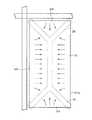
さらに、例えば、図13に示すように、対向基板11bの対向電極21b上にY字状のスリットを上下方向(面内で、略方形状の画素電極21aのいずれかの辺に平行な方向)に対称に連結してなる配向制御窓25を設けても、マルチドメイン配向を実現できる。
【0108】
当該構成では、対向基板11bの表面のうち、配向制御窓25の直下の領域では、電圧を印加しても、液晶分子を傾斜させる程の電界がかからず、液晶分子が垂直に配向する。一方、対向基板11bの表面のうち、配向制御窓25の周囲の領域では、対向基板11bに近づくに従って、配向制御窓25を避けて広がるような電界が発生する。ここで、液晶分子は、長軸が電界に垂直な方向に傾き、液晶分子の配向方向の面内成分は、図中、矢印で示すように、配向制御窓25の各辺に略垂直になる。したがって、この構成であっても、画素における液晶分子の配向方向を4つに分割でき、図2ないし図4の構造の液晶セル11と同様の効果が得られる。
【0109】
また、上記では、配向方向を4分割する場合について説明したが、図14および図15に示すように、放射状配向の液晶セル11を用いても同様の効果が得られる。
【0110】
具体的には、図14に示す構造では、図12に示す突起24に代えて、略半球状の突起26が設けられている。この場合も、突起26の近傍では、液晶分子は、突起26の表面に垂直になるように配向する。加えて、電圧印加時において、突起26の部分の電界は、突起26の表面に平行になる方向に傾く。これらの結果、電圧印加時に液晶分子が傾斜する際、液晶分子は、面内方向で突起26を中心にした放射状に傾きやすくなり、液晶セル11の各液晶分子は、放射状に傾斜配向できる。なお、上記突起26も、上記突起24と同様の工程で形成できる。また、上記突起24と同様に、配向規制力が不足する場合には、各画素電極21a上に複数の突起26を設ける方が望ましい。
【0111】
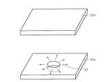
また、図15に示す構造では、図12に示す突起24に代えて、画素電極21aに円形のスリット27が形成されている。これにより、電圧を印加した際、画素電極21aの表面のうち、スリット27の直上の領域では、液晶分子を傾斜させる程の電界がかからない。したがって、この領域では、電圧印加時でも液晶分子は垂直に配向する。一方、画素電極21aの表面のうち、スリット27近傍の領域では、電界は、スリット27へ厚み方向で近づくに従って、スリット27を避けるように傾斜して広がる。ここで、液晶分子は、長軸が垂直な方向に傾き、液晶の連続性によって、スリット27から離れた液晶分子も同様の方向に配向する。したがって、画素電極21aに電圧を印加した場合、各液晶分子は、配向方向の面内成分が、図中、矢印で示すように、スリット27を中心に放射状に広がるように配向、すなわち、スリット27の中心を軸として軸対称に配向できる。ここで、上記電界の傾斜は、印加電圧によって変化するため、液晶分子の配向方向の基板法線方向成分(傾斜角度)は、印加電圧によって制御できる。なお、印加電圧が増加すると、基板法線方向に対する傾斜角が大きくなり、各液晶分子は、表示画面に略平行で、しかも、面内では放射状に配向する。また、上記突起26と同様に、配向規制力が不足する場合には、各画素電極21a上に複数のスリット27を設ける方が望ましい。
【0112】
ところで、上記では、画素における液晶分子の配向方向が分割される場合について説明したが、配向分割しない液晶セル(モノドメインの液晶セル)であっても、略同様の効果が得られる。
【0113】
この場合、画素電極21a・対向電極22bには、突起列23aなどが設けられず、それぞれ平坦に形成されている。さらに、モノドメイン配向の液晶セルの場合、マルチドメイン配向や放射状傾斜配向の液晶セルとは異なり、製造工程にラビング工程が設けられており、液晶層11cの液晶分子のラビング方向が、両基板11a・11bで反平行となるように設定される。また、上記ラビング方向と、偏光板12・13の吸収軸AA12・AA13とが45度の角度になるように、液晶セル11や偏光板12・13が配される。この場合であっても、電圧無印加時には、画素の液晶分子が、図2の場合と同様に、基板法線方向(垂直)に配向している。したがって、上記各実施形態と同様の偏光板12・13、および、位相差板(14〜16、16a・16b)を用いることにより、同様の効果が得られる。
【0114】
ただし、図1および図8に示す液晶表示装置1・1aは、液晶セル11から一方の偏光板12までに配される部材の光学的特性と、液晶セル11から他方の偏光板13までに配される部材の光学的特性とが一致しないので、液晶セル11を左の方位または右の方位から見たときのコントラストと、液晶セル11を上の方位または下の方位から見たときのコントラストとが、互いに異なる虞れがある。したがって、これらの液晶表示装置1・1aにおいて、上下左右の視角特性のバランスを取ることが要求される場合は、4分割配向や放射状配向など、各画素の液晶分子の配向方向が4方向以上に分割される液晶セルを用いる方が望ましい。
【0115】
また、上記では、液晶セル11の液晶層11cが負の誘電異方性を有する場合を例にして説明したが、これに限るものではない。正の誘電異方性を有する場合であっても、図2と同様に、黒表示時に液晶分子が液晶セル11の基板に対して垂直に配向する液晶セルであれば、同様の効果が得られる。
【0116】
この場合は、例えば、IPS(In-Plane Switching)モードで用いる櫛歯電極構造のように、基板平行方向に電界を発生させる電極を用いることによって、液晶層11cに基板平行方向に電界を印加する。この場合であっても、電圧無印加時(無電界時)には、画素の液晶分子は、図2と同様に、基板に対して垂直方向に配向する。したがって、上記各実施形態と同様の偏光板12・13、および、位相差板(14〜16、16a・16b)を用いることで、同様の効果が得られる。
【0117】
【発明の効果】
本発明に係る液晶表示装置は、以上のように、液晶は、負の誘電異方性を有していると共に、両偏光板の一方および液晶セルの間に配され、正の1軸異方性を有する第1位相差フィルムの面内方向のリターデーションをRp〔nm〕、上記偏光板および第1位相差フィルムの間に配され、負の1軸異方性を有する第2位相差フィルムの厚み方向のリターデーションをRn〔nm〕、上記偏光板の基材フィルムの厚み方向のリターデーションをRtac〔nm〕、上記液晶の厚み方向のリターデーションをRlc〔nm〕とし、上記Rpに関するパラメータα〔nm〕を、α=35+(Rlc/80−4)2×3.5+(360−Rlc)×Rtac/850、上記Rnに関するパラメータβ〔nm〕を、β=Rlc−1.9×Rtacとするとき、上記リターデーションRpは、上記αの90%以上かつ110%以下の値に設定されていると共に、上記リターデーションRnは、上記βの65%以上かつ85%以下の値に設定されている構成である。
【0118】
これらの構成によれば、第1および第2位相差フィルムのリターデーションが上述の範囲に設定されているので、基材フィルムの厚み方向のリターデーションを、上記第1および第2位相差フィルムの厚み方向のリターデーションと同等に扱う場合と異なり、斜め方向から見た場合のコントラストが実用上十分に高い値に維持され、しかも、着色や階調つぶれが許容範囲内に抑えられた液晶表示装置を確実に得ることができるという効果を奏する。
【0119】
本発明に係る液晶表示装置は、以上のように、上記構成に加えて、上記液晶の厚み方向のリターデーションRlcは、342〔nm〕から378〔nm〕までの範囲に設定され、上記第1位相差フィルムの面内方向のリターデーションRpが、33.3〔nm〕から38.6〔nm〕までの範囲に設定されている構成である。
【0120】
それゆえ、基材フィルムに製造バラツキが発生して、基材フィルムの厚み方向のリターデーションが変化しても、上記リターデーションRlcおよびRpを上述の範囲に設定することで、当該リターデーションRpを上記αの90%〜110%の範囲に設定できる。この結果、基材フィルムの厚み方向のリターデーションにバラツキが発生する場合であっても、同じ上記第1位相差フィルムを用いることができ、生産性を向上できるという効果を奏する。
【0121】
本発明に係る液晶表示装置は、以上のように、液晶を挟持すると共に当該液晶の液晶分子を表面に概ね垂直に配向させる2枚の基板が設けられた液晶セルと、当該液晶セルの両側に配され、それぞれの吸収軸が互いに直交するように配された2枚の偏光板と、上記両偏光板の一方および上記液晶セルの間に配され、正の1軸異方性を有する第1位相差フィルムと、当該偏光板および第1位相差フィルムの間に配され、負の1軸異方性を有する第2位相差フィルムとを備え、上記液晶は、負の誘電異方性を有していると共に、上記両偏光板には、光軸が上記基板に概ね垂直になるように配置され、負の1軸異方性を有する基材フィルムが設けられ、上記第1位相差フィルムの遅相軸は、上記液晶から見て同じ側の上記偏光板の吸収軸と直交するように配され、上記第2位相差フィルムの光軸が上記基板に概ね垂直になるように配されている液晶表示装置において、上記第1位相差フィルムの面内方向のリターデーションをRp〔nm〕、上記第2位相差フィルムの厚み方向のリターデーションをRn〔nm〕、上記基材フィルムの厚み方向のリターデーションをRtac〔nm〕、上記液晶の厚み方向のリターデーションをRlc〔nm〕とし、上記Rpに関するパラメータα〔nm〕を、α=35+(Rlc/80−4)2×3.5+(360−Rlc)×Rtac/850 上記Rnに関するパラメータβ〔nm〕を、β=Rlc−1.9×Rtacとするとき、上記リターデーションRpは、上記αの80%以上かつ120%以下の値に設定されていると共に、上記リターデーションRnは、上記βの85%以上かつ90%以下の値に設定されている構成である。当該構成によれば、着色や階調つぶれを許容範囲内に抑え、しかも、上記液晶表示装置と比較してコントラストを向上できるという効果を奏する。
【0122】
本発明に係る液晶表示装置は、以上のように、液晶は、負の誘電異方性を有していると共に、両偏光板の一方および上記液晶セルの間に配され、2軸異方性を有する位相差フィルムのリターデーションをRxy〔nm〕、上記位相差フィルムの厚み方向のリターデーションをRz〔nm〕、上記基材フィルムの厚み方向のリターデーションをRtac〔nm〕、上記液晶のあつみ方向のリターデーションをRlc〔nm〕とし、上記Rxyに関するパラメータα〔nm〕を、α=85−0.09×Rlc−Rtac/20、上記Rzに関するパラメータβ〔nm〕を、β=1.05×Rlc−1.9×Rtacとするとき、上記リターデーションRxyは、上記αの90%以上かつ110%以下の値に設定されていると共に、上記リターデーションRzは、上記βの65%以上かつ85%以下の値に設定されている構成である。
【0123】
本発明に係る液晶表示装置は、以上のように、上記液晶は、負の誘電異方性を有していると共に、液晶セルの両側に配され、2軸異方性を有する第1および第2位相差フィルムの面内方向のリターデーションをRxy〔nm〕、厚み方向のリターデーションをRz〔nm〕、上記Rxyに関するパラメータα〔nm〕を、α=42.5−0.045×Rlc−Rtac/40、上記Rzに関するパラメータβ〔nm〕を、β=0.525×Rlc−0.95×Rtacとするとき、上記第1および第2位相差フィルムのリターデーションRxyは、上記αの90%以上かつ110%以下の値に設定されていると共に、上記第1および第2位相差フィルムのリターデーションRzは、上記βの65%以上かつ85%以下の値に設定されている構成である。
【0124】
上記各構成の液晶表示装置では、上記各構成の液晶表示装置では、上記リターデーションRxy、Ryが上述のように設定されているので、基材フィルムの厚み方向のリターデーションを、上記位相差フィルム、あるいは、上記第1および第2位相差フィルムの厚み方向のリターデーションと同等に扱う場合と異なり、斜め方向から見た場合のコントラストが実用上十分に高い値に維持され、しかも、着色や階調つぶれが許容範囲内に抑えられた液晶表示装置を確実に得ることができるという効果を奏する。
【0125】
本発明に係る液晶表示装置は、以上のように、液晶を挟持すると共に当該液晶の液晶分子を表面に概ね垂直に配向させる2枚の基板が設けられた液晶セルと、当該液晶セルの両側に配され、それぞれの吸収軸が互いに直交するように配された2枚の偏光板と、上記両偏光板の一方および上記液晶セルの間に配され、2軸異方性を有する位相差フィルムとを備え、上記液晶は、負の誘電異方性を有していると共に、上記両偏光板には、光軸が上記基板に概ね垂直になるように配置され、負の1軸異方性を有する基材フィルムが設けられ、上記位相差フィルムの面内の遅相軸は、上記液晶から見て同じ側の上記偏光板の吸収軸と直交するように配されている液晶表示装置において、上記位相差フィルムの面内方向のリターデーションをRxy〔nm〕、上記位相差フィルムの厚み方向のリターデーションをRz〔nm〕、上記基材フィルムの厚み方向のリターデーションをRtac〔nm〕、上記液晶の厚み方向のリターデーションをRlc〔nm〕とし、上記Rxyに関するパラメータα〔nm〕を、α=85−0.09×Rlc−Rtac/20 上記Rzに関するパラメータβ〔nm〕を、β=1.05×Rlc−1.9×Rtacとするとき、上記リターデーションRxyは、上記αの80%以上かつ120%以下の値に設定されていると共に、上記リターデーションRzは、上記βの85%以上かつ90%以下の値に設定されている構成である。当該構成によれば、着色や階調つぶれを許容範囲内に抑え、しかも、上記液晶表示装置と比較してコントラストを向上できるという効果を奏する。
【0126】
さらに、本発明に係る液晶表示装置は、以上のように、液晶を挟持すると共に当該液晶の液晶分子を表面に概ね垂直に配向させる2枚の基板が設けられた液晶セルと、当該液晶セルの両側に配され、それぞれの吸収軸が互いに直交するように配された2枚の偏光板と、上記両偏光板の一方および上記液晶セルの間に配され、2軸異方性を有する第1位相差フィルムと、上記両偏光板の他方および上記液晶セルの間に配され、2軸異方性を有する第2位相差フィルムとを備え、上記液晶は、負の誘電異方性を有していると共に、上記両偏光板には、光軸が上記基板に概ね垂直になるように配置され、負の1軸異方性を有する基材フィルムが設けられ、上記第1および第2位相差フィルムの面内の遅相軸は、上記液晶から見て同じ側の上記偏光板の吸収軸と直交するように配されている液晶表示装置において、上記各位相差フィルムの面内方向のリターデーションをRxy〔nm〕、上記各位相差フィルムの厚み方向のリターデーションをRz〔nm〕、上記基材フィルムの厚み方向のリターデーションをRtac〔nm〕、上記液晶の厚み方向のリターデーションをRlc〔nm〕とし、上記Rxyに関するパラメータα〔nm〕を、α=42.5−0.045×Rlc−Rtac/40 上記Rzに関するパラメータβ〔nm〕を、β=0.525×Rlc−0.95×Rtacとするとき、上記第1および第2位相差フィルムのリターデーションRxyは、上記αの80%以上かつ120%以下の値に設定されていると共に、上記第1および第2位相差フィルムのリターデーションRzは、上記βの85%以上かつ90%以下の値に設定されている構成である。当該構成によれば、着色や階調つぶれを許容範囲内に抑え、しかも、上記液晶表示装置と比較してコントラストを向上できるという効果を奏する。
【0127】
本発明に係る液晶表示装置は、以上のように、上記各位相差フィルムが2軸異方性を有するか否かに拘わらず、上記液晶は、負の誘電異方性を有している構成である。
【0128】
当該構成によれば、基板に対して略垂直方向の電界を印加することによって、基板の法線方向に配向した液晶分子を電界強度に応じて傾斜させることができ、正の誘電異方性を有している場合よりも、電極の構造を簡略化できるという効果を奏する。
【図面の簡単な説明】
【図1】 本発明の実施形態を示すものであり、液晶表示装置の要部構成を示す模式図である。
【図2】 上記液晶表示装置に設けられた液晶セルを示すものであり、電圧無印加状態を示す模式図である。
【図3】 上記液晶表示装置に設けられた液晶セルを示すものであり、電圧印加状態を示す模式図である。
【図4】 上記液晶セルの構成例を示すものであり、画素電極近傍を示す平面図である。
【図5】 上記液晶表示装置に設けられた正の1軸性フィルムの面内方向のリターデーションおよび負の1軸性フィルムの厚み方向のリターデーションの好適な範囲を示すものであり、各リターデーションを、それぞれに関するパラメータに対する相対値で示した図面である。
【図6】 本発明の実施例を示すものであり、液晶セルと偏光板との組み合わせについて、上記各リターデーションの最適値の実験結果を示す図面である。
【図7】 液晶表示装置において、コントラストの評価方法を示す図面である。
【図8】 本発明の他の実施形態を示すものであり、液晶表示装置の要部構成を示す模式図である。
【図9】 上記液晶表示装置に設けられた2軸性フィルムの面内方向のリターデーションおよび厚み方向のリターデーションの好適な範囲を示すものであり、各リターデーションを、それぞれに関するパラメータに対する相対値で示した図面である。
【図10】 上記液晶表示装置の変形例を示すものであり、液晶表示装置の要部構成を示す模式図である。
【図11】 本発明の実施例を示すものであり、液晶セルと偏光板との組み合わせについて、上記各リターデーションの最適値の実験結果を示す図面である。
【図12】 上記各液晶表示装置の他の構成例を示すものであり、液晶セルの画素電極を示す斜視図である。
【図13】 上記各液晶表示装置のさらに他の構成例を示すものであり、液晶セルの画素電極近傍を示す平面図である。
【図14】 上記各液晶表示装置の別の構成例を示すものであり、液晶セルの画素電極を示す斜視図である。
【図15】 上記各液晶表示装置のまた別の構成例を示すものであり、液晶セルの画素電極および対向電極を示す斜視図である。
【図16】 従来技術を示すものであり、液晶表示装置の要部構成を示す模式図である。
【図17】 他の従来技術を示すものであり、液晶表示装置の要部構成を示す模式図である。
【符号の説明】
1・1a〜1b 液晶表示装置
11 液晶セル
11a Thin Film Transistor基板(基板)
11b 対向基板(基板)
11c 液晶層(液晶)
12・13 偏光板
12b・13b トリアセチルセルロースフィルム(基材フィルム)
14 正の1軸性フィルム(第1位相差フィルム)
15 負の1軸性フィルム(第2位相差フィルム)
16 2軸性フィルム(位相差フィルム)
16a・16b 2軸性フィルム(第1および第2位相差フィルム)[0001]
BACKGROUND OF THE INVENTION
The present invention relates to a vertical alignment liquid crystal display device.
[0002]
[Prior art]
Conventionally, liquid crystal display devices have been widely used as screens for word processors and computers, and in recent years, they have also rapidly spread as television screens. Many of these liquid crystal display devices employ a TN (Twisted Nematic) mode. However, when viewed from an oblique direction, the liquid crystal display devices tend to have low contrast and inversion of gradation characteristics. There is a problem.
[0003]
Therefore, in recent years, in order to improve the viewing angle characteristics from an oblique direction, a liquid crystal display device in a VA (Verticically Alignment) mode has attracted attention. The liquid crystal cell of the liquid crystal display device in this mode is configured by combining a nematic liquid crystal having negative dielectric anisotropy and a vertical alignment film.
[0004]
Further, for example, in registered patent No. 2947530 and Japanese Patent Laid-Open No. 2000-39610, as shown in FIGS. 16 and 17, in order to optically compensate for the optical anisotropy of the
[0005]
In the above configuration, when the
[0006]
[Problems to be solved by the invention]
However, under the circumstances where a liquid crystal display device with a wider viewing angle and higher display quality is desired today, there is a demand for improvement in coloring and gradation collapse when viewed from an oblique direction. When the retardation films 116 (114 and 115) described in Japanese Patent No. 2947530 and Japanese Patent Application Laid-Open No. 2000-39610 are used, it is not always sufficient, and there is still room for improvement.
[0007]
In view of the above-described problems, the present invention provides a substrate film for a polarizing plate with respect to retardation of each film suitable for suppressing coloring and gradation collapse when viewed from an oblique direction in a liquid crystal display device in a vertical alignment mode. The purpose of this test was to maintain the contrast when viewed from an oblique direction at a sufficiently high value while keeping coloring and gradation loss within a practically acceptable range. It is to provide a liquid crystal display device.
[0008]
[Means for Solving the Problems]
In order to solve the above problems, a liquid crystal display device according to the present invention includes a liquid crystal cell provided with two substrates that sandwich liquid crystal and align liquid crystal molecules of the liquid crystal substantially perpendicularly to the surface, and the liquid crystal cell. The two polarizing plates are arranged on both sides of the polarizing plate so that their absorption axes are orthogonal to each other, between one of the polarizing plates and the liquid crystal cell, and have positive uniaxial anisotropy. A first retardation film having a second retardation film disposed between the polarizing plate and the first retardation film and having negative uniaxial anisotropy,The liquid crystal has negative dielectric anisotropy,Both the polarizing plates are provided with a base film having negative uniaxial anisotropy arranged so that the optical axis is substantially perpendicular to the substrate, and the slow axis of the first retardation film is In the liquid crystal display device, which is disposed so as to be orthogonal to the absorption axis of the polarizing plate on the same side as viewed from the liquid crystal, and is disposed so that the optical axis of the second retardation film is substantially perpendicular to the substrate, It is characterized by the following measures.
[0009]
That is, the retardation in the in-plane direction of the first retardation film is Rp [nm], the retardation in the thickness direction of the second retardation film is Rn [nm], and the retardation in the thickness direction of the base film is Rtac [nm], retardation in the thickness direction of the liquid crystal is Rlc [nm], and the parameter α [nm] related to the Rp is α = 35 + (Rlc / 80-4)2× 3.5 + (360−Rlc) × Rtac / 850, where the parameter β [nm] for Rn is β = Rlc−1.9 × Rtac, the retardation Rp is90% or moreAnd110% or lessAnd the retardation Rn is the value of β.65% or moreAnd85% or lessIs set to the value of
[0010]
In the liquid crystal display device having the above-described configuration, the liquid crystal molecules aligned substantially perpendicular to the substrate do not give a phase difference to the light incident from the normal direction of the substrate. Gives a phase difference according to the polar angle (inclination angle from the normal direction), so that without the first and second retardation films, the light that should be absorbed by the output side polarizing plate is essentially It is not completely absorbed. As a result, light leakage occurs and the contrast is lowered, and coloring and gradation loss occur.
[0011]
On the other hand, in the said structure, since the said 1st and 2nd phase difference film is provided, the phase difference which the said liquid crystal gave according to the polar angle is compensated by both phase difference films. As a result, it is possible to prevent light leakage when viewed from an oblique direction, improve the contrast, and prevent coloring and gradation collapse.
[0012]
However, when determining the retardation of the both retardation films, the thickness direction of the base film from the retardation in the thickness direction of the first and second retardation films, which is optimal when there is no base film. It is not always sufficient to subtract the retardation in a situation where further suppression of coloring and gradation collapse is required when viewed from an oblique direction.
[0013]
Therefore, the inventor of the present application has conducted research to further suppress coloring and gradation collapse while maintaining a contrast sufficiently high in practical use when the liquid crystal display device in the vertical alignment mode is viewed from an oblique direction. As a result, it has been found that the retardation in the thickness direction of the base film does not act in the same way as the retardation in the thickness direction of the first and second retardation films, and in particular positive uniaxial anisotropy. When setting the retardation Rp in the in-plane direction of the first retardation film to have the maximum contrast, depending on whether the retardation of the liquid crystal exceeds 360 [nm], The dependence of the retardation Rp on the retardation in the thickness direction is reversed and the contrast is maximized. Relative to each retardation, by setting the predetermined range, it found that collapse can be effectively suppressed coloration and gradation, thereby completing the present invention.
[0014]
In the liquid crystal display device of the present invention, in accordance with the substrate film and retardation Rtac and Rlc in the thickness direction of the liquid crystal, while maintaining the contrast when viewed from an oblique direction at a sufficiently high practical value, The retardations Rp and Rn are set in a range where gradation collapse can be allowed. Thereby, unlike the case where the retardation in the thickness direction of the base film is handled in the same way as the retardation in the thickness direction of the first and second retardation films, the contrast when viewed from the oblique direction is sufficiently practical. It is possible to reliably obtain a liquid crystal display device that is maintained at a high value and in which coloring and gradation deterioration are suppressed within an allowable range.
[0015]
In addition, in the case where both the suppression of coloring and gradation collapse and the improvement of productivity are particularly required, in addition to the above configuration, the retardation Rlc in the thickness direction of the liquid crystal is from 342 [nm] to 378. It is desirable that the retardation Rp in the in-plane direction of the first retardation film is set in the range from 33.3 [nm] to 38.6 [nm]. .
[0016]
If the retardations Rlc and Rp are set within the above range, even if production variation occurs in the base film and the retardation in the thickness direction of the base film changes, the retardation Rp is changed to the above α. It can be set in the range of 90% to 110%. As a result, even if the retardation in the thickness direction of the base film varies, the same first retardation film can be used, and productivity can be improved.
[0017]
The liquid crystal display device according to the present invention is disposed on both sides of the liquid crystal cell provided with two substrates for sandwiching the liquid crystal and aligning the liquid crystal molecules of the liquid crystal substantially perpendicularly to the surface, Two polarizing plates arranged such that their absorption axes are orthogonal to each other, and a first retardation film arranged between one of the polarizing plates and the liquid crystal cell and having positive uniaxial anisotropy And a second retardation film disposed between the polarizing plate and the first retardation film and having negative uniaxial anisotropy, wherein the liquid crystal has negative dielectric anisotropy. In addition, both the polarizing plates are provided with a base film having a negative uniaxial anisotropy arranged so that an optical axis is substantially perpendicular to the substrate, and a slow axis of the first retardation film. Is arranged so as to be orthogonal to the absorption axis of the polarizing plate on the same side as viewed from the liquid crystal. In the liquid crystal display device in which the optical axis of the second retardation film is arranged so as to be substantially perpendicular to the substrate, the retardation in the in-plane direction of the first retardation film is Rp [nm], The retardation in the thickness direction of the second retardation film is Rn [nm], the retardation in the thickness direction of the substrate film is Rtac [nm], the retardation in the thickness direction of the liquid crystal is Rlc [nm], and the above Rp Parameter α [nm] with respect to α = 35 + (Rlc / 80-4)2× 3.5 + (360−Rlc) × Rtac / 850 When the parameter β [nm] for Rn is β = Rlc−1.9 × Rtac, the retardation Rp is 80% or more of the α and 120 The retardation Rn is set to a value of 85% or more and 90% or less of the β. According to this configuration, it is possible to suppress coloring and gradation loss within an allowable range, and to improve contrast as compared with the liquid crystal display device.
[0018]
On the other hand, in order to solve the above problems, a liquid crystal display device according to the present invention includes a liquid crystal cell provided with two substrates for sandwiching liquid crystal and aligning liquid crystal molecules of the liquid crystal substantially perpendicularly to the surface; Two polarizing plates arranged on both sides of the liquid crystal cell, the absorption axes of which are arranged so as to be orthogonal to each other, and between one of the polarizing plates and the liquid crystal cell. A retardation film havingThe liquid crystal has negative dielectric anisotropy,Both polarizing plates are provided with a base film having negative uniaxial anisotropy arranged so that the optical axis is substantially perpendicular to the substrate, and the in-plane slow axis of the retardation film is In the liquid crystal display device arranged so as to be orthogonal to the absorption axis of the polarizing plate on the same side as viewed from the liquid crystal, the following measures are taken.
[0019]
That is, the retardation in the in-plane direction of the retardation film is Rxy [nm], the retardation in the thickness direction of the retardation film is Rz [nm], and the retardation in the thickness direction of the base film is Rtac [nm]. The retardation of the liquid crystal in the assembling direction is Rlc [nm], the parameter α [nm] for Rxy is α = 85−0.09 × Rlc−Rtac / 20, and the parameter β [nm] for Rz is When β = 1.05 × Rlc−1.9 × Rtac, the retardation Rxy is90% or moreAnd110% or lessAnd the retardation Rz is the value of β.65% or moreAnd85% or lessIs set to the value of
[0020]
In order to solve the above problems, a liquid crystal display device according to the present invention includes a liquid crystal cell provided with two substrates for sandwiching liquid crystal and aligning liquid crystal molecules of the liquid crystal substantially perpendicularly to the surface; Two polarizing plates arranged on both sides of the liquid crystal cell, the absorption axes of which are arranged so as to be orthogonal to each other, and between one of the polarizing plates and the liquid crystal cell. A first retardation film having a second retardation film disposed between the other of the polarizing plates and the liquid crystal cell and having biaxial anisotropy,The liquid crystal has negative dielectric anisotropy,Both the polarizing plates are provided with a base film having a negative uniaxial anisotropy arranged so that an optical axis is substantially perpendicular to the substrate, and in-plane with the first and second retardation films. In the liquid crystal display device in which the slow axis is arranged so as to be orthogonal to the absorption axis of the polarizing plate on the same side as viewed from the liquid crystal, the following measures are taken.
[0021]
That is, the retardation in the in-plane direction of each retardation film is Rxy [nm], the retardation in the thickness direction of each retardation film is Rz [nm], and the retardation in the thickness direction of the base film is Rtac [nm]. The retardation in the thickness direction of the liquid crystal is Rlc [nm], the parameter α [nm] related to the Rxy is α = 42.5−0.045 × Rlc−Rtac / 40, the parameter β [nm] related to the Rz Is β = 0.525 × Rlc−0.95 × Rtac, the retardation Rxy of the first and second retardation films is90% or moreAnd110% or lessThe retardation Rz of the first and second retardation films is set to the value of β.65% or moreAnd85% or lessIs set to the value of
[0022]
In the liquid crystal display device having each configuration described above, the phase difference given to the light in the oblique direction by the liquid crystal in the state where the liquid crystal molecules are aligned substantially perpendicular to the substrate is the retardation film or the first and second positions. Compensated by the phase difference film, prevents light leakage when viewed from an oblique direction, and improves contrast.
[0023]
However, even if it is the said structure, when determining the retardation of the said retardation film or the 1st and 2nd retardation film, from the retardation of the thickness direction which each retardation film has optimal when there is no base film In addition, it is not always sufficient to subtract the retardation in the thickness direction of the substrate film in a situation where further suppression of coloring and gradation collapse is required when viewed from an oblique direction. .
[0024]
Therefore, the present inventor has conducted research to further improve the contrast when the vertical alignment mode liquid crystal display device is viewed from an oblique direction, and as a result, as in the above-described liquid crystal display device, the thickness direction of the base film It has been found that the retardation does not act in the same manner as the retardation in the thickness direction of the retardation film or the first and second retardation films. Further, the retardation Rxy in the in-plane direction having biaxial anisotropy and the retardation Rtac in the thickness direction of the base film are the retardation Rxy, although the retardation directions are different from each other. In order to set appropriately, the influence of the retardation Rtac should be taken into account, and by setting the predetermined range based on each of the above retardations that maximizes the contrast, the coloration and gradation collapse Has been found to be effectively suppressed, and the present invention has been completed.
[0025]
In the liquid crystal display device of the present invention, when setting the retardation Rxy in the in-plane direction and the retardation Rz in the thickness direction of the retardation film or the first and second retardation films, The retardation Rxy is set in accordance with the retardations Rlc and Rtac in the thickness direction, and the retardation Rxy is within a range in which coloring and gradation collapse can be allowed while maintaining a contrast sufficiently high when viewed from an oblique direction. And Rz are set. Thereby, the retardation in the thickness direction of the base film is different from the case of handling the retardation film or the retardation in the thickness direction of the first and second retardation films, as viewed from the oblique direction. Is maintained at a sufficiently high value for practical use, and a liquid crystal display device in which coloring and gradation collapse are suppressed within an allowable range can be reliably obtained.
[0026]
The liquid crystal display device according to the present invention is disposed on both sides of the liquid crystal cell provided with two substrates for sandwiching the liquid crystal and aligning the liquid crystal molecules of the liquid crystal substantially perpendicularly to the surface, Two polarizing plates arranged so that the respective absorption axes are orthogonal to each other, a retardation film arranged between one of the polarizing plates and the liquid crystal cell, and having biaxial anisotropy, The liquid crystal has negative dielectric anisotropy, and the both polarizing plates are arranged so that the optical axis is substantially perpendicular to the substrate, and has a negative uniaxial anisotropy. In the liquid crystal display device, in which the film is provided, and the in-plane slow axis of the retardation film is arranged to be orthogonal to the absorption axis of the polarizing plate on the same side as viewed from the liquid crystal, the retardation film The retardation in the in-plane direction is Rxy [nm], above The retardation in the thickness direction of the retardation film is Rz [nm], the retardation in the thickness direction of the substrate film is Rtac [nm], the retardation in the thickness direction of the liquid crystal is Rlc [nm], and the parameters related to Rxy α = 85−0.09 × Rlc−Rtac / 20 When the parameter β [nm] related to Rz is β = 1.05 × Rlc−1.9 × Rtac, the retardation Rxy Is set to a value between 80% and 120% of α, and the retardation Rz is set to a value between 85% and 90% of β. According to this configuration, it is possible to suppress coloring and gradation loss within an allowable range, and to improve contrast as compared with the liquid crystal display device.
[0027]
Furthermore, the liquid crystal display device according to the present invention is disposed on both sides of the liquid crystal cell provided with two substrates for sandwiching the liquid crystal and aligning the liquid crystal molecules of the liquid crystal substantially perpendicular to the surface, Two polarizing plates arranged so that their respective absorption axes are orthogonal to each other, a first retardation film having a biaxial anisotropy disposed between one of the polarizing plates and the liquid crystal cell, A second retardation film having a biaxial anisotropy disposed between the other of the polarizing plates and the liquid crystal cell, wherein the liquid crystal has a negative dielectric anisotropy, and Both polarizing plates are provided with a base film having a negative uniaxial anisotropy arranged so that the optical axis is substantially perpendicular to the substrate, and within the planes of the first and second retardation films. The slow axis is orthogonal to the absorption axis of the polarizing plate on the same side as seen from the liquid crystal In the liquid crystal display device arranged as described above, the retardation in the in-plane direction of each retardation film is Rxy [nm], the retardation in the thickness direction of each retardation film is Rz [nm], The retardation in the thickness direction is Rtac [nm], the retardation in the thickness direction of the liquid crystal is Rlc [nm], and the parameter α [nm] related to the Rxy is α = 42.5−0.045 × Rlc−Rtac / 40 When the parameter β [nm] related to Rz is β = 0.525 × Rlc−0.95 × Rtac, the retardation Rxy of the first and second retardation films is 80% or more of α and The retardation Rz of the first and second retardation films is set to a value of 120% or less, and the β is 85. It is characterized in that it is set above and to the value of 90% or less. According to this configuration, it is possible to suppress coloring and gradation loss within an allowable range, and to improve contrast as compared with the liquid crystal display device.
[0028]
Furthermore, in the liquid crystal display device according to the present invention, the liquid crystal has negative dielectric anisotropy regardless of whether or not each of the retardation films has biaxial anisotropy.So, the baseBy applying an electric field in a direction substantially perpendicular to the plate, the liquid crystal molecules aligned in the normal direction of the substrate can be tilted according to the electric field strength, compared with the case where it has positive dielectric anisotropy. However, the structure of the electrode can be simplified.
[0029]
DETAILED DESCRIPTION OF THE INVENTION
[First Embodiment]
An embodiment of the present invention will be described below with reference to FIGS. As will be described in detail later, the present invention can be applied to other liquid crystal cells. Hereinafter, a multi-domain aligned liquid crystal cell will be described as a preferred example.
[0030]
As shown in FIG. 1, the liquid
[0031]
As shown in FIG. 2, the
[0032]
Further, a
[0033]
Here, the
[0034]
Specifically, as shown in FIG. 4, the
[0035]
Here, in the vicinity of the
[0036]
As a result, in each of the
[0037]
Here, each protrusion row | line |
[0038]
On the other hand, the polarizing plates 12 and 13 shown in FIG. 1 include
[0039]
Further, the positive
Rp = dp · (nxp−nyp) (1)
Is calculated by Further, the positive
[0040]
On the other hand, the negative
Rn = dn · {(nxn + nyn) / 2−nzn} (2)
Is calculated by Further, the negative
[0041]
In the liquid
[0042]
Here, the absorption axes AA12 and AA13 of the polarizing plates 12 and 13 are arranged so as to be orthogonal to each other. As described in detail later, the positive
[0043]
Accordingly, the light incident on the polarizing plate (for example, 12) on the emission side becomes elliptically polarized light corresponding to the phase difference given by the
[0044]
Further, in the
[0045]
On the other hand, while no voltage is applied between the
[0046]
Here, the light incident on the
[0047]
However, in the configuration shown in FIG. 1, since the positive
[0048]
Here, in the liquid
[0049]
Specifically, the retardation in the thickness direction of the
α1 = 35 + (Rlc / 80-4)2× 3.5
+ (360−Rlc) × Rtac / 850 (3)
Then, the retardation Rp in the in-plane direction of the positive
[0050]
Further, the retardation in the thickness direction of the
β1 = Rlc−1.9 × Rtac (4)
Then, the retardation Rn in the thickness direction of the negative
[0051]
Thus, by setting the retardations Rp and Rn within the range A1 shown in FIG. 5 with the parameters α1 and β1 as a reference, the contrast when the liquid
[0052]
Further, although the coloring and gradation crushing grasped by the observer is reduced in the inside than in the outer peripheral portion of the range A1, in particular, the retardation Rp is set as described above in the range A2 shown in FIG. By setting the value of α1 to 90% to 110% and setting the retardation Rn to 65% to 85% of β1, the liquid
[0053]
In the area A2, the effect of improving the coloring and gradation loss is not recognized by the observer, and the effect of improving the coloring and gradation deterioration is substantially saturated. Therefore, the liquid
[0054]
Here, as apparent from the above formula (3), the optimum value of the retardation Rp in the in-plane direction of the positive
[0055]
Accordingly, by setting the retardation Rlc in the thickness direction of the
[0056]
Further, when the retardation Rlc is in the range of 324 [nm] to 396 [nm] and the retardation Rp is in the range of 30.7 [nm] to 41.7 [nm], the retardation Rtac is If it is a general value, ie, about 30 [nm] to 80 [nm], the retardation Rp falls within the range of 80% to 120% of α1. As a result, by setting the retardation Rn to 60% to 90% of β1, the contrast when the liquid
[0057]
Therefore, when importance is placed on improvement in productivity, the retardation Rlc in the thickness direction of the
[0058]
Thereby, even when the retardation Rtac fluctuates due to manufacturing variations of the
[0059]
Thus, in the case where improvement in productivity is particularly required, the above-described configuration, that is, a liquid crystal cell provided with two substrates that sandwich the liquid crystal and align liquid crystal molecules of the liquid crystal substantially perpendicularly to the surface And two polarizing plates arranged on both sides of the liquid crystal cell and arranged such that their absorption axes are orthogonal to each other, and between one of the polarizing plates and the liquid crystal cell, a positive 1 A first retardation film having axial anisotropy; and a second retardation film disposed between the polarizing plate and the first retardation film and having negative uniaxial anisotropy. Is provided with a base film having a negative uniaxial anisotropy arranged so that the optical axis is substantially perpendicular to the substrate, and the slow axis of the first retardation film is viewed from the liquid crystal. Arranged to be orthogonal to the absorption axis of the polarizing plate on the same side, In the liquid crystal display device in which the optical axis of the two retardation film is arranged substantially perpendicular to the substrate, the retardation in the in-plane direction of the first retardation film is Rp [nm], and the second retardation is The retardation in the thickness direction of the film is Rn [nm], the retardation in the thickness direction of the base film is Rtac [nm], the retardation in the thickness direction of the liquid crystal is Rlc [nm], and the parameter α [ nm], α = 35 + (Rlc / 80-4)2× 3.5 + (360−Rlc) × Rtac / 850, where the parameter β [nm] related to Rn is β = Rlc−1.9 × Rtac, the retardation Rp is 80% or more of α and The retardation Rn is set to a value of 120% or less, and the retardation Rn is set to a value of 60% or more and 90% or less of β. The retardation Rp in the in-plane direction of the first retardation film is set in the range from 30.7 [nm] to 41.7 [nm]. It is desirable that it is set.
[0060]
If the retardation Rlc is set within the range, the retardation Rp has little dependency on the retardation in the thickness direction of the base film. Therefore, even if manufacturing variation occurs in the base film and the retardation in the thickness direction of the base film changes, the retardation Rp is set to the above α by setting the retardation Rp to the above range. It can be set in the range of 80% to 120%. As a result, even if the retardation in the thickness direction of the base film varies, the same first retardation film can be used, and productivity can be improved.
[0061]
Furthermore, in the case where suppression of the coloring and gradation collapse is particularly required, in addition to the above-described configuration, the retardation Rp is set to a value of 90% to 110% of α, and It is desirable that the retardation Rn is set to a value not less than 65% and not more than 85% of β. Thereby, it is possible to obtain a liquid crystal display device in which coloring and gradation collapse when viewed from an oblique direction are further suppressed.
[0062]
Further, when both improvement in productivity and better viewing angle characteristics are emphasized, the retardation Rlc is set in the range of 342 [nm] to 378 [nm], and the retardation Rp is 33. It is desirable to set in the range of 3 [nm] to 38.6 [nm]. In this case, if the retardation Rtac is a general value, that is, about 30 [nm] to 80 [nm], the retardation Rp falls within the range of 90% to 110% of α1. Therefore, by setting the retardation Rn to 65% to 85% of β1, the liquid
[0063]
[Example 1]
In this embodiment, as the
[0064]
When measuring the contrast, the viewing angle when the liquid
[0065]
Thereby, as shown in FIG. 1, the in-plane direction of the positive
[0066]
Further, in the case of the
[0067]
Further, by setting the retardation Rlc in the thickness direction of the
[0068]
In addition, the observer evaluated the coloration and gradation collapse of each liquid
[0069]
Thereby, even if the retardation Rlc in the thickness direction of the
[0070]
In addition, even if the retardation Rlc in the thickness direction of the
[0071]
When the retardation Rp is 90% or more and 110% or less of the parameter α1, and the retardation Rn is 65% or more and 85% or less of the parameter β1, The improvement effect of coloring and gradation collapse is substantially saturated, and an observer from the above oblique direction can perform coloring and coloring between the plurality of liquid
[0072]
It has been confirmed that the center value of the retardation Rp in the region A2 is 100% (the same value) of the retardation Rp (= α1) that maximizes the contrast from the oblique direction. On the other hand, the center value of the retardation Rn in the region A2 is 75% of the retardation Rn (= β1) that maximizes the contrast from the oblique direction, and the retardation of the negative
[0073]
Moreover, if the retardation Rp is set to 80% to 120% of the α1 and the retardation Rn is set to 85% to 90% of the β1, the coloring and gradation collapse are suppressed within an allowable range, and It has been confirmed that the contrast can be improved as compared with the region A2.
[0074]
Further, the retardation Rlc of the
[0075]
[Second Embodiment]
The liquid crystal display device 1a according to the present embodiment is similar to the configuration of the liquid
[0076]
The
Rxy = d2 · (nx2-ny2) (5)
Rz = d2 · {(nx2 + ny2) / 2−nz2} (6)
Is calculated by The
[0077]
Even in this case, when the
[0078]
Furthermore, in the liquid crystal display device 1a according to the present embodiment, in order to obtain a liquid crystal display device that exhibits good color and good gradation characteristics while maintaining a sufficiently high contrast for practical use as an oblique viewing angle display quality. More specifically, in order to prevent the observer from the above direction from almost seeing coloration and gradation collapse while keeping the contrast when viewed from an oblique direction at 10 or more, a sufficiently high value for practical use. The retardation of the
[0079]
Specifically, the retardation in the thickness direction of the
α2 = 85−0.09 × Rlc−Rtac / 20 (7)
Then, the retardation Rxy in the in-plane direction of the
[0080]
Further, the retardation in the thickness direction of the
β2 = 1.05 × Rlc−1.9 × Rtac (8)
Then, the retardation Rz in the thickness direction of the
[0081]
Thus, by setting the retardations Rxy and Rz within the range A1 shown in FIG. 9 with the parameters α2 and β2 as a reference, the contrast when the liquid crystal display device 1a is viewed from an oblique direction is 10 or more. Thus, while maintaining a practically high value, the observer from the oblique direction hardly feels coloring and gradation collapse, and the liquid crystal display device 1a having good viewing angle characteristics can be reliably obtained.
[0082]
Further, although coloring and gradation collapse that are grasped by the observer are reduced in the inside than in the outer peripheral portion of the range A1, the retardation Rxy is set to the retardation Rxy, particularly in the range A2 shown in FIG. By setting the value of α2 to 90% or more and 110% or less, and setting the retardation Rz to 65% or more and 85% or less of β2, the liquid crystal display device 1a having a better viewing angle characteristic. Can be realized.
[0083]
Therefore, in the case where suppression of the coloring and gradation collapse is particularly required, the retardation Rxy is set to a value of 90% or more and 110% or less of the α in addition to the above-described components, It is desirable that the retardation Rz is set to a value not less than 65% and not more than 85% of the β. As a result, it is possible to obtain a liquid crystal display device in which coloring and gradation collapse when viewed from an oblique direction are further suppressed.
[0084]
In the area A2, the effect of improving the coloring and gradation loss is not recognized by the observer, and the effect of improving the coloring and gradation deterioration is substantially saturated. Therefore, the liquid crystal display device 1a having the same good display quality can be realized by setting the area A2. Further, when the retardation Rxy is set to be the same as α2, and the retardation Rz is set to be the same as β2, the contrast when viewed from an oblique direction is maximized. Furthermore, if the retardation Rxy is set to 80% to 120% of the α2 and the retardation Rz is set to 85% to 90% of the β2, the coloring and gradation collapse are suppressed within an allowable range. The contrast can be improved as compared with the region A2.
[0085]
Further, like the liquid
[0086]
In this case, the biaxial film 16a is arranged so that the slow axis SL16a in the in-plane direction is orthogonal to the absorption axis AA12 of the polarizing plate 12 on the same side when viewed from the
[0087]
Specifically, the retardation in the thickness direction of the
α3 = 42.5−0.045 × Rlc−Rtac / 40 (9)
Then, the retardations Rxya and Rxyb in the in-plane direction of the
[0088]
Further, the retardation in the thickness direction of the
β3 = 0.525 × Rlc−0.95 × Rtac (10)
Then, the retardation RzaRzb in the thickness direction of the
[0089]
Thus, similarly to the liquid crystal display device 1a, the observer from the oblique direction can change the color and level while keeping the contrast when the liquid
[0090]
Further, like the liquid crystal display device 1a, the coloring and gradation collapse that are grasped by the observer are reduced more in the inside than in the outer peripheral portion of the range A1, but in particular, in the range A2 shown in FIG. Thus, the retardations Rxya and Rxyb are set to values of 90% or more and 110% or less of the α3, respectively, and the retardations Rza and Rzb are set to 65% or more and 85% or less of the β3. As a result, the liquid
[0091]
Therefore, in the case where suppression of the coloring and gradation collapse is particularly required, the retardation Rxy is set to a value of 90% or more and 110% or less of the α in addition to the above-described components, It is desirable that the retardation Rz is set to a value not less than 65% and not more than 85% of the β. As a result, it is possible to obtain a liquid crystal display device in which coloring and gradation collapse when viewed from an oblique direction are further suppressed.
[0092]
As in the liquid crystal display device 1a, in the region A2, the effect of improving the coloring and gradation loss is not recognized by the observer, and the effect of improving the coloring and gradation deterioration is substantially saturated. Yes. Therefore, the liquid
[0093]
[Example 2]
In this example, the same
[0094]
As shown in FIG. 8, in the stacking order in which the
[0095]
Furthermore, in the case of the
[0096]
In addition, the observer evaluated the coloring and gradation collapse of each liquid crystal display device 1a from the oblique direction while changing the retardations Rxy and Rz by 5% respectively. In particular, the observer evaluates the presence or absence of a coloring phenomenon and the presence or absence of a phenomenon in which white shifts to a yellowish or bluish color in the diagonal direction. The presence or absence of a phenomenon in which expressive power was reduced was evaluated.
[0097]
Thereby, the retardation Rxy in the thickness direction of the
[0098]
In addition, even if the retardation Rlc in the thickness direction of the
[0099]
If the retardation Rxy is a value of 90% to 110% of the parameter α2, and the retardation Rz is a value of 65% to 85% of the parameter β2, The improvement effect of coloring and gradation collapse is substantially saturated, and the observer from the oblique direction can perform coloring and coloring between the plurality of liquid crystal display devices 1a in which the retardations Rxy and Rz are set in the range. The difference in gradation collapse could not be confirmed, and it was confirmed that the same good display quality was obtained.
[0100]
It has been confirmed that the center value of the retardation Rxy in the region A2 is 100% (the same value) of the retardation Rxy (= α2) that maximizes the contrast from the oblique direction. On the other hand, the center value of the retardation Rz in the region A2 is 75% of the retardation Rz (= β2) that maximizes the contrast from the oblique direction, and the retardation Rz in the thickness direction of the
[0101]
Further, if the retardation Rxy is set to 80% to 120% and the retardation Rz is set to 85% to 90%, coloring and gradation collapse are suppressed within an allowable range, and compared with the region A2. It was confirmed that the contrast could be improved.
[0102]
Further, even in the configuration in which the
[0103]
In the first and second embodiments described above, the
[0104]
Specifically, in the liquid crystal cell using the
[0105]
Even in this configuration, the liquid crystal molecules are aligned so as to be perpendicular to the inclined surfaces in the vicinity of the
[0106]
For example, when forming a large-sized liquid crystal television such as 40 inches, the size of each pixel is as large as about 1 mm square, and the alignment regulating force can be obtained only by providing one
[0107]
Further, for example, as shown in FIG. 13, a Y-shaped slit is formed in the vertical direction on the
[0108]
In this configuration, in the region immediately below the
[0109]
Further, in the above description, the case where the alignment direction is divided into four has been described. However, as shown in FIGS. 14 and 15, the same effect can be obtained even when the radially aligned
[0110]
Specifically, in the structure shown in FIG. 14, a substantially
[0111]
In the structure shown in FIG. 15, a
[0112]
By the way, although the case where the alignment direction of the liquid crystal molecules in a pixel is divided | segmented above was demonstrated, the substantially same effect is acquired even if it is a liquid crystal cell (monodomain liquid crystal cell) which is not alignment-divided.
[0113]
In this case, the
[0114]
However, in the liquid
[0115]
In the above description, the case where the
[0116]
In this case, an electric field is applied in the substrate parallel direction to the
[0117]
【The invention's effect】
The liquid crystal display device according to the present invention is as described above.The liquid crystal has negative dielectric anisotropy andThe retardation in the in-plane direction of the first retardation film that is arranged between one of the polarizing plates and the liquid crystal cell and has positive uniaxial anisotropy is Rp [nm], and the polarizing plate and the first retardation film. The retardation in the thickness direction of the second retardation film having negative uniaxial anisotropy is Rn [nm], and the retardation in the thickness direction of the base film of the polarizing plate is Rtac [nm]. The retardation in the thickness direction of the liquid crystal is Rlc [nm], and the parameter α [nm] for the Rp is α = 35 + (Rlc / 80-4).2× 3.5 + (360−Rlc) × Rtac / 850, where the parameter β [nm] for Rn is β = Rlc−1.9 × Rtac, the retardation Rp is90% or moreAnd110% or lessAnd the retardation Rn is the value of β.65% or moreAnd85% or lessThe configuration is set to the value of.
[0118]
According to these configurations, since the retardation of the first and second retardation films is set in the above-described range, the retardation in the thickness direction of the base film is set to be the same as that of the first and second retardation films. Unlike the case where it is handled in the same way as the retardation in the thickness direction, a liquid crystal display device in which the contrast when viewed from an oblique direction is maintained at a sufficiently high value for practical use, and coloring and gradation collapse are suppressed within an allowable range. Has the effect of reliably obtaining.
[0119]
BookAs described above, in the liquid crystal display device according to the invention, in addition to the above configuration, the retardation Rlc in the thickness direction of the liquid crystal is set in a range from 342 [nm] to 378 [nm], and the first place The retardation Rp in the in-plane direction of the retardation film is set in a range from 33.3 [nm] to 38.6 [nm].
[0120]
Therefore, even if manufacturing variations occur in the base film and the retardation in the thickness direction of the base film changes, the retardation Rp is set by setting the retardations Rlc and Rp in the above-mentioned range. It can be set in the range of 90% to 110% of α. As a result, even if the retardation in the thickness direction of the base film varies, the same first retardation film can be used, and the productivity can be improved.
[0121]
As described above, the liquid crystal display device according to the present invention includes a liquid crystal cell provided with two substrates for sandwiching liquid crystal and aligning liquid crystal molecules of the liquid crystal substantially perpendicularly to the surface, and both sides of the liquid crystal cell. A first polarizing plate having a positive uniaxial anisotropy, disposed between one of the two polarizing plates and the liquid crystal cell. A retardation film and a second retardation film disposed between the polarizing plate and the first retardation film and having negative uniaxial anisotropy, wherein the liquid crystal has negative dielectric anisotropy. In addition, each of the polarizing plates is provided with a base film having a negative uniaxial anisotropy arranged so that an optical axis is substantially perpendicular to the substrate, and the first retardation film of the first retardation film. The slow axis is orthogonal to the absorption axis of the polarizing plate on the same side as seen from the liquid crystal. In the liquid crystal display device in which the optical axis of the second retardation film is arranged so as to be substantially perpendicular to the substrate, the retardation in the in-plane direction of the first retardation film is Rp [nm]. The retardation in the thickness direction of the second retardation film is Rn [nm], the retardation in the thickness direction of the base film is Rtac [nm], the retardation in the thickness direction of the liquid crystal is Rlc [nm], The parameter α [nm] related to Rp is set to α = 35 + (Rlc / 80−4)2× 3.5 + (360−Rlc) × Rtac / 850 When the parameter β [nm] for Rn is β = Rlc−1.9 × Rtac, the retardation Rp is 80% or more of the α and 120 %, And the retardation Rn is set to a value not less than 85% and not more than 90% of the β. According to this configuration, it is possible to suppress the coloring and gradation loss within an allowable range, and to improve the contrast as compared with the liquid crystal display device.
[0122]
The liquid crystal display device according to the present invention is as described above.The liquid crystal has negative dielectric anisotropy andThe retardation of the retardation film having biaxial anisotropy disposed between one of the polarizing plates and the liquid crystal cell is Rxy [nm], the retardation in the thickness direction of the retardation film is Rz [nm], The retardation in the thickness direction of the base film is Rtac [nm], the retardation in the assembling direction of the liquid crystal is Rlc [nm], and the parameter α [nm] related to the Rxy is α = 85−0.09 × Rlc. -Rtac / 20, where β = 1.05 × Rlc−1.9 × Rtac is a parameter β [nm] related to Rz, the retardation Rxy is90% or moreAnd110% or lessAnd the retardation Rz is the value of β.65% or moreAnd85% or lessThe configuration is set to the value of.
[0123]
The liquid crystal display device according to the present invention is as described above.The liquid crystal has negative dielectric anisotropy,The retardation in the in-plane direction of the first and second retardation films having biaxial anisotropy disposed on both sides of the liquid crystal cell is Rxy [nm], the retardation in the thickness direction is Rz [nm], and the above Rxy When the parameter α [nm] is α = 42.5−0.045 × Rlc−Rtac / 40, and the parameter β [nm] related to the Rz is β = 0.525 × Rlc−0.95 × Rtac, The retardation Rxy of the first and second retardation films is α90% or moreAnd110% or lessThe retardation Rz of the first and second retardation films is set to the value of β.65% or moreAnd85% or lessThe configuration is set to the value of.
[0124]
In the liquid crystal display device of each configuration described above, in the liquid crystal display device of each configuration described above, since the retardations Rxy and Ry are set as described above, the retardation in the thickness direction of the base film is changed to the retardation film. Or, unlike the case where the first and second retardation films are handled in the same manner as the retardation in the thickness direction, the contrast when viewed from the oblique direction is maintained at a sufficiently high value for practical use, and the There is an effect that it is possible to reliably obtain a liquid crystal display device in which the adjustment is suppressed within an allowable range.
[0125]
As described above, the liquid crystal display device according to the present invention sandwiches the liquid crystal and the liquid crystal component of the liquid crystal.A liquid crystal cell provided with two substrates for orienting the element substantially perpendicular to the surface, and two polarizing plates arranged on both sides of the liquid crystal cell and having their respective absorption axes orthogonal to each other; A retardation film having a biaxial anisotropy disposed between one of the polarizing plates and the liquid crystal cell, the liquid crystal having negative dielectric anisotropy, The plate is provided with a base film having a negative uniaxial anisotropy arranged so that the optical axis is substantially perpendicular to the substrate, and the slow axis in the plane of the retardation film is the liquid crystal In the liquid crystal display device arranged to be orthogonal to the absorption axis of the polarizing plate on the same side as viewed from the above, the retardation in the in-plane direction of the retardation film is Rxy [nm], the thickness direction of the retardation film The retardation of Rz [nm] The retardation in the thickness direction of the rum is Rtac [nm], the retardation in the thickness direction of the liquid crystal is Rlc [nm], and the parameter α [nm] related to the Rxy is α = 85−0.09 × Rlc−Rtac / 20 When the parameter β [nm] related to Rz is β = 1.05 × Rlc−1.9 × Rtac, the retardation Rxy is set to a value of 80% or more and 120% or less of the α. In addition, the retardation Rz is set to a value of 85% or more and 90% or less of the β. According to this configuration, it is possible to suppress the coloring and gradation loss within an allowable range, and to improve the contrast as compared with the liquid crystal display device.
[0126]
Furthermore, the liquid crystal display device according to the present invention includes, as described above, a liquid crystal cell provided with two substrates for sandwiching liquid crystal and aligning liquid crystal molecules of the liquid crystal substantially perpendicularly to the surface; Two polarizing plates arranged on both sides and arranged such that their absorption axes are orthogonal to each other, and a first biaxial anisotropy arranged between one of the polarizing plates and the liquid crystal cell A retardation film, and a second retardation film disposed between the other of the polarizing plates and the liquid crystal cell and having biaxial anisotropy, and the liquid crystal has negative dielectric anisotropy. In addition, both the polarizing plates are provided with a base film having a negative uniaxial anisotropy disposed so that an optical axis is substantially perpendicular to the substrate, and the first and second retardations are provided. The slow axis in the plane of the film is the polarizing plate on the same side as seen from the liquid crystal In the liquid crystal display device arranged to be orthogonal to the absorption axis, the retardation in the in-plane direction of each retardation film is Rxy [nm], the retardation in the thickness direction of each retardation film is Rz [nm], The retardation in the thickness direction of the base film is Rtac [nm], the retardation in the thickness direction of the liquid crystal is Rlc [nm], and the parameter α [nm] related to the Rxy is α = 42.5−0.045 × Rlc−Rtac / 40 When the parameter β [nm] related to Rz is β = 0.525 × Rlc−0.95 × Rtac, the retardation Rxy of the first and second retardation films is The retardation Rz of the first and second retardation films is set to a value of 80% or more and 120% or less. The β is set to a value of 85% or more and 90% or less. According to this configuration, it is possible to suppress the coloring and gradation loss within an allowable range, and to improve the contrast as compared with the liquid crystal display device.
[0127]
As described above, the liquid crystal display device according to the present invention has a configuration in which the liquid crystal has negative dielectric anisotropy regardless of whether each of the retardation films has biaxial anisotropy. is there.
[0128]
According to this configuration, by applying an electric field in a direction substantially perpendicular to the substrate, liquid crystal molecules aligned in the normal direction of the substrate can be tilted according to the electric field strength, and positive dielectric anisotropy can be achieved. There is an effect that the structure of the electrode can be simplified as compared with the case of having it.
[Brief description of the drawings]
FIG. 1, showing an embodiment of the present invention, is a schematic diagram showing a configuration of a main part of a liquid crystal display device.
FIG. 2 shows a liquid crystal cell provided in the liquid crystal display device, and is a schematic diagram showing a state in which no voltage is applied.
FIG. 3 shows a liquid crystal cell provided in the liquid crystal display device, and is a schematic diagram showing a voltage application state.
FIG. 4 is a plan view showing a configuration example of the liquid crystal cell and showing the vicinity of a pixel electrode.
FIG. 5 shows preferred ranges of in-plane retardation of a positive uniaxial film and retardation in a thickness direction of a negative uniaxial film provided in the liquid crystal display device. It is drawing which showed the foundation by the relative value with respect to the parameter regarding each.
FIG. 6 shows an example of the present invention, and is a diagram showing experimental results of optimum values of the above-mentioned respective retardations for a combination of a liquid crystal cell and a polarizing plate.
FIG. 7 is a drawing showing a contrast evaluation method in a liquid crystal display device.
FIG. 8, showing another embodiment of the present invention, is a schematic diagram showing a configuration of a main part of a liquid crystal display device.
FIG. 9 shows a preferable range of retardation in the in-plane direction and retardation in the thickness direction of the biaxial film provided in the liquid crystal display device, and each retardation is a relative value with respect to a parameter relating to each. It is drawing shown by.
FIG. 10 shows a modification of the liquid crystal display device, and is a schematic diagram showing a main configuration of the liquid crystal display device.
FIG. 11 shows an example of the present invention, and is a drawing showing experimental results of optimum values of the above-mentioned respective retardations for a combination of a liquid crystal cell and a polarizing plate.
FIG. 12 is a perspective view showing a pixel electrode of a liquid crystal cell, showing another configuration example of each liquid crystal display device.
FIG. 13 is a plan view showing the vicinity of a pixel electrode of a liquid crystal cell, showing still another configuration example of each of the liquid crystal display devices.
FIG. 14 is a perspective view showing a pixel electrode of a liquid crystal cell, showing another configuration example of each liquid crystal display device.
FIG. 15 is a perspective view showing a pixel electrode and a counter electrode of a liquid crystal cell, showing still another configuration example of each of the liquid crystal display devices.
FIG. 16 is a schematic diagram illustrating a configuration of a main part of a liquid crystal display device according to a related art.
FIG. 17 is a schematic diagram showing a configuration of a main part of a liquid crystal display device, showing another conventional technique.
[Explanation of symbols]
1.1a to 1b liquid crystal display device
11 Liquid crystal cell
11a Thin Film Transistor substrate (substrate)
11b Counter substrate (substrate)
11c Liquid crystal layer (liquid crystal)
12.13 Polarizing plate
12b / 13b Triacetylcellulose film (base film)
14 Positive uniaxial film (first retardation film)
15 Negative uniaxial film (second retardation film)
16 Biaxial film (retardation film)
16a and 16b biaxial films (first and second retardation films)
Claims (7)
Translated fromJapanese上記液晶は、負の誘電異方性を有していると共に、
上記両偏光板には、光軸が上記基板に概ね垂直になるように配置され、負の1軸異方性を有する基材フィルムが設けられ、上記第1位相差フィルムの遅相軸は、上記液晶から見て同じ側の上記偏光板の吸収軸と直交するように配され、上記第2位相差フィルムの光軸が上記基板に概ね垂直になるように配されている液晶表示装置のリターデーションの設定方法において、
上記第1位相差フィルムの面内方向のリターデーションをRp〔nm〕、上記第2位相差フィルムの厚み方向のリターデーションをRn〔nm〕、上記基材フィルムの厚み方向のリターデーションをRtac〔nm〕、上記液晶の厚み方向のリターデーションをRlc〔nm〕とし、
上記Rpに関するパラメータα〔nm〕を、
α=35+(Rlc/80−4)2×3.5
+(360−Rlc)×Rtac/850
上記Rnに関するパラメータβ〔nm〕を、
β=Rlc−1.9×Rtac
とするとき、
上記リターデーションRpを、上記αの90%以上かつ110%以下の値に設定すると共に、上記リターデーションRnを、上記βの65%以上かつ85%以下の値に設定することを特徴とする液晶表示装置のリターデーションの設定方法。A liquid crystal cell provided with two substrates for sandwiching the liquid crystal and aligning the liquid crystal molecules of the liquid crystal substantially perpendicularly to the surface, and arranged on both sides of the liquid crystal cell so that the respective absorption axes are orthogonal to each other. Two polarizing plates, a first retardation film having a positive uniaxial anisotropy disposed between one of the polarizing plates and the liquid crystal cell, and the polarizing plate and the first retardation film A second retardation film disposed between and having negative uniaxial anisotropy,
The liquid crystal has negative dielectric anisotropy,
Both polarizing plates are provided with a base film having a negative uniaxial anisotropy arranged so that the optical axis is substantially perpendicular to the substrate, and the slow axis of the first retardation film is:A litter for a liquid crystal display device, which is arranged so as to be orthogonal to the absorption axis of the polarizing plate on the same side as viewed from the liquid crystal, and arranged so that the optical axis of the second retardation film is substantially perpendicular to the substrateIn the setting method of thefoundation ,
The retardation in the in-plane direction of the first retardation film is Rp [nm], the retardation in the thickness direction of the second retardation film is Rn [nm], and the retardation in the thickness direction of the base film is Rtac [ nm], the retardation in the thickness direction of the liquid crystal is Rlc [nm],
The parameter α [nm] for Rp is
α = 35 + (Rlc / 80-4)2 × 3.5
+ (360-Rlc) × Rtac / 850
The parameter β [nm] for Rn is
β = Rlc−1.9 × Rtac
And when
Liquid crystalthe retardation Rp, together with theset of 90% or more and 110% or less of the value of the alpha,the retardation Rn, andsets 65% or more and the following values 85% of the βSetting method of retardation of display device.
上記液晶は、負の誘電異方性を有していると共に、
上記両偏光板には、光軸が上記基板に概ね垂直になるように配置され、負の1軸異方性を有する基材フィルムが設けられ、上記第1位相差フィルムの遅相軸は、上記液晶から見て同じ側の上記偏光板の吸収軸と直交するように配され、上記第2位相差フィルムの光軸が上記基板に概ね垂直になるように配されている液晶表示装置のリターデーションの設定方法において、
上記第1位相差フィルムの面内方向のリターデーションをRp〔nm〕、上記第2位相差フィルムの厚み方向のリターデーションをRn〔nm〕、上記基材フィルムの厚み方向のリターデーションをRtac〔nm〕、上記液晶の厚み方向のリターデーションをRlc〔nm〕とし、
上記Rpに関するパラメータα〔nm〕を、
α=35+(Rlc/80−4)2×3.5
+(360−Rlc)×Rtac/850
上記Rnに関するパラメータβ〔nm〕を、
β=Rlc−1.9×Rtac
とするとき、
上記リターデーションRpを、上記αの80%以上かつ120%以下の値に設定すると共に、上記リターデーションRnを、上記βの85%以上かつ90%以下の値に設定することを特徴とする液晶表示装置のリターデーションの設定方法。A liquid crystal cell provided with two substrates for sandwiching the liquid crystal and aligning the liquid crystal molecules of the liquid crystal substantially perpendicularly to the surface, and arranged on both sides of the liquid crystal cell so that the respective absorption axes are orthogonal to each other. Two polarizing plates, a first retardation film having a positive uniaxial anisotropy disposed between one of the polarizing plates and the liquid crystal cell, and the polarizing plate and the first retardation film A second retardation film disposed between and having negative uniaxial anisotropy,
The liquid crystal has negative dielectric anisotropy,
Both polarizing plates are provided with a base film having a negative uniaxial anisotropy arranged so that the optical axis is substantially perpendicular to the substrate, and the slow axis of the first retardation film is:A litter for a liquid crystal display device, which is arranged so as to be orthogonal to the absorption axis of the polarizing plate on the same side as viewed from the liquid crystal, and arranged so that the optical axis of the second retardation film is substantially perpendicular to the substrateIn the setting method of thefoundation ,
The retardation in the in-plane direction of the first retardation film is Rp [nm], the retardation in the thickness direction of the second retardation film is Rn [nm], and the retardation in the thickness direction of the base film is Rtac [ nm], the retardation in the thickness direction of the liquid crystal is Rlc [nm],
The parameter α [nm] for Rp is
α = 35 + (Rlc / 80-4)2 × 3.5
+ (360-Rlc) × Rtac / 850
The parameter β [nm] for Rn is
β = Rlc−1.9 × Rtac
And when
Liquid crystalthe retardation Rp,while set at 80% or more and 120% or less of the value of the alpha,the retardation Rn, andsets 85% or more and 90% or less of the value of the βSetting method of retardation of display device.
上記液晶は、負の誘電異方性を有していると共に、
上記両偏光板には、光軸が上記基板に概ね垂直になるように配置され、負の1軸異方性を有する基材フィルムが設けられ、上記位相差フィルムの面内の遅相軸は、上記液晶から見て同じ側の上記偏光板の吸収軸と直交するように配されている液晶表示装置のリターデーションの設定方法において、
上記位相差フィルムの面内方向のリターデーションをRxy〔nm〕、上記位相差フィルムの厚み方向のリターデーションをRz〔nm〕、上記基材フィルムの厚み方向のリターデーションをRtac〔nm〕、上記液晶の厚み方向のリターデーションをRlc〔nm〕とし、
上記Rxyに関するパラメータα〔nm〕を、
α=85−0.09×Rlc−Rtac/20
上記Rzに関するパラメータβ〔nm〕を、
β=1.05×Rlc−1.9×Rtac
とするとき、
上記リターデーションRxyを、上記αの90%以上かつ110%以下の値に設定すると共に、上記リターデーションRzを、上記βの65%以上かつ85%以下の値に設定することを特徴とする液晶表示装置のリターデーションの設定方法。A liquid crystal cell provided with two substrates for sandwiching the liquid crystal and aligning the liquid crystal molecules of the liquid crystal substantially perpendicularly to the surface, and arranged on both sides of the liquid crystal cell so that the respective absorption axes are orthogonal to each other. The two polarizing plates, and a retardation film disposed between one of the polarizing plates and the liquid crystal cell and having biaxial anisotropy,
The liquid crystal has negative dielectric anisotropy,
Both polarizing plates are provided with a base film having negative uniaxial anisotropy arranged so that the optical axis is substantially perpendicular to the substrate, and the in-plane slow axis of the retardation film is In themethod of setting the retardation of the liquid crystal display device arranged to be orthogonal to the absorption axis of the polarizing plate on the same side as viewed from the liquid crystal,
The retardation in the in-plane direction of the retardation film is Rxy [nm], the retardation in the thickness direction of the retardation film is Rz [nm], the retardation in the thickness direction of the base film is Rtac [nm], and The retardation in the thickness direction of the liquid crystal is Rlc [nm],
The parameter α [nm] related to Rxy is
α = 85−0.09 × Rlc−Rtac / 20
The parameter β [nm] related to Rz is
β = 1.05 × Rlc−1.9 × Rtac
And when
Liquid crystalthe retardation Rxy,while set at 90% or more and 110% or less of the value of the alpha,the retardation Rz, andsets 65% or more and the following values 85% of the βSetting method of retardation of display device.
上記液晶は、負の誘電異方性を有していると共に、
上記両偏光板には、光軸が上記基板に概ね垂直になるように配置され、負の1軸異方性を有する基材フィルムが設けられ、上記位相差フィルムの面内の遅相軸は、上記液晶から見て同じ側の上記偏光板の吸収軸と直交するように配されている液晶表示装置のリターデーションの設定方法において、
上記位相差フィルムの面内方向のリターデーションをRxy〔nm〕、上記位相差フィルムの厚み方向のリターデーションをRz〔nm〕、上記基材フィルムの厚み方向のリターデーションをRtac〔nm〕、上記液晶の厚み方向のリターデーションをRlc〔nm〕とし、
上記Rxyに関するパラメータα〔nm〕を、
α=85−0.09×Rlc−Rtac/20
上記Rzに関するパラメータβ〔nm〕を、
β=1.05×Rlc−1.9×Rtac
とするとき、
上記リターデーションRxyを、上記αの80%以上かつ120%以下の値に設定すると共に、上記リターデーションRzを、上記βの85%以上かつ90%以下の値に設定することを特徴とする液晶表示装置のリターデーションの設定方法。A liquid crystal cell provided with two substrates for sandwiching the liquid crystal and aligning the liquid crystal molecules of the liquid crystal substantially perpendicularly to the surface, and arranged on both sides of the liquid crystal cell so that the respective absorption axes are orthogonal to each other. The two polarizing plates, and a retardation film disposed between one of the polarizing plates and the liquid crystal cell and having biaxial anisotropy,
The liquid crystal has negative dielectric anisotropy,
Both polarizing plates are provided with a base film having negative uniaxial anisotropy arranged so that the optical axis is substantially perpendicular to the substrate, and the in-plane slow axis of the retardation film is In themethod of setting the retardation of the liquid crystal display device arranged to be orthogonal to the absorption axis of the polarizing plate on the same side as viewed from the liquid crystal,
The retardation in the in-plane direction of the retardation film is Rxy [nm], the retardation in the thickness direction of the retardation film is Rz [nm], the retardation in the thickness direction of the base film is Rtac [nm], and The retardation in the thickness direction of the liquid crystal is Rlc [nm],
The parameter α [nm] related to Rxy is
α = 85−0.09 × Rlc−Rtac / 20
The parameter β [nm] related to Rz is
β = 1.05 × Rlc−1.9 × Rtac
And when
Liquid crystalthe retardation Rxy,while set at 80% or more and 120% or less of the value of the alpha,the retardation Rz, andsets 85% or more and 90% or less of the value of the βSetting method of retardation of display device.
上記液晶は、負の誘電異方性を有していると共に、
上記両偏光板には、光軸が上記基板に概ね垂直になるように配置され、負の1軸異方性を有する基材フィルムが設けられ、上記第1および第2位相差フィルムの面内の遅相軸は、上記液晶から見て同じ側の上記偏光板の吸収軸と直交するように配されている液晶表示装置のリターデーションの設定方法において、
上記各位相差フィルムの面内方向のリターデーションをRxy〔nm〕、上記各位相差フィルムの厚み方向のリターデーションをRz〔nm〕、上記基材フィルムの厚み方向のリターデーションをRtac〔nm〕、上記液晶の厚み方向のリターデーションをRlc〔nm〕とし、
上記Rxyに関するパラメータα〔nm〕を、
α=42.5−0.045×Rlc−Rtac/40
上記Rzに関するパラメータβ〔nm〕を、
β=0.525×Rlc−0.95×Rtac
とするとき、
上記第1および第2位相差フィルムのリターデーションRxyを、上記αの90%以上かつ110%以下の値に設定すると共に、上記第1および第2位相差フィルムのリターデーションRzを、上記βの65%以上かつ85%以下の値に設定することを特徴とする液晶表示装置のリターデーションの設定方法。A liquid crystal cell provided with two substrates for sandwiching the liquid crystal and aligning the liquid crystal molecules of the liquid crystal substantially perpendicularly to the surface, and arranged on both sides of the liquid crystal cell so that the respective absorption axes are orthogonal to each other. Two polarizing plates, a first retardation film having biaxial anisotropy disposed between one of the polarizing plates and the liquid crystal cell, and the other of the polarizing plates and the liquid crystal cell. A second retardation film disposed between and having biaxial anisotropy,
The liquid crystal has negative dielectric anisotropy,
Both the polarizing plates are provided with a base film having a negative uniaxial anisotropy arranged so that an optical axis is substantially perpendicular to the substrate, and in-plane with the first and second retardation films. In themethod of setting the retardation of the liquid crystal display device, the slow axis is arranged so as to be orthogonal to the absorption axis of the polarizing plate on the same side as viewed from the liquid crystal,
The retardation in the in-plane direction of each retardation film is Rxy [nm], the retardation in the thickness direction of each retardation film is Rz [nm], the retardation in the thickness direction of the base film is Rtac [nm], The retardation in the thickness direction of the liquid crystal is Rlc [nm],
The parameter α [nm] related to Rxy is
α = 42.5−0.045 × Rlc−Rtac / 40
The parameter β [nm] related to Rz is
β = 0.525 × Rlc−0.95 × Rtac
And when
The retardation Rxyof the first and second retardation films is setto a value of 90% or more and 110% or less of the α, and the retardation Rzof the first and second retardation films is setto the βsetting the retardation of the liquid crystal display device andsetting the following values less than 65% and 85%.
上記液晶は、負の誘電異方性を有していると共に、
上記両偏光板には、光軸が上記基板に概ね垂直になるように配置され、負の1軸異方性を有する基材フィルムが設けられ、上記第1および第2位相差フィルムの面内の遅相軸は、上記液晶から見て同じ側の上記偏光板の吸収軸と直交するように配されている液晶表示装置のリターデーションの設定方法において、
上記各位相差フィルムの面内方向のリターデーションをRxy〔nm〕、上記各位相差フィルムの厚み方向のリターデーションをRz〔nm〕、上記基材フィルムの厚み方向のリターデーションをRtac〔nm〕、上記液晶の厚み方向のリターデーションをRlc〔nm〕とし、
上記Rxyに関するパラメータα〔nm〕を、
α=42.5−0.045×Rlc−Rtac/40
上記Rzに関するパラメータβ〔nm〕を、
β=0.525×Rlc−0.95×Rtac
とするとき、
上記第1および第2位相差フィルムのリターデーションRxyを、上記αの80%以上かつ120%以下の値に設定すると共に、上記第1および第2位相差フィルムのリターデーションRzを、上記βの85%以上かつ90%以下の値に設定することを特徴とする液晶表示装置のリターデーションの設定方法。A liquid crystal cell provided with two substrates for sandwiching the liquid crystal and aligning the liquid crystal molecules of the liquid crystal substantially perpendicularly to the surface, and arranged on both sides of the liquid crystal cell so that the respective absorption axes are orthogonal to each other. Two polarizing plates, a first retardation film having biaxial anisotropy disposed between one of the polarizing plates and the liquid crystal cell, and the other of the polarizing plates and the liquid crystal cell. A second retardation film disposed between and having biaxial anisotropy,
The liquid crystal has negative dielectric anisotropy,
Both the polarizing plates are provided with a base film having a negative uniaxial anisotropy arranged so that an optical axis is substantially perpendicular to the substrate, and in-plane with the first and second retardation films. In themethod of setting the retardation of the liquid crystal display device, the slow axis is arranged so as to be orthogonal to the absorption axis of the polarizing plate on the same side as viewed from the liquid crystal,
The retardation in the in-plane direction of each retardation film is Rxy [nm], the retardation in the thickness direction of each retardation film is Rz [nm], the retardation in the thickness direction of the base film is Rtac [nm], The retardation in the thickness direction of the liquid crystal is Rlc [nm],
The parameter α [nm] related to Rxy is
α = 42.5−0.045 × Rlc−Rtac / 40
The parameter β [nm] related to Rz is
β = 0.525 × Rlc−0.95 × Rtac
And when
The retardation Rxyof the first and second retardation films is setto a value not less than 80% and not more than 120% of the α, and the retardation Rzof the first and second retardation films is setto the β Aretardation setting method for a liquid crystal display device, characterizedin that the value is setto 85% or more and 90% or less.
Priority Applications (8)
| Application Number | Priority Date | Filing Date | Title |
|---|---|---|---|
| JP2002064481AJP3993000B2 (en) | 2002-03-08 | 2002-03-08 | Setting method of retardation of liquid crystal display device |
| CNB038055686ACN100368896C (en) | 2002-03-08 | 2003-03-04 | Liquid crystal display device |
| US10/467,765US6885421B2 (en) | 2002-03-08 | 2003-03-04 | Liquid crystal display device |
| AU2003211481AAU2003211481A1 (en) | 2002-03-08 | 2003-03-04 | Liquid crystal display unit |
| PCT/JP2003/002521WO2003077020A1 (en) | 2002-03-08 | 2003-03-04 | Liquid crystal display unit |
| KR1020047014036AKR100697744B1 (en) | 2002-03-08 | 2003-03-04 | Liquid crystal display |
| TW092104801ATWI230826B (en) | 2002-03-08 | 2003-03-06 | Liquid crystal display device |
| US11/090,798US7095467B2 (en) | 2002-03-08 | 2005-03-25 | Liquid crystal display device |
Applications Claiming Priority (1)
| Application Number | Priority Date | Filing Date | Title |
|---|---|---|---|
| JP2002064481AJP3993000B2 (en) | 2002-03-08 | 2002-03-08 | Setting method of retardation of liquid crystal display device |
Related Child Applications (1)
| Application Number | Title | Priority Date | Filing Date |
|---|---|---|---|
| JP2005158180ADivisionJP2005266829A (en) | 2005-05-30 | 2005-05-30 | Liquid crystal display |
Publications (2)
| Publication Number | Publication Date |
|---|---|
| JP2003262872A JP2003262872A (en) | 2003-09-19 |
| JP3993000B2true JP3993000B2 (en) | 2007-10-17 |
Family
ID=27800219
Family Applications (1)
| Application Number | Title | Priority Date | Filing Date |
|---|---|---|---|
| JP2002064481AExpired - Fee RelatedJP3993000B2 (en) | 2002-03-08 | 2002-03-08 | Setting method of retardation of liquid crystal display device |
Country Status (7)
| Country | Link |
|---|---|
| US (2) | US6885421B2 (en) |
| JP (1) | JP3993000B2 (en) |
| KR (1) | KR100697744B1 (en) |
| CN (1) | CN100368896C (en) |
| AU (1) | AU2003211481A1 (en) |
| TW (1) | TWI230826B (en) |
| WO (1) | WO2003077020A1 (en) |
Families Citing this family (34)
| Publication number | Priority date | Publication date | Assignee | Title |
|---|---|---|---|---|
| US7401923B2 (en)* | 2004-03-09 | 2008-07-22 | Fergason Patent Properties, Llc | Monitor for showing high-resolution and three-dimensional images and method |
| US20060268407A1 (en)* | 2000-07-07 | 2006-11-30 | Fergason James L | Display system using two displays and polarization direction rotation for showing high-resolution and three-dimensional images and method and use of a DBEF beam splitter |
| JP4329983B2 (en)* | 2003-02-05 | 2009-09-09 | 大日本印刷株式会社 | Liquid crystal display |
| US7508474B2 (en)* | 2003-04-07 | 2009-03-24 | Dai Nippon Printing Co., Ltd. | Laminated retardation layer, its fabrication process, and liquid crystal display incorporating the same |
| TWI242083B (en)* | 2003-08-11 | 2005-10-21 | Sony Corp | Liquid crystal display device |
| JP4883518B2 (en)* | 2003-12-12 | 2012-02-22 | Nltテクノロジー株式会社 | Liquid crystal display |
| JP2005201960A (en)* | 2004-01-13 | 2005-07-28 | Seiko Epson Corp | Liquid crystal device and projection display device |
| JP4904665B2 (en)* | 2004-02-25 | 2012-03-28 | コニカミノルタオプト株式会社 | Liquid crystal display and polarizing plate set |
| JP4255893B2 (en)* | 2004-07-16 | 2009-04-15 | 富士通株式会社 | Liquid crystal display |
| CN100397186C (en)* | 2004-09-16 | 2008-06-25 | 东芝松下显示技术有限公司 | Liquid crystal display element |
| US7450204B1 (en) | 2004-11-02 | 2008-11-11 | University Of Central Florida Research Foundation, Inc. | Multi-film compensated liquid crystal display with initial homogeneous alignment |
| KR100682230B1 (en)* | 2004-11-12 | 2007-02-12 | 주식회사 엘지화학 | Vertically Aligned Liquid Crystal Display |
| JP4536489B2 (en)* | 2004-11-15 | 2010-09-01 | 株式会社 日立ディスプレイズ | Optical element and display device using the same |
| WO2006060236A2 (en)* | 2004-11-23 | 2006-06-08 | Fergason Patent Properties, Llc | Monitor for showing high-resolution and three-dimensional images |
| US7411636B2 (en) | 2004-11-23 | 2008-08-12 | Fergason Patent Properties, Llc | Stereoscopic liquid crystal display (LCD) with polarization method |
| JP2007163894A (en)* | 2005-12-14 | 2007-06-28 | Fujifilm Corp | Liquid crystal display |
| JP4301327B2 (en)* | 2006-08-24 | 2009-07-22 | セイコーエプソン株式会社 | Projector with optical device |
| US7532288B2 (en)* | 2007-01-26 | 2009-05-12 | Casio Computer Co., Ltd. | Liquid crystal display device |
| JP4311492B2 (en)* | 2007-01-26 | 2009-08-12 | カシオ計算機株式会社 | Liquid crystal display element and broadcast receiving apparatus |
| JP5228559B2 (en)* | 2008-03-25 | 2013-07-03 | ソニー株式会社 | Image display device and optical compensation device |
| JP2009289592A (en)* | 2008-05-29 | 2009-12-10 | Canon Inc | Display |
| JP5292020B2 (en)* | 2008-08-28 | 2013-09-18 | スタンレー電気株式会社 | Liquid crystal display element |
| JP2010085696A (en)* | 2008-09-30 | 2010-04-15 | Fujifilm Corp | Liquid crystal display device |
| US8749740B2 (en)* | 2009-09-08 | 2014-06-10 | Sharp Kabushiki Kaisha | Liquid crystal display device |
| JP5727131B2 (en)* | 2009-09-24 | 2015-06-03 | スタンレー電気株式会社 | Liquid crystal display element |
| JP2011164209A (en)* | 2010-02-05 | 2011-08-25 | Casio Computer Co Ltd | Liquid crystal display element |
| JP5632625B2 (en)* | 2010-03-04 | 2014-11-26 | 富士フイルム株式会社 | VA liquid crystal display device |
| US9164308B2 (en)* | 2012-08-22 | 2015-10-20 | Shenzhen China Star Optoelectronics Technology Co., Ltd. | Optical compensation structure and display device |
| CN102798922B (en)* | 2012-08-22 | 2014-12-03 | 深圳市华星光电技术有限公司 | Optical compensation structure and display device |
| US9011993B2 (en)* | 2012-08-23 | 2015-04-21 | Shenzhen China Star Optoelectronics Technology Co., Ltd. | Optical compensation structure and display device |
| CN102854654B (en)* | 2012-09-11 | 2015-09-02 | 深圳市华星光电技术有限公司 | Display device |
| CN102854661B (en)* | 2012-10-10 | 2015-06-03 | 深圳市华星光电技术有限公司 | VA display mode compensating framework and VA display mode liquid crystal display device |
| CN103869538A (en)* | 2014-04-04 | 2014-06-18 | 深圳市华星光电技术有限公司 | Compensation framework of liquid crystal panel and liquid crystal display device |
| JP6805877B2 (en)* | 2017-02-22 | 2020-12-23 | 住友ゴム工業株式会社 | Rubber composition for tires and pneumatic tires |
Family Cites Families (12)
| Publication number | Priority date | Publication date | Assignee | Title |
|---|---|---|---|---|
| DE4308003A1 (en) | 1993-03-13 | 1994-09-15 | Fleissner Maschf Gmbh Co | Double winding device |
| JPH10153802A (en)* | 1996-09-30 | 1998-06-09 | Fujitsu Ltd | Liquid crystal display |
| US6642981B1 (en)* | 1996-09-30 | 2003-11-04 | Fujitsu Display Technologies Corporation | Liquid crystal display device operating in a vertically aligned mode including at least one retardation film |
| TW509808B (en) | 1997-06-12 | 2002-11-11 | Sharp Kk | Liquid crystal display device |
| JP3526533B2 (en)* | 1997-08-29 | 2004-05-17 | シャープ株式会社 | Liquid crystal display device and television device |
| EP2098906A1 (en) | 1997-08-29 | 2009-09-09 | Sharp Kabushiki Kaisha | Liquid crystal display device |
| JP2000019518A (en)* | 1997-09-25 | 2000-01-21 | Sharp Corp | Liquid crystal display |
| JP3470567B2 (en) | 1997-09-25 | 2003-11-25 | 住友化学工業株式会社 | Liquid crystal display and viewing angle compensation film used therefor |
| JP3299190B2 (en)* | 1998-07-15 | 2002-07-08 | インターナショナル・ビジネス・マシーンズ・コーポレーション | Liquid crystal display |
| JP3926072B2 (en)* | 1998-12-18 | 2007-06-06 | シャープ株式会社 | Liquid crystal display |
| US6359671B1 (en)* | 2000-02-23 | 2002-03-19 | Planar Systems, Inc. | High contrast liquid crystal device |
| JP3863446B2 (en)* | 2002-03-08 | 2006-12-27 | シャープ株式会社 | Liquid crystal display |
- 2002
- 2002-03-08JPJP2002064481Apatent/JP3993000B2/ennot_activeExpired - Fee Related
- 2003
- 2003-03-04KRKR1020047014036Apatent/KR100697744B1/ennot_activeExpired - Fee Related
- 2003-03-04WOPCT/JP2003/002521patent/WO2003077020A1/enactiveApplication Filing
- 2003-03-04USUS10/467,765patent/US6885421B2/ennot_activeExpired - Lifetime
- 2003-03-04CNCNB038055686Apatent/CN100368896C/ennot_activeExpired - Fee Related
- 2003-03-04AUAU2003211481Apatent/AU2003211481A1/ennot_activeAbandoned
- 2003-03-06TWTW092104801Apatent/TWI230826B/ennot_activeIP Right Cessation
- 2005
- 2005-03-25USUS11/090,798patent/US7095467B2/ennot_activeExpired - Fee Related
Also Published As
| Publication number | Publication date |
|---|---|
| CN1639621A (en) | 2005-07-13 |
| TWI230826B (en) | 2005-04-11 |
| AU2003211481A1 (en) | 2003-09-22 |
| TW200407622A (en) | 2004-05-16 |
| WO2003077020A1 (en) | 2003-09-18 |
| KR100697744B1 (en) | 2007-03-22 |
| CN100368896C (en) | 2008-02-13 |
| JP2003262872A (en) | 2003-09-19 |
| KR20040091701A (en) | 2004-10-28 |
| US20050162593A1 (en) | 2005-07-28 |
| US7095467B2 (en) | 2006-08-22 |
| US20040114080A1 (en) | 2004-06-17 |
| US6885421B2 (en) | 2005-04-26 |
Similar Documents
| Publication | Publication Date | Title |
|---|---|---|
| JP3993000B2 (en) | Setting method of retardation of liquid crystal display device | |
| JP4145535B2 (en) | Method for setting retardation of liquid crystal display device | |
| JP3763401B2 (en) | Liquid crystal display | |
| JP4080245B2 (en) | Liquid crystal display | |
| JP5323013B2 (en) | Liquid crystal display | |
| US7864276B2 (en) | Liquid crystal display device | |
| JP4753882B2 (en) | IPS liquid crystal display device including compensation film for viewing angle using A-plate | |
| JP4714187B2 (en) | Liquid crystal display device | |
| JP3983574B2 (en) | Method for setting retardation of liquid crystal display device | |
| US9851603B2 (en) | Optical compensation film and liquid crystal display including the same | |
| WO2010016284A1 (en) | Vertically aligned liquid crystal display device | |
| KR100663073B1 (en) | Liquid crystal display device including optical film and optical film | |
| JP3776844B2 (en) | Liquid crystal display | |
| JP4749391B2 (en) | Liquid crystal display | |
| JP4714188B2 (en) | Liquid crystal display device | |
| JP4675767B2 (en) | Liquid crystal display device | |
| JP2007249244A (en) | Liquid crystal display | |
| JP2005266829A (en) | Liquid crystal display | |
| KR20100058873A (en) | Retardation film and wideviewing twist nematic liquid crystal display comprising the same | |
| JP2010009056A (en) | Viewing angle compensation film and liquid crystal display | |
| JP2002148661A (en) | Liquid crystal display | |
| KR20100058801A (en) | Retardation film and wideviewing twist nematic liquid crystal display comprising the same |
Legal Events
| Date | Code | Title | Description |
|---|---|---|---|
| A621 | Written request for application examination | Free format text:JAPANESE INTERMEDIATE CODE: A621 Effective date:20040728 | |
| A131 | Notification of reasons for refusal | Free format text:JAPANESE INTERMEDIATE CODE: A131 Effective date:20041130 | |
| A521 | Written amendment | Free format text:JAPANESE INTERMEDIATE CODE: A523 Effective date:20050131 | |
| RD02 | Notification of acceptance of power of attorney | Free format text:JAPANESE INTERMEDIATE CODE: A7422 Effective date:20050131 | |
| A02 | Decision of refusal | Free format text:JAPANESE INTERMEDIATE CODE: A02 Effective date:20050329 | |
| A521 | Written amendment | Free format text:JAPANESE INTERMEDIATE CODE: A523 Effective date:20070702 | |
| A61 | First payment of annual fees (during grant procedure) | Free format text:JAPANESE INTERMEDIATE CODE: A61 Effective date:20070725 | |
| R150 | Certificate of patent or registration of utility model | Free format text:JAPANESE INTERMEDIATE CODE: R150 | |
| FPAY | Renewal fee payment (event date is renewal date of database) | Free format text:PAYMENT UNTIL: 20100803 Year of fee payment:3 | |
| FPAY | Renewal fee payment (event date is renewal date of database) | Free format text:PAYMENT UNTIL: 20110803 Year of fee payment:4 | |
| FPAY | Renewal fee payment (event date is renewal date of database) | Free format text:PAYMENT UNTIL: 20110803 Year of fee payment:4 | |
| FPAY | Renewal fee payment (event date is renewal date of database) | Free format text:PAYMENT UNTIL: 20120803 Year of fee payment:5 | |
| FPAY | Renewal fee payment (event date is renewal date of database) | Free format text:PAYMENT UNTIL: 20120803 Year of fee payment:5 | |
| FPAY | Renewal fee payment (event date is renewal date of database) | Free format text:PAYMENT UNTIL: 20130803 Year of fee payment:6 | |
| LAPS | Cancellation because of no payment of annual fees |