JP3991615B2 - Semiconductor optical amplifier and semiconductor laser - Google Patents
Semiconductor optical amplifier and semiconductor laserDownload PDFInfo
- Publication number
- JP3991615B2 JP3991615B2JP2001125210AJP2001125210AJP3991615B2JP 3991615 B2JP3991615 B2JP 3991615B2JP 2001125210 AJP2001125210 AJP 2001125210AJP 2001125210 AJP2001125210 AJP 2001125210AJP 3991615 B2JP3991615 B2JP 3991615B2
- Authority
- JP
- Japan
- Prior art keywords
- waveguide region
- waveguide
- multimode interference
- fundamental mode
- region
- Prior art date
- Legal status (The legal status is an assumption and is not a legal conclusion. Google has not performed a legal analysis and makes no representation as to the accuracy of the status listed.)
- Expired - Fee Related
Links
Images


Classifications
- H—ELECTRICITY
- H01—ELECTRIC ELEMENTS
- H01S—DEVICES USING THE PROCESS OF LIGHT AMPLIFICATION BY STIMULATED EMISSION OF RADIATION [LASER] TO AMPLIFY OR GENERATE LIGHT; DEVICES USING STIMULATED EMISSION OF ELECTROMAGNETIC RADIATION IN WAVE RANGES OTHER THAN OPTICAL
- H01S5/00—Semiconductor lasers
- H01S5/50—Amplifier structures not provided for in groups H01S5/02 - H01S5/30
- H—ELECTRICITY
- H01—ELECTRIC ELEMENTS
- H01S—DEVICES USING THE PROCESS OF LIGHT AMPLIFICATION BY STIMULATED EMISSION OF RADIATION [LASER] TO AMPLIFY OR GENERATE LIGHT; DEVICES USING STIMULATED EMISSION OF ELECTROMAGNETIC RADIATION IN WAVE RANGES OTHER THAN OPTICAL
- H01S5/00—Semiconductor lasers
- H01S5/10—Construction or shape of the optical resonator, e.g. extended or external cavity, coupled cavities, bent-guide, varying width, thickness or composition of the active region
- H01S5/1053—Comprising an active region having a varying composition or cross-section in a specific direction
- H01S5/1064—Comprising an active region having a varying composition or cross-section in a specific direction varying width along the optical axis
- H—ELECTRICITY
- H01—ELECTRIC ELEMENTS
- H01S—DEVICES USING THE PROCESS OF LIGHT AMPLIFICATION BY STIMULATED EMISSION OF RADIATION [LASER] TO AMPLIFY OR GENERATE LIGHT; DEVICES USING STIMULATED EMISSION OF ELECTROMAGNETIC RADIATION IN WAVE RANGES OTHER THAN OPTICAL
- H01S5/00—Semiconductor lasers
- H01S5/20—Structure or shape of the semiconductor body to guide the optical wave ; Confining structures perpendicular to the optical axis, e.g. index or gain guiding, stripe geometry, broad area lasers, gain tailoring, transverse or lateral reflectors, special cladding structures, MQW barrier reflection layers
- H01S5/22—Structure or shape of the semiconductor body to guide the optical wave ; Confining structures perpendicular to the optical axis, e.g. index or gain guiding, stripe geometry, broad area lasers, gain tailoring, transverse or lateral reflectors, special cladding structures, MQW barrier reflection layers having a ridge or stripe structure
- H01S5/227—Buried mesa structure ; Striped active layer
Landscapes
- Physics & Mathematics (AREA)
- Condensed Matter Physics & Semiconductors (AREA)
- General Physics & Mathematics (AREA)
- Electromagnetism (AREA)
- Optics & Photonics (AREA)
- Semiconductor Lasers (AREA)
Description
Translated fromJapanese【0001】
【発明の属する技術分野】
本発明は、半導体光アンプ(semiconductor optical amplifier )および半導体レーザ(semiconductor laser )に関し、特に、飽和出力を改善した半導体光アンプおよび高出力化と最大出力を図った半導体レーザに関する。
【0002】
【従来の技術】
半導体光アンプは、(1)そのサイズが他の光アンプに比べて小型である、(2)他の機能デバイスとの集積化が可能である、(3)新たな機能が実現できるなどの特徴を有している。このため、現在活発に研究開発が進められている。導波型の半導体光アンプは、特に、光に信号を乗せて情報を伝搬させることを前提としており、基本モード条件を満たし、あるいは擬似的に基本モードとなるように、その導波路構造を設計するのが一般的である。その理由は、信号光を多モードとしてしまうと、多モード分散の影響を受ける、あるいは光ファイバーなどの他の光導波路やレンズに信号光を効率良く接続することが難しくなるといった問題を回避するためである。
【0003】
ところが、擬似的に基本モードを満たすという設計を行うと、そのレーザ特性が制限されるという問題がある。例えば、半導体レーザでは、その活性層の幅や厚さは基本モード条件によって制限されている。例えば、利得飽和レベルを改善するための最も簡単な方法は、導波路幅を広くすることであるが、この方法は上記した基本モード条件の制約を受けるため、高出力化には限界がある。
【0004】
そこで、偏光依存性を解消しつつ、上記基本モード条件による制約を回避する半導体光アンプの構成が、特開平11−132798号公報に提案されている。この公報に示された半導体光アンプは、アクティブMMI(Active Multi Mode Interference)型半導体光アンプであり、出射端の近傍に1×1−MMI導波路を配置して飽和出力レベルを改善する方法である。しかし、この方法により飽和出力レベルを10dB以上改善しようとすると、出射端近傍における利得飽和の問題は解消するが、新たにMMI導波路近傍のシングルモード導波路中における利得飽和が飽和出力レベルを制約することになる。
【0005】
さらに、特開2000−323781号公報には、基本モード導波路と、該基本モード導波路よりも広い導波路幅を有する多モード導波路を前記基本モード導波路に接続した構成の半導体光アンプおよび半導体レーザが提案されている。導波路幅を広くした多モード導波路を基本モード導波路に接続することにより、基本モード導波路領域の一部の導波路幅を広げたのと同じ効果を発揮し、基本モード条件を変えることなく利得飽和レベル(飽和出力レベル)を改善することを可能にしている。これにより、半導体光アンプにあっては高出力が得られ、半導体レーザにあってはCOD(端面光損傷)レベルおよび空間的ホールバーニングの改善、モード変換損失に伴う効率低下の防止、モード安定性の向上等が可能になる。
【0006】
【発明が解決しようとする課題】
しかし、従来の半導体光アンプによると、特開平11−132798号公報に示されるアクティブMMI型光アンプにおいては、10dB以上の飽和出力改善を想定した場合、MMI導波路近傍の基本モード導波路における利得飽和が顕著になり、飽和出力レベルを制約するという問題がある。また、同様の現象が起こることから、後方端面に高反射率膜が施され、前方端面に低反射率膜が施された従来のアクテイズMMI型半導体レーザにおいても同様の課題が生じる。
【0007】
更に、特開2000−323781号公報においては、消費電力の低減を考慮しながら飽和レベルを改善するために導波路幅をできる限り広くするという考えのもとで多モード導波路領域を設けているため、導波路幅の差異が大きくなり、強い入射光に対しては多モード導波路領域を設けたことによって利得の飽和が顕著に現れるようになり、期待通りの性能を得られないことがある。
【0008】
したがって本発明の目的は、アクティブMMI型光アンプの飽和出力の改善し、高出力化を図ることのできる半導体光アンプを提供することにある。
【0009】
また、本発明の他の目的は、アクティブMMI型半導体レーザに比べて高出力を得ることのできる半導体レーザを提供することにある。
【0010】
【課題を解決するための手段】
本発明は、上記の目的を達成するため、第1の特徴として、導波光に対して基本モードを提供する基本モード導波路領域と、前記基本モード導波路領域よりも広い導波路幅を有し、前記基本モード導波路領域に接続され、前記導波光に対して多モードを含むモードを提供する第1の多モード干渉導波路領域と、前記第1の多モード干渉導波路領域よりも広い導波路幅を有し、前記第1の多モード干渉導波路領域に接続され、多モードを含むモードを提供する第2の多モード干渉導波路領域を備えることを特徴とする半導体光アンプを提供する。
【0011】
この構成によれば、第1の多モード干渉導波路領域と第2の多モード干渉導波路領域の導波路幅が段階的に広くなるように設定されているため、結合部(接続部)に起因する特性悪化を防止できるようになり、基本モード特性および偏光依存性を維持したまま、飽和出力レベルの改善および高出力化が可能になる。
【0012】
また、本発明は、上記の目的を達成するため、第2の特徴として、導波光に対して基本モードを提供する基本モード導波路領域と、前記基本モード導波路領域よりも広い導波路幅を有し、前記基本モード導波路領域に接続され、前記出射光に対して多モードを含むモードを提供する第1の多モード干渉導波路領域と、前記第1の多モード干渉導波路領域よりも広い導波路幅を有し、前記第1の多モード干渉導波路領域に接続され、多モードを含むモードを提供する第2の多モード干渉導波路領域とを備え、前記第1の多モード干渉導波路領域または前記第2の多モード干渉導波路領域は、出力側に向かって順次導波路幅を大きくした複数の導波路領域に分割されていることを特徴とする半導体光アンプを提供する。
【0013】
この構成によれば、多モード干渉導波路領域が第1の多モード干渉導波路領域と第2の多モード干渉導波路領域を含み、第1の多モード干渉導波路領域と第2の多モード干渉導波路領域の導波路幅に差異を持たせ、更に、第1の多モード干渉導波路領域または第2の多モード干渉導波路領域を出力側に向かって順次導波路幅が大きくしながら複数に分割した構造にしているため、各結合部における影響を更に抑制することができる。この結果、結合部(接続部)に起因する特性の悪化を防止できるようになり、基本モード特性および偏光依存性を維持したまま、飽和出力レベルの改善および高出力化が可能になる。
【0014】
さらに、本発明は、上記の目的を達成するため、第3の特徴として、後端面に全反射コーティングが施されると共に前端面に低反射コーティング(Antireflection coating)が施され、導波光に対して基本モードを提供する基本モード導波路領域と、前記基本モード導波路領域に接続されると共に導波光に対して多モードを含むモードを提供する第1の多モード干渉導波路領域と、前記第1の多モード導波路領域よりも広い導波路幅を有し、前記第1の多モード干渉導波路領域に接続されて多モードを含むモードを提供する第2の多モード干渉導波路領域を備えることを特徴とする半導体レーザを提供する。
【0015】
この構成によれば、第1の多モード干渉導波路領域と第2の多モード干渉導波路領域の導波路幅が段階的に広くなるように設定されているため、結合部(接続部)に起因する特性の悪化を防止できる結果、基本モードにおける高出力化が可能になる。
【0016】
また、本発明は、上記の目的を達成するため、第4の特徴として、後端面に全反射コーティングを施されると共に前端面に低反射コーティング(Antireflection coating)が施され、導波光に対して基本モードを提供する基本モード導波路領域と、前記基本モード導波路領域よりも広い導波路幅を有し、前記基本モード導波路領域に接続され、導波光に対して多モードを含むモードを提供する第1の多モード干渉導波路領域と、前記第1の多モード干渉導波路領域よりも広い導波路幅を有し、前記第1の多モード干渉導波路領域に接続され、多モードを含むモードを提供する第2の多モード干渉導波路領域とを備え、前記第1の多モード干渉導波路領域または前記第2の多モード干渉導波路領域は、出力側に向かって順次導波路幅を大きくした複数の導波路領域に分割されていることを特徴とする半導体レーザを提供する。
【0017】
この構成によれば、多モード干渉導波路領域が第1の多モード干渉導波路領域と第2の多モード干渉導波路領域を含み、第1の多モード干渉導波路領域と第2の多モード干渉導波路領域の導波路幅に差異を持たせ、更に第1の多モード干渉導波路領域または第2の多モード干渉導波路領域を出力側に向かって順次導波路幅が大きくしながら複数に分割した構造にしているため、各結合部における影響を更に抑制することができる。この結果、結合部(接続部)に起因する特性の悪化を防止できるようになり、基本モードにおける高出力化が可能になる。
【0018】
【発明の実施の形態】
以下、本発明の実施の形態について図面を基に説明する。
〔第1の実施の形態〕
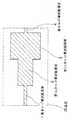
図1は、本発明の半導体光アンプの第1の実施の形態を示す。
図1に示す様に、本発明の半導体光アンプは、導波路構造および埋め込み(BH:Baried Heterostructure)構造を有しており、例えば、1.55μm帯で用いられる。その構成は、導波光に対して基本モードを提供する基本モード導波路領域1と、基本モード導波路領域1に接続されると共に前記導波光に対して多モードを含むモードを提供する第1の多モード導波路領域2と、この第1の多モード導波路領域2に接続されると共に多モードを含むモードを提供する第2の多モード導波路領域3とから構成される。基本モード導波路領域1の導波路幅をW1、第1の多モード導波路領域2の導波路幅をW2、第2の多モード導波路領域3の導波路幅をW3とすると、W3>W2>W1となるように導波路幅が設定される。尚、W4は基板21(または、デバイス)の幅である。このように、多モード導波路領域を複数にし、その導波路幅を出力側に向かって段階的に広くなるようにしたことにより、基本モード導波路の一部の導波路幅を段階的に広げた状態を形成できるようになり、高出力化を図るために必要な飽和出力レベルを改善できるようになる。
【0019】
第1および第2の多モード導波路領域2,3は、1×1−MMI(Multi Mode Interference :1入力1出力型のマルチモード干渉型導波路をいう)導波路として設計されている。各領域長(導波路長)は、基本モード導波路領域1が490μm程度、第1の多モード導波路領域2が75μm程度、第2の多モード導波路領域3が185μm程度であり、これを合計した共振器長は750μm程度となっている。
【0020】
上記第1の実施の形態は、1×1−MMIとして設計された第1の多モード導波路領域2が、基本モード導波路領域1と第2の多モード導波路領域3の間に設けられている。第1の多モード導波路領域2および第2の多モード導波路領域3は、多モード導波路でありながら、その両端においては基本モード光のみが伝搬する擬似的な基本モード導波路として機能する。したがって、基本モード導波路領域1から伝搬してきた基本モード光が第1の多モード導波路領域2の領域内で多モードに展開し、再び第1の多モード導波路領域2の端部で基本モードとして出力される。同様にして、第2の多モード導波路領域3においてもモード変換が行われ、第2の多モード導波路領域3からは基本モードが出力される。この結果、第1の多モード導波路領域2の利得飽和は、第2の多モード導波路領域3を基本モード導波路領域1に直接接続したときの基本モード導波路領域2内での利得飽和レベルに対して改善され、従来構成のアクティブMMI型半導体光アンプに比べ、飽和出力を高くすることが可能になる。さらに、空間的ホールバーニングを改善することも可能になり、安定した横モードを得ることができる。
【0021】
図1の構成の半導体光アンプにおいて、基本モード導波路領域1の後端面に半全反射(HR)コーティングを施し、第2の多モード導波路領域3の光出射端面に無反射(AR: Antireflection coated)コーティングを施せば半導体レーザを構成することができる。第1の多モード導波路領域2が挿入されていることにより、半導体光アンプの場合と同様に、高出力の半導体レーザを得ることが可能になる。
【0022】
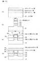
次に、上記第1の実施の形態の製造方法について説明する。
図2は、本発明による半導体光アンプの製造方法を示す。図中、(a)〜(d)は本発明の製造方法の代表的工程を示している。ここでは、第1の多モード導波路領域2の構造について示しているが、導波路幅Wが異なるのみで、基本モード導波路領域1も第2の多モード導波路領域3も同一構造である。基本モードと多モードの作り分けは、導波路の幅、導波路の長さ、材料の屈折率、および波長の各選択により可能である。また、図2においては、半導体光アンプの製造方法を示しているが、最終段階で基本モード導波路領域1の端面に半全反射(HR)コーティングを施し、第2の多モード導波路領域3の出射端面に無反射(AR)コーティングを施すことによって、半導体レーザを構成できることは上記した通りである。
【0023】
図2の(a)〜(d)を参照して本発明の半導体レーザの製造方法について説明する。まず、図2の(a)に示す様に、導波路幅W4のn−InP基板上21上にn−InPバッファ層22、1.55μm組成InGaAsP活性層23、およびp−InP第1クラッド層24をMOVPE法を用いて順次積層する。各層の層厚は、n−InPバッファ層22が100μm程度、1.55μm組成InGaAsP活性層23が300μm程度、p−InPクラッド層24が100μm程度である。ついで、通常のフォトリソグラフィ法およびウエットエッチング法を用いてメサ形成用マスク31を形成する。
【0024】
次に、図2の(b)に示す様に、マスク31の部分を残して、他の部分をRIE(Reactive Ion Etching:反応性イオンエッチング)法を用いてp−InPクラッド層24、1.55μm組成InGaAsP活性層23、n−InPバッファ層22、およびn−InP基板21の一部を除去し、メサを形成する。次に、図2の(c)に示す様に、(b)に示したメサの脇にp−InP電流ブロック層25とn−InP電流ブロック層26をMOVPE法により形成する。p−InP電流ブロック層25とn−InP電流ブロック層26の厚さは、共に1μm程度とする。
【0025】
次に、図2の(d)に示す様に、バッファードフッ酸でメサ形成用マスク31を除去した後、p−InP第2クラッド層27とp+InGaAsキャップ層28をMOVPE法により形成する。更に、裏面(図の底面)を研磨し、この裏面に通常のスパッタリング法により裏面電極および表面電極を形成する。また、素子劈開を行い、この劈開面に無反射(AR: antireflection coated)コーティングを施す。以上により半導体光アンプの製作が完了する。
【0026】
〔第2の実施の形態〕
図3は、本発明による半導体光アンプの第2の実施の形態を示す。
本実施の形態は、前記実施の形態と同様に、埋め込み(BH)構造型による1.55μm帯の半導体光アンプとしている。本実施の形態が図1に示した第1の実施の形態と異なるところは、図1に示した半導体光アンプの出射端、即ち、第2の多モード導波路領域3の出射端に、第2の基本モード導波路領域4を接続したところにある。なお、第2の基本モード導波路領域4は、基本モードのほか、擬似的基本モード導波路領域を用いることができる。第2の基本モード導波路領域4は、シングルモード導波路、1×1−MMI導波路、または1次モードを許容する導波路のいずれかを用いることができる。第2の基本モード導波路領域4を半導体光アンプの出射端に設けることにより、第2の多モード導波路領域3の長さを劈開位置によらず決定できるようになり、半導体光アンプの高歩留まり化が可能になる。
【0027】
図3に示す半導体光アンプの各領域長は、基本モード導波路領域1(第1の基本モード導波路領域)が460μm程度、1×1−MMI導波路領域2が75μm程度、1×1−MMI導波路領域3が185μm程度、第2の基本モード導波路領域4が30μm程度であり、これらを合計した共振器長は750μm程度である。
【0028】
図3に示した構成の半導体光アンプの製造方法は、上記第1の実施の形態と同じであるので、ここでは説明を省略する。活性層23は1.55μm組成InGaAsPで、p−InP電流ブロック層25およびn−InP電流ブロック層26による電流狭窄構造となっている。その上にp−InPクラッド層27およびp−InGaAs層28が積層され、層構造を成している。基本モード導波路領域1の導波路幅W1は0.5μm、第1の多モード導波路領域2の導波路幅W2は5μm、第2の多モード導波路領域3の導波路幅Wは38.5μmである。
【0029】
この第2の実施の形態においても、前記第1の実施の形態と同一の理由により高い飽和出力レベルを得ることができる。本実施の形態では、半導体アンプの出射端に微小な領域長を有すに第2の基本モード導波路領域4が付加されているが、その飽和出力は第2の基本モード導波路領域4によっては殆ど制約されない。これは、第2の基本モード導波路領域4による利得が、半導体光アンプ全体の利得に対して殆ど無視できるレベルであるためである。出射端に第2の基本モード導波路領域4を設けることによって、第2の多モード導波路領域3の長さが劈開位置によらず決定されるため、より高歩留まりに素子を提供することが可能になる。
【0030】
また、図3の半導体光アンプにおいても、基本モード導波路領域1(第1の基本モード導波路領域)の側端面に半反射(HR)コーティングを施し、第2の基本モード導波路領域4の光出射端面に無反射(AR: Antireflection coated)コーティングを施せば半導体レーザを構成でき、上記した理由により高出力の半導体レーザを得ることができる。
【0031】
尚、図3においては、第2の多モード導波路領域3に第2の基本モード導波路領域4を接続しているが、この基本モード導波路領域4は必ずしも基本モード導波路である必要はなく、1次モードを許容する導波路であっても、幅の異なる1×1−MMI導波路であってもよい。いずれを用いても基本モードおよび偏光無依存性は保たれる。
【0032】
〔第3の実施の形態〕
図4は、本発明による半導体光アンプの第3の実施の形態を示す。
図4は図1の構成において、第1の多モード導波路領域2を幅の異なるN個の導波路領域から構成されるようにしたものである。即ち、第1の多モード導波路領域2は、導波路領域2−1, 2−2, 2−3, ・・・2−NのN個(Nは2以上の整数)からなり、それぞれの導波路幅はW2−1, W2−2, W2−3, ・・・W2−Nは、W2−N>・・・>W2−3>W2−2>W2−1のように、後段(出力側)に向かうにつれて大きくなるように設定する。
【0033】
図4の様な構成により、半導体光アンプにおいては光増幅度を大きくすることができ、半導体レーザにおいては光パワーを増大させることができる。尚、N個の導波路領域に分割する構成は、第1の多モード導波路領域2に施すのが効果的であるが、同様の構成を第2の多モード導波路領域3に施すこともできる。
【0034】
尚、上記各実施の形態においては、半導体光アンプ(および半導体レーザ)を単純な埋め込み構造(BH構造)としたが、本発明はこの構造に限定されものではなく、他の層構造についても適用可能である。例えば、電流狭窄に優れるDC−PBH(doub1e channe1 p1anner buried heterostructure )構造の採用によっても本発明を達成することができる。また、半導体光アンプの波長は、1.55μm帯にしたが、勿論、本発明はこの値に限定されるものではなく、可視光帯域であってもよいし、0.98μm帯等の近赤外光帯であってもよい。
【0035】
さらに、以上の実施の形態においては、活性層をバルクとしているが、これに限定されるものではなく、例えば、MQW(Multi Quantum Well:複数量子井戸)構造であってもよい。製造方法についても、本実施例、およびこれから下記に述べる実施例2においては、結晶成長にMOVPE(Metal Organic Vapor Phase Epitaxial growth:有機金属気相成長)法、メサ形成方法にRIE法を用いたが、本発明はこれらに限定されるわけではない。例えば、結晶成長方法にはMBE(Molecular Beam Epitaxy:分子線エピタキシー)法を用いることができるし、メサ形成方法にはICP(Inductively Couple Plasma :誘導結合プラズマエッチング)法やウエットエッチング法を用いることができる。
【0036】
【発明の効果】
以上より明らかなように、本発明の半導体光アンプによれば、第1の多モード干渉導波路領域と第2の多モード干渉導波路領域の導波路幅が段階的に広くなるように設定した構成にしたことにより、結合部(接続部)に起因する特性の悪化を防止でき、基本モード特性および偏光依存性を維持したまま、飽和出力レベルの改善および高出力化が可能になる。
【0037】
また、本発明の他の半導体光アンプによれば、多モード干渉導波路領域が第1の多モード干渉導波路領域と第2の多モード干渉導波路領域を含み、第1の多モード干渉導波路領域と第2の多モード干渉導波路領域の導波路幅に差異を持たせ、さらに第1の多モード干渉導波路領域または第2の多モード干渉導波路領域を出力側に向かって順次導波路幅が大きくしながら複数に分割した構造にしているため、各結合部における影響を更に抑制することができる。この結果、結合部(接続部)に起因する特性の悪化を防止できるようになり、基本モード特性および偏光依存性を維持したまま、飽和出力レベルの改善および高出力化が可能になる。
【0038】
また、本発明の半導体レーザによれば、第1の多モード干渉導波路領域と第2の多モード干渉導波路領域の導波路幅が段階的に広くなるように設定されているため、結合部(接続部)に起因する特性の悪化を防止できる結果、基本モードにおいて高出力化が可能な半導体レーザを得ることができる。
【0039】
さらに、本発明の他の半導体レーザによれば、多モード干渉導波路領域が第1の多モード干渉導波路領域と第2の多モード干渉導波路領域を含み、第1の多モード干渉導波路領域と第2の多モード干渉導波路領域の導波路幅に差異を持たせ、更に第1の多モード干渉導波路領域または第2の多モード干渉導波路領域を出力側に向かって順次導波路幅が大きくしながら複数に分割した構造にしているため、各結合部における影響を更に抑制することができる。この結果、結合部(接続部)に起因する特性の悪化を防止できるようになり、基本モードにおいて高出力化が可能な半導体レーザを得ることができる。
【図面の簡単な説明】
【図1】本発明の半導体光アンプの第1の実施の形態を示す平面図である。
【図2】図1に示した第1の実施の形態の製造方法を示す断面図である。
【図3】本発明による半導体光アンプの第2の実施の形態を示す平面図である。
【図4】本発明による半導体光アンプの第3の実施の形態を示す平面図である。
【符号の説明】
1 基本モード導波路領域
2 第1の多モード導波路領域
3 第2の多モード導波路領域
4 第2の基本モード導波路領域
21 n−InP基板
22 n−InPバッファー層
23 1.55組成InGaAsP層
24 p−InPクラッド層
25 p−InP電流ブロック層
26 n−InP電流ブロック層
27 p−InP第2クラッド層
28 p+InGaAsPキャップ層
31 メサ形成用マスク[0001]
BACKGROUND OF THE INVENTION
The present invention relates to a semiconductor optical amplifier and a semiconductor laser, and more particularly to a semiconductor optical amplifier with improved saturation output and a semiconductor laser with high output and maximum output.
[0002]
[Prior art]
A semiconductor optical amplifier has the following features: (1) its size is smaller than other optical amplifiers, (2) it can be integrated with other functional devices, and (3) it can realize new functions. have. For this reason, research and development is actively underway. Waveguide-type semiconductor optical amplifiers are premised on the propagation of information by placing signals on light, and the waveguide structure is designed so that the fundamental mode condition is satisfied or the fundamental mode is simulated. It is common to do. The reason is to avoid the problem that if the signal light is made multimode, it is affected by multimode dispersion, or it becomes difficult to efficiently connect the signal light to another optical waveguide such as an optical fiber or a lens. is there.
[0003]
However, there is a problem that the laser characteristics are limited if the design is made so as to satisfy the fundamental mode in a pseudo manner. For example, in a semiconductor laser, the width and thickness of the active layer are limited by fundamental mode conditions. For example, the simplest method for improving the gain saturation level is to widen the waveguide width. However, since this method is restricted by the fundamental mode conditions described above, there is a limit to increasing the output.
[0004]
Therefore, Japanese Patent Application Laid-Open No. 11-132798 proposes a configuration of a semiconductor optical amplifier that eliminates the polarization dependency and avoids the restriction due to the fundamental mode condition. The semiconductor optical amplifier disclosed in this publication is an active MMI (Active Multi Mode Interference) type semiconductor optical amplifier, which is a method of improving the saturation output level by arranging a 1 × 1-MMI waveguide near the output end. is there. However, when the saturation output level is improved by 10 dB or more by this method, the problem of gain saturation near the output end is solved, but gain saturation in the single mode waveguide near the MMI waveguide newly restricts the saturation output level. Will do.
[0005]
Furthermore, Japanese Unexamined Patent Publication No. 2000-323781 discloses a semiconductor optical amplifier having a configuration in which a fundamental mode waveguide and a multimode waveguide having a wider waveguide width than the fundamental mode waveguide are connected to the fundamental mode waveguide, and Semiconductor lasers have been proposed. By connecting a multimode waveguide with a wide waveguide width to the fundamental mode waveguide, the same effect as widening the waveguide width in part of the fundamental mode waveguide region can be achieved, and the fundamental mode conditions can be changed. This makes it possible to improve the gain saturation level (saturation output level). As a result, high output is obtained for a semiconductor optical amplifier, and improvement of COD (end face optical damage) level and spatial hole burning for semiconductor lasers, prevention of efficiency reduction due to mode conversion loss, and mode stability. It becomes possible to improve.
[0006]
[Problems to be solved by the invention]
However, according to the conventional semiconductor optical amplifier, in the active MMI type optical amplifier disclosed in Japanese Patent Application Laid-Open No. 11-132798, the gain in the fundamental mode waveguide near the MMI waveguide is assumed when the saturation output improvement of 10 dB or more is assumed. There is a problem that saturation becomes significant and restricts the saturation output level. In addition, since the same phenomenon occurs, a similar problem occurs in a conventional actuated MMI type semiconductor laser in which a high reflectivity film is provided on the rear end face and a low reflectivity film is provided on the front end face.
[0007]
Furthermore, in Japanese Patent Application Laid-Open No. 2000-323781, a multimode waveguide region is provided based on the idea of widening the waveguide width as much as possible in order to improve the saturation level while considering reduction of power consumption. As a result, the difference in waveguide width becomes large, and for a strong incident light, gain saturation becomes noticeable by providing a multimode waveguide region, and the expected performance may not be obtained. .
[0008]
Accordingly, an object of the present invention is to provide a semiconductor optical amplifier capable of improving the saturation output of an active MMI optical amplifier and increasing the output.
[0009]
Another object of the present invention is to provide a semiconductor laser capable of obtaining a higher output than an active MMI type semiconductor laser.
[0010]
[Means for Solving the Problems]
In order to achieve the above object, the present invention has, as a first feature, a fundamental mode waveguide region that provides a fundamental mode for guided light, and a waveguide width wider than the fundamental mode waveguide region. A first multimodeinterference waveguide region connected to the fundamental mode waveguide region and providing a mode including a multimode with respect to the guided light; and a wider guide than the first multimodeinterference waveguide region. It has a waveguide width, which is connected to the first multimodeinterference waveguide region of, a semiconductor optical amplifier, characterized in that it comprises a second multi-modeinterference waveguide region that provides modes including multimode .
[0011]
According to this configuration, since the waveguide widths of the first multimodeinterference waveguide region and the second multimodeinterference waveguide region are set to increase stepwise, the coupling portion (connection portion) As a result, it is possible to prevent the deterioration of the resulting characteristics, and it is possible to improve the saturation output level and increase the output while maintaining the fundamental mode characteristics and polarization dependency.
[0012]
In order to achieve the above object, according to the present invention, as a second feature,a fundamental mode waveguide region that provides a fundamental mode for guided light, and a waveguide width wider than the fundamental mode waveguide region are provided. A first multimode interference waveguide region that is connected to the fundamental mode waveguide region and provides a mode including a multimode with respect to the emitted light; and more than the first multimode interference waveguide region A second multimode interference waveguide region having a wide waveguide width, connected to the first multimode interference waveguide region, and providing a mode including a multimode, the first multimode interference The semiconductor optical amplifier ischaracterized in that the waveguide region or the second multimode interference waveguide region is divided into a plurality of waveguide regions whose waveguide widths are sequentially increased toward the output side .
[0013]
According to this configuration, the multi-modeinterference waveguide region comprises a first multimodeinterference waveguide region and the second multimodeinterference waveguide region of the first multi-modeinterference waveguide region and the second multi-mode ofA difference is made in the waveguide width of theinterference waveguide region, and a plurality of the first multimodeinterference waveguide region or the second multimodeinterference waveguide region are sequentially increased toward the output side while increasing the waveguide width. Since the structure is divided into two, the influence at each coupling portion can be further suppressed. As a result, it becomes possible to prevent the deterioration of characteristics due to the coupling portion (connection portion), and it is possible to improve the saturation output level and increase the output while maintaining the fundamental mode characteristics and polarization dependency.
[0014]
Furthermore, the present invention is to achieve the above object, a third aspect,the lowanti-go computing(A ntireflection coating) is performed on the front face with the total reflection coating is applied to the rear end face, guide A fundamental mode waveguide region that provides a fundamental mode for wave light, and a first multimode interference waveguide region that is connected to the fundamental mode waveguide region and provides a mode including multiple modes for the guided light; A second multimode interference waveguide having a wider waveguide width than the first multimode waveguide region and connected to the first multimode interference waveguide region to provide a mode including multiple modes A semiconductor laser comprising a region is provided.
[0015]
According to this configuration, since the waveguide widths of the first multimodeinterference waveguide region and the second multimodeinterference waveguide region are set to increase stepwise, the coupling portion (connection portion) As a result of preventing the deterioration of the resulting characteristics, it becomes possible to increase the output in the basic mode.
[0016]
The present invention, in order to achieve the above object, a fourth aspect,the lowanti-go computing(A ntireflection coating) is performed on the front end face with are subjected to total reflection coating on the rear surface, electrical A fundamental mode waveguide region that provides a fundamental mode for wave light, and a waveguide width wider than the fundamental mode waveguide region, connected to the fundamental mode waveguide region, and capable of providing multiple modes for guided light. A first multimode interference waveguide region that provides a mode including, a waveguide width wider than the first multimode interference waveguide region, and connected to the first multimode interference waveguide region; A second multimode interference waveguide region that provides a mode including a multimode, and the first multimode interference waveguide region or the second multimode interference waveguide region is sequentially directed toward the output side. Multiple waveguides with increased waveguide width To provide a semiconductor laser according to claim which is divided into the waveguide region.
[0017]
According to this configuration, the multi-modeinterference waveguide region comprises a first multimodeinterference waveguide region and the second multimodeinterference waveguide region of the first multi-modeinterference waveguide region and the second multi-mode ofA difference is made in the waveguide width of theinterference waveguide region, and the first multimodeinterference waveguide region or the second multimodeinterference waveguide region is made to be plural while the waveguide width is sequentially increased toward the output side. Since the structure is divided, it is possible to further suppress the influence at each coupling portion. As a result, it becomes possible to prevent the deterioration of the characteristics due to the coupling portion (connection portion), and it is possible to increase the output in the basic mode.
[0018]
DETAILED DESCRIPTION OF THE INVENTION
Hereinafter, embodiments of the present invention will be described with reference to the drawings.
[First Embodiment]
FIG. 1 shows a semiconductor optical amplifier according to a first embodiment of the present invention.
As shown in FIG. 1, the semiconductor optical amplifier of the present invention has a waveguide structure and a buried (BH) structure, and is used in a 1.55 μm band, for example. The configuration includes a fundamental mode waveguide region 1 that provides a fundamental mode for guided light, and a first mode that is connected to the fundamental mode waveguide region 1 and provides a mode including multiple modes for the guided light. The
[0019]
The first and second
[0020]
In the first embodiment, the first
[0021]
In the semiconductor optical amplifier having the configuration shown in FIG. 1, a semi-total reflection (HR) coating is applied to the rear end face of the fundamental mode waveguide region 1, and no reflection (AR) is applied to the light exit end face of the second
[0022]
Next, the manufacturing method of the first embodiment will be described.
FIG. 2 shows a method of manufacturing a semiconductor optical amplifier according to the present invention. In the figure, (a) to (d) show typical steps of the production method of the present invention. Here, the structure of the first
[0023]
The semiconductor laser manufacturing method of the present invention will be described with reference to FIGS. First, as shown in FIG. 2A, an n-
[0024]
Next, as shown in FIG. 2 (b), the p-InP clad layers 24, 1... Are left using the RIE (Reactive Ion Etching) method while leaving the portion of the
[0025]
Next, as shown in FIG. 2D, after removing the
[0026]
[Second Embodiment]
FIG. 3 shows a second embodiment of the semiconductor optical amplifier according to the present invention.
In the present embodiment, a 1.55 μm band semiconductor optical amplifier of a buried (BH) structure type is used, as in the above embodiment. This embodiment differs from the first embodiment shown in FIG. 1 in that the output end of the semiconductor optical amplifier shown in FIG. 1, that is, the output end of the second
[0027]
Each region length of the semiconductor optical amplifier shown in FIG. 3 is about 460 μm in the fundamental mode waveguide region 1 (first fundamental mode waveguide region), and about 75 μm in the 1 × 1-
[0028]
Since the method for manufacturing the semiconductor optical amplifier having the configuration shown in FIG. 3 is the same as that of the first embodiment, the description thereof is omitted here. The
[0029]
Also in the second embodiment, a high saturation output level can be obtained for the same reason as in the first embodiment. In the present embodiment, the second fundamental mode waveguide region 4 is added so as to have a very small region length at the output end of the semiconductor amplifier, but the saturation output is generated by the second fundamental mode waveguide region 4. Are almost unconstrained. This is because the gain by the second fundamental mode waveguide region 4 is at a level that can be almost ignored with respect to the gain of the entire semiconductor optical amplifier. By providing the second fundamental mode waveguide region 4 at the emission end, the length of the second
[0030]
Also in the semiconductor optical amplifier of FIG. 3, the side end face of the fundamental mode waveguide region 1 (first fundamental mode waveguide region) is subjected to semi-reflective (HR) coating, so that the second fundamental mode waveguide region 4 A semiconductor laser can be constructed by applying antireflection coated (AR) coating on the light emitting end face, and a high-power semiconductor laser can be obtained for the reasons described above.
[0031]
In FIG. 3, the second fundamental mode waveguide region 4 is connected to the second
[0032]
[Third Embodiment]
FIG. 4 shows a third embodiment of a semiconductor optical amplifier according to the present invention.
FIG. 4 shows the configuration of FIG. 1 in which the first
[0033]
With the configuration as shown in FIG. 4, the optical amplification can be increased in the semiconductor optical amplifier, and the optical power can be increased in the semiconductor laser. In addition, although it is effective to apply the configuration divided into N waveguide regions to the first
[0034]
In each of the above embodiments, the semiconductor optical amplifier (and the semiconductor laser) has a simple buried structure (BH structure). However, the present invention is not limited to this structure, and can be applied to other layer structures. Is possible. For example, the present invention can also be achieved by adopting a DC-PBH (doub1 channel 1 p1anner buried heterostructure) structure excellent in current confinement. The wavelength of the semiconductor optical amplifier is in the 1.55 μm band, but the present invention is of course not limited to this value, and may be in the visible light band or in the near red region such as the 0.98 μm band. It may be an outside light band.
[0035]
Furthermore, in the above embodiment, the active layer is a bulk, but is not limited to this, and may be, for example, an MQW (Multi Quantum Well) structure. As for the manufacturing method, in this example and in Example 2 described below, the MOVPE (Metal Organic Vapor Phase Epitaxial Growth) method was used for crystal growth, and the RIE method was used for the mesa formation method. However, the present invention is not limited to these. For example, MBE (Molecular Beam Epitaxy) method can be used for the crystal growth method, and ICP (Inductively Couple Plasma) method or wet etching method can be used for the mesa formation method. it can.
[0036]
【The invention's effect】
As is clear from the above, according to the semiconductor optical amplifier of the present invention, the waveguide widths of the first multimodeinterference waveguide region and the second multimodeinterference waveguide region are set to be gradually increased. By adopting the configuration, it is possible to prevent the deterioration of characteristics due to the coupling portion (connection portion), and it is possible to improve the saturation output level and increase the output while maintaining the fundamental mode characteristics and polarization dependency.
[0037]
According to another semiconductor optical amplifier of the present invention, the multi-modeinterference waveguide region comprises a first multimodeinterference waveguide region and the second multimodeinterference waveguide region of the first multi-modeinterference guide The waveguide width is different from that of the second multimodeinterference waveguide region, and the first multimodeinterference waveguide region or the second multimodeinterference waveguide region is sequentially guided toward the output side. Since the waveguide width is increased and the structure is divided into a plurality of parts, the influence at each coupling portion can be further suppressed. As a result, it becomes possible to prevent the deterioration of characteristics due to the coupling portion (connection portion), and it is possible to improve the saturation output level and increase the output while maintaining the fundamental mode characteristics and polarization dependency.
[0038]
In addition, according to the semiconductor laser of the present invention, since the waveguide widths of the first multimodeinterference waveguide region and the second multimodeinterference waveguide region are set to increase stepwise, the coupling portion As a result of preventing the deterioration of characteristics due to (connecting portion), a semiconductor laser capable of increasing the output in the basic mode can be obtained.
[0039]
According to still another semiconductor laser of the present invention, the multi-modeinterference waveguide region comprises a first multimodeinterference waveguide region and the second multimodeinterference waveguide region of the first multi-modeinterference waveguide The waveguide width of the region and the second multimodeinterference waveguide region are different, and the first multimodeinterference waveguide region or the second multimodeinterference waveguide region is sequentially guided toward the output side. Since the structure is divided into a plurality of parts while increasing the width, the influence at each coupling portion can be further suppressed. As a result, it is possible to prevent the deterioration of characteristics due to the coupling portion (connection portion), and it is possible to obtain a semiconductor laser capable of increasing the output in the basic mode.
[Brief description of the drawings]
FIG. 1 is a plan view showing a first embodiment of a semiconductor optical amplifier according to the present invention.
FIG. 2 is a cross-sectional view showing the manufacturing method of the first embodiment shown in FIG.
FIG. 3 is a plan view showing a second embodiment of a semiconductor optical amplifier according to the present invention.
FIG. 4 is a plan view showing a third embodiment of a semiconductor optical amplifier according to the present invention.
[Explanation of symbols]
DESCRIPTION OF SYMBOLS 1 Basic mode waveguide area |
Claims (12)
Translated fromJapanese前記基本モード導波路領域よりも広い導波路幅を有し、前記基本モード導波路領域に接続され、前記導波光に対して多モードを含むモードを提供する第1の多モード干渉導波路領域と、
前記第1の多モード干渉導波路領域よりも広い導波路幅を有し、前記第1の多モード干渉導波路領域に接続され、多モードを含むモードを提供する第2の多モード干渉導波路領域を備えることを特徴とする半導体光アンプ。A fundamental mode waveguide region that provides a fundamental mode for guided light;
A first multimode interference waveguide region that has a wider waveguide width than the fundamental mode waveguide region, is connected to the fundamental mode waveguide region, and provides a mode including multiple modes for the guided light; ,
Second multimode interference waveguide having a wider waveguide width than the first multimode interference waveguide region, connected to the first multimode interference waveguide region, and providing a mode including multiple modes A semiconductor optical amplifier comprising a region.
前記基本モード導波路領域よりも広い導波路幅を有し、前記基本モード導波路領域に接続され、前記出射光に対して多モードを含むモードを提供する第1の多モード干渉導波路領域と、
前記第1の多モード干渉導波路領域よりも広い導波路幅を有し、前記第1の多モード干渉導波路領域に接続され、多モードを含むモードを提供する第2の多モード干渉導波路領域とを備え、
前記第1の多モード干渉導波路領域または前記第2の多モード干渉導波路領域は、出力側に向かって順次導波路幅を大きくした複数の導波路領域に分割されていることを特徴とする半導体光アンプ。A fundamental mode waveguide region that provides a fundamental mode for guided light;
A first multimode interference waveguide region that has a wider waveguide width than the fundamental mode waveguide region, is connected to the fundamental mode waveguide region, and provides a mode including multiple modes for the emitted light; ,
Second multimode interference waveguide having a wider waveguide width than the first multimode interference waveguide region, connected to the first multimode interference waveguide region, and providing a mode including multiple modes With areas,
The first multimode interference waveguide region or the second multimode interference waveguide region is divided into a plurality of waveguide regions whose waveguide widths are sequentially increased toward the output side. Semiconductor optical amplifier.
前記基本モード導波路領域に接続されると共に導波光に対して多モードを含むモードを提供する第1の多モード干渉導波路領域と、
前記第1の多モード導波路領域よりも広い導波路幅を有し、前記第1の多モード干渉導波路領域に接続されて多モードを含むモードを提供する第2の多モード干渉導波路領域を備えることを特徴とする半導体レーザ。A fundamental mode waveguide region to provide a fundamental modelow reactiongo computing(A ntireflection coating) is applied to the front surface, with respect to the guided light with total reflection coating is applied on the rear end face,
A first multimode interference waveguide region connected to the fundamental mode waveguide region and providing a mode including multimodes for guided light;
A second multimode interference waveguide region having a wider waveguide width than the first multimode waveguide region and connected to the first multimode interference waveguide region to provide a mode including multiple modes A semiconductor laser comprising:
前記基本モード導波路領域よりも広い導波路幅を有し、前記基本モード導波路領域に接続され、導波光に対して多モードを含むモードを提供する第1の多モード干渉導波路領域と、
前記第1の多モード干渉導波路領域よりも広い導波路幅を有し、前記第1の多モード干渉導波路領域に接続され、多モードを含むモードを提供する第2の多モード干渉導波路領域とを備え、
前記第1の多モード干渉導波路領域または前記第2の多モード干渉導波路領域は、出力側に向かって順次導波路幅を大きくした複数の導波路領域に分割されていることを特徴とする半導体レーザ。A fundamental mode waveguide region to provide a fundamental modelow reactiongo computing(A ntireflection coating) is applied to the front surface, with respect to the guided light with are subjected to total reflection coating on the rear end face,
A first multimode interference waveguide region that has a wider waveguide width than the fundamental mode waveguide region, is connected to the fundamental mode waveguide region, and provides a mode including multiple modes for guided light;
Second multimode interference waveguide having a wider waveguide width than the first multimode interference waveguide region, connected to the first multimode interference waveguide region, and providing a mode including multiple modes With areas,
The first multimode interference waveguide region or the second multimode interference waveguide region is divided into a plurality of waveguide regions whose waveguide widths are sequentially increased toward the output side. Semiconductor laser.
Priority Applications (2)
| Application Number | Priority Date | Filing Date | Title |
|---|---|---|---|
| JP2001125210AJP3991615B2 (en) | 2001-04-24 | 2001-04-24 | Semiconductor optical amplifier and semiconductor laser |
| US10/127,557US6813068B2 (en) | 2001-04-24 | 2002-04-23 | Semiconductor optical amplifier and semiconductor laser |
Applications Claiming Priority (1)
| Application Number | Priority Date | Filing Date | Title |
|---|---|---|---|
| JP2001125210AJP3991615B2 (en) | 2001-04-24 | 2001-04-24 | Semiconductor optical amplifier and semiconductor laser |
Publications (2)
| Publication Number | Publication Date |
|---|---|
| JP2002319741A JP2002319741A (en) | 2002-10-31 |
| JP3991615B2true JP3991615B2 (en) | 2007-10-17 |
Family
ID=18974469
Family Applications (1)
| Application Number | Title | Priority Date | Filing Date |
|---|---|---|---|
| JP2001125210AExpired - Fee RelatedJP3991615B2 (en) | 2001-04-24 | 2001-04-24 | Semiconductor optical amplifier and semiconductor laser |
Country Status (2)
| Country | Link |
|---|---|
| US (1) | US6813068B2 (en) |
| JP (1) | JP3991615B2 (en) |
Families Citing this family (22)
| Publication number | Priority date | Publication date | Assignee | Title |
|---|---|---|---|---|
| US6791746B2 (en)* | 2002-02-12 | 2004-09-14 | Finisar Corporation | Extended bandwidth semiconductor optical amplifier |
| EP1372229B1 (en)* | 2002-06-12 | 2006-02-15 | Agilent Technologies Inc., A Delaware Corporation | Integrated semiconductor laser and waveguide device |
| EP1372228B1 (en)* | 2002-06-12 | 2006-10-04 | Agilent Technologies, Inc. - a Delaware corporation - | Integrated semiconductor laser and waveguide device |
| JPWO2005031829A1 (en)* | 2003-09-24 | 2006-12-07 | 日本電気株式会社 | Semiconductor device and semiconductor integrated device |
| EP1710876B1 (en)* | 2003-12-22 | 2009-12-02 | Panasonic Corporation | Semiconductor laser device and laser projector |
| JP4582289B2 (en)* | 2003-12-26 | 2010-11-17 | 日本電気株式会社 | Semiconductor laser |
| JP4423668B2 (en)* | 2004-05-26 | 2010-03-03 | 日立化成工業株式会社 | Optical waveguide |
| US7466736B2 (en) | 2004-08-13 | 2008-12-16 | Nec Corporation | Semiconductor laser diode, semiconductor optical amplifier, and optical communication device |
| JP4505470B2 (en)* | 2005-01-20 | 2010-07-21 | 富士通株式会社 | Optical waveguide device and semiconductor device |
| US7375812B2 (en)* | 2005-02-22 | 2008-05-20 | Axsun Technologies, Inc. | Method and system for reducing parasitic spectral noise in tunable semiconductor source spectroscopy system |
| US7184207B1 (en)* | 2005-09-27 | 2007-02-27 | Bookham Technology Plc | Semiconductor optical device |
| JP4657337B2 (en)* | 2008-09-29 | 2011-03-23 | シャープ株式会社 | Semiconductor laser device |
| JP4444368B1 (en)* | 2009-07-30 | 2010-03-31 | 古河電気工業株式会社 | Integrated semiconductor laser device, semiconductor laser module, and optical transmission system |
| JP5870509B2 (en)* | 2011-05-30 | 2016-03-01 | ソニー株式会社 | Light source device, optical pickup, recording device |
| US9166369B2 (en)* | 2013-04-09 | 2015-10-20 | Nlight Photonics Corporation | Flared laser oscillator waveguide |
| WO2018096522A1 (en) | 2016-11-28 | 2018-05-31 | King Abdullah University Of Science And Technology | Integrated semiconductor optical amplifier and laser diode at visible wavelength |
| CN109560465A (en)* | 2017-09-26 | 2019-04-02 | 北京万集科技股份有限公司 | A kind of 1x1 type single-chip integration formula semiconductor main oscillations amplifier |
| CN109560464A (en)* | 2017-09-26 | 2019-04-02 | 北京万集科技股份有限公司 | A kind of 1xN type single-chip integration formula semiconductor main oscillations amplifier |
| CN107910746B (en)* | 2017-11-08 | 2019-05-14 | 华中科技大学 | A kind of reflective semiconductor optical amplifier |
| CN110187589A (en)* | 2019-06-05 | 2019-08-30 | 中国科学院长春光学精密机械与物理研究所 | A semiconductor optical amplifier |
| US11837838B1 (en)* | 2020-01-31 | 2023-12-05 | Freedom Photonics Llc | Laser having tapered region |
| US11988872B2 (en)* | 2021-11-29 | 2024-05-21 | Ciena Corporation | Optical waveguide coupling using fabricated waveguide coupling structures |
Family Cites Families (24)
| Publication number | Priority date | Publication date | Assignee | Title |
|---|---|---|---|---|
| US3467906A (en)* | 1967-06-14 | 1969-09-16 | Rca Corp | Constant-gain low-noise light amplifier |
| US4794346A (en)* | 1984-11-21 | 1988-12-27 | Bell Communications Research, Inc. | Broadband semiconductor optical amplifier structure |
| US5175643A (en)* | 1991-09-30 | 1992-12-29 | Xerox Corporation | Monolithic integrated master oscillator power amplifier |
| US5260822A (en)* | 1992-01-31 | 1993-11-09 | Massachusetts Institute Of Technology | Tapered semiconductor laser gain structure with cavity spoiling grooves |
| US5539571A (en)* | 1992-09-21 | 1996-07-23 | Sdl, Inc. | Differentially pumped optical amplifer and mopa device |
| US5793521A (en)* | 1992-09-21 | 1998-08-11 | Sdl Inc. | Differentially patterned pumped optical semiconductor gain media |
| US5392308A (en)* | 1993-01-07 | 1995-02-21 | Sdl, Inc. | Semiconductor laser with integral spatial mode filter |
| DE69407312T2 (en)* | 1993-01-07 | 1998-07-23 | Nippon Electric Co | Integrated semiconductor optical device and manufacturing method |
| US5321718A (en)* | 1993-01-28 | 1994-06-14 | Sdl, Inc. | Frequency converted laser diode and lens system therefor |
| JP2817769B2 (en)* | 1994-12-28 | 1998-10-30 | 日本電気株式会社 | Optical amplifying device, semiconductor laser device using the same, and driving method thereof |
| JP3558717B2 (en)* | 1995-02-07 | 2004-08-25 | 富士通株式会社 | Laser diode, manufacturing method thereof, and optical communication system using such laser diode |
| US5936991A (en)* | 1996-09-17 | 1999-08-10 | The United States Of America As Represented By The Secretary Of The Air Force | Near fields in flared MOPAs amplifiers and oscillators by lateral current tailoring |
| DE69704544T2 (en)* | 1996-12-26 | 2001-11-29 | Nec Corp., Tokio/Tokyo | Optical semiconductor amplifier |
| JP3244115B2 (en)* | 1997-08-18 | 2002-01-07 | 日本電気株式会社 | Semiconductor laser |
| JP3244114B2 (en) | 1997-08-18 | 2002-01-07 | 日本電気株式会社 | Semiconductor optical amplifier |
| JP3153503B2 (en) | 1997-10-31 | 2001-04-09 | ニチハ株式会社 | Liquid supply volume measurement system |
| JPH11307862A (en)* | 1998-04-21 | 1999-11-05 | Nec Corp | Semiconductor laser |
| US6246709B1 (en)* | 1998-06-01 | 2001-06-12 | Oki Electric Industry Co., Ltd. | Integrated optical element and method for manufacturing an integrated optical element |
| US6381380B1 (en)* | 1998-06-24 | 2002-04-30 | The Trustees Of Princeton University | Twin waveguide based design for photonic integrated circuits |
| US6512629B1 (en)* | 1999-03-22 | 2003-01-28 | Genoa Corporation | Low-noise, high-power optical amplifier |
| JP3329764B2 (en) | 1999-05-13 | 2002-09-30 | 日本電気株式会社 | Semiconductor laser and semiconductor optical amplifier |
| US6330378B1 (en)* | 2000-05-12 | 2001-12-11 | The Trustees Of Princeton University | Photonic integrated detector having a plurality of asymmetric waveguides |
| JP4789320B2 (en)* | 2000-12-01 | 2011-10-12 | 富士通株式会社 | Semiconductor optical amplifier |
| GB2371145A (en)* | 2001-01-13 | 2002-07-17 | Kamelian Ltd | Semiconductor optical amplifier |
- 2001
- 2001-04-24JPJP2001125210Apatent/JP3991615B2/ennot_activeExpired - Fee Related
- 2002
- 2002-04-23USUS10/127,557patent/US6813068B2/ennot_activeExpired - Fee Related
Also Published As
| Publication number | Publication date |
|---|---|
| US6813068B2 (en) | 2004-11-02 |
| JP2002319741A (en) | 2002-10-31 |
| US20020154393A1 (en) | 2002-10-24 |
Similar Documents
| Publication | Publication Date | Title |
|---|---|---|
| JP3991615B2 (en) | Semiconductor optical amplifier and semiconductor laser | |
| EP1052747B1 (en) | Single mode semiconductor laser | |
| JP5387671B2 (en) | Semiconductor laser and integrated device | |
| JP3985159B2 (en) | Gain clamp type semiconductor optical amplifier | |
| US6445722B2 (en) | Single-transverse-mode laser diode with multi-mode waveguide region and manufacturing method of the same | |
| US9088132B2 (en) | Semiconductor optical element, integrated semiconductor optical element, and semiconductor optical element module | |
| JP2001308451A (en) | Semiconductor light emitting device | |
| US7045374B2 (en) | Method for manufacturing semiconductor optical amplifier having planar buried heterostructure | |
| US7466736B2 (en) | Semiconductor laser diode, semiconductor optical amplifier, and optical communication device | |
| JP3766637B2 (en) | Optical coupling element and optical device | |
| JP3017869B2 (en) | Semiconductor optical amplifier | |
| JP5616629B2 (en) | High brightness light emitting diode | |
| CN112072461A (en) | Electroabsorption modulated laser and manufacturing method thereof | |
| JP4453937B2 (en) | Optical integrated device and manufacturing method thereof | |
| US12259561B2 (en) | Spot-size converter | |
| JPH11223739A (en) | Integrated optical circuit device and method of manufacturing the same | |
| JPH0230195B2 (en) | ||
| WO2024236697A1 (en) | Optical semiconductor element | |
| JPH11307862A (en) | Semiconductor laser | |
| JP2010171098A (en) | Waveguide-type optical functional device and manufacturing method thereof | |
| JP2000049420A (en) | Semiconductor optical function device and method of manufacturing the same | |
| JPH0964460A (en) | Distributed feedback semiconductor laser |
Legal Events
| Date | Code | Title | Description |
|---|---|---|---|
| A621 | Written request for application examination | Free format text:JAPANESE INTERMEDIATE CODE: A621 Effective date:20040426 | |
| A977 | Report on retrieval | Free format text:JAPANESE INTERMEDIATE CODE: A971007 Effective date:20070213 | |
| A131 | Notification of reasons for refusal | Free format text:JAPANESE INTERMEDIATE CODE: A131 Effective date:20070220 | |
| A521 | Written amendment | Free format text:JAPANESE INTERMEDIATE CODE: A523 Effective date:20070416 | |
| A131 | Notification of reasons for refusal | Free format text:JAPANESE INTERMEDIATE CODE: A131 Effective date:20070529 | |
| A521 | Written amendment | Free format text:JAPANESE INTERMEDIATE CODE: A523 Effective date:20070619 | |
| TRDD | Decision of grant or rejection written | ||
| A01 | Written decision to grant a patent or to grant a registration (utility model) | Free format text:JAPANESE INTERMEDIATE CODE: A01 Effective date:20070703 | |
| A61 | First payment of annual fees (during grant procedure) | Free format text:JAPANESE INTERMEDIATE CODE: A61 Effective date:20070716 | |
| R150 | Certificate of patent or registration of utility model | Free format text:JAPANESE INTERMEDIATE CODE: R150 | |
| FPAY | Renewal fee payment (event date is renewal date of database) | Free format text:PAYMENT UNTIL: 20100803 Year of fee payment:3 | |
| A521 | Written amendment | Free format text:JAPANESE INTERMEDIATE CODE: A523 Effective date:20070416 | |
| FPAY | Renewal fee payment (event date is renewal date of database) | Free format text:PAYMENT UNTIL: 20110803 Year of fee payment:4 | |
| FPAY | Renewal fee payment (event date is renewal date of database) | Free format text:PAYMENT UNTIL: 20110803 Year of fee payment:4 | |
| FPAY | Renewal fee payment (event date is renewal date of database) | Free format text:PAYMENT UNTIL: 20120803 Year of fee payment:5 | |
| FPAY | Renewal fee payment (event date is renewal date of database) | Free format text:PAYMENT UNTIL: 20130803 Year of fee payment:6 | |
| LAPS | Cancellation because of no payment of annual fees |