JP3990167B2 - Liquid crystal display device driving method and liquid crystal display device using the driving method - Google Patents
Liquid crystal display device driving method and liquid crystal display device using the driving methodDownload PDFInfo
- Publication number
- JP3990167B2 JP3990167B2JP2002057274AJP2002057274AJP3990167B2JP 3990167 B2JP3990167 B2JP 3990167B2JP 2002057274 AJP2002057274 AJP 2002057274AJP 2002057274 AJP2002057274 AJP 2002057274AJP 3990167 B2JP3990167 B2JP 3990167B2
- Authority
- JP
- Japan
- Prior art keywords
- liquid crystal
- crystal display
- pulse width
- thin film
- display device
- Prior art date
- Legal status (The legal status is an assumption and is not a legal conclusion. Google has not performed a legal analysis and makes no representation as to the accuracy of the status listed.)
- Expired - Lifetime
Links
Images


Classifications
- G—PHYSICS
- G09—EDUCATION; CRYPTOGRAPHY; DISPLAY; ADVERTISING; SEALS
- G09G—ARRANGEMENTS OR CIRCUITS FOR CONTROL OF INDICATING DEVICES USING STATIC MEANS TO PRESENT VARIABLE INFORMATION
- G09G3/00—Control arrangements or circuits, of interest only in connection with visual indicators other than cathode-ray tubes
- G09G3/20—Control arrangements or circuits, of interest only in connection with visual indicators other than cathode-ray tubes for presentation of an assembly of a number of characters, e.g. a page, by composing the assembly by combination of individual elements arranged in a matrix no fixed position being assigned to or needed to be assigned to the individual characters or partial characters
- G09G3/34—Control arrangements or circuits, of interest only in connection with visual indicators other than cathode-ray tubes for presentation of an assembly of a number of characters, e.g. a page, by composing the assembly by combination of individual elements arranged in a matrix no fixed position being assigned to or needed to be assigned to the individual characters or partial characters by control of light from an independent source
- G09G3/36—Control arrangements or circuits, of interest only in connection with visual indicators other than cathode-ray tubes for presentation of an assembly of a number of characters, e.g. a page, by composing the assembly by combination of individual elements arranged in a matrix no fixed position being assigned to or needed to be assigned to the individual characters or partial characters by control of light from an independent source using liquid crystals
- G09G3/3611—Control of matrices with row and column drivers
- G09G3/3648—Control of matrices with row and column drivers using an active matrix
- G—PHYSICS
- G09—EDUCATION; CRYPTOGRAPHY; DISPLAY; ADVERTISING; SEALS
- G09G—ARRANGEMENTS OR CIRCUITS FOR CONTROL OF INDICATING DEVICES USING STATIC MEANS TO PRESENT VARIABLE INFORMATION
- G09G3/00—Control arrangements or circuits, of interest only in connection with visual indicators other than cathode-ray tubes
- G09G3/20—Control arrangements or circuits, of interest only in connection with visual indicators other than cathode-ray tubes for presentation of an assembly of a number of characters, e.g. a page, by composing the assembly by combination of individual elements arranged in a matrix no fixed position being assigned to or needed to be assigned to the individual characters or partial characters
- G09G3/2007—Display of intermediate tones
- G09G3/2014—Display of intermediate tones by modulation of the duration of a single pulse during which the logic level remains constant
Landscapes
- Engineering & Computer Science (AREA)
- Chemical & Material Sciences (AREA)
- Crystallography & Structural Chemistry (AREA)
- Physics & Mathematics (AREA)
- Computer Hardware Design (AREA)
- General Physics & Mathematics (AREA)
- Theoretical Computer Science (AREA)
- Liquid Crystal Display Device Control (AREA)
- Liquid Crystal (AREA)
- Control Of Indicators Other Than Cathode Ray Tubes (AREA)
Description
Translated fromJapanese【0001】
【発明の属する技術分野】
本発明は、アクティブマトリクス型液晶表示装置の駆動方法に関し、特に薄膜トランジスタをスイッチング素子に用いたパルス幅変調駆動方式の液晶表示装置の駆動方法およびその駆動方法により駆動する液晶表示装置に関する。
【0002】
【従来の技術】
パルス幅変調(PWM)方式により階調表示を行うアクティブマトリクス型液晶表示装置が知られている。PWM方式による液晶表示装置の駆動方法では、表示画素に印加する階調電圧の電圧レベルを表示階調に応じて変化させるのではなく、電圧の印加期間を表示階調に応じて変化させることにより、各階調に応じた表示を実現している。PWM駆動方式の液晶表示装置では、構成の簡単な階調電圧発生回路を用いつつ、表示階調数を増加させることができる。
【0003】
このようなPWM駆動方式の液晶表示装置の駆動方法について、特開平04-142592号公報で提案されているものを例に説明する。図6は、従来の液晶表示装置の主要部分を示すブロック図である。従来の液晶表示装置は、お互いに交差する複数の走査線101及び複数の信号線102、これらの交差部分に配列された複数の画素電極103、これらに接続され走査線101へのゲート信号及び信号線102へのデータ信号を受けてスイッチ動作する薄膜トランジスタ104が形成された液晶表示パネル100と、複数の走査線101にゲート信号を与える走査線駆動回路105と、複数の信号線102に各画素へ印加するデータ信号を与える信号線駆動回路106とを備えている。走査線駆動回路101は、1垂直期間内に複数の走査線101を順番に選択して複数の薄膜トランジスタをオンし、信号線駆動回路106はオンしている複数のトランジスタに接続された複数の画素電極104に対して、それぞれ表示階調に応じて決定したパルス幅の期間だけデータ信号を印加する。
【0004】
図7は、図6に示されるPWM駆動方式の液晶表示装置のある画素電極103に与えられる印加電圧VPの変化を示すタイミングチャートである。ある1垂直期間(1V)内に信号線102に与えられるデータ信号VDが基準レベルにあるときに、走査線101に与えられるゲート信号VGがハイレベルVGHになると、薄膜トランジスタ104はオンし、印加電圧VPはデータ信号VDにつられて上昇し、さらにデータ信号VDが正極性のアクティブレベルになると、表示階調に応じて決められたパルス幅の期間TW1だけ印加電圧VPはデータ信号につられて上昇する。次に、ゲート信号VGがローレベルVGLとなると薄膜トランジスタ104はオフし、このときの印加電圧VPを保持する。次の1垂直期間に信号線102に与えられるデータ信号VDが基準レベルにあるときに、走査線101に与えられるゲート信号VGがハイレベルVGHになると、薄膜トランジスタ104はオンし印加電圧VPはデータ信号VDにつられて低下し、さらにデータ信号VDが負極性のアクティブレベルになると、表示階調に応じて決められたパルス幅の期間TW2だけ印加電圧VPはデータ信号VDにつられて下降する。次に、ゲート信号VGがローレベルVGLとなると薄膜トランジスタ104はオフし、このときの印加電圧VPを保持する。このように、データ信号を表示階調に応じたパルス幅期間だけアクティブレベルにすることにより、構成の簡単な階調電圧発生回路を用いながら、多階調表示を実現している。
【0005】
特開平04-142592号公報では、書き込みを行うデータ極性で画素電極に印加される電圧が非対称になりチラツキ及び焼き付きが発生するのを防ぐため、データ信号が負極性の場合のゲートオン電圧をVGONN、正極性の場合のゲートオン電圧をVGONPとした場合、VGONNをVGONPより低く設定することも提案されている。
【0006】
【発明が解決しようとする課題】
ところで、このようなPWM駆動方式の液晶表示装置について、液晶表示パネルのパネル温度と表示特性について検討してみる。画素電極に接続されスイッチ動作をする薄膜トランジスタのオン電流はパネル温度に依存しており、パネル温度の上昇にともない増加する。液晶への印加電圧はオン電流とデータ信号パルス幅の積に比例するため、液晶表示パネルの表示階調−輝度特性がパネル温度に応じて変化する。そのため、パネル温度が変化すると液晶表示パネルの表示画質が変化する。また、薄膜トランジスタの電気的特性がパネル温度に依存するためデータ極性による書き込み量の非対称性はパネル温度により異なり、パネル温度が変化するとチラツキ及び焼き付きが発生する。
【0007】
したがって本発明の目的は、パネル温度の変化による表示階調−輝度特性の変化及び液晶表示パネルの焼き付きを抑制できるPWM方式の液晶表示装の駆動方法置及びその駆動方法により駆動される液晶表示装置を提供することにある。
【0008】
【課題を解決するための手段】
本発明によれば、薄膜トランジスタをスイッチング素子に用いたパルス幅変調方式により駆動するアクティブマトリクスタイプの液晶表示装置の駆動方法において、パネル温度検出手段を有し、ゲートオン電圧もしくはデータ信号パルス幅、基準クロック信号の周波数をパネル温度により補正すること、また、書き込みデータ極性によるゲートオン電圧の補正量もしくはデータ信号パルス幅の補正量をパネル温度により補正することを特徴とするアクティブマトリクス液晶表示装置の駆動方法およびその駆動方法により駆動される液晶表示装置が得られる。
【0009】
本発明の特徴は、薄膜トランジスタをスイッチング素子に用いたパルス幅変調駆動方式の液晶表示装置及びその駆動方法について、書き込みデータ極性に応じて液晶への印加電圧を補正すること、またこの補正を液晶表示パネルのパネル温度を考慮しつつ行うことを特徴とする。
【0010】
特徴の一つでは、パネル温度により、図3(a)のグラフに示される関係に沿って、ゲートオン電圧を補正しつつ液晶駆動を行うことにある。すなわち、図1の温度検出回路7からの制御信号により、DC/DCコンバータ4は、パネル温度が高いほど正極性及び負極性のゲートオン電圧を低くし、パネル温度が低いほど正極性及び負極性のゲートオン電圧を高く設定する。また、正極性のゲートオン電圧は負極性のゲートオン電圧よりも、常に高く設定する。
【0011】
さらに、他の特徴として、パネル温度により、図3(b)のグラフに示される関係に沿って、共通電圧中心VCOMセンタを補正しつつ液晶駆動を行う。すなわち、図1の温度検出回路7からの制御信号により、DC/DCコンバータ4は、パネル温度が高いほどVCOMセンタを高くし、パネル温度が低いほどVCOMセンタを低く設定する。
【0012】
このような液晶駆動により、データ信号VDを表示階調に応じたパルス幅期間だけアクティブレベルにするとともに、データ信号VDの極性に応じて供給されるゲート信号VGのゲートオン電圧を異ならせ、正極性ゲートオン電圧VGONPを負極性ゲートオン電圧VGONNより大きくしているので、薄膜トランジスタのオン電流IONを正極性データ書き込み時と負極性データ書き込み時とで等しくでき、書き込み非対称性を低減したPWM駆動を実現できる。
【0013】
さらに、このような関係を維持しつつ、パネル温度に応じて、図3(a)及び図3(b)に示される補正をゲートオン電圧及び共通電圧中心に対して行いつつ駆動することにより、パネル温度の変動によらず薄膜トランジスタのオン電流が一定となり表示階調−輝度特性のずれを低減できる。また、パネル温度の変動によるチラツキ及び焼き付きを低減できる。この結果、パネル温度の変化による液晶表示パネルの表示画質の変化を小さくすることができる。
【0014】
とくに本発明によれば、複数の画素電極にそれぞれ接続された複数のスイッチング用薄膜トランジスタ(TFT)を備えた液晶表示パネルをデータ信号のパルス幅変調駆動方式により駆動するアクティブマトリクスタイプの液晶表示装置(以下では、単にアクティブマトリクスタイプの液晶表示装置と呼ぶ)の駆動方法において、前記薄膜トランジスタの正極性ゲートオン電圧(VGONP)を負極性ゲートオン電圧(VGONN)よりも高く設定し、この関係を維持しつつ、所定の温度検出手段により検出した前記液晶表示パネルのパネル温度の上昇にともない正極性ゲートオン電圧(VGONP)および負極性ゲートオン電圧(VGONN)の両方をパネル温度の上昇前よりも低く設定することを特徴とする液晶表示装置の駆動方法が得られる。
【0015】
好ましくは、前記液晶表示パネルの共通電極に供給される共通電圧の中心(VCOMセンタ)をも前記パネル温度に基づいて設定する。
【0017】
また、複数の画素電極にそれぞれ接続された複数のスイッチング用薄膜トランジスタを備えた液晶表示パネルをデータ信号のパルス幅変調駆動方式により駆動するアクティブマトリクスタイプの液晶表示装置の駆動方法において、前記スイッチング用薄膜トランジスタのオン電流(I0N)が、所定の温度検出手段により検出した前記液晶表示パネルのパネル温度によらず一定となるように、所定の回路を用いて前記スイッチング用薄膜トランジスタの正極性ゲートオン電圧(VGONP)および負極性ゲートオン電圧(VGONN)を設定し、全表示階調におけるデータ信号の正極性データパルス幅(TWP)を負極性データパルス幅(TWN)よりも長く設定することをも特徴とする液晶表示装置の駆動方法が得られる。
【0018】
さらには、前記液晶表示パネルには、前記スイッチング用薄膜トランジスタと同時に液晶表示パネルに形成されたモニター用薄膜トランジスタを用いて、前記スイッチング用薄膜トランジスタのオン電流(I0N)が、前記液晶表示パネルのパネル温度によらず一定となるように前記スイッチング用薄膜トランジスタの正極性ゲートオン電圧(VGONP)および負極性ゲートオン電圧(VGONN)を設定し、全表示階調における前記データ信号の正極性データパルス幅(TWP)を前記負極性データパルス幅(TWN)よりも長く設定ことをも特徴とする液晶表示装置の駆動方法が得られる。
【0019】
また、本発明によれば、上記アクティブマトリクスタイプの液晶表示装置の駆動方法において、全表示階調における前記データ信号の正極性データパルス幅(TWP)を負極性データパルス幅(TWN)よりも長く設定し、所定の温度検出手段により検出した液晶表示パネルのパネル温度の上昇にともない前記薄膜トランジスタの正極性ゲートオン電圧(VGONP)および負極性ゲートオン電圧(VGONN)を低く設定することを特徴とする液晶表示装置の駆動方法が得られる。
【0021】
また、上記駆動方法において、全表示階調における前記データ信号の正極性データパルス幅(TWP)を負極性データパルス幅(TWN)よりも長く設定し、この関係を維持しつつ、所定の温度検出手段により検出した前記液晶表示パネルのパネル温度の上昇により前記正極性データパルス幅(TWP)および前記負極性データパルス幅(TWN)の両方を前記パネル温度の上昇前よりも短くすることを特徴とする液晶表示装置の駆動方法も得られる。
【0022】
さらに本発明によれば、上記駆動方法において、データ信号の正極性データパルス幅(TWP)を負極性データパルス幅(TWN)よりも長く設定し、この関係を維持しつつ、各表示階調をクロック数で与え、カウンタにより基準クロック信号を計数し、階調データとカウンタの出力とを比較して前記データ信号のパルス幅(TW)を設定するとともに、基準クロック信号の周波数を、所定の温度検出手段により検出した前記液晶表示パネルのパネル温度に基づき、パネル温度が上昇したとき前記基準クロックの周波数を高くする液晶表示装置の駆動方法も得られる。または、データ信号の正極性データパルス幅(TWP)を負極性データパルス幅(TWN)よりも長く設定し、この関係を維持しつつ、前記スイッチング用薄膜トランジスタと同時形成されたモニター用薄膜トランジスタを用い、前記モニター用薄膜トランジスタのオン電流(ION)に比例するように前記基準クロック信号の周波数を設定することを特徴とする液晶表示装置の駆動方法も得られる。この際、前記正極性ゲートオン電圧(VGONP)を前記負極性ゲートオン電圧(VGONN)よりも高く設定することが望ましい。
【0023】
また、本発明においては、全表示階調における前記データ信号の正極性データパルス幅(TWP)を前記負極性データパルス幅(TWN)よりも長く設定することが望ましい。
【0024】
さらに、本発明によれば、前記パネル温度の上昇にともない前記液晶表示パネルの共通電極に供給される共通電圧の中心(VCOMセンタ)を大きくすることが好ましい。
【0025】
また、本発明によれば、上記各駆動方法により駆動する液晶表示装置も得られる。
【0026】
【発明の実施の形態】
次に、本発明の実施の形態について図面を参照して詳細に説明する。図1は、第1実施の形態の液晶表示装置の構成および駆動方法を説明するためのブロック図である。本実施の形態の液晶表示装置は、液晶表示パネル1、走査線駆動回路2、信号線駆動回路3、DC/DCコンバータ4、スイッチ5、コントローラ6、及び温度検出回路7を備えている。
【0027】
液晶表示パネル1は、図示していないが、お互いに交差する複数の走査線及び複数の信号線、これらの交差部分に配列された複数の画素電極、これらに接続され走査線へのゲート信号及び信号線へのデータ信号を受けてスイッチ動作する薄膜トランジスタが形成されている。走査線駆動回路2は、液晶表示パネル1の複数の走査線にゲート信号を供給する。信号線駆動回路3は、液晶表示パネル1の複数の信号線に各画素へ印加するデータ信号を供給する。
【0028】
DC/DCコンバータ4は、外部から供給される電源電圧から、液晶表示パネル1の液晶駆動に必要な各種電圧を生成し出力する。液晶を交流駆動するための正極性及び負極性のデータ電圧VD、正極性のデータ電圧VDが供給される期間に走査線駆動回路2が走査線に出力する正極性のゲートオン電圧VGONP、負極性のデータ電圧VDが供給される期間に走査線駆動回路2が走査線に出力する負極性のゲートオン電圧VGONN、液晶表示パネル1の画素電極に対向する共通電極に供給される共通電圧VCOMなどを出力する。
【0029】
スイッチ5は、一垂直期間ごとに切り換わる極性信号S5を受けて切り換わり、正極性又は負極性のゲートオン電圧VGONP又はVGONNを選択して走査線駆動回路2に出力する。
【0030】
コントローラ6は、外部装置からの入力信号すなわち画像信号と水平同期信号、垂直同期信号などの制御信号を受けて、入力信号に応じた階調表示を行うように走査線駆動回路2及び信号線駆動回路3の動作を制御する制御信号S2およびS3をそれぞれ出力するとともに、スイッチ5の切り換え制御を行う極性信号S5をも出力する。
【0031】
温度検出回路7は、液晶表示パネル1のパネル温度を検出して、DC/DCコンバータ4に対して制御信号S4を出力する。ここでは、液晶表示パネル1の外表面に検出回路7を貼り付けた場合を想定している。
【0032】
液晶への印加電圧は、薄膜トランジスタのオン電流とデータパルス幅の積に比例する。また、薄膜トランジスタのゲートオン電圧とオン電流との間には、単純増加の相関関係がある。本実施の形態では、図3(a)のゲートオン電圧−パネル温度補正のグラフに示される関係に沿って、ゲートオン電圧を補正しつつ液晶駆動を行う。すなわち、温度検出回路7からの制御信号S4により、DC/DCコンバータ4は、パネル温度が高いほど正極性及び負極性のゲートオン電圧を低くし、パネル温度が低いほど正極性及び負極性のゲートオン電圧を高く設定する。また、正極性のゲートオン電圧は負極性のゲートオン電圧よりも、常に高く設定する。
【0033】
さらに、本実施の形態では、図3(b)のVCOMセンタ−パネル温度補正のグラフに示される関係に沿って、共通電圧中心(VCOMセンタ)を補正しつつ液晶駆動を行う。すなわち、温度検出回路7からの制御信号S4により、DC/DCコンバータ4は、パネル温度が高いほどVCOMセンタを高くし、パネル温度が低いほどVCOMセンタを低く設定する。
【0034】
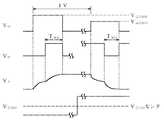
次に、本実施の形態の駆動方法について、図2を参照しながら説明する。図2は、図1に示されるPWM駆動方式の液晶表示装置の一つの画素電極に与えられる印加電圧VPの変化を示すタイミングチャートである。ある1垂直期間(1V)内に信号線に与えられるデータ信号VDが正極性基準レベルにあるときに、走査線に与えられるゲート信号VGがハイレベルVGONPになると、薄膜トランジスタはオンし印加電圧VPは正極性基準レベルのデータ信号VDにつられて上昇し、さらにデータ信号VDが正極性のアクティブレベルになると、表示階調に応じて決められたパルス幅の期間TWPだけ印加電圧VPはデータ信号VDにつられて上昇する。次に、ゲート信号VGがローレベルとなると薄膜トランジスタはオフし、このときのアクティブマトリクス動作のために設けられている周知の蓄積容量(図示省略)により、印加電圧VPを保持する。この1垂直期間内では、共通電極には振幅中心VCOMセンタで決まるローレベルが供給される。
【0035】
次の1垂直期間内に信号線に与えられるデータ信号VDが負極性基準レベルにあるときに、走査線に与えられるゲート信号VGが正極性のハイレベルVGONPより低い負極性のハイレベルVGONNになると、薄膜トランジスタはオンし印加電圧VPは負極性基準レベルのデータ信号VDにつられて下降し、さらにデータ信号VDが負極性のアクティブレベルになると、表示階調に応じて決められたパルス幅の期間TWNだけ印加電圧VPはデータ信号VDにつられてさらに下降する。次に、ゲート信号VGがローレベルとなると薄膜トランジスタはオフし、このときの印加電圧VPを保持する。この1垂直期間内では、共通電極には振幅中心VCOMセンタで決まるハイレベルが供給される。
【0036】
次に本発明の第2実施の形態について説明する。液晶への印加電圧は、薄膜トランジスタのオン電流とデータパルス幅の積に比例する。本実施の形態では、書き込みデータ極性によりデータパルス幅TWを補正し、その補正量をパネル温度により変えることを特徴としている。たとえば、正極性の書き込みデータのときのデータパルス幅TWPを負極性の書き込みデータのときのデータパルス幅TWNより広く、言いかえると負極性の書き込みデータのときのデータパルス幅TWNを正極性の書き込みデータのときのデータパルス幅TWPより狭く設定することにより、液晶への印加電圧を正極性データの書き込みと負極性データの書き込みとで書き込み量を等しくして、書き込み非対称性を低減したPWM駆動を実現できる。
【0037】
さらに、このような関係を維持しつつ、正極性の書き込みデータのときのデータパルス幅TWPと負極性の書き込みデータのときのデータパルス幅TWNともに、パネル温度の上昇にともない狭く設定することにより、パネル温度の変動によらず書き込み量を一定にすることができ、階調−輝度特性のずれを低減できる。この結果、パネル温度の変化によらず、液晶表示パネルの表示画質の変化を小さくすることができ、また、パネル温度の変化によらず、チラツキ及び焼き付きを小さくすることができる。よって、PWM駆動の特色である構成の簡単な階調電圧発生回路を用いながら、多階調表示を実現しつつ、上述した効果を得ることができる。
【0038】
次に本発明の第3実施の形態について説明する。図4は、本実施の形態の液晶表示装置の構成および駆動方法を説明するためのブロック図である。上述した第1実施の形態の温度検出回路7は、液晶表示パネルの外部に設けつつ、液晶表示パネルのパネル温度を検出することを想定したものであった。これに対し、本実施の形態では、液晶表示パネル1内に、パネル温度を検出する温度検出手段8を設けたことを特徴としている。
【0039】
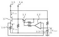
例えば、画素スイッチング用の薄膜トランジスタと同時にモニター用の薄膜トランジスタを形成し、モニター用の薄膜トランジスタのオン電流ION(又はこれに関連するパラメータ)を検出して、パネル温度によらず一定となるようにゲートオン電圧VGONを設定することを特徴とするものである。図5は、このような温度検出手段8の回路構成例を説明するための回路図である。ここで、電源は端子15より供給される。薄膜トランジスタ9はモニター用であり液晶表示パネル1の内部に設けられ、このモニター用薄膜トランジスタ9がオンしているときのオン電流で決まる電圧VONと基準電圧VREF(抵抗R13とツェナーダイオード13とで構成された基準電圧源が出力する)との差電圧を増幅して制御トランジスタ11を制御し、モニター用薄膜トランジスタ9のゲートにオン電流を一定にするようにフィードバックするとともに、補正信号として端子14に出力する。この補正信号は、DC/DCコンバータ4に出力される。また共通電圧中心VCOMセンタも温度補正を行う。
【0040】
本実施の形態では、モニター用の薄膜トランジスタを液晶表示パネル1に設けており、より液晶に近い箇所でパネル温度を検出できるので、第1実施の形態と比較してより精密な補正を実現できる。また、本実施の形態の温度検出手段8の薄膜トランジスタ以外の回路構成は、液晶表示パネルの外部に配置することも考えられるし、SOG(system on glass)技術を採用し画素スイッチング用の薄膜トランジスタと同時に液晶表示パネル内に形成することも考えられる。
【0041】
次に本発明の第4実施の形態について説明する。PWM駆動方式の液晶表示装置では、カウンタにより基準クロック信号を計数し、階調データとカウンタの出力とを比較して、表示階調に対応する書き込みデータのパルス幅TWを設定している。本実施の形態では、基準クロック信号の周波数をパネル温度により変えることを特徴としている。例えば、基準クロック信号の周波数を高くすることにより書き込みデータのパルス幅TWは狭くなり、周波数を低くすることにより書き込みデータのパルス幅TWは広くなるので、これを第2実施の形態で説明したようなパネル温度及び書き込みデータ極性によりデータパルス幅TWを補正するものに適用するのである。
【0042】
正極性の書き込みデータのときのデータパルス幅TWPを負極性の書き込みデータのときのデータパルス幅TWNよりも広く設定しておいて、パネル温度に応じて基準クロック信号の周波数を変えて書き込みデータのパルス幅TWを設定することで、パネル温度変化による階調−輝度特性のずれ及び書き込み非対称性を低減したPWM駆動を実現できる。
【0043】
また、画素スイッチング用薄膜トランジスタと同時形成されたモニター用薄膜トランジスタを用い、モニター用薄膜トランジスタのオン電流IONに比例するように基準クロック信号の周波数を設定することも考えられる。
【0044】
以上、好ましい実施の形態について説明したが、本発明は上述した実施の形態に限定されるものではなく、様々な変更や追加、上述した実施の形態同士の組合せが可能である。温度検出手段としては、サーミスタを用いることもできる。サーミスタを温度検出手段とした温度検出回路の例としては、特開平06-138843号公報の図2に示されるような電圧設定回路を中心とする構成も用いることができる。また、サーミスタではなく熱電対などの他の温度検出手段も採用可能であろう。
【0045】
上述した実施の形態では、液晶表示パネルの具体的な構成について言及してこなかったが、透過型液晶表示パネルを用いる場合は、上述した第3実施の形態のようにパネル上に温度検出手段を形成することができ、例えば、パネル内の表示領域の周りの周辺領域に形成するとよい。利用者からみて液晶表示パネルの背面側に配置されるバックライトユニットからの出射光の妨げにならないようにしつつ、高輝度の液晶表示を実現できる。
【0046】
反射型液晶表示パネルの場合には、第3実施の形態のようにパネル上に温度検出手段を形成することができ、また液晶表示パネルの背面側に配置することもできる。反射型液晶表示パネルの場合には、背面側に配置しても表示特性に影響を与えない。また、パネル内の周辺領域、場合によっては表示領域にも形成できる。反射型液晶表示パネルでは、表示領域に反射板を兼ねる画素電極がアレイ状に配列されており、各画素電極は画素スイッチング用の薄膜トランジスタの上方を覆っている。モニター用の薄膜トランジスタを、画素スイッチング用の薄膜トランジスタと同様に画素電極の下方に配置すれば、表示特性の悪化を招かずに表示領域に配置することもできる。
【0047】
半透過型液晶表示パネルの場合は、透過部及び反射部の画素電極のうち、反射部の画素電極の下方に温度検出手段を配置すれば、表示特性の悪化を招かずに表示領域に配置することができる。
【0048】
また、温度検出回路は、SOG技術だけでなく、COG(chip on glass)技術で形成してもよい。さらにまた、温度検出手段に液晶表示パネルの複数箇所のパネル温度を検出させることにより、パネル内の面内温度分布に応じた補正制御を行うことも可能であろう。
【0049】
また、液晶表示パネルの駆動方法は、図2で示した1垂直期間(1V)毎にデータ信号の極性を反転させるフレーム反転駆動であっても、1水平期間(1H)毎にデータ信号の極性を反転させ、さらに1垂直期間(1V)毎に極性を反転するゲート反転駆動であってもよい。
【0050】
【発明の効果】
本発明によれば、表示階調に応じたパルス幅期間だけデータ信号VDをアクティブレベルにするとともに、データ信号VDの極性に応じて、供給されるゲート信号VGのゲートオン電圧VGONPとゲートオン電圧VGONNとを異ならせ、またゲートオン電圧VGONPをゲートオン電圧VGONNより大きくしているので、薄膜トランジスタのオン電流IONを正極性と負極性とで等しくでき、書き込み非対称性を低減したPWM駆動を実現できる。
【0051】
さらに、このような関係を維持しつつ、パネル温度に応じて、図3(a)及び図3(b)に示される補正をゲートオン電圧及び共通電圧中心に対して行いつつ駆動することにより、パネル温度の変動によらず薄膜トランジスタのオン電流が一定となり階調−輝度特性のずれが低減できる。この結果、パネル温度の変化によらず、液晶表示パネルの表示画質の変化を小さくすることができる。また、パネル温度に応じて正極性ゲートオン電圧と負極性ゲートオン電圧との補正量を調整できるため、パネルの温度変化によるチラツキ及び焼き付きを抑制することができる。よって、PWM駆動の特色である構成の簡単な階調電圧発生回路を用いながら、多階調表示を実現しつつ、上述した効果を得ることができる。
【図面の簡単な説明】
【図1】本発明の第1実施の形態による液晶表示装置の構成および駆動方法を説明するためのブロック図である。
【図2】図1に示されるPWM駆動方式の液晶表示装置の一つの画素電極に与えられる印加電圧VPの変化を示すタイミングチャートである。
【図3】(a)パネル温度補正のためのパネル温度とゲートオン電圧との関係を示す特性図である。
(b)パネル温度補正のためのパネル温度と共通電圧中心(VCOMセンタ)との関係を示す特性図である。
【図4】本発明の第三の実施の形態による液晶表示装置の構成および駆動方法を説明するためのブロック図である。
【図5】本発明による温度検出手段8の回路構成例を説明するための回路図である。
【図6】従来の液晶表示装置の主要部分を示すブロック図である。
【図7】図6に示されるPWM駆動方式の液晶表示装置のある画素電極103に与えられる印加電圧VPの変化を示すタイミングチャートである。
【符号の説明】
1 液晶表示パネル
2 走査線駆動回路
3 信号線駆動回路
4 DC/DCコンバータ
5 スイッチ
6 コントローラ
7 温度検出回路
8 温度検出手段[0001]
BACKGROUND OF THE INVENTION
The present invention relates to a driving method of an active matrix liquid crystal display device, and more particularly to a driving method of a pulse width modulation driving type liquid crystal display device using a thin film transistor as a switching element and a liquid crystal display device driven by the driving method.
[0002]
[Prior art]
An active matrix liquid crystal display device that performs gradation display by a pulse width modulation (PWM) method is known. In the driving method of the liquid crystal display device by the PWM method, the voltage application period is not changed according to the display gradation, but the voltage application period is changed according to the display gradation. The display according to each gradation is realized. In the liquid crystal display device of the PWM drive system, the number of display gradations can be increased while using a gradation voltage generation circuit with a simple configuration.
[0003]
A method for driving such a liquid crystal display device of the PWM drive system will be described by taking the one proposed in Japanese Patent Laid-Open No. 04-142592 as an example. FIG. 6 is a block diagram showing main parts of a conventional liquid crystal display device. The conventional liquid crystal display device includes a plurality of
[0004]
FIG. 7 is a timing chart showing changes in the applied voltage VP applied to the
[0005]
In Japanese Patent Laid-Open No. 04-142592, in order to prevent the voltage applied to the pixel electrode from being asymmetrical with the data polarity for writing and causing flickering and burn-in, the gate-on voltage when the data signal is negative is set to VGONN , The gate-on voltage in the case of positive polarity is VGONP VGONN VGONP It has also been proposed to set it lower.
[0006]
[Problems to be solved by the invention]
By the way, about the liquid crystal display device of such a PWM drive system, the panel temperature and display characteristic of a liquid crystal display panel are examined. The on-current of the thin film transistor connected to the pixel electrode and performing a switching operation depends on the panel temperature, and increases as the panel temperature increases. Since the voltage applied to the liquid crystal is proportional to the product of the on-current and the data signal pulse width, the display gradation-luminance characteristics of the liquid crystal display panel change according to the panel temperature. Therefore, when the panel temperature changes, the display image quality of the liquid crystal display panel changes. Further, since the electrical characteristics of the thin film transistor depend on the panel temperature, the asymmetry of the writing amount depending on the data polarity varies depending on the panel temperature, and flickering and image sticking occur when the panel temperature changes.
[0007]
SUMMARY OF THE INVENTION Accordingly, an object of the present invention is to provide a method for driving a liquid crystal display device of a PWM system capable of suppressing changes in display gradation-luminance characteristics due to changes in panel temperature and burn-in of a liquid crystal display panel, and a liquid crystal display device driven by the driving method Is to provide.
[0008]
[Means for Solving the Problems]
According to the present invention, in a driving method of an active matrix type liquid crystal display device which is driven by a pulse width modulation method using a thin film transistor as a switching element, it has a panel temperature detecting means, and has a gate-on voltage or a data signal pulse width, a reference clock. A method for driving an active matrix liquid crystal display device, comprising: correcting a signal frequency according to a panel temperature; and correcting a gate-on voltage correction amount or a data signal pulse width correction amount according to a write data polarity according to a panel temperature; A liquid crystal display device driven by the driving method is obtained.
[0009]
A feature of the present invention is that a pulse width modulation driving type liquid crystal display device using a thin film transistor as a switching element and a driving method thereof correct the applied voltage to the liquid crystal in accordance with the write data polarity, and this correction is performed on the liquid crystal display. It is characterized by considering the panel temperature of the panel.
[0010]
One of the features is that the liquid crystal is driven while correcting the gate-on voltage in accordance with the relationship shown in the graph of FIG. That is, according to the control signal from the temperature detection circuit 7 of FIG. 1, the DC / DC converter 4 lowers the positive and negative gate-on voltages as the panel temperature is higher, and increases the positive and negative characteristics as the panel temperature is lower. Set the gate-on voltage high. The positive gate-on voltage is always set higher than the negative gate-on voltage.
[0011]
Further, as another feature, the common voltage center V is changed according to the relationship shown in the graph of FIG.COM The liquid crystal is driven while correcting the center. That is, according to the control signal from the temperature detection circuit 7 in FIG.COM The higher the center, the lower the panel temperature,COM Set the center low.
[0012]
By such liquid crystal driving, the data signal VD Is set to the active level only during the pulse width period corresponding to the display gradation, and the data signal VD Gate signal V supplied according to the polarity ofG The gate-on voltage of the positive gate-on voltage VGONP The negative gate on voltage VGONN Since it is larger, the on-current I of the thin film transistorON Can be made equal when writing positive polarity data and when writing negative polarity data, and PWM drive with reduced writing asymmetry can be realized.
[0013]
Further, while maintaining such a relationship, the panel is driven while performing the correction shown in FIGS. 3A and 3B with respect to the gate-on voltage and the common voltage center according to the panel temperature. The on-state current of the thin film transistor becomes constant regardless of temperature fluctuations, and a shift in display gradation-luminance characteristics can be reduced. Further, flickering and image sticking due to variations in panel temperature can be reduced. As a result, a change in display image quality of the liquid crystal display panel due to a change in panel temperature can be reduced.
[0014]
In particular, according to the present invention, a liquid crystal display panel having a plurality of switching thin film transistors (TFTs) respectively connected to a plurality of pixel electrodes is provided.Data signal In a driving method of an active matrix type liquid crystal display device (hereinafter simply referred to as an active matrix type liquid crystal display device) driven by a pulse width modulation driving method, the positive gate-on voltage (VGPONP) of the thin film transistorThe Negative polarity gate-on voltage (VGONN)Detected by a predetermined temperature detection means while maintaining this relationship. Panel temperature of the liquid crystal display panelAs the panel temperature rises, both the positive gate-on voltage (VGONP) and the negative gate-on voltage (VGONN) are lower than before the panel temperature rises. A driving method of a liquid crystal display device characterized by setting is obtained.
[0015]
Preferably, the center (V) of the common voltage supplied to the common electrode of the liquid crystal display panel.COM The center) is also set based on the panel temperature.
[0017]
Further, in the driving method of an active matrix type liquid crystal display device in which a liquid crystal display panel including a plurality of switching thin film transistors respectively connected to a plurality of pixel electrodes is driven by a pulse width modulation driving method of a data signal, the switching thin film transistor ON current (I0N) isDetected by a predetermined temperature detecting means SaidLCD display panel To be constant regardless of panel temperatureUsing a given circuit Positive gate-on voltage (VGPONP) of the switching thin film transistor) And negative gate-on voltage (VGONN)The positive polarity data pulse width (TWP) of the data signal in all display gradations is longer than the negative polarity data pulse width (TWN). A driving method of a liquid crystal display device, which is also characterized by setting, can be obtained.
[0018]
Further, the liquid crystal display panel is provided with the switching thin film transistor.On the LCD panel Thin film transistor for monitor formedUsing The on-current (I0N) of the switching thin film transistor is, SaidLCD display panel The positive gate-on voltage (VGONP) and negative gate-on voltage (VGONN) of the switching thin film transistor are set to be constant regardless of the panel temperature.The positive polarity data pulse width (TWP) of the data signal in all display gradations is set longer than the negative polarity data pulse width (TWN). A driving method of a liquid crystal display device characterized by this can also be obtained.
[0019]
According to the present invention, in the driving method of the active matrix type liquid crystal display device, the positive data pulse width (TWP) of the data signal in all display gradations is longer than the negative data pulse width (TWN). Set,The liquid crystal display panel detected by the predetermined temperature detection means As the panel temperature rises, a method of driving a liquid crystal display device is obtained, in which the positive gate-on voltage (VGONP) and the negative gate-on voltage (VGONN) of the thin film transistor are set low.
[0021]
In the above driving method, the positive data pulse width (TWP) of the data signal in all display gradations is set longer than the negative data pulse width (TWN), and this relationship is maintained.Detected by predetermined temperature detection means A liquid crystal display device characterized in that both the positive data pulse width (TWP) and the negative data pulse width (TWN) are made shorter than before the panel temperature rises due to a rise in the panel temperature of the liquid crystal display panel. This driving method is also obtained.
[0022]
Furthermore, according to the present invention, in the above driving method,The positive polarity data pulse width (TWP) of the data signal is set longer than the negative polarity data pulse width (TWN), while maintaining this relationship, Each display gradation is given by the number of clocks, the reference clock signal is counted by a counter, the gradation data and the output of the counter are compared, the pulse width (TW) of the data signal is set, and the frequency of the reference clock signal TheDetected by a predetermined temperature detecting means The panel temperature of the liquid crystal display panelBased on this, a method for driving a liquid crystal display device can be obtained in which the frequency of the reference clock is increased when the panel temperature rises. OrThe positive polarity data pulse width (TWP) of the data signal is set longer than the negative polarity data pulse width (TWN), while maintaining this relationship, A method of driving a liquid crystal display device, comprising: using a thin film transistor for monitoring simultaneously formed with the thin film transistor for switching, and setting a frequency of the reference clock signal so as to be proportional to an on-current (ION) of the thin film transistor for monitoring Can also be obtained. At this time, it is desirable that the positive gate on voltage (VGONP) is set higher than the negative gate on voltage (VGONN).
[0023]
In the present invention, the positive data pulse width (T) of the data signal in all display gradations.WP ) For the negative polarity data pulse width (TWN It is desirable to set longer than
[0024]
Further, according to the present invention, the center of the common voltage (V) supplied to the common electrode of the liquid crystal display panel as the panel temperature rises.COM It is preferable to increase the center.
[0025]
Further, according to the present invention, a liquid crystal display device driven by each of the above driving methods can be obtained.
[0026]
DETAILED DESCRIPTION OF THE INVENTION
Next, embodiments of the present invention will be described in detail with reference to the drawings. FIG. 1 is a block diagram for explaining a configuration and a driving method of the liquid crystal display device according to the first embodiment. The liquid crystal display device of the present embodiment includes a liquid
[0027]
Although not shown, the liquid
[0028]
The DC / DC converter 4 generates and outputs various voltages necessary for liquid crystal driving of the liquid
[0029]
The
[0030]
The controller 6 receives an input signal from an external device, that is, an image signal and a control signal such as a horizontal synchronizing signal and a vertical synchronizing signal, and performs scanning
[0031]
The temperature detection circuit 7 detects the panel temperature of the liquid
[0032]
The voltage applied to the liquid crystal is proportional to the product of the on-current of the thin film transistor and the data pulse width. Further, there is a simple increase correlation between the gate-on voltage and the on-current of the thin film transistor. In the present embodiment, liquid crystal driving is performed while correcting the gate-on voltage in accordance with the relationship shown in the graph of gate-on voltage-panel temperature correction in FIG. That is, according to the control signal S4 from the temperature detection circuit 7, the DC / DC converter 4 lowers the positive and negative gate-on voltages as the panel temperature is higher, and the positive and negative gate-on voltages as the panel temperature is lower. Set high. The positive gate-on voltage is always set higher than the negative gate-on voltage.
[0033]
Further, in the present embodiment, V in FIG.COM In accordance with the relationship shown in the center-panel temperature correction graph, the common voltage center (VCOM The liquid crystal is driven while correcting the center. That is, according to the control signal S4 from the temperature detection circuit 7, the DC / DC converter 4 causes V to increase as the panel temperature increases.COM The higher the center, the lower the panel temperature,COM Set the center low.
[0034]
Next, the driving method of the present embodiment will be described with reference to FIG. FIG. 2 shows an applied voltage V applied to one pixel electrode of the liquid crystal display device of the PWM drive type shown in FIG.P It is a timing chart which shows the change of. Data signal V applied to the signal line within a certain vertical period (1V)D Is at the positive reference level, the gate signal V applied to the scan lineG Is high level VGONP The thin film transistor turns on and the applied voltage VP Is the positive polarity reference level data signal VD And then the data signal VD Becomes a positive active level, the pulse width period T determined according to the display gradationWP Applied voltage V onlyP Is the data signal VD Ascended to rise. Next, the gate signal VG Is turned to a low level, the thin film transistor is turned off, and the applied voltage V is applied by a well-known storage capacitor (not shown) provided for the active matrix operation at this time.P Hold. Within this one vertical period, the common electrode has an amplitude center VCOM A low level determined by the center is supplied.
[0035]
Data signal V applied to the signal line within the next one vertical periodD Is at the negative reference level, the gate signal V applied to the scanning lineG Is positive high level VGONP Lower negative high level VGONN The thin film transistor turns on and the applied voltage VP Is the negative reference level data signal VD The data signal VD Becomes a negative active level, a period T of a pulse width determined according to the display gradationWN Applied voltage V onlyP Is the data signal VD Then, it goes down further. Next, the gate signal VG Becomes low level, the thin film transistor is turned off, and the applied voltage VP Hold. Within this one vertical period, the common electrode has an amplitude center VCOM A high level determined by the center is supplied.
[0036]
Next, a second embodiment of the present invention will be described. The voltage applied to the liquid crystal is proportional to the product of the on-current of the thin film transistor and the data pulse width. In the present embodiment, the data pulse width T depends on the write data polarity.W And the amount of correction varies depending on the panel temperature. For example, the data pulse width T for positive write dataWP Is the data pulse width T when the negative write dataWN More broadly, in other words, the data pulse width T for negative write dataWN Is the data pulse width T for positive polarity write dataWP By setting the voltage more narrowly, it is possible to realize the PWM drive in which the writing voltage is equalized between the writing of the positive polarity data and the writing of the negative polarity data, and the writing asymmetry is reduced.
[0037]
Further, while maintaining such a relationship, the data pulse width T in the case of positive polarity write dataWP And data pulse width T for negative polarity write dataWN In both cases, the setting is made narrower as the panel temperature rises, so that the amount of writing can be made constant regardless of variations in the panel temperature, and the deviation of the gradation-luminance characteristics can be reduced. As a result, the change in the display image quality of the liquid crystal display panel can be reduced regardless of the change in the panel temperature, and the flicker and burn-in can be reduced regardless of the change in the panel temperature. Therefore, the above-described effect can be obtained while realizing multi-gradation display using a simple gradation voltage generation circuit having a configuration that is a feature of PWM driving.
[0038]
Next, a third embodiment of the present invention will be described. FIG. 4 is a block diagram for explaining a configuration and a driving method of the liquid crystal display device of the present embodiment. The temperature detection circuit 7 of the first embodiment described above is assumed to detect the panel temperature of the liquid crystal display panel while being provided outside the liquid crystal display panel. On the other hand, the present embodiment is characterized in that a temperature detecting means 8 for detecting the panel temperature is provided in the liquid
[0039]
For example, a thin film transistor for monitoring is formed simultaneously with a thin film transistor for pixel switching, and an on-current I of the thin film transistor for monitoring is formed.ON (Or related parameters) is detected and the gate-on voltage V is set so as to be constant regardless of the panel temperature.GON Is set. FIG. 5 is a circuit diagram for explaining an example of the circuit configuration of such temperature detecting means 8. Here, the power is supplied from the terminal 15. The thin film transistor 9 is for monitoring and is provided inside the liquid
[0040]
In the present embodiment, a thin film transistor for monitoring is provided in the liquid
[0041]
Next, a fourth embodiment of the present invention will be described. In the liquid crystal display device of the PWM drive system, the reference clock signal is counted by a counter, the gradation data is compared with the output of the counter, and the pulse width T of the write data corresponding to the display gradation is obtained.W Is set. This embodiment is characterized in that the frequency of the reference clock signal is changed according to the panel temperature. For example, by increasing the frequency of the reference clock signal, the write data pulse width TW Becomes narrower, and the pulse width T of the write data is reduced by lowering the frequency.W Therefore, the data pulse width T depends on the panel temperature and the write data polarity as described in the second embodiment.W It applies to the one that corrects.
[0042]
Data pulse width T for positive write dataWP Is the data pulse width T when the negative write dataWN The width of the write data is changed by changing the frequency of the reference clock signal according to the panel temperature.W By setting, PWM driving with reduced gradation-luminance characteristic shift and writing asymmetry due to panel temperature change can be realized.
[0043]
Also, a monitor thin film transistor formed simultaneously with the pixel switching thin film transistor is used.ON It is also conceivable to set the frequency of the reference clock signal so as to be proportional to.
[0044]
As mentioned above, although preferable embodiment was described, this invention is not limited to embodiment mentioned above, A various change and addition and the combination of embodiment mentioned above are possible. A thermistor can also be used as the temperature detecting means. As an example of a temperature detection circuit using a thermistor as temperature detection means, a configuration centering on a voltage setting circuit as shown in FIG. 2 of Japanese Patent Laid-Open No. 06-138843 can be used. Also, other temperature detection means such as a thermocouple may be employed instead of the thermistor.
[0045]
In the above-described embodiment, the specific configuration of the liquid crystal display panel has not been mentioned. However, when a transmissive liquid crystal display panel is used, a temperature detecting means is provided on the panel as in the above-described third embodiment. For example, it may be formed in a peripheral region around the display region in the panel. A high-brightness liquid crystal display can be realized while preventing the light emitted from the backlight unit disposed on the back side of the liquid crystal display panel from being viewed by the user.
[0046]
In the case of a reflective liquid crystal display panel, temperature detecting means can be formed on the panel as in the third embodiment, and can also be arranged on the back side of the liquid crystal display panel. In the case of a reflective liquid crystal display panel, even if it is arranged on the back side, the display characteristics are not affected. It can also be formed in a peripheral area in the panel, and in some cases in a display area. In a reflective liquid crystal display panel, pixel electrodes that also serve as reflectors are arranged in an array in a display area, and each pixel electrode covers a thin film transistor for pixel switching. If the monitor thin film transistor is disposed below the pixel electrode in the same manner as the pixel switching thin film transistor, the display thin film transistor can be disposed in the display region without deteriorating display characteristics.
[0047]
In the case of a transflective liquid crystal display panel, if the temperature detecting means is arranged below the pixel electrode of the reflective part among the pixel electrodes of the transmissive part and the reflective part, it is arranged in the display region without causing deterioration of display characteristics. be able to.
[0048]
The temperature detection circuit may be formed not only by the SOG technique but also by a COG (chip on glass) technique. Furthermore, it is also possible to perform correction control according to the in-plane temperature distribution in the panel by causing the temperature detecting means to detect the panel temperature at a plurality of positions of the liquid crystal display panel.
[0049]
Further, even if the liquid crystal display panel is driven by frame inversion driving in which the polarity of the data signal is inverted every one vertical period (1V) shown in FIG. 2, the polarity of the data signal every horizontal period (1H). Inversion driving may be performed, and the polarity is inverted every vertical period (1 V).
[0050]
【The invention's effect】
According to the present invention, the data signal V is applied only during the pulse width period corresponding to the display gradation.D And the gate signal V to be supplied in accordance with the polarity of the data signal VD.G Gate-on voltage VGONP And gate-on voltage VGONN And the gate-on voltage VGONP The gate-on voltage VGONN Since it is larger, the on-current I of the thin film transistorON Can be made equal for positive polarity and negative polarity, and PWM drive with reduced write asymmetry can be realized.
[0051]
Further, while maintaining such a relationship, the panel is driven while performing the correction shown in FIGS. 3A and 3B with respect to the gate-on voltage and the common voltage center according to the panel temperature. The on-state current of the thin film transistor becomes constant regardless of temperature fluctuations, and the shift in gradation-luminance characteristics can be reduced. As a result, the change in the display image quality of the liquid crystal display panel can be reduced regardless of the change in the panel temperature. Further, since the correction amount between the positive gate-on voltage and the negative gate-on voltage can be adjusted according to the panel temperature, flicker and burn-in due to panel temperature change can be suppressed. Therefore, the above-described effects can be obtained while realizing multi-gradation display using a simple gradation voltage generation circuit having a configuration that is a characteristic of PWM driving.
[Brief description of the drawings]
FIG. 1 is a block diagram for explaining a configuration and a driving method of a liquid crystal display device according to a first embodiment of the present invention.
FIG. 2 is a timing chart showing a change in applied voltage VP applied to one pixel electrode of the PWM drive type liquid crystal display device shown in FIG. 1;
FIG. 3A is a characteristic diagram showing a relationship between a panel temperature for correcting the panel temperature and a gate-on voltage.
(B) Panel temperature and common voltage center (VCOM It is a characteristic view showing the relationship with the center.
FIG. 4 is a block diagram for explaining a configuration and a driving method of a liquid crystal display device according to a third embodiment of the present invention.
FIG. 5 is a circuit diagram for explaining a circuit configuration example of temperature detecting means 8 according to the present invention.
FIG. 6 is a block diagram showing main parts of a conventional liquid crystal display device.
7 is an applied voltage V applied to a
[Explanation of symbols]
1 LCD panel
2 Scanning line drive circuit
3 Signal line drive circuit
4 DC / DC converter
5 switch
6 Controller
7 Temperature detection circuit
8 Temperature detection means
Claims (11)
Translated fromJapanese前記薄膜トランジスタの正極性ゲートオン電圧(VGONP)を負極性ゲートオン電圧(VGONN)よりも高く設定し、
この関係を維持しつつ、所定の温度検出手段により検出した前記液晶表示パネルのパネル温度の上昇にともない前記正極性ゲートオン電圧(VGONP)および前記負極性ゲートオン電圧(VGONN)の両方を前記パネル温度の上昇前よりも低く設定することを特徴とする液晶表示装置の駆動方法。In a driving method of an active matrix type liquid crystal display device for driving a liquid crystal display panel including a plurality of switching thin film transistors respectively connected to a plurality of pixel electrodes bya pulse width modulation driving method of adata signal ,
A positive gate on voltage (VGONP)of the thin film transistor isset higher than a negative gate on voltage (VGONN);
While maintaining this relationship, both thepositive gate-on voltage (VGONP) and the negative gate-on voltage (VGONN) aredetected at the panel temperatureas the panel temperatureof the liquid crystal display paneldetected by a predetermined temperature detectorincreases. A driving method of a liquid crystal display device, characterized in that it is setlower than before the rise .
前記スイッチング用薄膜トランジスタのオン電流(I0N)が、所定の温度検出手段により検出した前記液晶表示パネルのパネル温度によらず一定となるように、所定の回路を用いて前記スイッチング用薄膜トランジスタの正極性ゲートオン電圧(VGONP)および負極性ゲートオン電圧(VGONN)を設定し、
全表示階調における前記データ信号の正極性データパルス幅(TWP)を負極性データパルス幅(TWN)よりも長く設定することを特徴とする液晶表示装置の駆動方法。In a driving method of an active matrix type liquid crystal display device for driving a liquid crystal display panel including a plurality of switching thin film transistors respectively connected to a plurality of pixel electrodes by a pulse width modulation driving method of a data signal,
A positive gate on of the thin film transistor for switching is turned onusing a predetermined circuit so that an ON current (I0N) of the thin film transistor for switching becomes constant regardlessof a panel temperature of theliquid crystal display paneldetected by a predetermined temperature detecting means. Set the voltage (VGPONP) and negative gate-on voltage (VGONN),
A driving method of a liquid crystal display device,wherein a positive data pulse width (TWP) of the data signal in all display gradations is setlonger than a negative data pulse width (TWN) .
前記スイッチング用薄膜トランジスタと同時に前記液晶表示パネルに形成されたモニター用薄膜トランジスタを用いて、前記スイッチング用薄膜トランジスタのオン電流(I0N)が、前記液晶表示パネルのパネル温度によらず一定となるように前記スイッチング用薄膜トランジスタの正極性ゲートオン電圧(VGONP)および負極性ゲートオン電圧(VGONN)を設定し、
全表示階調における前記データ信号の正極性データパルス幅(TWP)を前記負極性データパルス幅(TWN)よりも長く設定することを特徴とする液晶表示装置の駆動方法。In a driving method of an active matrix type liquid crystal display device for driving a liquid crystal display panel including a plurality of switching thin film transistors respectively connected to a plurality of pixel electrodes by a pulse width modulation driving method of a data signal,
Usingtheliquid crystal display monitor thin film transistors formedon the panel to the switching thin film transistor and simultaneously, the on-current of the switching thin film transistor (i0n) issaid to be constant irrespective of the panel temperatureof theliquid crystal display panel Set the positive gate-on voltage (VGPONP) and negative gate-on voltage (VGONN) of the switching thin film transistor,
A driving method of a liquid crystal display device, characterized in thata positive data pulse width (TWP) of the data signal in all display gradations is set longer than the negative data pulse width (TWN) .
全表示階調における前記データ信号の正極性データパルス幅(TWP)を負極性データパルス幅(TWN)よりも長く設定し、
所定の温度検出手段により検出した前記液晶表示パネルのパネル温度の上昇にともない前記薄膜トランジスタの正極性ゲートオン電圧(VGONP)および負極性ゲートオン電圧(VGONN)を低く設定することを特徴とする液晶表示装置の駆動方法。In a driving method of an active matrix type liquid crystal display device for driving a liquid crystal display panel including a plurality of switching thin film transistors respectively connected to a plurality of pixel electrodes by a pulse width modulation driving method of a data signal,
The positive polarity data pulse width (TWP) of the data signal in all display gradations is set longer than the negative polarity data pulse width (TWN),
A liquid crystal display device characterized in that a positive gate on voltage (VGONP) and a negative gate on voltage (VGONN) of the thin film transistor are set low asthe panel temperature of theliquid crystal display panel detected by a predetermined temperature detecting means rises. Driving method.
全表示階調における前記データ信号の正極性データパルス幅(TWP)を負極性データパルス幅(TWN)よりも長く設定し、
この関係を維持しつつ、所定の温度検出手段により検出した前記液晶表示パネルのパネル温度の上昇により前記正極性データパルス幅(TWP)および前記負極性データパルス幅(TWN)の両方を前記パネル温度の上昇前よりも短くすることを特徴とする液晶表示装置の駆動方法。In a driving method of an active matrix type liquid crystal display device for driving a liquid crystal display panel including a plurality of switching thin film transistors respectively connected to a plurality of pixel electrodes by a pulse width modulation driving method of a data signal,
The positive polarity data pulse width (TWP) of the data signal in all display gradations is set longer than the negative polarity data pulse width (TWN),
While maintaining this relationship, both the positive data pulse width (TWP) and the negative data pulse width (TWN) are set to the panel temperature as the panel temperature of the liquid crystal display paneldetected by a predetermined temperature detecting means increases. A method for driving a liquid crystal display device, characterized in that the driving time is shorter than before the rise.
全表示階調における前記データ信号の正極性データパルス幅(TWP)を負極性データパルス幅(TWN)よりも長く設定し、
この関係を維持しつつ、各表示階調をクロック数で与え、カウンタにより基準クロック信号を計数し、階調データとカウンタの出力とを比較して前記データ信号のパルス幅(TW)を設定するとともに、
前記基準クロック信号の周波数を、所定の温度検出手段により検出した前記液晶表示パネルのパネル温度に基づき、前記パネル温度が上昇したとき前記基準クロックの周波数を高くすることを特徴とする液晶表示装置の駆動方法。In a driving method of an active matrix type liquid crystal display device for driving a liquid crystal display panel including a plurality of switching thin film transistors respectively connected to a plurality of pixel electrodes by a pulse width modulation driving method of a data signal,
Set to be longer thanthe positive data pulse width (TWP) a negative datapathpulse widthof the data signal in more gradations(TWN),
While maintaining this relationship, each display gradation is given by the number of clocks, the reference clock signal is counted by the counter, and the pulse width (TW) of the data signal is set by comparing the gradation data with the output of the counter. With
The liquid crystal display device the frequency of the reference clocksignal,based on the panel temperature of the liquid crystal display paneldetected by a predetermined temperaturedetector,the panel temperature is characterized byhigh to Rukotothe frequency of the reference clock when elevated Driving method.
全表示階調における前記データ信号の正極性データパルス幅(TWP)を前記負極性データパルス幅(TWN)よりも長く設定し、
この関係を維持しつつ、各表示階調をクロック数で与え、カウンタにより基準クロック信号を計数し、階調データとカウンタの出力とを比較して前記データ信号のパルス幅(TW)を設定するとともに、
前記スイッチング用薄膜トランジスタと同時形成されたモニター用薄膜トランジスタを用い、前記モニター用薄膜トランジスタのオン電流(ION)に比例するように前記基準クロック信号の周波数を設定することを特徴とする液晶表示装置の駆動方法。In a driving method of an active matrix type liquid crystal display device for driving a liquid crystal display panel including a plurality of switching thin film transistors respectively connected to a plurality of pixel electrodes by a pulse width modulation driving method of a data signal,
A positive data pulse width (TWP) of the data signal in all display gradations is set to be longer than the negative data pulse width (TWN);
While maintaining this relationship, each display gradation is given by the number of clocks, the reference clock signal is counted by the counter, and the pulse width (TW) of the data signal is set by comparing the gradation data with the output of the counter. With
A method for driving a liquid crystal display device, comprising: using a thin film transistor for monitoring simultaneously formed with the thin film transistor for switching; and setting a frequency of the reference clock signal to be proportional to an on-current (ION) of the thin film transistor for monitoring .
Priority Applications (6)
| Application Number | Priority Date | Filing Date | Title |
|---|---|---|---|
| JP2002057274AJP3990167B2 (en) | 2002-03-04 | 2002-03-04 | Liquid crystal display device driving method and liquid crystal display device using the driving method |
| TW092104360ATW583635B (en) | 2002-03-04 | 2003-02-27 | Method of driving liquid crystal display and liquid crystal display using the driving method |
| KR10-2003-0013080AKR100519894B1 (en) | 2002-03-04 | 2003-03-03 | Method of driving liquid crystal display and liquid crystal display using the driving method |
| CNB03105112XACN1294546C (en) | 2002-03-04 | 2003-03-04 | Method for driving liquid crystal display and liquid crystal display using the driving method |
| US10/377,876US7071929B2 (en) | 2002-03-04 | 2003-03-04 | Method of driving liquid crystal display and liquid crystal display using the driving method |
| CNB2006100751400ACN100464216C (en) | 2002-03-04 | 2003-03-04 | Method for driving liquid crystal display and liquid crystal display using the driving method |
Applications Claiming Priority (1)
| Application Number | Priority Date | Filing Date | Title |
|---|---|---|---|
| JP2002057274AJP3990167B2 (en) | 2002-03-04 | 2002-03-04 | Liquid crystal display device driving method and liquid crystal display device using the driving method |
Publications (2)
| Publication Number | Publication Date |
|---|---|
| JP2003255304A JP2003255304A (en) | 2003-09-10 |
| JP3990167B2true JP3990167B2 (en) | 2007-10-10 |
Family
ID=27800114
Family Applications (1)
| Application Number | Title | Priority Date | Filing Date |
|---|---|---|---|
| JP2002057274AExpired - LifetimeJP3990167B2 (en) | 2002-03-04 | 2002-03-04 | Liquid crystal display device driving method and liquid crystal display device using the driving method |
Country Status (5)
| Country | Link |
|---|---|
| US (1) | US7071929B2 (en) |
| JP (1) | JP3990167B2 (en) |
| KR (1) | KR100519894B1 (en) |
| CN (2) | CN1294546C (en) |
| TW (1) | TW583635B (en) |
Families Citing this family (46)
| Publication number | Priority date | Publication date | Assignee | Title |
|---|---|---|---|---|
| JP3870954B2 (en) | 2003-07-31 | 2007-01-24 | セイコーエプソン株式会社 | Liquid crystal panel driving method, liquid crystal device and electronic apparatus |
| US7643020B2 (en)* | 2003-09-30 | 2010-01-05 | Intel Corporation | Driving liquid crystal materials using low voltages |
| FR2860607B1 (en)* | 2003-10-07 | 2006-02-24 | Thales Sa | LIQUID CRYSTAL CELL WITH INTEGRATED THERMAL SENSORS |
| GB0402046D0 (en)* | 2004-01-29 | 2004-03-03 | Koninkl Philips Electronics Nv | Active matrix display device |
| JP4528775B2 (en)* | 2004-02-20 | 2010-08-18 | 東芝モバイルディスプレイ株式会社 | Liquid crystal display |
| CN100458906C (en) | 2004-02-20 | 2009-02-04 | 三星电子株式会社 | Pulse compensator, display device and method of driving the display device |
| KR101056374B1 (en)* | 2004-02-20 | 2011-08-11 | 삼성전자주식회사 | Pulse compensator, image display device having same, and driving method of image display device |
| JP4674790B2 (en)* | 2004-03-31 | 2011-04-20 | シャープ株式会社 | Display device and electronic information device |
| US20060007207A1 (en)* | 2004-04-01 | 2006-01-12 | Toshiba Matsushita Display Technology Co., Ltd. | Liquid crystal display device and method of driving liquid crystal display device |
| KR101021202B1 (en)* | 2004-04-16 | 2011-03-11 | 엘지디스플레이 주식회사 | FCS mode liquid crystal display device having low temperature compensation circuit and its driving method |
| JP2005345974A (en)* | 2004-06-07 | 2005-12-15 | Toshiba Matsushita Display Technology Co Ltd | Liquid crystal display |
| JP4462036B2 (en)* | 2005-01-06 | 2010-05-12 | 株式会社デンソー | Liquid crystal display |
| JP4661412B2 (en)* | 2005-07-11 | 2011-03-30 | 三菱電機株式会社 | Method for driving liquid crystal panel and liquid crystal display device |
| KR20070008872A (en)* | 2005-07-12 | 2007-01-18 | 삼성전자주식회사 | Driving circuit of display device and display device including same |
| DE102006032262A1 (en)* | 2005-07-15 | 2007-05-03 | Samsung Electronics Co., Ltd., Suwon | A temperature sensor for a display device, a thin film transistor array panel including the temperature sensor, a liquid crystal display, a liquid crystal display drive circuit, and a liquid crystal display flicker control system |
| KR101197050B1 (en)* | 2005-07-26 | 2012-11-06 | 삼성디스플레이 주식회사 | Driving apparatus for display device and display device including the same |
| US20070024553A1 (en)* | 2005-07-28 | 2007-02-01 | Shigesumi Araki | Liquid crystal display device, display control method and display control apparatus |
| JP2007072162A (en)* | 2005-09-07 | 2007-03-22 | Mitsubishi Electric Corp | Display device |
| KR20070042367A (en)* | 2005-10-18 | 2007-04-23 | 삼성전자주식회사 | Drive voltage generation circuit compensated for the temperature, the liquid crystal display including the same, and a drive voltage generation method |
| KR101193111B1 (en)* | 2005-10-18 | 2012-10-22 | 삼성디스플레이 주식회사 | Circuit for generating temperature compensated driving voltage and liquid crystal display device having the same and method for generating driving voltage |
| CN101009076B (en)* | 2006-01-27 | 2010-05-12 | 奇美电子股份有限公司 | Plane display and display driving method |
| FR2897446A1 (en)* | 2006-02-15 | 2007-08-17 | Thomson Licensing Sas | LIQUID CRYSTAL DISPLAY DEVICE |
| KR101385229B1 (en)* | 2006-07-13 | 2014-04-14 | 삼성디스플레이 주식회사 | Gate on voltage generator, driving device and display apparatus comprising the same |
| TW200807369A (en)* | 2006-07-28 | 2008-02-01 | Innolux Display Corp | Driving system of liquid crystal display device |
| KR101328387B1 (en)* | 2006-08-25 | 2013-11-13 | 삼성디스플레이 주식회사 | Method of touch position detecting |
| KR101282189B1 (en)* | 2006-09-13 | 2013-07-05 | 삼성디스플레이 주식회사 | Voltage generating circuit and display apparatus having the same |
| KR20080033771A (en)* | 2006-10-13 | 2008-04-17 | 삼성전자주식회사 | Driving device of backlight unit, liquid crystal display device having same, and control method thereof |
| CN100449605C (en)* | 2006-11-07 | 2009-01-07 | 友达光电股份有限公司 | Driving system and driving method of color sequential liquid crystal display |
| JP2008292865A (en)* | 2007-05-25 | 2008-12-04 | Sony Corp | Cathode potential control device, self-luminous display device, electronic equipment, and cathode potential control method |
| KR100920376B1 (en)* | 2007-12-21 | 2009-10-07 | 엘지디스플레이 주식회사 | LCD and its driving method |
| KR101319339B1 (en)* | 2008-05-09 | 2013-10-16 | 엘지디스플레이 주식회사 | Driving circuit for liquid crystal display device and method for driving the same |
| JP5233847B2 (en) | 2009-06-03 | 2013-07-10 | 三菱電機株式会社 | Driving method of liquid crystal panel |
| TWI423240B (en)* | 2010-10-27 | 2014-01-11 | Au Optronics Corp | Method for controlling gate signals and device thereof |
| TWI453722B (en)* | 2011-04-12 | 2014-09-21 | Au Optronics Corp | Scan-line driving apparatus of liquid crystal display |
| TWI478142B (en)* | 2012-11-01 | 2015-03-21 | Au Optronics Corp | Flat displayer and driving module, circuit, and method for controlling voltage thereof |
| KR102071939B1 (en)* | 2013-05-23 | 2020-02-03 | 삼성디스플레이 주식회사 | Display appratus |
| KR102278875B1 (en)* | 2015-01-14 | 2021-07-20 | 삼성디스플레이 주식회사 | Gate driving circuit and display device having the same |
| CN104882106B (en)* | 2015-06-02 | 2017-05-31 | 武汉华星光电技术有限公司 | The liquid crystal display panel and its driving method of row inverted pattern |
| WO2017077651A1 (en)* | 2015-11-06 | 2017-05-11 | 堺ディスプレイプロダクト株式会社 | Display apparatus and voltage adjustment method |
| CN106952622A (en)* | 2016-01-06 | 2017-07-14 | 大陆汽车电子(芜湖)有限公司 | Instrument display screen contrast adjustment method based on feedback |
| KR102534116B1 (en)* | 2017-12-21 | 2023-05-19 | 삼성디스플레이 주식회사 | Dc to dc converter and display apparatus having the same |
| KR102783415B1 (en)* | 2020-03-11 | 2025-03-20 | 삼성디스플레이 주식회사 | Display apparatus and method of driving the same |
| US11961473B2 (en)* | 2020-11-27 | 2024-04-16 | Sharp Kabushiki Kaisha | Display device |
| KR102743795B1 (en)* | 2021-02-19 | 2024-12-18 | 가부시키가이샤 재팬 디스프레이 | radio reflector |
| CN115985221B (en)* | 2023-03-21 | 2023-07-21 | 深圳通锐微电子技术有限公司 | Source driver, bandwidth adjusting method and display panel |
| CN117198239A (en)* | 2023-08-31 | 2023-12-08 | 长沙惠科光电有限公司 | Display device driving method and display device |
Family Cites Families (15)
| Publication number | Priority date | Publication date | Assignee | Title |
|---|---|---|---|---|
| ATE135496T1 (en)* | 1990-03-27 | 1996-03-15 | Canon Kk | THIN FILM SEMICONDUCTOR COMPONENT |
| JP2941987B2 (en)* | 1990-04-09 | 1999-08-30 | キヤノン株式会社 | Liquid crystal display device and driving method thereof |
| JPH04142592A (en)* | 1990-10-04 | 1992-05-15 | Oki Electric Ind Co Ltd | Liquid crystal display device |
| JPH06347753A (en)* | 1993-04-30 | 1994-12-22 | Prime View Hk Ltd | Method and equipment to recover threshold voltage of amorphous silicon thin-film transistor device |
| JPH08211368A (en)* | 1995-02-07 | 1996-08-20 | Toshiba Corp | Liquid crystal display device and liquid crystal display device |
| GB9704149D0 (en)* | 1996-08-16 | 1997-04-16 | Philips Electronics Nv | Active matrix display devices and methods of driving such |
| JPH10268265A (en)* | 1997-03-25 | 1998-10-09 | Sharp Corp | Liquid crystal display |
| JP2000009547A (en)* | 1998-06-22 | 2000-01-14 | Hitachi Ltd | Temperature sensor, liquid crystal display device using the same, and projection type liquid crystal display device |
| JP3744714B2 (en)* | 1998-12-08 | 2006-02-15 | シャープ株式会社 | Liquid crystal display device and driving method thereof |
| JP2000258752A (en)* | 1999-03-09 | 2000-09-22 | Sharp Corp | Liquid crystal display |
| JP2000338518A (en) | 1999-06-01 | 2000-12-08 | Nec Corp | Liquid crystal display device, and manufacturing method of liquid crystal display device |
| JP3832162B2 (en)* | 1999-12-02 | 2006-10-11 | セイコーエプソン株式会社 | Liquid crystal panel driving method, liquid crystal device and electronic apparatus |
| KR100683519B1 (en)* | 1999-12-23 | 2007-02-15 | 엘지.필립스 엘시디 주식회사 | Charge characteristic compensation circuit and charge characteristic compensation method of liquid crystal panel |
| EP1180714A4 (en)* | 2000-03-27 | 2002-10-02 | Citizen Watch Co Ltd | Liquid crystal shutter |
| TW573290B (en) | 2000-04-10 | 2004-01-21 | Sharp Kk | Driving method of image display apparatus, driving apparatus of image display apparatus, and image display apparatus |
- 2002
- 2002-03-04JPJP2002057274Apatent/JP3990167B2/ennot_activeExpired - Lifetime
- 2003
- 2003-02-27TWTW092104360Apatent/TW583635B/enactive
- 2003-03-03KRKR10-2003-0013080Apatent/KR100519894B1/ennot_activeExpired - Fee Related
- 2003-03-04CNCNB03105112XApatent/CN1294546C/ennot_activeExpired - Lifetime
- 2003-03-04USUS10/377,876patent/US7071929B2/ennot_activeExpired - Lifetime
- 2003-03-04CNCNB2006100751400Apatent/CN100464216C/ennot_activeExpired - Lifetime
Also Published As
| Publication number | Publication date |
|---|---|
| CN1442839A (en) | 2003-09-17 |
| CN1294546C (en) | 2007-01-10 |
| TW200304115A (en) | 2003-09-16 |
| JP2003255304A (en) | 2003-09-10 |
| KR20030072238A (en) | 2003-09-13 |
| KR100519894B1 (en) | 2005-10-13 |
| TW583635B (en) | 2004-04-11 |
| CN100464216C (en) | 2009-02-25 |
| US7071929B2 (en) | 2006-07-04 |
| CN1847938A (en) | 2006-10-18 |
| US20030164813A1 (en) | 2003-09-04 |
Similar Documents
| Publication | Publication Date | Title |
|---|---|---|
| JP3990167B2 (en) | Liquid crystal display device driving method and liquid crystal display device using the driving method | |
| KR101159354B1 (en) | Apparatus and method for driving inverter, and image display apparatus using the same | |
| KR100693957B1 (en) | Liquid crystal display | |
| KR0176295B1 (en) | Liquid crystal display | |
| US9520097B2 (en) | Display device with compensating backlight drive circuit and method for driving same | |
| KR101657023B1 (en) | Display device and method for driving same | |
| CN102201212A (en) | Liquid crystal display device | |
| US20070146299A1 (en) | Liquid crystal display and method for driving the same | |
| JP2007179045A (en) | Liquid crystal display device and driving method thereof | |
| JP2010197928A (en) | Liquid crystal display device | |
| KR101285051B1 (en) | Optical detection apparatus, LCD using the same and drive method thereof | |
| KR20130108054A (en) | Liquid crystal display apparatus, method of driving liquid crystal display apparatus, and electronic apparatus | |
| JP2010026393A (en) | Driving method of liquid crystal display device and liquid crystal display device | |
| JP2007183329A (en) | Liquid crystal display | |
| US20100118016A1 (en) | Video voltage supplying circuit, electro-optical apparatus and electronic apparatus | |
| US20120069057A1 (en) | Liquid crystal display device and driving method for liquid crystal panel | |
| JP2003295158A (en) | Liquid crystal display | |
| JP4018007B2 (en) | Liquid crystal display | |
| KR102526019B1 (en) | Display device | |
| JP6572027B2 (en) | Display device | |
| JP2005148362A (en) | Method for driving tft liquid crystal panel and tft liquid crystal panel driving module | |
| JP4569081B2 (en) | Display device and projection display device | |
| KR100914780B1 (en) | Apparatus and method of driving liquid crystal display | |
| CN110503909A (en) | Temperature management method of timing controller and display panel driver | |
| KR101279306B1 (en) | LCD and drive method thereof |
Legal Events
| Date | Code | Title | Description |
|---|---|---|---|
| A621 | Written request for application examination | Free format text:JAPANESE INTERMEDIATE CODE: A621 Effective date:20050117 | |
| RD01 | Notification of change of attorney | Free format text:JAPANESE INTERMEDIATE CODE: A7421 Effective date:20050317 | |
| A977 | Report on retrieval | Free format text:JAPANESE INTERMEDIATE CODE: A971007 Effective date:20070125 | |
| RD01 | Notification of change of attorney | Free format text:JAPANESE INTERMEDIATE CODE: A7421 Effective date:20070126 | |
| A131 | Notification of reasons for refusal | Free format text:JAPANESE INTERMEDIATE CODE: A131 Effective date:20070403 | |
| A521 | Request for written amendment filed | Free format text:JAPANESE INTERMEDIATE CODE: A523 Effective date:20070601 | |
| TRDD | Decision of grant or rejection written | ||
| A01 | Written decision to grant a patent or to grant a registration (utility model) | Free format text:JAPANESE INTERMEDIATE CODE: A01 Effective date:20070710 | |
| A61 | First payment of annual fees (during grant procedure) | Free format text:JAPANESE INTERMEDIATE CODE: A61 Effective date:20070719 | |
| FPAY | Renewal fee payment (event date is renewal date of database) | Free format text:PAYMENT UNTIL: 20100727 Year of fee payment:3 | |
| R150 | Certificate of patent or registration of utility model | Ref document number:3990167 Country of ref document:JP Free format text:JAPANESE INTERMEDIATE CODE: R150 Free format text:JAPANESE INTERMEDIATE CODE: R150 | |
| FPAY | Renewal fee payment (event date is renewal date of database) | Free format text:PAYMENT UNTIL: 20110727 Year of fee payment:4 | |
| FPAY | Renewal fee payment (event date is renewal date of database) | Free format text:PAYMENT UNTIL: 20110727 Year of fee payment:4 | |
| FPAY | Renewal fee payment (event date is renewal date of database) | Free format text:PAYMENT UNTIL: 20120727 Year of fee payment:5 | |
| FPAY | Renewal fee payment (event date is renewal date of database) | Free format text:PAYMENT UNTIL: 20120727 Year of fee payment:5 | |
| S533 | Written request for registration of change of name | Free format text:JAPANESE INTERMEDIATE CODE: R313533 | |
| FPAY | Renewal fee payment (event date is renewal date of database) | Free format text:PAYMENT UNTIL: 20120727 Year of fee payment:5 | |
| R350 | Written notification of registration of transfer | Free format text:JAPANESE INTERMEDIATE CODE: R350 | |
| FPAY | Renewal fee payment (event date is renewal date of database) | Free format text:PAYMENT UNTIL: 20120727 Year of fee payment:5 | |
| FPAY | Renewal fee payment (event date is renewal date of database) | Free format text:PAYMENT UNTIL: 20130727 Year of fee payment:6 | |
| R250 | Receipt of annual fees | Free format text:JAPANESE INTERMEDIATE CODE: R250 | |
| R250 | Receipt of annual fees | Free format text:JAPANESE INTERMEDIATE CODE: R250 | |
| S531 | Written request for registration of change of domicile | Free format text:JAPANESE INTERMEDIATE CODE: R313531 | |
| S533 | Written request for registration of change of name | Free format text:JAPANESE INTERMEDIATE CODE: R313533 | |
| R350 | Written notification of registration of transfer | Free format text:JAPANESE INTERMEDIATE CODE: R350 | |
| S111 | Request for change of ownership or part of ownership | Free format text:JAPANESE INTERMEDIATE CODE: R313113 | |
| R350 | Written notification of registration of transfer | Free format text:JAPANESE INTERMEDIATE CODE: R350 | |
| S111 | Request for change of ownership or part of ownership | Free format text:JAPANESE INTERMEDIATE CODE: R313113 | |
| R360 | Written notification for declining of transfer of rights | Free format text:JAPANESE INTERMEDIATE CODE: R360 | |
| R250 | Receipt of annual fees | Free format text:JAPANESE INTERMEDIATE CODE: R250 | |
| R360 | Written notification for declining of transfer of rights | Free format text:JAPANESE INTERMEDIATE CODE: R360 | |
| R371 | Transfer withdrawn | Free format text:JAPANESE INTERMEDIATE CODE: R371 | |
| S111 | Request for change of ownership or part of ownership | Free format text:JAPANESE INTERMEDIATE CODE: R313113 | |
| R350 | Written notification of registration of transfer | Free format text:JAPANESE INTERMEDIATE CODE: R350 | |
| R250 | Receipt of annual fees | Free format text:JAPANESE INTERMEDIATE CODE: R250 | |
| R250 | Receipt of annual fees | Free format text:JAPANESE INTERMEDIATE CODE: R250 | |
| EXPY | Cancellation because of completion of term |