JP3988679B2 - Semiconductor substrate - Google Patents
Semiconductor substrateDownload PDFInfo
- Publication number
- JP3988679B2 JP3988679B2JP2003147448AJP2003147448AJP3988679B2JP 3988679 B2JP3988679 B2JP 3988679B2JP 2003147448 AJP2003147448 AJP 2003147448AJP 2003147448 AJP2003147448 AJP 2003147448AJP 3988679 B2JP3988679 B2JP 3988679B2
- Authority
- JP
- Japan
- Prior art keywords
- formation region
- semiconductor element
- alignment
- post electrode
- alignment mark
- Prior art date
- Legal status (The legal status is an assumption and is not a legal conclusion. Google has not performed a legal analysis and makes no representation as to the accuracy of the status listed.)
- Expired - Fee Related
Links
Images


Classifications
- H—ELECTRICITY
- H01—ELECTRIC ELEMENTS
- H01L—SEMICONDUCTOR DEVICES NOT COVERED BY CLASS H10
- H01L23/00—Details of semiconductor or other solid state devices
- H01L23/544—Marks applied to semiconductor devices or parts, e.g. registration marks, alignment structures, wafer maps
- H—ELECTRICITY
- H01—ELECTRIC ELEMENTS
- H01L—SEMICONDUCTOR DEVICES NOT COVERED BY CLASS H10
- H01L2223/00—Details relating to semiconductor or other solid state devices covered by the group H01L23/00
- H01L2223/544—Marks applied to semiconductor devices or parts
- H01L2223/5442—Marks applied to semiconductor devices or parts comprising non digital, non alphanumeric information, e.g. symbols
- H—ELECTRICITY
- H01—ELECTRIC ELEMENTS
- H01L—SEMICONDUCTOR DEVICES NOT COVERED BY CLASS H10
- H01L2223/00—Details relating to semiconductor or other solid state devices covered by the group H01L23/00
- H01L2223/544—Marks applied to semiconductor devices or parts
- H01L2223/54453—Marks applied to semiconductor devices or parts for use prior to dicing
- H01L2223/54466—Located in a dummy or reference die
- H—ELECTRICITY
- H01—ELECTRIC ELEMENTS
- H01L—SEMICONDUCTOR DEVICES NOT COVERED BY CLASS H10
- H01L2223/00—Details relating to semiconductor or other solid state devices covered by the group H01L23/00
- H01L2223/544—Marks applied to semiconductor devices or parts
- H01L2223/54493—Peripheral marks on wafers, e.g. orientation flats, notches, lot number
- H—ELECTRICITY
- H01—ELECTRIC ELEMENTS
- H01L—SEMICONDUCTOR DEVICES NOT COVERED BY CLASS H10
- H01L2924/00—Indexing scheme for arrangements or methods for connecting or disconnecting semiconductor or solid-state bodies as covered by H01L24/00
- H01L2924/0001—Technical content checked by a classifier
- H01L2924/0002—Not covered by any one of groups H01L24/00, H01L24/00 and H01L2224/00
- H—ELECTRICITY
- H01—ELECTRIC ELEMENTS
- H01L—SEMICONDUCTOR DEVICES NOT COVERED BY CLASS H10
- H01L2924/00—Indexing scheme for arrangements or methods for connecting or disconnecting semiconductor or solid-state bodies as covered by H01L24/00
- H01L2924/013—Alloys
- H01L2924/014—Solder alloys
- H—ELECTRICITY
- H01—ELECTRIC ELEMENTS
- H01L—SEMICONDUCTOR DEVICES NOT COVERED BY CLASS H10
- H01L2924/00—Indexing scheme for arrangements or methods for connecting or disconnecting semiconductor or solid-state bodies as covered by H01L24/00
- H01L2924/10—Details of semiconductor or other solid state devices to be connected
- H01L2924/11—Device type
- H01L2924/14—Integrated circuits
Landscapes
- Physics & Mathematics (AREA)
- Condensed Matter Physics & Semiconductors (AREA)
- General Physics & Mathematics (AREA)
- Engineering & Computer Science (AREA)
- Computer Hardware Design (AREA)
- Microelectronics & Electronic Packaging (AREA)
- Power Engineering (AREA)
- Internal Circuitry In Semiconductor Integrated Circuit Devices (AREA)
- Exposure And Positioning Against Photoresist Photosensitive Materials (AREA)
- Measuring Fluid Pressure (AREA)
Description
Translated fromJapanese【0001】
【発明の属する技術分野】
この発明は半導体基板に関する。
【0002】
【従来の技術】
従来、半導体集積回路ウエハに形成された接続パッドに外部接続用のポスト電極を形成する際、フォトマスクのアライメントは、ウエハのオリエンテーションフラットを使用した場合には、誤差が大きくなるため、接続バッドの周縁部を被覆する絶縁膜の開口部を基準として行うようにしていた。しかしながら、ポスト電極の数が増大したり、その配列ピッチが微少化するに伴い、絶縁膜の開口部を基準とするアライメントでも精度が維持することができなくなってきている。このため、接続パッドに直接アライメントマークを形成するように改善したものがある(例えば、特許文献1参照)。
【0003】
特許文献1に記載された方法は、接続パッドの周縁又は周縁部近傍に金属薄膜の欠落部分により形成したアライメントマークを設け、このアライメントマークをウエハの対角線上に設けてウエハ全体のセッティングを行うものである。
【0004】
【特許文献1】
特開平11−195667号公報
【0005】
【発明が解決しようとする課題】
ところで、近年、半導体集積回路ウエハ全面にポスト電極を形成した後、半導体集積回路ウエハ上の全面に封止材を形成し、全ポスト電極をこの封止材で充填してパッケージングを行い、この後、ダイシングにより各半導体集積回路素子に分離する、所謂、ウエハレベルパッケージ(WLP)が開発されている。このウエハレベルパッケージでは、半導体集積回路ウエハ上に封止材を成膜し、ポスト電極の上面露出および封止材の平坦化のための研磨をした後、各ポスト電極上面への半田印刷、半田ボール搭載、パッケージ裏面への捺印等、ポスト電極形成後にアライメントの必要な工程がある。
【0006】
然るに、上記特許文献1に記載された方法では、アライメントマーク形成後、実際には、半導体集積回路ウエハの全面に下地金属層を形成して全ての接続パッド上を覆うため、この下地金属層上にポスト電極を形成した後にはアライメントマークとしての機能は消失してしまう。
【0007】
このため、ポスト電極形成後の各工程におけるアライメントは、封止材から露出されたポスト電極上面の形状をアライメントマークとして行っているが、このようにすると、アライメントマークとしてのポスト電極とそうでないポスト電極との識別が困難となり、誤認識率の高いものとなっていた。
【0008】
そこで、この発明は、ポスト電極形成後において、アライメントマークを確実に認識し、アライメントを効率的に行うことができる半導体基板、半導体基板の製造方法および半導体素子の製造方法を提供することを目的とする。
【0009】
【課題を解決するための手段】
この発明は、各々複数のポスト電極を有する複数の半導体素子形成領域と、該半導体素子形成領域と同じ平面サイズを有し、アライメント用ポスト電極を有するアライメントマーク形成領域とを備え、前記アライメントマーク形成領域の周囲に、前記半導体素子形成領域と同じ平面サイズを有し、ポスト電極を有しない複数の非半導体素子形成領域が設けられていることを特徴とするものである。
そして、この発明によれば、ポスト電極が形成された半導体素子形成領域と同じ平面サイズを有するアライメントマーク形成領域にアライメント用ポスト電極とを備え、前記アライメントマーク形成領域の周囲に、前記半導体素子形成領域と同じ平面サイズを有し、ポスト電極を有しない複数の非半導体素子形成領域が設けられているので、ポスト電極形成後においてアライメントマークを確実に認識し、アライメントを効率的に行うことができる。
【0010】
【発明の実施の形態】
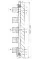
図1はこの発明の一実施形態としての半導体素子の平面図を示し、図2は図1のII−II線に沿う断面図を示す。この半導体素子は、CSP(chip size package)と呼ばれるものであり、平面正方形状のシリコン基板1を備えている。シリコン基板1の上面中央部には集積回路(図示せず)が設けられ、上面周辺部にはアルミニウム系金属などからなる複数の接続パッド2が集積回路に接続されて設けられている。
【0011】
接続パッド2の中央部を除くシリコン基板1の上面には酸化シリコンや窒化シリコンなどからなる絶縁膜3およびポリイミドなどからなる保護膜4が設けられている。接続パッド2の中央部は、絶縁膜3および保護膜4に設けられた開口部5を介して露出されている。
【0012】
開口部5を介して露出された接続パッド2の上面から保護膜4の上面の所定の箇所にかけて下地金属層6が設けられている。下地金属層6の上面には銅からなる再配線7が設けられている。再配線7の接続パッド部上面には銅からなるポスト電極8が設けられている。
【0013】
再配線7を含む保護膜4の上面にはエポキシ系樹脂などからなる封止膜9がその上面がポスト電極8の上面と面一となるように設けられている。したがって、ポスト電極8の上面は露出されている。この場合、ポスト電極8の平面形状は円形状となっている。そして、ポスト電極8の露出された上面には半田ボール10が設けられている。
【0014】
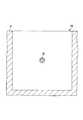
次に、図3は図1および図2に示す半導体素子を製造した際に同時に得られるアライメントマーク付素子の一例の平面図を示し、図4は図3のIV−IV線に沿う断面図を示す。このアライメントマーク付素子では、平面正方形状のシリコン基板1の上面に絶縁膜3および保護膜4が設けられ、保護膜4の上面中央部に下地金属層6およびアライメント用ポスト電極11が設けられ、保護膜4の上面に封止膜9がその上面がアライメント用ポスト電極11の上面と面一となるように設けられている。この場合、アライメント用ポスト電極11の平面形状は、ポスト電極8の平面形状である円形状と異なり、ほぼ十字形状となっている。
【0015】
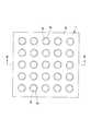
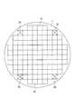
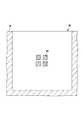
次に、上記構成の半導体素子の製造方法の一例について説明する。まず、図5に示すように、ウエハ状態のシリコン基板(半導体基板)1を用意する。ここで、図5において、縦線と横線とで囲まれた正方形状で無印の領域は、それぞれ、半導体集積回路が形成された半導体素子形成領域21であり、×印の領域はアライメントマーク形成領域22である。この場合、アライメントマーク形成領域22は、半導体素子形成領域21と同様、半導体集積回路が形成され、また、その平面サイズも半導体素子形成領域21と同じ平面サイズを有し、シリコン基板1の右上、右下、左上および左下の4箇所に設けられている。
【0016】
また、図6に示すように、シリコン基板1の半導体素子形成領域21の上面周辺部にはアルミニウム系金属などからなる接続パッド2が形成され、その上面の接続パッド2の中央部を除く領域には酸化シリコンなどからなる絶縁膜3およびポリイミドなどからなる保護膜4が形成され、絶縁膜3および保護膜4に形成された開口部5を介して露出された接続パッド2の上面を含む保護膜4の上面全体には下地金属層6が形成され、下地金属層6の上面の所定の箇所には銅からなる再配線7が形成されている。また、図7に示すように、シリコン基板1のアライメントマーク形成領域22の上面には絶縁膜3、保護膜4および下地金属層6が形成されている。
【0017】
次に、図8に示すように、再配線7を含む下地金属層6の上面全体にネガ型のメッキレジスト膜23を形成する。次に、露光を行なうが、この場合、露光マスクとして、図9および図10にそれぞれ示す第1および第2の露光マスク24、25を用意する。図9に示す第1の露光マスク24は、ポスト電極形成用であり、方形状のガラス板26の所定の領域で3行3列の合計9つの半導体素子形成領域21にそれぞれ対応する領域21aにおいてポスト電極8形成領域に対応する部分に円形状の遮光部27が形成され、且つ、当該領域の周囲全体に遮光部28が形成されたものからなっている。
【0018】
図10に示す第2の露光マスク25は、アライメント用ポスト電極形成用であり、方形状のガラス板29の所定の領域でアライメントマーク形成領域22に対応する領域22aにおいてアライメント用ポスト電極11形成領域に対応する部分に十字形状の遮光部30が形成され、且つ、当該領域の周囲全体に遮光部31が形成されたものからなっている。この場合、十字形状の遮光部30の十字を構成する2本の線の長さは第1の露光マスク24の円形状の遮光部27の直径よりも大きくなっており、同2本の線の幅は同円形状の遮光部27の直径よりも小さくなっている。
【0019】
一例として、第1の露光マスク24の円形状の遮光部27の直径が250μmであり、そのピッチが500μmである場合には、十字形状の遮光部30の十字を構成する2本の線の長さは500μmとし、同2本の線の幅は125μmとする。十字形状の遮光部30の十字を構成する2本の線の長さを第1の露光マスク24の円形状の遮光部27の直径よりも大きくしている理由は後述する。なお、図9および図10に示す第1および第2の露光マスク24、25はステップ露光用のものである。
【0020】
そして、まず、図9に示す第1の露光マスク24を用いて、図5に示す半導体素子形成領域21およびアライメントマーク形成領域22に対してステップ露光を行なう。すると、図11において円で示すように、半導体素子形成領域21では、メッキレジスト膜23のポスト電極8形成領域に対応する部分が非露光部23aとなる。また、アライメントマーク形成領域22におけるメッキレジスト膜23も、図11に示す半導体素子形成領域21におけるメッキレジスト膜23の場合と同様に露光される。この露光をショット単位毎に走査しながらシリコン基板1全面に亘り、順次、ステップ露光する。
【0021】
次に、図10に示す第2の露光マスク25を用いて、図5に示すアライメントマーク形成領域22のみに対して露光を行なう。すると、図12において白抜きのほぼ十字で示すように、アライメントマーク形成領域22では、メッキレジスト膜23のアライメント用ポスト電極11形成領域に対応する部分のみが非露光部23bとなる。すなわち、アライメントマーク形成領域22におけるメッキレジスト膜23は、第1および第2の露光マスク24、25を用いて2回露光されるため、その中心部のほぼ十字形状の部分のみが非露光部23bとなる。
【0022】
ここで、アライメントマーク形成領域22は、直径が250μmの円形の遮光部27を有する第1の露光マスク24を用いて露光されており、2回目の露光に用いる第2の露光マスク25は、それぞれ、500μmの長さの線を有する十字形状の遮光部30を有しているので、2回目の露光の際のマスク25の位置合わせには±120μmの許容公差が得られる。すなわち、遮光部30のアライメントマーク形状の十字の先端は非露光部23aに対する位置ずれが±120μm以内であれば非露光部23aより外側に位置するので、2回目の露光によって図12に図示する非露光部23bの十字部の直径が250μm以下となることは無い。十字形状の遮光部30の十字を構成する2本の線の長さを第1の露光マスク24の円形状の遮光部27の直径よりも大きくしている理由はこのためである。この第2の露光マスク25を用いた露光は、各アライメントマーク形成領域22に対し行うもので、計4回行う。
【0023】
次に、現像を行なうと、図13に示すように、半導体素子形成領域21では、再配線7の接続パッド部つまりポスト電極8形成領域に対応する領域におけるメッキレジスト膜23に開口部32が形成される。また、図14に示すように、アライメントマーク形成領域22では、アライメント用ポスト電極11形成領域に対応する領域におけるメッキレジスト膜23に開口部33が形成される。
【0024】
次に、下地金属層6をメッキ電流路として銅の電解メッキを行うと、図13に示すように、半導体素子形成領域21では、メッキレジスト膜23の開口部32内における再配線7の接続パッド部上面にポスト電極8が形成される。また、図14に示すように、アライメントマーク形成領域22では、メッキレジスト膜23の開口部33内における下地金属層6の上面にアライメント用ポスト電極11が形成される。次に、メッキレジスト膜23を剥離する。
【0025】
次に、再配線7およびアライメント用ポスト電極11をマスクとして下地金属層6の不要な部分をエッチングして除去すると、図15に示すように、半導体素子形成領域21では、再配線7下にのみ下地金属層6が残存され、また、図16に示すように、アライメントマーク形成領域22では、アライメント用ポスト電極11下にのみ下地金属層6が残存される。
【0026】
次に、図17に示すように、ポスト電極8および再配線7(およびアライメント用ポスト電極11)を含む保護膜4の上面全体にエポキシ系樹脂などからなる封止膜9をその厚さがポスト電極8(およびアライメント用ポスト電極11)の高さよりもやや厚くなるように形成する。したがって、この状態では、ポスト電極8(およびアライメント用ポスト電極11)の上面は封止膜9によって覆われている。
【0027】
次に、封止膜9およびポスト電極8(およびアライメント用ポスト電極11)の上面側を適宜に研磨して除去することにより、図18に示すように、ポスト電極8(およびアライメント用ポスト電極11)の上面を露出させるとともに、この露出されたポスト電極8(およびアライメント用ポスト電極11)の上面を封止膜9の上面と面一とする。
【0028】
次に、図19に示すように、ポスト電極8の上面に半田ボール10を形成する。次に、シリコン基板1の下面において各半導体素子形成領域21に対応する領域の所定の箇所に所定のマーク(捺印)を形成する。次に、ダイシング工程を経ると、図1および図2に示す半導体素子が複数個得られ、また、図3および図4に示すアライメントマーク付素子が4個得られる。
【0029】
ところで、ポスト電極8形成工程後における半田ボール10形成工程、マーク(捺印)形成工程およびダイシング工程では、ウエハ状態のシリコン基板1の位置合わせを行なう必要がある。また、各ポスト電極8の上面に半田ボール10を形成する前に、各ポスト電極8の上面に半田層を印刷する場合があり、この場合にも、位置合わせが必要である。さらに、マーク(捺印)形成工程後でダイシング工程前に電気的コンタクト検査工程を行なう場合も、ウエハ状態のシリコン基板1の位置合わせを行なう必要がある。このような場合には、アライメントマーク形成領域22に形成されたアライメント用ポスト電極11をアライメントマークとして使用する。
【0030】
すなわち、ポスト電極8が形成された半導体素子形成領域21と同じ平面サイズを有するアライメントマーク形成領域22にアライメント用ポスト電極11を形成しているので、ステップ露光方式を採用しても、ウエハ状態のシリコン基板1の位置合わせを行なうとき、アライメントマーク形成領域22に形成されたアライメント用ポスト電極11をアライメントマークとして容易に認識することができ、アライメントマーク誤認識の発生を防止することができる。
【0031】
しかも、この場合、アライメント用ポスト電極11の平面形状を、ポスト電極8の平面形状である円形状と異なり、ほぼ十字形状としているので、アライメント用ポスト電極11とポスト電極8とを混同することがなく、アライメントマーク誤認識の発生を確実に防止することができる。
【0032】
なお、例えば、図20に示すこの発明の他の実施形態のように、アライメントマーク形成領域22の周囲における○印の領域を、半導体素子形成領域21と同じ平面サイズを有し、ポスト電極を有しない非半導体素子形成領域41としてもよい。このようにした場合には、アライメントマーク形成領域22と半導体素子形成領域21との間にポスト電極を有しない非半導体素子形成領域41が介在することにより、アライメントマーク誤認識の発生をより一層確実に防止することができる。
【0033】
次に、図20に示す非半導体素子形成領域41の形成方法について説明する。この場合には、予め、第1、第2の露光マスク24、25の他に、図21に示す第3の露光マスク42を用意する。この第3の露光マスク42では、方形状のガラス板43の所定の領域で非半導体素子形成領域41に対応する領域のすべてが透過部44となっており、この透過部44の周囲全体に遮光部45が形成されている。
【0034】
先ず、第1の露光マスク24を用いて、シリコン基板1全面の半導体素子形成領域21およびアライメントマーク形成領域22に対してステップ露光を行なう。次に、第2の露光マスク25を用いて、4箇所のアライメントマーク形成領域22に対する露光を行う。これにより、第1実施例にて説明した如く、各アライメントマーク形成領域22は、図12に示す非露光部23bを除く全ての領域が露光される。
【0035】
そして、この後、第3の露光マスク42を用いて、該第3の露光マスク42の透過部44の縁部を非半導体素子形成領域41の縁部に位置合わせして露光を行なう。第3の露光マスク42による位置合わせおよび露光は、順次、各非半導体素子形成領域41に対して移動してその全てに対して行う。この露光により、非半導体素子形成領域41におけるメッキレジスト膜全体が露光部となり、現像を行なっても、当該領域におけるメッキレジスト膜に開口部は形成されない。したがって、電解メッキを行なっても、当該領域にはポスト電極は形成されず、非半導体素子形成領域41となる。この場合、非半導体素子形成領域41では、保護膜の上面全体には当初下地金属層が形成されているが、下地金属層の上面には再配線は形成されておらず、また、上述の如く、ポスト電極も形成されないため、保護膜の上面全体に当初形成されていた下地金属層はすべて除去される。
【0036】
なお、第2の露光マスク25として、例えば、図22に示すように、第1の露光マスク24の円形状の遮光部27と同一径あるいはそれよりもやや大径の円形状の遮光部30が形成されたものを用いた場合には、図23において円で示すように、アライメントマーク形成領域22では、メッキレジスト膜23のアライメント用ポスト電極形成領域に対応する部分のみが非露光部23cとなり、これに対応する平面形状、すなわち、ポスト電極8の平面形状と全く同じ平面形状である円形状のアライメント用ポスト電極が形成されることになる。ただし、この場合も、アライメント用ポスト電極はアライメントマーク形成領域22に形成されるため、アライメントマークとして容易に認識することができ、アライメントマーク誤認識の発生を防止することができる。また、アライメント用ポスト電極の平面形状は、三角形状、四角形状、その他の形状などとしてもよい。
【0037】
また、第2の露光マスク25として、例えば、図24に示すように、4つの正方形状の遮光部30間に十字形状の透過部が形成されたものを用いた場合には、図25において4つの1/4円で示すように、アライメントマーク形成領域22では、メッキレジスト膜23のアライメント用ポスト電極形成領域に対応する部分のみが非露光部23dとなり、これに対応する平面形状のアライメント用ポスト電極が形成されることになる。
【0038】
さらに、露光マスクとしては、第1の露光マスク24と第2の露光マスク25とを1枚のガラス板に形成したものを用いてもよく、また、第1の露光マスク24と第2の露光マスク25と第3の露光マスク42とを1枚のガラス板に形成したものを用いてもよい。
【0039】
【発明の効果】
以上説明した通り、この発明によれば、ポスト電極が形成された半導体素子形成領域と同じ平面サイズを有するアライメントマーク形成領域にアライメント用ポスト電極とを備え、前記アライメントマーク形成領域の周囲に、前記半導体素子形成領域と同じ平面サイズを有し、ポスト電極を有しない複数の非半導体素子形成領域が設けられているので、ポスト電極形成後においてアライメントマークを確実に認識し、アライメントを効率的に行うことができる。
【図面の簡単な説明】
【図1】この発明の一実施形態としての半導体素子の平面図。
【図2】図1のII−II線に沿う断面図。
【図3】図1および図2に示す半導体素子を製造した際に同時に得られるアライメントマーク付素子の一例の平面図。
【図4】図3のIV−IV線に沿う断面図。
【図5】上記一実施形態における半導体素子の製造に際し、当初用意したウエハ状態のシリコン基板の平面図。
【図6】図5に示す半導体素子形成領域の部分の断面図。
【図7】図5に示すアライメントマーク形成領域の部分の断面図。
【図8】図6に続く工程で半導体素子形成領域の部分を示す断面図。
【図9】第1の露光マスクの平面図。
【図10】第2の露光マスクの平面図。
【図11】半導体素子形成領域の部分におけるメッキレジスト膜の露光状態を説明するために示す平面図。
【図12】アライメントマーク形成領域の部分におけるメッキレジスト膜の露光状態を説明するために示す平面図。
【図13】図8に続く工程で半導体素子形成領域の部分を示す断面図。
【図14】図13と同一の工程でアライメントマーク形成領域の部分を示す断面図。
【図15】図13に続く工程で半導体素子形成領域の部分を示す断面図。
【図16】図15と同一の工程でアライメントマーク形成領域の部分を示す断面図。
【図17】図15に続く工程で半導体素子形成領域の部分を示す断面図。
【図18】図17に続く工程で半導体素子形成領域の部分を示す断面図。
【図19】図18に続く工程で半導体素子形成領域の部分を示す断面図。
【図20】この発明の他の実施形態を説明するために示すウエハ状態のシリコン基板の平面図。
【図21】第3の露光マスクの平面図。
【図22】第2の露光マスクの他の例の平面図。
【図23】図22に示す第2の露光マスクを用いた場合のアライメントマーク形成領域の部分におけるメッキレジスト膜の露光状態を説明するために示す平面図。
【図24】第2の露光マスクのさらに他の例の平面図。
【図25】図24に示す第2の露光マスクを用いた場合のアライメントマーク形成領域の部分におけるメッキレジスト膜の露光状態を説明するために示す平面図。
【符号の説明】
1 シリコン基板
6 下地金属層
7 再配線
8 ポスト電極
9 封止膜
10 半田ボール
11 アライメント用ポスト電極
21 半導体素子形成領域
22 アライメントマーク形成領域
23 メッキレジスト膜
24 第1の露光マスク
25 第2の露光マスク
41 非半導体素子形成領域
42 第3の露光マスク[0001]
BACKGROUND OF THE INVENTION
The present invention relatesto a semiconductor substrate.
[0002]
[Prior art]
Conventionally, when a post electrode for external connection is formed on a connection pad formed on a semiconductor integrated circuit wafer, the alignment of the photomask has a large error when the orientation flat of the wafer is used. This is done based on the opening of the insulating film covering the peripheral edge. However, as the number of post electrodes increases or the arrangement pitch becomes smaller, it is difficult to maintain accuracy even with alignment based on the opening of the insulating film. For this reason, there is an improvement in which an alignment mark is directly formed on a connection pad (see, for example, Patent Document 1).
[0003]
In the method described in
[0004]
[Patent Document 1]
Japanese Patent Laid-Open No. 11-195667
[Problems to be solved by the invention]
By the way, in recent years, after forming a post electrode on the entire surface of the semiconductor integrated circuit wafer, a sealing material is formed on the entire surface of the semiconductor integrated circuit wafer, and all the post electrodes are filled with this sealing material to perform packaging. Later, a so-called wafer level package (WLP) has been developed in which each semiconductor integrated circuit element is separated by dicing. In this wafer level package, a sealing material is deposited on a semiconductor integrated circuit wafer, polished to expose the top surface of the post electrode and flatten the sealing material, and then solder printing and soldering on the top surface of each post electrode There are processes that require alignment after the formation of the post electrodes, such as ball mounting and marking on the back of the package.
[0006]
However, in the method described in
[0007]
For this reason, the alignment in each step after the formation of the post electrode is performed by using the shape of the upper surface of the post electrode exposed from the sealing material as an alignment mark. It was difficult to discriminate from the electrode, and the recognition rate was high.
[0008]
Accordingly, an object of the present invention is to provide a semiconductor substrate, a semiconductor substrate manufacturing method, and a semiconductor element manufacturing method capable of reliably recognizing an alignment mark and performing alignment efficiently after forming a post electrode. To do.
[0009]
[Means for Solving the Problems]
The present invention includes a plurality of semiconductor element formation regions each having a plurality of post electrodes, and an alignment mark formation region having the same planar size as the semiconductor element formation region and having an alignment post electrode. Around the region, a plurality of non-semiconductor element formation regions having the same planar size as the semiconductor element formation region and having no post electrode are provided.
According to the present invention, the alignment mark forming region having the same planar size as the semiconductor element forming region in which the post electrode is formedis provided with the alignment post electrode,and the semiconductor element forming is formed around the alignment mark forming region. Since a plurality of non-semiconductor element formation regions having the same planar size as the region and having no post electrodes are provided , alignment marks can be reliably recognized after the formation of the post electrodes, and alignment can be performed efficiently. .
[0010]
DETAILED DESCRIPTION OF THE INVENTION
FIG. 1 is a plan view of a semiconductor element as one embodiment of the present invention, and FIG. 2 is a cross-sectional view taken along line II-II in FIG. This semiconductor element is called a CSP (chip size package) and includes a
[0011]
An
[0012]
A
[0013]
A
[0014]
Next, FIG. 3 shows a plan view of an example of an element with an alignment mark obtained at the same time when the semiconductor element shown in FIGS. 1 and 2 is manufactured, and FIG. 4 is a sectional view taken along line IV-IV in FIG. Show. In this element with an alignment mark, an
[0015]
Next, an example of a method for manufacturing the semiconductor element having the above configuration will be described. First, as shown in FIG. 5, a silicon substrate (semiconductor substrate) 1 in a wafer state is prepared. Here, in FIG. 5, the square and unmarked regions surrounded by the vertical lines and the horizontal lines are the semiconductor
[0016]
Further, as shown in FIG. 6, a
[0017]
Next, as shown in FIG. 8, a negative type plating resist
[0018]
The
[0019]
As an example, when the diameter of the circular light-shielding
[0020]
First, step exposure is performed on the semiconductor
[0021]
Next, only the alignment
[0022]
Here, the alignment
[0023]
Next, when development is performed, as shown in FIG. 13, in the semiconductor
[0024]
Next, when copper electroplating is performed using the
[0025]
Next, when unnecessary portions of the
[0026]
Next, as shown in FIG. 17, a sealing
[0027]
Next, the upper surface side of the sealing
[0028]
Next, as shown in FIG. 19,
[0029]
Incidentally, in the
[0030]
That is, since the
[0031]
In addition, in this case, the planar shape of the
[0032]
For example, as in another embodiment of the present invention shown in FIG. 20, the circled region around the alignment
[0033]
Next, a method for forming the non-semiconductor
[0034]
First, step exposure is performed on the semiconductor
[0035]
Thereafter, exposure is performed using the
[0036]
As the
[0037]
In addition, when the
[0038]
Further, as the exposure mask, a mask in which the
[0039]
【The invention's effect】
As described above, according to the present invention, the alignment mark forming region having the same planar size as the semiconductor element forming region in which the post electrode is formed includes the alignment post electrode,and the periphery of the alignment mark forming region Since a plurality of non-semiconductor element formation regions having the same planar size as the semiconductor element formation region and no post electrodes are provided , alignment marks are reliably recognized after the post electrodes are formed, and alignment is performed efficiently. be able to.
[Brief description of the drawings]
FIG. 1 is a plan view of a semiconductor element as one embodiment of the present invention.
2 is a cross-sectional view taken along line II-II in FIG.
FIG. 3 is a plan view of an example of an element with an alignment mark obtained simultaneously when the semiconductor element shown in FIGS. 1 and 2 is manufactured.
4 is a cross-sectional view taken along line IV-IV in FIG.
FIG. 5 is a plan view of a silicon substrate prepared in a wafer state at the time of manufacturing a semiconductor element in the embodiment.
6 is a cross-sectional view of a portion of the semiconductor element formation region shown in FIG.
7 is a cross-sectional view of a portion of the alignment mark formation region shown in FIG.
8 is a cross-sectional view showing a part of a semiconductor element formation region in a process following FIG. 6;
FIG. 9 is a plan view of a first exposure mask.
FIG. 10 is a plan view of a second exposure mask.
FIG. 11 is a plan view for explaining an exposure state of a plating resist film in a semiconductor element formation region.
FIG. 12 is a plan view for explaining the exposure state of the plating resist film in the alignment mark formation region.
13 is a cross-sectional view showing a part of a semiconductor element formation region in the process following FIG. 8;
14 is a cross-sectional view showing a portion of an alignment mark formation region in the same process as FIG. 13;
15 is a cross-sectional view showing a part of a semiconductor element formation region in the process following FIG. 13;
16 is a cross-sectional view showing a portion of an alignment mark formation region in the same process as FIG.
17 is a cross-sectional view showing a part of a semiconductor element formation region in a process following FIG. 15;
18 is a cross-sectional view showing a part of a semiconductor element formation region in the process following FIG. 17;
FIG. 19 is a cross-sectional view showing a part of a semiconductor element formation region in the process following FIG. 18;
FIG. 20 is a plan view of a silicon substrate in a wafer state for explaining another embodiment of the present invention.
FIG. 21 is a plan view of a third exposure mask.
FIG. 22 is a plan view of another example of the second exposure mask.
FIG. 23 is a plan view for explaining the exposure state of the plating resist film in the alignment mark formation region when the second exposure mask shown in FIG. 22 is used.
FIG. 24 is a plan view of still another example of the second exposure mask.
FIG. 25 is a plan view for explaining the exposure state of the plating resist film in the alignment mark formation region when the second exposure mask shown in FIG. 24 is used.
[Explanation of symbols]
DESCRIPTION OF
Claims (1)
Translated fromJapanesePriority Applications (7)
| Application Number | Priority Date | Filing Date | Title |
|---|---|---|---|
| JP2003147448AJP3988679B2 (en) | 2003-05-26 | 2003-05-26 | Semiconductor substrate |
| US10/853,728US20040238973A1 (en) | 2003-05-26 | 2004-05-24 | Semiconductor device having alignment post electrode and method of manufacturing the same |
| KR1020040037103AKR100610555B1 (en) | 2003-05-26 | 2004-05-25 | Semiconductor element and method of manufacturing the same |
| CN 200610162516CN100499094C (en) | 2003-05-26 | 2004-05-26 | Semiconductor element |
| TW093114867ATWI248144B (en) | 2003-05-26 | 2004-05-26 | Semiconductor element having alignment post electrode and method of manufacturing the same |
| CNB2004100631607ACN100352048C (en) | 2003-05-26 | 2004-05-26 | Semiconductor element and its manufacturing method |
| US11/656,866US7944064B2 (en) | 2003-05-26 | 2007-01-22 | Semiconductor device having alignment post electrode and method of manufacturing the same |
Applications Claiming Priority (1)
| Application Number | Priority Date | Filing Date | Title |
|---|---|---|---|
| JP2003147448AJP3988679B2 (en) | 2003-05-26 | 2003-05-26 | Semiconductor substrate |
Related Child Applications (2)
| Application Number | Title | Priority Date | Filing Date |
|---|---|---|---|
| JP2007131207ADivisionJP4341694B2 (en) | 2007-05-17 | 2007-05-17 | Manufacturing method of semiconductor device |
| JP2007131206ADivisionJP4506780B2 (en) | 2007-05-17 | 2007-05-17 | Manufacturing method of semiconductor substrate |
Publications (2)
| Publication Number | Publication Date |
|---|---|
| JP2004349611A JP2004349611A (en) | 2004-12-09 |
| JP3988679B2true JP3988679B2 (en) | 2007-10-10 |
Family
ID=33533969
Family Applications (1)
| Application Number | Title | Priority Date | Filing Date |
|---|---|---|---|
| JP2003147448AExpired - Fee RelatedJP3988679B2 (en) | 2003-05-26 | 2003-05-26 | Semiconductor substrate |
Country Status (2)
| Country | Link |
|---|---|
| JP (1) | JP3988679B2 (en) |
| CN (1) | CN100499094C (en) |
Families Citing this family (6)
| Publication number | Priority date | Publication date | Assignee | Title |
|---|---|---|---|---|
| JP5247998B2 (en)* | 2006-08-11 | 2013-07-24 | 株式会社テラミクロス | Manufacturing method of semiconductor device |
| WO2009007932A2 (en) | 2007-07-12 | 2009-01-15 | Nxp B.V. | Integrated circuits on a wafer and method of producing integrated circuits |
| JP5126231B2 (en) | 2007-08-10 | 2013-01-23 | 富士通セミコンダクター株式会社 | Semiconductor element selection and acquisition method, semiconductor device manufacturing method, and semiconductor device |
| JP2009266995A (en)* | 2008-04-24 | 2009-11-12 | Casio Comput Co Ltd | Manufacturing method of semiconductor device |
| JP6678506B2 (en)* | 2016-04-28 | 2020-04-08 | 株式会社アムコー・テクノロジー・ジャパン | Semiconductor package and method of manufacturing semiconductor package |
| JP6559841B1 (en)* | 2018-06-01 | 2019-08-14 | エイブリック株式会社 | Semiconductor device |
- 2003
- 2003-05-26JPJP2003147448Apatent/JP3988679B2/ennot_activeExpired - Fee Related
- 2004
- 2004-05-26CNCN 200610162516patent/CN100499094C/ennot_activeExpired - Lifetime
Also Published As
| Publication number | Publication date |
|---|---|
| CN100499094C (en) | 2009-06-10 |
| CN1953167A (en) | 2007-04-25 |
| JP2004349611A (en) | 2004-12-09 |
Similar Documents
| Publication | Publication Date | Title |
|---|---|---|
| US7944064B2 (en) | Semiconductor device having alignment post electrode and method of manufacturing the same | |
| JP3989869B2 (en) | Semiconductor device and manufacturing method thereof | |
| US7582972B2 (en) | Semiconductor device and fabrication method thereof | |
| KR100858386B1 (en) | Substrate for forming semiconductor element and manufacturing method of the semiconductor element | |
| KR20110139087A (en) | Semiconductor device and manufacturing method thereof | |
| US10957638B2 (en) | Device with pillar-shaped components | |
| JP3988679B2 (en) | Semiconductor substrate | |
| US7030508B2 (en) | Substrate for semiconductor package and wire bonding method using thereof | |
| KR20130126171A (en) | Bump structures and methods of forming them | |
| US7250329B2 (en) | Method of fabricating a built-in chip type substrate | |
| KR100610555B1 (en) | Semiconductor element and method of manufacturing the same | |
| JP5247998B2 (en) | Manufacturing method of semiconductor device | |
| JP2005012065A (en) | Semiconductor device and its manufacturing method | |
| JP4292041B2 (en) | Semiconductor substrate, semiconductor substrate manufacturing method, and semiconductor device manufacturing method | |
| JP4341694B2 (en) | Manufacturing method of semiconductor device | |
| JP4506780B2 (en) | Manufacturing method of semiconductor substrate | |
| JP4987910B2 (en) | Method for manufacturing solder layer of semiconductor element, method for manufacturing mark of semiconductor element, and method for dicing semiconductor element | |
| KR20110014962A (en) | Semiconductor device and manufacturing method thereof | |
| JP2007116203A (en) | Manufacturing method of semiconductor device | |
| JP2005294546A (en) | Plating pattern forming method |
Legal Events
| Date | Code | Title | Description |
|---|---|---|---|
| A621 | Written request for application examination | Free format text:JAPANESE INTERMEDIATE CODE: A621 Effective date:20050317 | |
| RD02 | Notification of acceptance of power of attorney | Free format text:JAPANESE INTERMEDIATE CODE: A7422 Effective date:20060208 | |
| RD04 | Notification of resignation of power of attorney | Free format text:JAPANESE INTERMEDIATE CODE: A7424 Effective date:20060405 | |
| A977 | Report on retrieval | Free format text:JAPANESE INTERMEDIATE CODE: A971007 Effective date:20060714 | |
| A131 | Notification of reasons for refusal | Free format text:JAPANESE INTERMEDIATE CODE: A131 Effective date:20061212 | |
| A521 | Written amendment | Free format text:JAPANESE INTERMEDIATE CODE: A523 Effective date:20070118 | |
| A131 | Notification of reasons for refusal | Free format text:JAPANESE INTERMEDIATE CODE: A131 Effective date:20070320 | |
| A521 | Written amendment | Free format text:JAPANESE INTERMEDIATE CODE: A523 Effective date:20070517 | |
| TRDD | Decision of grant or rejection written | ||
| A01 | Written decision to grant a patent or to grant a registration (utility model) | Free format text:JAPANESE INTERMEDIATE CODE: A01 Effective date:20070626 | |
| A61 | First payment of annual fees (during grant procedure) | Free format text:JAPANESE INTERMEDIATE CODE: A61 Effective date:20070709 | |
| FPAY | Renewal fee payment (prs date is renewal date of database) | Free format text:PAYMENT UNTIL: 20100727 Year of fee payment:3 | |
| R150 | Certificate of patent (=grant) or registration of utility model | Free format text:JAPANESE INTERMEDIATE CODE: R150 | |
| FPAY | Renewal fee payment (prs date is renewal date of database) | Free format text:PAYMENT UNTIL: 20110727 Year of fee payment:4 | |
| FPAY | Renewal fee payment (prs date is renewal date of database) | Free format text:PAYMENT UNTIL: 20110727 Year of fee payment:4 | |
| FPAY | Renewal fee payment (prs date is renewal date of database) | Free format text:PAYMENT UNTIL: 20120727 Year of fee payment:5 | |
| FPAY | Renewal fee payment (prs date is renewal date of database) | Free format text:PAYMENT UNTIL: 20120727 Year of fee payment:5 | |
| FPAY | Renewal fee payment (prs date is renewal date of database) | Free format text:PAYMENT UNTIL: 20120727 Year of fee payment:5 | |
| S111 | Request for change of ownership or part of ownership | Free format text:JAPANESE INTERMEDIATE CODE: R313111 | |
| FPAY | Renewal fee payment (prs date is renewal date of database) | Free format text:PAYMENT UNTIL: 20120727 Year of fee payment:5 | |
| R350 | Written notification of registration of transfer | Free format text:JAPANESE INTERMEDIATE CODE: R350 | |
| FPAY | Renewal fee payment (prs date is renewal date of database) | Free format text:PAYMENT UNTIL: 20130727 Year of fee payment:6 | |
| LAPS | Cancellation because of no payment of annual fees |