JP3985346B2 - Projection exposure apparatus, projection exposure apparatus adjustment method, and projection exposure method - Google Patents
Projection exposure apparatus, projection exposure apparatus adjustment method, and projection exposure methodDownload PDFInfo
- Publication number
- JP3985346B2 JP3985346B2JP18149898AJP18149898AJP3985346B2JP 3985346 B2JP3985346 B2JP 3985346B2JP 18149898 AJP18149898 AJP 18149898AJP 18149898 AJP18149898 AJP 18149898AJP 3985346 B2JP3985346 B2JP 3985346B2
- Authority
- JP
- Japan
- Prior art keywords
- light
- optical system
- projection exposure
- exposure apparatus
- projection
- Prior art date
- Legal status (The legal status is an assumption and is not a legal conclusion. Google has not performed a legal analysis and makes no representation as to the accuracy of the status listed.)
- Expired - Lifetime
Links
Images

Classifications
- G—PHYSICS
- G02—OPTICS
- G02B—OPTICAL ELEMENTS, SYSTEMS OR APPARATUS
- G02B17/00—Systems with reflecting surfaces, with or without refracting elements
- G02B17/08—Catadioptric systems
- G02B17/0892—Catadioptric systems specially adapted for the UV
- G—PHYSICS
- G02—OPTICS
- G02B—OPTICAL ELEMENTS, SYSTEMS OR APPARATUS
- G02B13/00—Optical objectives specially designed for the purposes specified below
- G02B13/14—Optical objectives specially designed for the purposes specified below for use with infrared or ultraviolet radiation
- G02B13/143—Optical objectives specially designed for the purposes specified below for use with infrared or ultraviolet radiation for use with ultraviolet radiation
- G—PHYSICS
- G02—OPTICS
- G02B—OPTICAL ELEMENTS, SYSTEMS OR APPARATUS
- G02B17/00—Systems with reflecting surfaces, with or without refracting elements
- G02B17/08—Catadioptric systems
- G—PHYSICS
- G03—PHOTOGRAPHY; CINEMATOGRAPHY; ANALOGOUS TECHNIQUES USING WAVES OTHER THAN OPTICAL WAVES; ELECTROGRAPHY; HOLOGRAPHY
- G03F—PHOTOMECHANICAL PRODUCTION OF TEXTURED OR PATTERNED SURFACES, e.g. FOR PRINTING, FOR PROCESSING OF SEMICONDUCTOR DEVICES; MATERIALS THEREFOR; ORIGINALS THEREFOR; APPARATUS SPECIALLY ADAPTED THEREFOR
- G03F7/00—Photomechanical, e.g. photolithographic, production of textured or patterned surfaces, e.g. printing surfaces; Materials therefor, e.g. comprising photoresists; Apparatus specially adapted therefor
- G03F7/70—Microphotolithographic exposure; Apparatus therefor
- G03F7/70058—Mask illumination systems
- G03F7/70091—Illumination settings, i.e. intensity distribution in the pupil plane or angular distribution in the field plane; On-axis or off-axis settings, e.g. annular, dipole or quadrupole settings; Partial coherence control, i.e. sigma or numerical aperture [NA]
- G03F7/70108—Off-axis setting using a light-guiding element, e.g. diffractive optical elements [DOEs] or light guides
- G—PHYSICS
- G03—PHOTOGRAPHY; CINEMATOGRAPHY; ANALOGOUS TECHNIQUES USING WAVES OTHER THAN OPTICAL WAVES; ELECTROGRAPHY; HOLOGRAPHY
- G03F—PHOTOMECHANICAL PRODUCTION OF TEXTURED OR PATTERNED SURFACES, e.g. FOR PRINTING, FOR PROCESSING OF SEMICONDUCTOR DEVICES; MATERIALS THEREFOR; ORIGINALS THEREFOR; APPARATUS SPECIALLY ADAPTED THEREFOR
- G03F7/00—Photomechanical, e.g. photolithographic, production of textured or patterned surfaces, e.g. printing surfaces; Materials therefor, e.g. comprising photoresists; Apparatus specially adapted therefor
- G03F7/70—Microphotolithographic exposure; Apparatus therefor
- G03F7/70216—Mask projection systems
- G03F7/70225—Optical aspects of catadioptric systems, i.e. comprising reflective and refractive elements
- G—PHYSICS
- G03—PHOTOGRAPHY; CINEMATOGRAPHY; ANALOGOUS TECHNIQUES USING WAVES OTHER THAN OPTICAL WAVES; ELECTROGRAPHY; HOLOGRAPHY
- G03F—PHOTOMECHANICAL PRODUCTION OF TEXTURED OR PATTERNED SURFACES, e.g. FOR PRINTING, FOR PROCESSING OF SEMICONDUCTOR DEVICES; MATERIALS THEREFOR; ORIGINALS THEREFOR; APPARATUS SPECIALLY ADAPTED THEREFOR
- G03F7/00—Photomechanical, e.g. photolithographic, production of textured or patterned surfaces, e.g. printing surfaces; Materials therefor, e.g. comprising photoresists; Apparatus specially adapted therefor
- G03F7/70—Microphotolithographic exposure; Apparatus therefor
- G03F7/70216—Mask projection systems
- G03F7/70275—Multiple projection paths, e.g. array of projection systems, microlens projection systems or tandem projection systems
- G—PHYSICS
- G03—PHOTOGRAPHY; CINEMATOGRAPHY; ANALOGOUS TECHNIQUES USING WAVES OTHER THAN OPTICAL WAVES; ELECTROGRAPHY; HOLOGRAPHY
- G03F—PHOTOMECHANICAL PRODUCTION OF TEXTURED OR PATTERNED SURFACES, e.g. FOR PRINTING, FOR PROCESSING OF SEMICONDUCTOR DEVICES; MATERIALS THEREFOR; ORIGINALS THEREFOR; APPARATUS SPECIALLY ADAPTED THEREFOR
- G03F7/00—Photomechanical, e.g. photolithographic, production of textured or patterned surfaces, e.g. printing surfaces; Materials therefor, e.g. comprising photoresists; Apparatus specially adapted therefor
- G03F7/70—Microphotolithographic exposure; Apparatus therefor
- G03F7/70483—Information management; Active and passive control; Testing; Wafer monitoring, e.g. pattern monitoring
- G03F7/7055—Exposure light control in all parts of the microlithographic apparatus, e.g. pulse length control or light interruption
- G03F7/70566—Polarisation control
Landscapes
- Physics & Mathematics (AREA)
- General Physics & Mathematics (AREA)
- Optics & Photonics (AREA)
- Health & Medical Sciences (AREA)
- Toxicology (AREA)
- Exposure And Positioning Against Photoresist Photosensitive Materials (AREA)
- Exposure Of Semiconductors, Excluding Electron Or Ion Beam Exposure (AREA)
- Lenses (AREA)
- Liquid Crystal (AREA)
- Non-Portable Lighting Devices Or Systems Thereof (AREA)
Abstract
Description
Translated fromJapanese【0001】
【発明の属する技術分野】
本発明は、例えば半導体素子、または液晶表示素子等をフォトリソグラフィ工程で製造する際に使用される投影露光装置に関し、特に投影光学系の要素として反射系を用いることにより、紫外線波長域で0.1ミクロン単位の解像度を有する反射屈折型投影光学系を備える投影露光装置に関する。
【0002】
【従来の技術】
半導体素子等を製造するためのフォトリソグラフィ工程においては、フォトマスクまたはレチクル(以下、レチクルと総称する。)上のパターンの像を、投影光学系を介して、フォトレジスト等が塗布されたウエハまたはガラスプレート等(以下、ウエハと総称する。)上に露光する投影露光装置が使用されている。半導体素子等の集積度が向上するにつれて、投影露光装置に使用されている投影光学系に要求される解像力は益々高まっている。この要求を満足するために、照明光の波長を短くし、且つ投影光学系の開口数(N.A.)を大きくする必要が生じた。
【0003】
しかし、照明光の波長が短くなると、光の吸収によって実用に耐える硝材の種類は限られ、波長が300nm以下になると、現在のところ実用上使える硝材は合成石英と蛍石だけとなる。両者のアッベ数は、色収差を補正するのに十分な程は離れていないので、色収差の補正が困難となる。
また求められる光学性能は極めて高いため、各収差をほぼ無収差にすることが必要となる。これをレンズ群のみで構成される屈折光学系で達成するためには、多数のレンズが必要となり、透過率の低減や光学系を製造するためのコストの増大を避けることはできない。
【0004】
これに対して凹面鏡等のパワーを用いた反射光学系は色収差がなく、しかもレンズとは逆のペッツバール和への寄与を示すため、反射光学系と屈折光学系とを組み合わせたいわゆる反射屈折光学系によれば、レンズ枚数の増加を招くことなく、色収差をはじめとする各種の収差をほぼ無収差にすることができる。こうした反射屈折光学系により投影光学系を構成する種々の技術が提案されてきている。その中で、光学系の途中で1回中間像を形成するタイプとしては、特開昭63−163319号公報、特公平7−111512号公報、特公平5−25170号公報、USP−4,779,966等が開示されている。
【0005】
【発明が解決しようとする課題】
上記の如き従来の技術では、収差補正のために凹面鏡等の球面鏡が必ず用いられる。そのため、レチクルから球面鏡に向かう光の光路と、球面鏡から戻る反射光の光路とを分離して、球面鏡から戻る反射光の光路をウエハ方向に偏向させる必要がある。それ故、反射膜のコーティングされた1つまたは複数の平面鏡が必要となる。しかし光線を偏向する平面鏡は、P偏光に対する反射率とS偏光に対する反射率とが異なる。
特に露光波長が短くなると、膜材料の減少等により、反射膜によるP偏光とS偏光に対する反射率の差が大きくなり、この結果、方向性をもった偏光光が生じてしまう。投影露光に方向性をもった偏光光を用いると、レチクルパターンの方向性により結像性能が変化してしまう。結像性能の変化量は開口数に比例し、通常の投影光学系は縮小倍率を持っているために、ウエハ側でより大きな開口数を持つ。したがってこの場合には、ウエハ上での結像性能の変化が顕著となり、フォトリソグラフィ工程において大きな問題となる。
本発明はかかる点に鑑み、紫外線波長域で大きな開口数を達成し、光学系が実用的な大きさで、レチクルパターンの方向性に依存せず、0.1ミクロン単位の解像度を有する反射屈折型投影光学系を備える投影露光装置を提供することを課題とする。
【0006】
【課題を解決するための手段】
上述の課題を達成するために、本発明は、投影原版上に形成されたパターンを照明する照明光学系と、1又は複数の球面鏡と複数のレンズと1又は複数の平面鏡とを有し、前記パターンの像を被露光物体の感光面上に形成する反射屈折型投影光学系とを備えた投影露光装置において、前記照明光学系は、前記反射屈折型投影光学系から前記感光面へ向かう光の偏光状態をほぼ非偏光にするために、前記パターンを部分偏光光によって照明するように構成されたことを特徴とする投影露光装置とした。
また、本発明は、光源からの光に基づいて、所定のパターンの像を被露光物体の感光面上に形成する投影露光装置であって、前記光源と前記被露光物体との間の光路中に配置されて、入射光を偏向する平面鏡と、前記感光面をほぼ非偏光で露光するように、前記平面鏡へ入射する入射光の偏光度を制御する偏光度制御手段とを備えていることを特徴とする投影露光装置とした。
また、本発明は、光源からの光に基づいて、所定のパターンの像を被露光物体の感光面上に形成する投影露光装置の調整方法であって、前記投影露光装置は、前記光源と前記被露光物体との間の光路中に配置されて、入射光を偏向する平面鏡を備え、前記感光面に達する光がほぼ非偏光となるように、前記平面鏡へ入射する入射光の偏光度を調整して、前記平面鏡で反射された反射光の偏光度を、前記入射光の偏光度よりも小さくすることを特徴とする投影露光装置の調整方法とした。
【0007】
【発明の実施の形態】
平面鏡に入射する光がP偏光とS偏光のみからなり、且つ両偏光が合成されない場合、すなわち円偏光や、楕円偏光や、P偏光方向とS偏光方向以外の方向に振動する直線偏光を含まない場合には、入射光のストークスパラメータS0〜S3は、
S0=Is+Ip
S1=Is−Ip
S2=0
S3=0
Is、Ip:入射光のS偏光成分の強度と、P偏光成分の強度
となる。
したがってこの場合には、入射光の偏光度Vは、
【0008】
他方、平面鏡で反射した反射光の強度は、
Is′=Is・Rs
Ip′=Ip・Rp
Is′、Ip′:反射光のS偏光成分の強度と、P偏光成分の強度
Rs、Rp:S偏光に対する強度反射率と、P偏光に対する強度反射率
となる。
したがって反射光のストークスパラメータS0′〜S3′と、反射光の偏光度V′は、
S0′=Is′+Ip′=Is・Rs+Ip・Rp
S1′=Is′−Ip′=Is・Rs−Ip・Rp
S2′=0
S3′=0
【0009】
ここで、反射光の偏光度がV′=0となるためには、
Is・Rs−Ip・Rp=0
すなわち、
Is=Ip・Rp/Rs
となるから、入射光の偏光度Vは、
一般に強度反射率Rs、Rpは、Rs>Rpであるから、
S1=Is−Ip=Ip/Rs・(Rp−Rs)<0
であり、これはP方向の偏光を表わす。したがって、P方向に|(Rp−Rs)/(Rp+Rs)|の偏光度を持つ部分偏光光を平面鏡に入射させると、反射光の偏光度V′がV′=0となり、完全非偏光である反射光を得ることができる。
【0010】
【実施例】
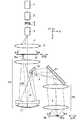
本発明の一実施例を図面によって説明する。図1は本発明による投影露光装置の概略図を示す。レーザー光源1より発した直線偏光は、整形光学系2によってその光束形状を整形された後に、複屈折光学部材によって形成された偏角プリズム3と、等方性材料によって形成された等方性プリズム4とを通過し、オプティカルインテグレータ5によって複数の光源像を形成し、コンデンサー6を介してレチクルRをケーラー照明する。以上のようにこの露光装置の照明光学系は、レーザー光源1からコンデンサー6までに至る上記各光学部材によって構成されている。
【0011】
レチクルRの下面には回路パターンが描かれており、このパターンを透過した光束は第1結像光学系10によってパターンの中間像15を形成する。第1結像光学系10には1つの凹面鏡11が配置されており、したがって第1結像光学系は部分的に往復光学系となっている。中間像15の近傍には第1平面鏡16が配置されており、同平面鏡16によって、凹面鏡11に向う光束と、凹面鏡11から反射した光束とが分離されている。
【0012】
第1平面鏡16によって光路を90°偏向された光束は、第2平面鏡21によって更に光路を90°偏向されており、これにより、第1光学系10と平行な光路に戻っている。第2平面鏡21によって90°偏向された光路には第2結像光学系20が配置されており、同光学系20によって中間像15の再結像が形成され、この再結像の位置に、ウエハWの感光面が配置されている。以上のようにこの露光装置の投影光学系は、第1結像光学系10から第2結像光学系に至る上記各光学部材によって構成されている。
なお、本実施例では第1平面鏡16と第2結像光学系20との間に第2平面鏡21を配置したが、第1平面鏡に引き続いて第2結像光学系20を配置し、同光学系20の内部に第2平面鏡21を配置する構成とすることもできる。
【0013】
図2(A)は図1中A−A線矢視図を示し、同図中、Raは照明光学系による照明領域を示し、Rbは投影光学系の物体面上有効領域を示す。また図2(B)は図1中B−B線矢視図を示し、同図中、Waは投影光学系による露光領域を示し、Wbは投影光学系の像面上有効領域を示す。本実施例の投影光学系は、第1結像光学系10の内部に往復光学系を持っているから、光軸zを使用することはできない。それ故照明領域Ra及び露光領域Waは、光軸zを含まない長方形の形状となっている。
【0014】
そしてレチクルRとウエハWとは、照明領域Ra及び露光領域Waの短手方向に、投影光学系の倍率に比例した速度比にて、同期して走査するように構成されている。こうして照明領域Ra及び露光領域Waを、その短手方向に拡大した範囲のパターンが、ウエハWの感光面上に投影露光される。
なお第1結像光学系10の倍率はほぼ等倍であり、第2結像光学系20の倍率は縮小倍率であり、したがって投影光学系全体の倍率は縮小倍率である。
また本実施例では照明領域Ra及び露光領域Waの形状を長方形状としているが、照明領域Ra及び露光領域Waの形状は、任意の直線ないしは曲線を走査方向に移動したときに塗りつぶされる形状とすることができ、例えば円弧を、弦の2等分方向に移動したときに塗りつぶされる形状とすることもできる。
【0015】
ここで、第1結像光学系10の光軸z方向をZ方向とし、Z方向と直交し互いに直交する2方向をX及びY方向とし、このうち図1の紙面内にX方向をとり、図1の紙面と直交する方向にY方向をとる。図1に示すように、第1平面鏡16も第2平面鏡21も、XY面をY軸周りに45°回転した位置に配置されている。
【0016】
次に図3(A)は、偏角プリズム3と等方性プリズム4との拡大図を示し、図3(B)、(C)及び(D)は、それぞれ図3(A)中、B−B線、C−C線及びD−D線矢視図を示す。図3(A)と(C)に示すように、偏角プリズム3の入射面はXY面に配置されており、射出面はXY面をY軸周りに回転した位置に配置されている。また偏角プリズム3の光学軸3aは、X方向に配置されている。他方、等方性プリズム4の入射面はXY面をY軸周りに回転した位置に配置されており、射出面はXY面に配置されている。
【0017】
さて、レチクルRから発した各種の光線のうち、主光線CRはXZ面内にある。したがって以降、XZ面内を進行する光線について説明する。XZ面内を進行する光線のうちで振動面がXZ面内にある直線偏光は、第1平面鏡16に関しても第2平面鏡21に関しても、また、偏角プリズム3に関しても等方性プリズム4に関しても、P偏光である。同様に、XZ面内を進行する光線のうちで振動面がY方向と平行な直線偏光は、第1平面鏡16、第2平面鏡21、偏角プリズム3及び等方性プリズム4に関してS偏光である。
【0018】
図3(B)に示すように、偏角プリズム3に入射する光線のうち、XZ面内を進行する光線は、P偏光成分とS偏光成分とを含み、且つP偏光成分の方が多くなるように構成されている。この構成は、レーザー光源1の光軸周りの配置位置を調整することにより、あるいは、例えば偏角プリズム3の直前に1/2波長板を配置して、その光軸周りの配置位置を調整することによって達成される。
なお図3(B)では、XZ面内を進行して偏角プリズム3に入射する光線が直線偏光である場合を示しているが、P偏光成分の方が多い楕円偏光であっても良い。
【0019】
偏角プリズム3に垂直入射した光線のうちのS偏光成分(振動面がY方向と平行な偏光成分)は、電気ベクトルの振動方向が偏角プリズム3の光学軸3aと直交しているから、常光線oとして偏角プリズム3の内部を進む。他方P偏光成分(振動面がXZ面内にある偏光成分)は、電気ベクトルの振動方向が光学軸3aと平行であるから、異常光線eとして偏角プリズム3の内部を進む。但し両偏光成分o(S)、e(P)とも、偏角プリズム3の入射面に垂直入射しており、且つ、偏角プリズム3の光学軸3aがX方向に配置されているために、両成分は偏角プリズム3の内部を垂直に進む。
【0020】
その後両偏光成分o(S)、e(P)は、偏角プリズム3の射出面に達して屈折して射出する。その際、偏角プリズム3の素材が水晶のように正結晶であるとすると、常光線o(S偏光成分)の屈折率は、異常光線e(P偏光成分)の屈折率よりも小さいから、両成分は分岐して偏角プリズム3の射出面より射出する。その後両成分は、等方性プリズム4を通過することによって、分岐方向がZ方向に関して対称となるように変換される。
こうして等方性プリズム4射出後の光線は、図3(D)に示すように、P偏向成分とS偏向成分とに分離され、しかもP偏向成分の強度の方が強い光線となる。
【0021】
なお、XZ面内を進行して偏角プリズム3に入射する光線のうち、偏角プリズム3に垂直入射しない光線は、偏角プリズム3の入射面から、常光線o(S偏光成分)と異常光線e(P偏光成分)に分離する。また、偏角プリズム3は、常光線o(S偏光成分)と異常光線e(P偏光成分)との射出方向が異なるように分離するものである。したがって入射面が、XY面をY軸周りに回転した位置に配置され、射出面が、XY面に配置される構成としても良いし、入射面、射出面とも、XY面をY軸周りに回転した位置に配置してもよい。すなわち入射面と射出面との交線(稜線)がY方向にあれば良い。また、偏角プリズム3の光学軸3aは必ずしもX方向である必要はなく、XZ面内にあれば良い。但しZ方向と一致する場合は除く。また、等方性プリズム4は、偏角プリズム3にZ方向より入射した後に分岐して射出する常光線o(S偏光成分)と異常光線e(P偏光成分)を、Z軸対称に変換するものであるから、偏角プリズム3と同様に、入射面と射出面との交線(稜線)がY方向にあれば良い。
【0022】
P偏光とS偏光とに分離された光線は、レチクルRを照明し、投影光学系を介してレチクルパターンの像をウエハW上に投影する。その際、投影光学系の第1及び第2平面鏡16、21にて反射することにより、P偏光の強度は相対的に低下する。図3(B)に示した偏角プリズム3に入射する光の偏光状態は、2回の反射によってP偏光の強度が相対的に低下したときに、P偏光の強度とS偏光の強度がほぼ等しくなるように設定されている。
【0023】
すなわち本実施例では投影光学系に2つの平面鏡16、21が配置されているから、図3(D)に示す等方性プリズム4射出後の光の偏光度は、前記した(1)式の値の2乗とすれば良く、その偏光度を持つ部分偏光となるように、偏角プリズム3に入射する光の偏光状態を調節している。
これにより、ウエハWは等しい強度のP偏光とS偏光とによって、すなわち完全非偏光の光によって露光されるから、偏光状態による露光むらを解消することができる。
【0024】
第1平面鏡16と第2平面鏡21に用いる反射膜については、P偏光に対する反射率RpとS偏光に対する反射率Rsとの差ΔRの、それぞれの平面鏡16、21に入射するすべての光線についての最大値ΔRmaxと最小値ΔRminとの差ΔRmax−ΔRminが、
ΔRmax−ΔRmin≦0.1
となるように形成することが好ましい。これにより、瞳面内及び露光領域内(視野内)の偏光度の差を小さくすることができ、露光領域全域でレチクルパターンの方向性に依存しない0.1ミクロン単位の解像度を実現することができる。
【0025】
以上説明のように、縮小投影光学系の場合、ウエハW側の開口数の方がレチクルR側に比べて大きく、偏光の方向性の影響ははるかに大きい。したがってレチクルRを上記の如き部分偏光で照明することにより、ウエハW上には偏光度の小さい光が到達することとなり、レチクルパターンの方向性に依存しない0.1ミクロン単位の解像度を実現している。
【0026】
更に、投影光学系が光軸zを含まないスリット状もしくは円弧状の照明・露光領域Ra、Waを用い、レチクルRとウエハWを同時に走査して大きな露光領域Waを得る走査光学系で、レチクルパターンの中間像15を形成する第1結像光学系10と、中間像15の再結像をウエハWの感光面上に形成する第2結像光学系20から構成され、中間像15付近に配置された光軸を偏向するための平面鏡16を用いることで、透過反射面をもつ偏光ビームスプリッタ等の製造困難な光路変換部材を用いずに、製造が容易で高いスループットを持った投影露光装置を実現できる。
【0027】
また、平面鏡15が第1結像光学系10から第2結像光学系20へ至る光路中に配置され、投影光学系中に少なくとも1つ凹面反射鏡11を用いることで、像側で大きな開口数を持ちつつ、投影光学系の小型化を達成することが可能で、現実的な大きさの投影露光装置となる。
【0028】
更に、第1結像光学系10中に凹面反射鏡11を採用し、第2結像光学系20が縮小の結像倍率を有することで、像側で大きな開口数を達成することが可能で、高い解像力を持つ投影露光装置が実現される。
また、中間像付近に配置した第1平面鏡15のほかに、第1平面鏡15とウエハWとの間の光路中に第2平面鏡21を配置することで、レチクルRのパターン面とウエハWの感光面とを平行にすることが可能で、レチクルステージ及びウエハステージが受ける重力の影響を、走査方向と垂直にすることができ、安定した走査露光が実現できる。
【0029】
【発明の効果】
以上説明のように、光線を偏向する平面鏡は、P偏光に対する反射率とS偏光に対する反射率とが異なるが、本発明では1または複数個の平面鏡で反射した後のP偏光の強度とS偏光の強度とが等しくなるようにすることができるから、ウエハを完全非偏光あるいはそれに近い光で露光することができ、偏光状態に起因する露光むらを解消することができる。
【図面の簡単な説明】
【図1】本発明による投影露光装置の一実施例を示す概略図
【図2】図1中(A)A−A線矢視図と、(B)B−B線矢視図
【図3】(A)偏角プリズムと等方性プリズムを示す側面図と、図A中(B)B−B線矢視図、(C)C−C線矢視図、及び(D)D−D線矢視図
【符号の説明】
1…レーザー光源 2…整形光学系
3…偏角プリズム 4…等方性プリズム
5…オプティカルインテグレータ 6…コンデンサー
10…第1結像光学系 11…凹面鏡
15…中間像 16…第1平面鏡
20…第2結像光学系 21…第2平面鏡
R…レチクル W…ウエハ
Ra…照明領域 Wa…露光領域[0001]
BACKGROUND OF THE INVENTION
The present invention relates to a projection exposure apparatus used when, for example, a semiconductor element, a liquid crystal display element or the like is manufactured in a photolithography process. In particular, by using a reflection system as an element of a projection optical system, the present invention relates to a projection exposure apparatus. The present invention relates to a projection exposure apparatus including a catadioptric projection optical system having a resolution of 1 micron unit.
[0002]
[Prior art]
In a photolithography process for manufacturing a semiconductor element or the like, an image of a pattern on a photomask or a reticle (hereinafter, collectively referred to as a reticle) is transferred to a wafer coated with a photoresist or the like via a projection optical system. A projection exposure apparatus that exposes a glass plate or the like (hereinafter collectively referred to as a wafer) is used. As the degree of integration of semiconductor elements and the like improves, the resolving power required for the projection optical system used in the projection exposure apparatus is increasing. In order to satisfy this requirement, it has become necessary to shorten the wavelength of the illumination light and increase the numerical aperture (NA) of the projection optical system.
[0003]
However, when the wavelength of illumination light is shortened, the types of glass materials that can be practically used due to light absorption are limited. When the wavelength is 300 nm or less, the only glass materials that can be used at present are synthetic quartz and fluorite. Since the Abbe numbers of the two are not far enough to correct chromatic aberration, it is difficult to correct chromatic aberration.
Further, since the required optical performance is extremely high, it is necessary to make each aberration almost no aberration. In order to achieve this with a refractive optical system composed only of lens groups, a large number of lenses are required, and it is inevitable to reduce the transmittance and increase the cost for manufacturing the optical system.
[0004]
On the other hand, a reflective optical system using a power such as a concave mirror has no chromatic aberration and shows a contribution to the Petzval sum opposite to that of a lens, so a so-called catadioptric optical system combining a reflective optical system and a refractive optical system. According to this, various aberrations including chromatic aberration can be made almost non-aberration without increasing the number of lenses. Various techniques for forming a projection optical system using such a catadioptric optical system have been proposed. Among them, as a type that forms an intermediate image once in the middle of an optical system, JP-A-63-163319, JP-B7-111512, JP-B-5-25170, USP-4,779 966, etc. are disclosed.
[0005]
[Problems to be solved by the invention]
In the prior art as described above, a spherical mirror such as a concave mirror is always used for aberration correction. Therefore, it is necessary to separate the optical path of the light from the reticle toward the spherical mirror and the optical path of the reflected light returning from the spherical mirror, and to deflect the optical path of the reflected light returning from the spherical mirror toward the wafer. Therefore, one or more plane mirrors coated with a reflective film are required. However, a plane mirror that deflects a light beam has different reflectivity for P-polarized light and reflectivity for S-polarized light.
In particular, when the exposure wavelength is shortened, the difference in reflectance between the P-polarized light and the S-polarized light due to the reflective film increases due to a decrease in the film material, and as a result, polarized light with directionality is generated. When polarized light having directionality is used for projection exposure, the imaging performance changes depending on the directionality of the reticle pattern. The amount of change in imaging performance is proportional to the numerical aperture, and a normal projection optical system has a reduction magnification, and therefore has a larger numerical aperture on the wafer side. Therefore, in this case, the change in imaging performance on the wafer becomes remarkable, which becomes a big problem in the photolithography process.
In view of this, the present invention achieves a large numerical aperture in the ultraviolet wavelength range, the optical system is a practical size, and does not depend on the direction of the reticle pattern, and has a resolution of 0.1 micron. It is an object of the present invention to provide a projection exposure apparatus including a mold projection optical system.
[0006]
[Means for Solving the Problems]
In order to achieve the above object, the present invention includes an illumination optical system that illuminates a pattern formed on a projection original plate, one or more spherical mirrors, a plurality of lenses, and one or more plane mirrors, In a projection exposure apparatus comprising a catadioptric projection optical system that forms an image of a pattern on a photosensitive surface of an object to be exposed, the illumination optical systemtransmits light from the catadioptric projection optical system toward the photosensitive surface. In order to make the polarization state substantially non-polarized , the projection exposure apparatus is configured to illuminate the pattern with partially polarized light.
The present invention also provides a projection exposure apparatus that forms an image of a predetermined pattern on a photosensitive surface of an object to be exposed based on light from a light source, and is in an optical path between the light source and the object to be exposed. And a plane mirror for deflecting incident light, and a degree of polarization control means for controlling the degree of polarization of the incident light incident on the plane mirrorso as to expose the photosensitive surface substantially unpolarized light. A characteristic projection exposure apparatus was obtained.
The present invention is also a method for adjusting a projection exposure apparatus that forms an image of a predetermined pattern on a photosensitive surface of an object to be exposed based on light from a light source, wherein the projection exposure apparatus includes the light source and the light source. Located in the optical path between the object to be exposed and equipped with a plane mirror that deflects the incident light, the degree of polarization of the incident light incident on the plane mirror is adjustedso that the light reaching the photosensitive surface is almost unpolarized Then, the projection exposure apparatus adjustment method is characterized in that the degree of polarization of the reflected light reflected by the plane mirror is made smaller than the degree of polarization of the incident light.
[0007]
DETAILED DESCRIPTION OF THE INVENTION
When the light incident on the plane mirror consists only of P-polarized light and S-polarized light, and both polarized lights are not synthesized, that is, does not include circularly polarized light, elliptically polarized light, or linearly polarized light that vibrates in directions other than the P-polarized light direction and S-polarized light direction In this case, the Stokes parameters S0 to S3 of the incident light are
S0 = Is + Ip
S1 = Is −Ip
S2 = 0
S3 = 0
Is , Ip : the intensity of the S-polarized component of the incident light and the intensity of the P-polarized component.
Therefore, in this case, the polarization degree V of the incident light is
[0008]
On the other hand, the intensity of the reflected light reflected by the plane mirror is
Is ′ = Is · Rs
Ip ′ = Ip · Rp
Is ′, Ip ′: the intensity of the S-polarized component of the reflected light, the intensity of the P-polarized component Rs , Rp : the intensity reflectance for S-polarized light, and the intensity reflectance for P-polarized light.
Therefore, the Stokes parameters S0 ′ to S3 ′ of the reflected light and the degree of polarization V ′ of the reflected light are
S 0 '= I s' + I p' = I s · R s + I p · R p
S 1 '= I s' -I p' = I s · R s -I p · R p
S2 ′ = 0
S3 ′ = 0
[0009]
Here, in order for the polarization degree of the reflected light to be V ′ = 0,
Is · Rs -Ip · Rp = 0
That is,
Is = Ip · Rp / Rs
Therefore, the polarization degree V of the incident light is
In general, since the intensity reflectances Rs and Rp are Rs > Rp ,
S 1 = I s -I p = I p / R s · (R p -R s) <0
Which represents the polarization in the P direction. Accordingly, when a partially polarized light having a polarization degree of | (Rp −Rs ) / (Rp + Rs ) | is incident on the plane mirror in the P direction, the polarization degree V ′ of the reflected light becomes V ′ = 0. Reflected light that is completely unpolarized can be obtained.
[0010]
【Example】
An embodiment of the present invention will be described with reference to the drawings. FIG. 1 shows a schematic view of a projection exposure apparatus according to the present invention. The linearly polarized light emitted from the laser light source 1 is shaped by the shaping
[0011]
A circuit pattern is drawn on the lower surface of the reticle R, and the light beam that has passed through this pattern forms an
[0012]
The light beam whose optical path is deflected by 90 ° by the
In the present embodiment, the
[0013]
FIG. 2A shows an AA arrow view in FIG. 1, in which Ra indicates an illumination area by the illumination optical system, and Rb indicates an effective area on the object plane of the projection optical system. 2B is a view taken along the line BB in FIG. 1. In FIG. 2, Wa represents an exposure area by the projection optical system, and Wb represents an effective area on the image plane of the projection optical system. Since the projection optical system of the present embodiment has a reciprocating optical system inside the first imaging
[0014]
The reticle R and the wafer W are configured to scan synchronously in the lateral direction of the illumination area Ra and the exposure area Wa at a speed ratio proportional to the magnification of the projection optical system. In this way, a pattern in a range in which the illumination area Ra and the exposure area Wa are enlarged in the lateral direction is projected and exposed on the photosensitive surface of the wafer W.
Note that the magnification of the first imaging
In this embodiment, the illumination area Ra and the exposure area Wa are rectangular. However, the illumination area Ra and the exposure area Wa are shaped so as to be filled when an arbitrary straight line or curve is moved in the scanning direction. For example, the arc may be a shape that is filled when the chord is moved in the bisecting direction.
[0015]
Here, the optical axis z direction of the first imaging
[0016]
Next, FIG. 3A shows an enlarged view of the
[0017]
Of the various rays emitted from the reticle R, the principal ray CR is in the XZ plane. Therefore, hereinafter, light rays traveling in the XZ plane will be described. Of the light rays traveling in the XZ plane, the linearly polarized light whose vibration plane is in the XZ plane is related to the
[0018]
As shown in FIG. 3B, among the light rays incident on the
FIG. 3B shows a case where the light beam that travels in the XZ plane and enters the
[0019]
The S-polarized component (polarized component whose vibration plane is parallel to the Y direction) of the light beam perpendicularly incident on the
[0020]
Thereafter, both polarization components o (S) and e (P) reach the exit surface of the
As shown in FIG. 3D, the light beam emitted from the
[0021]
Of the light rays that travel in the XZ plane and enter the
[0022]
The light beam separated into the P-polarized light and the S-polarized light illuminates the reticle R, and projects an image of the reticle pattern onto the wafer W via the projection optical system. At that time, the intensity of the P-polarized light is relatively lowered by being reflected by the first and second plane mirrors 16 and 21 of the projection optical system. The polarization state of the light incident on the
[0023]
That is, in this embodiment, since the two plane mirrors 16 and 21 are arranged in the projection optical system, the degree of polarization of light after exiting the
Thereby, since the wafer W is exposed by the P-polarized light and the S-polarized light having the same intensity, that is, by completely non-polarized light, uneven exposure due to the polarization state can be eliminated.
[0024]
With respect to the reflective films used for the
ΔRmax −ΔRmin ≦ 0.1
It is preferable to form such that Thereby, the difference in the degree of polarization in the pupil plane and in the exposure area (in the field of view) can be reduced, and a resolution of 0.1 micron unit independent of the directionality of the reticle pattern can be realized over the entire exposure area. it can.
[0025]
As described above, in the case of the reduction projection optical system, the numerical aperture on the wafer W side is larger than that on the reticle R side, and the influence of the directionality of polarization is much greater. Therefore, by illuminating the reticle R with the partial polarization as described above, light having a small degree of polarization reaches the wafer W, and a resolution of 0.1 micron unit independent of the directionality of the reticle pattern is realized. Yes.
[0026]
Further, the projection optical system uses a slit-shaped or arc-shaped illumination / exposure area Ra, Wa that does not include the optical axis z, and simultaneously scans the reticle R and the wafer W to obtain a large exposure area Wa. The first imaging
[0027]
Further, the
[0028]
Further, by adopting the concave reflecting
In addition to the
[0029]
【The invention's effect】
As described above, the plane mirror that deflects the light beam has different reflectance for P-polarized light and reflectance for S-polarized light. In the present invention, the intensity of P-polarized light and the S-polarized light after being reflected by one or more plane mirrors. Therefore, the wafer can be exposed to completely non-polarized light or light close thereto, and uneven exposure due to the polarization state can be eliminated.
[Brief description of the drawings]
FIG. 1 is a schematic view showing an embodiment of a projection exposure apparatus according to the present invention. FIG. 2 is a view taken along line AA in FIG. 1 and a view taken along line B-B in FIG. (A) Side view showing declination prism and isotropic prism, (B) view taken along line B-B, (C) view taken along line C-C, and (D) DD in FIG. Arrow view [Explanation of symbols]
DESCRIPTION OF SYMBOLS 1 ... Laser
Claims (13)
Translated fromJapanese前記照明光学系は、前記反射屈折型投影光学系から前記感光面へ向かう光の偏光状態をほぼ非偏光にするために、前記パターンを部分偏光光によって照明するように構成されたことを特徴とする投影露光装置。A catadioptric projection having an illumination optical system for illuminating a predetermined pattern, one or more spherical mirrors, a plurality of lenses, and one or more plane mirrors, and forming an image of the pattern on a photosensitive surface of an object to be exposed In a projection exposure apparatus comprising an optical system,
The illumination optical system is configured to illuminate the pattern with partially polarized lightin order to make the polarization state of light traveling from the catadioptric projection optical system toward the photosensitive surface substantially non-polarized light. Projection exposure apparatus.
前記投影原版と被露光物体とは、前記照明領域及び露光領域の短手方向に同期して走査するように配置され、
前記投影光学系は、前記投影光学系に配置されたいずれか1つの前記平面鏡の近傍に前記パターンの中間像を形成する第1結像光学系と、前記中間像の再結像を前記感光面上に形成する第2結像光学系とを有することを特徴とする請求項1、2又は3記載の投影露光装置。The illumination area where the illumination optical system illuminates the pattern and the exposure area formed by the projection optical system on the photosensitive surface are formed in a slit shape or an arc shape,
The projection original plate and the object to be exposed are arranged to scan in synchronization with the short direction of the illumination area and the exposure area,
The projection optical system includes: a first imaging optical system that forms an intermediate image of the pattern in the vicinity of any one of the plane mirrors disposed in the projection optical system; and a reimaging of the intermediate image on the photosensitive surface 4. The projection exposure apparatus according to claim 1, further comprising a second imaging optical system formed on the projection imaging system.
前記光源と前記被露光物体との間の光路中に配置されて、入射光を偏向する平面鏡と、
前記感光面をほぼ非偏光で露光するように、前記平面鏡へ入射する入射光の偏光度を制御する偏光度制御手段とを備えていることを特徴とする投影露光装置。In a projection exposure apparatus that forms an image of a predetermined pattern on a photosensitive surface of an object to be exposed based on light from a light source,
A plane mirror disposed in an optical path between the light source and the object to be exposed to deflect incident light;
A projection exposure apparatus, comprising: a degree of polarization control means for controlling a degree of polarization of incident light incident on the plane mirrorso that the photosensitive surface is exposed substantially unpolarized light .
前記偏光度制御手段は前記複屈折光学部材への入射光の偏光度を制御していることを特徴とする請求項7又は8記載の投影露光装置。A birefringent optical member disposed in an optical path between the polarization degree control means and the pattern;
9. The projection exposure apparatus according to claim 7, wherein the degree of polarization control means controls the degree of polarization of incident light on the birefringent optical member.
請求項1乃至9のいずれか1項記載の投影露光装置を用いて前記パターンの像を前記被露光物体の前記感光面上に形成していることを特徴とする投影露光方法。In a projection exposure method for projecting an image of a predetermined pattern onto a photosensitive surface of an object to be exposed,
10. A projection exposure method, wherein an image of the pattern is formed on the photosensitive surface of the object to be exposed using the projection exposure apparatus according to any one of claims 1 to 9.
前記投影露光装置は、前記光源と前記被露光物体との間の光路中に配置されて、入射光を偏向する平面鏡を備え、
前記感光面に達する光がほぼ非偏光となるように、前記平面鏡へ入射する入射光の偏光度を調整して、前記平面鏡で反射された反射光の偏光度を、前記入射光の偏光度よりも小さくすることを特徴とする投影露光装置の調整方法。A method for adjusting a projection exposure apparatus that forms an image of a predetermined pattern on a photosensitive surface of an object to be exposed based on light from a light source,
The projection exposure apparatus includes a plane mirror disposed in an optical path between the light source and the object to be exposed and deflecting incident light.
The degree of polarization of incident light incident on the plane mirror is adjustedso that the light reaching the photosensitive surface is substantially unpolarized, and the degree of polarization of reflected light reflected by the plane mirror is determined from the degree of polarization of the incident light. And adjusting the projection exposure apparatus.
前記光源の光軸廻りの配置位置を調整することを特徴とする請求項11記載の調整方法。The projection exposure apparatus further includes a birefringent optical member disposed in an optical path from the light source to the pattern,
The adjustment method according to claim 11, wherein an arrangement position of the light source around the optical axis is adjusted.
前記波長板の光軸廻りの配置位置を調整することを特徴とする請求項11記載の調整方法。The projection exposure apparatus further includes a birefringent optical member disposed in an optical path from the light source to the pattern, and a wave plate disposed in an optical path between the birefringent optical member and the light source,
The adjusting method according to claim 11, wherein an arrangement position of the wave plate around the optical axis is adjusted.
Priority Applications (6)
| Application Number | Priority Date | Filing Date | Title |
|---|---|---|---|
| JP18149898AJP3985346B2 (en) | 1998-06-12 | 1998-06-12 | Projection exposure apparatus, projection exposure apparatus adjustment method, and projection exposure method |
| EP99111428AEP0964282B1 (en) | 1998-06-12 | 1999-06-11 | Projection exposure apparatus with a catadioptric projection optical system |
| DE69923376TDE69923376T2 (en) | 1998-06-12 | 1999-06-11 | Exposure projection apparatus with a catadioptric optical exposure system |
| US09/330,442US6466303B1 (en) | 1998-06-12 | 1999-06-11 | Projection exposure apparatus with a catadioptric projection optical system |
| AT99111428TATE288088T1 (en) | 1998-06-12 | 1999-06-11 | PROJECTION EXPOSURE DEVICE WITH CATADIOPTRIC PROJECTION SYSTEM |
| US10/226,347US6661499B2 (en) | 1998-06-12 | 2002-08-23 | Projection exposure apparatus with a catadioptric projection optical system |
Applications Claiming Priority (1)
| Application Number | Priority Date | Filing Date | Title |
|---|---|---|---|
| JP18149898AJP3985346B2 (en) | 1998-06-12 | 1998-06-12 | Projection exposure apparatus, projection exposure apparatus adjustment method, and projection exposure method |
Publications (3)
| Publication Number | Publication Date |
|---|---|
| JP2000003852A JP2000003852A (en) | 2000-01-07 |
| JP2000003852A5 JP2000003852A5 (en) | 2006-07-20 |
| JP3985346B2true JP3985346B2 (en) | 2007-10-03 |
Family
ID=16101820
Family Applications (1)
| Application Number | Title | Priority Date | Filing Date |
|---|---|---|---|
| JP18149898AExpired - LifetimeJP3985346B2 (en) | 1998-06-12 | 1998-06-12 | Projection exposure apparatus, projection exposure apparatus adjustment method, and projection exposure method |
Country Status (5)
| Country | Link |
|---|---|
| US (2) | US6466303B1 (en) |
| EP (1) | EP0964282B1 (en) |
| JP (1) | JP3985346B2 (en) |
| AT (1) | ATE288088T1 (en) |
| DE (1) | DE69923376T2 (en) |
Families Citing this family (41)
| Publication number | Priority date | Publication date | Assignee | Title |
|---|---|---|---|---|
| US7301605B2 (en)* | 2000-03-03 | 2007-11-27 | Nikon Corporation | Projection exposure apparatus and method, catadioptric optical system and manufacturing method of devices |
| DE10010131A1 (en)* | 2000-03-03 | 2001-09-06 | Zeiss Carl | Microlithography projection exposure with tangential polarization involves using light with preferred direction of polarization oriented perpendicularly with respect to plane of incidence |
| JP3927753B2 (en)* | 2000-03-31 | 2007-06-13 | キヤノン株式会社 | Exposure apparatus and device manufacturing method |
| DE10016176A1 (en) | 2000-03-31 | 2001-10-04 | Zeiss Carl | Microlithographic illumination system, has optical element that can detect entire light beam with continuously differentiable surface in near field and asymmetrical with respect to optical axis |
| DE10124566A1 (en)* | 2001-05-15 | 2002-11-21 | Zeiss Carl | Optical imaging system with polarizing agents and quartz crystal plate therefor |
| US7031069B2 (en) | 2001-05-19 | 2006-04-18 | Carl Zeiss Smt Ag | Microlithographic illumination method and a projection lens for carrying out the method |
| DE10124474A1 (en)* | 2001-05-19 | 2002-11-21 | Zeiss Carl | Microlithographic exposure involves compensating path difference by controlled variation of first and/or second optical paths; image plane difference is essentially independent of incident angle |
| JP3826047B2 (en) | 2002-02-13 | 2006-09-27 | キヤノン株式会社 | Exposure apparatus, exposure method, and device manufacturing method using the same |
| US20050190446A1 (en)* | 2002-06-25 | 2005-09-01 | Carl Zeiss Amt Ag | Catadioptric reduction objective |
| US6922293B2 (en)* | 2002-07-02 | 2005-07-26 | Nikon Corporation | Kinematic optical mounting assembly with flexures |
| DE10240598A1 (en)* | 2002-08-27 | 2004-03-25 | Carl Zeiss Smt Ag | Catadioptric reflective/reduction lens for mapping an image pattern transfers a picture of the pattern in an object plane into an image plane |
| TW200412617A (en)* | 2002-12-03 | 2004-07-16 | Nikon Corp | Optical illumination device, method for adjusting optical illumination device, exposure device and exposure method |
| KR101547077B1 (en) | 2003-04-09 | 2015-08-25 | 가부시키가이샤 니콘 | Exposure method and apparatus, and device manufacturing method |
| US7423343B2 (en)* | 2003-08-05 | 2008-09-09 | Semiconductor Energy Laboratory Co., Ltd. | Wiring board, manufacturing method thereof, semiconductor device and manufacturing method thereof |
| DE10338983A1 (en) | 2003-08-20 | 2005-03-17 | Carl Zeiss Smt Ag | Projection lens for microlithography scans a pattern set up in a projection lens object plane into a projection lens focal plane |
| US7408616B2 (en) | 2003-09-26 | 2008-08-05 | Carl Zeiss Smt Ag | Microlithographic exposure method as well as a projection exposure system for carrying out the method |
| TWI573175B (en)* | 2003-10-28 | 2017-03-01 | 尼康股份有限公司 | Optical illumination device, exposure device, exposure method and device manufacturing method |
| JP2005136244A (en)* | 2003-10-31 | 2005-05-26 | Semiconductor Leading Edge Technologies Inc | Exposure method |
| TWI385414B (en) | 2003-11-20 | 2013-02-11 | 尼康股份有限公司 | Optical illuminating apparatus, illuminating method, exposure apparatus, exposure method and device fabricating method |
| KR101165862B1 (en) | 2004-01-16 | 2012-07-17 | 칼 짜이스 에스엠티 게엠베하 | Polarization-modulating optical element |
| US20070019179A1 (en) | 2004-01-16 | 2007-01-25 | Damian Fiolka | Polarization-modulating optical element |
| US8270077B2 (en) | 2004-01-16 | 2012-09-18 | Carl Zeiss Smt Gmbh | Polarization-modulating optical element |
| TWI389174B (en) | 2004-02-06 | 2013-03-11 | 尼康股份有限公司 | Polarization changing device, optical illumination apparatus, light-exposure apparatus and light-exposure method |
| DE102004010569A1 (en)* | 2004-02-26 | 2005-09-15 | Carl Zeiss Smt Ag | Illumination system for a microlithography projection exposure apparatus |
| JP4497968B2 (en)* | 2004-03-18 | 2010-07-07 | キヤノン株式会社 | Illumination apparatus, exposure apparatus, and device manufacturing method |
| JP4776891B2 (en) | 2004-04-23 | 2011-09-21 | キヤノン株式会社 | Illumination optical system, exposure apparatus, and device manufacturing method |
| US7242456B2 (en)* | 2004-05-26 | 2007-07-10 | Asml Holdings N.V. | System and method utilizing a lithography tool having modular illumination, pattern generator, and projection optics portions |
| JP2006173305A (en)* | 2004-12-15 | 2006-06-29 | Canon Inc | Exposure apparatus and method, and device manufacturing method |
| US7349068B2 (en)* | 2004-12-17 | 2008-03-25 | Asml Netherlands B.V. | Lithographic apparatus and device manufacturing method |
| WO2006084479A1 (en)* | 2005-02-12 | 2006-08-17 | Carl Zeiss Smt Ag | Microlithographic projection exposure apparatus |
| DE102005031084A1 (en)* | 2005-06-28 | 2007-01-04 | Carl Zeiss Smt Ag | Microlithographic exposure method and projection exposure apparatus for carrying out the method |
| DE102006031807A1 (en)* | 2005-07-12 | 2007-01-18 | Carl Zeiss Smt Ag | Lighting device for microlithographic projection exposure system, has depolarizing system to effect polarization direction variation such that light mixer produces light without preferred direction, and including plates of crystal material |
| WO2007020004A1 (en) | 2005-08-17 | 2007-02-22 | Carl Zeiss Smt Ag | Projection objective and method for optimizing a system diaphragm of a projection objective |
| US20070091452A1 (en)* | 2005-10-25 | 2007-04-26 | Scott Lerner | Projection system and method |
| US7649676B2 (en)* | 2006-06-14 | 2010-01-19 | Asml Netherlands B.V. | System and method to form unpolarized light |
| DE102006032878A1 (en)* | 2006-07-15 | 2008-01-17 | Carl Zeiss Smt Ag | Illumination system of a microlithographic projection exposure apparatus |
| US7817250B2 (en) | 2007-07-18 | 2010-10-19 | Carl Zeiss Smt Ag | Microlithographic projection exposure apparatus |
| DE102008041179B4 (en) | 2008-08-12 | 2010-11-04 | Carl Zeiss Smt Ag | Illumination optics for a microlithography projection exposure apparatus |
| JP2009065175A (en)* | 2008-10-02 | 2009-03-26 | Canon Inc | Illumination optics |
| DE102011084637A1 (en) | 2011-10-17 | 2013-04-18 | Carl Zeiss Smt Gmbh | Microlithographic exposure method, as well as illumination device |
| CN104950584B (en)* | 2014-03-25 | 2018-01-30 | 上海微电子装备(集团)股份有限公司 | Imaging is to Barebone |
Family Cites Families (56)
| Publication number | Priority date | Publication date | Assignee | Title |
|---|---|---|---|---|
| US3917399A (en)* | 1974-10-02 | 1975-11-04 | Tropel | Catadioptric projection printer |
| JPS6051687B2 (en) | 1975-09-26 | 1985-11-15 | 株式会社ニコン | Depolarization device in optical system with analyzer |
| US4295103A (en) | 1978-03-23 | 1981-10-13 | Ariold Ljudmirsky | Metal vapor laser |
| US4334199A (en) | 1978-10-27 | 1982-06-08 | The University Of Rochester | Excimer laser |
| JPS561058A (en) | 1979-06-18 | 1981-01-08 | Matsushita Electric Ind Co Ltd | Exposure method |
| JPS5878481A (en) | 1981-11-04 | 1983-05-12 | Kimmon Electric Co Ltd | Metal vapor laser |
| US4799791A (en) | 1984-02-13 | 1989-01-24 | Canon Kabushiki Kaisha | Illuminance distribution measuring system |
| JPS6147524A (en) | 1984-08-14 | 1986-03-08 | Olympus Optical Co Ltd | Spectrophotometer |
| JPH0652699B2 (en) | 1984-09-13 | 1994-07-06 | 株式会社ニコン | Exposure equipment |
| US4779966A (en) | 1984-12-21 | 1988-10-25 | The Perkin-Elmer Corporation | Single mirror projection optical system |
| JPS61156737A (en) | 1984-12-27 | 1986-07-16 | Canon Inc | Circuit manufacturing method and exposure equipment |
| JPS61202431A (en) | 1985-03-06 | 1986-09-08 | Canon Inc | Projection exposure apparatus |
| JPS61218132A (en) | 1985-03-25 | 1986-09-27 | Hitachi Ltd | Projection exposure apparatus |
| US4947030A (en) | 1985-05-22 | 1990-08-07 | Canon Kabushiki Kaisha | Illuminating optical device |
| US4769750A (en) | 1985-10-18 | 1988-09-06 | Nippon Kogaku K. K. | Illumination optical system |
| JPS62260118A (en) | 1986-05-02 | 1987-11-12 | Komatsu Ltd | Projection exposure device |
| JPS6332555A (en) | 1986-07-25 | 1988-02-12 | Nippon Telegr & Teleph Corp <Ntt> | Exposing device |
| US4939630A (en) | 1986-09-09 | 1990-07-03 | Nikon Corporation | Illumination optical apparatus |
| JPH0669015B2 (en) | 1986-09-11 | 1994-08-31 | キヤノン株式会社 | Projection exposure device |
| JPS6381882A (en) | 1986-09-25 | 1988-04-12 | Nikon Corp | Energy amount control device |
| JPH0781824B2 (en) | 1986-11-17 | 1995-09-06 | 株式会社ニコン | Alignment device |
| JPS63147273A (en) | 1986-12-11 | 1988-06-20 | Canon Inc | Method for detecting alignment pattern |
| US4747678A (en) | 1986-12-17 | 1988-05-31 | The Perkin-Elmer Corporation | Optical relay system with magnification |
| JPS63179519A (en) | 1987-01-21 | 1988-07-23 | Nikon Corp | semiconductor exposure equipment |
| JPS63197334A (en) | 1987-02-12 | 1988-08-16 | Canon Inc | lighting equipment |
| JPS63227082A (en) | 1987-03-17 | 1988-09-21 | Toshiba Corp | Gas laser oscillator |
| US4864123A (en) | 1987-05-08 | 1989-09-05 | Nikon Corporation | Apparatus for detecting the level of an object surface |
| JPH01119020A (en) | 1987-10-30 | 1989-05-11 | Canon Inc | exposure equipment |
| JP2636863B2 (en) | 1987-12-23 | 1997-07-30 | 株式会社ニコン | Polarizing device |
| US5307207A (en) | 1988-03-16 | 1994-04-26 | Nikon Corporation | Illuminating optical apparatus |
| JPH0237333A (en) | 1988-07-27 | 1990-02-07 | Olympus Optical Co Ltd | Finder equipped with polarization eliminating plate |
| US5253110A (en) | 1988-12-22 | 1993-10-12 | Nikon Corporation | Illumination optical arrangement |
| US5475491A (en) | 1989-02-10 | 1995-12-12 | Canon Kabushiki Kaisha | Exposure apparatus |
| JPH02232917A (en) | 1989-03-07 | 1990-09-14 | Toshiba Corp | Semiconductor exposing device and exposing method |
| JPH0350818A (en) | 1989-07-19 | 1991-03-05 | Canon Inc | exposure equipment |
| JP2913725B2 (en) | 1990-01-31 | 1999-06-28 | 株式会社ニコン | Exposure equipment |
| US5052763A (en) | 1990-08-28 | 1991-10-01 | International Business Machines Corporation | Optical system with two subsystems separately correcting odd aberrations and together correcting even aberrations |
| US5541026A (en) | 1991-06-13 | 1996-07-30 | Nikon Corporation | Exposure apparatus and photo mask |
| JP2796005B2 (en)* | 1992-02-10 | 1998-09-10 | 三菱電機株式会社 | Projection exposure apparatus and polarizer |
| JPH05226222A (en) | 1992-02-13 | 1993-09-03 | Nikon Corp | Positioning device for exposure equipment |
| JPH05226224A (en) | 1992-02-17 | 1993-09-03 | Nikon Corp | Positioning device for exposure equipment |
| JP3747951B2 (en)* | 1994-11-07 | 2006-02-22 | 株式会社ニコン | Catadioptric optics |
| US5534970A (en)* | 1993-06-11 | 1996-07-09 | Nikon Corporation | Scanning exposure apparatus |
| KR0153796B1 (en)* | 1993-09-24 | 1998-11-16 | 사토 후미오 | Exposure apparatus and exposure method |
| DE19535392A1 (en) | 1995-09-23 | 1997-03-27 | Zeiss Carl Fa | Radial polarization-rotating optical arrangement and microlithography projection exposure system with it |
| JPH09167735A (en)* | 1995-12-15 | 1997-06-24 | Canon Inc | Projection exposure apparatus and semiconductor device manufacturing method using the same |
| DE19637563A1 (en) | 1996-09-14 | 1998-03-19 | Zeiss Carl Fa | Birefringent faceplate arrangement and DUV quarter-wave plate |
| JPH10153866A (en)* | 1996-11-22 | 1998-06-09 | Nikon Corp | Illumination device and exposure apparatus having the illumination device |
| KR100245414B1 (en) | 1997-06-26 | 2000-03-02 | 윤종용 | An illuminator system and an illuminating method of the same |
| DE19807120A1 (en) | 1998-02-20 | 1999-08-26 | Zeiss Carl Fa | Optical system with polarization compensator |
| DE19810089A1 (en) | 1998-03-10 | 1999-09-16 | Zeiss Carl Fa | Birefringent plate arrangement with stress birefringence |
| DE19829612A1 (en) | 1998-07-02 | 2000-01-05 | Zeiss Carl Fa | Microlithography lighting system with depolarizer |
| DE19851749A1 (en) | 1998-11-10 | 2000-05-11 | Zeiss Carl Fa | Polarization-optically compensated lens |
| DE19921795A1 (en) | 1999-05-11 | 2000-11-23 | Zeiss Carl Fa | Projection exposure system and exposure method of microlithography |
| DE10010131A1 (en) | 2000-03-03 | 2001-09-06 | Zeiss Carl | Microlithography projection exposure with tangential polarization involves using light with preferred direction of polarization oriented perpendicularly with respect to plane of incidence |
| DE10124474A1 (en) | 2001-05-19 | 2002-11-21 | Zeiss Carl | Microlithographic exposure involves compensating path difference by controlled variation of first and/or second optical paths; image plane difference is essentially independent of incident angle |
- 1998
- 1998-06-12JPJP18149898Apatent/JP3985346B2/ennot_activeExpired - Lifetime
- 1999
- 1999-06-11ATAT99111428Tpatent/ATE288088T1/ennot_activeIP Right Cessation
- 1999-06-11EPEP99111428Apatent/EP0964282B1/ennot_activeExpired - Lifetime
- 1999-06-11DEDE69923376Tpatent/DE69923376T2/ennot_activeExpired - Lifetime
- 1999-06-11USUS09/330,442patent/US6466303B1/ennot_activeExpired - Fee Related
- 2002
- 2002-08-23USUS10/226,347patent/US6661499B2/ennot_activeExpired - Lifetime
Also Published As
| Publication number | Publication date |
|---|---|
| US20030011756A1 (en) | 2003-01-16 |
| EP0964282A2 (en) | 1999-12-15 |
| US6466303B1 (en) | 2002-10-15 |
| US6661499B2 (en) | 2003-12-09 |
| JP2000003852A (en) | 2000-01-07 |
| DE69923376T2 (en) | 2006-03-30 |
| EP0964282B1 (en) | 2005-01-26 |
| EP0964282A3 (en) | 2000-05-10 |
| ATE288088T1 (en) | 2005-02-15 |
| DE69923376D1 (en) | 2005-03-03 |
Similar Documents
| Publication | Publication Date | Title |
|---|---|---|
| JP3985346B2 (en) | Projection exposure apparatus, projection exposure apparatus adjustment method, and projection exposure method | |
| USRE39024E1 (en) | Exposure apparatus having catadioptric projection optical system | |
| US5241423A (en) | High resolution reduction catadioptric relay lens | |
| US5289312A (en) | Catadioptric reduction projection optical system | |
| US5089913A (en) | High resolution reduction catadioptric relay lens | |
| JP2847883B2 (en) | Catadioptric reduction projection optical system | |
| USRE39296E1 (en) | Catadioptric projection systems | |
| JP4065923B2 (en) | Illumination apparatus, projection exposure apparatus including the illumination apparatus, projection exposure method using the illumination apparatus, and adjustment method of the projection exposure apparatus | |
| US6118596A (en) | Catadioptric reduction projection optical system and method | |
| EP1291695A2 (en) | Catadioptric optical reduction system with high numerical aperture | |
| JPH0862502A (en) | Catadioptric reduction projection optical system | |
| JP2003077827A (en) | Microlithographic illumination method and projection lens for carrying out the same | |
| US20020027718A1 (en) | Optical reduction system with elimination of reticle diffraction induced bias | |
| US6424471B1 (en) | Catadioptric objective with physical beam splitter | |
| JPH1048526A (en) | Objective lens of high resolving power and high intensity | |
| USRE38438E1 (en) | Catadioptric reduction projection optical system and exposure apparatus having the same | |
| JP2005311187A (en) | Illumination optical system, exposure apparatus, and device manufacturing method | |
| JP4236397B2 (en) | Reduction optical system | |
| US5251070A (en) | Catadioptric reduction projection optical system | |
| US7317583B2 (en) | High numerical aperture projection system and method for microlithography | |
| US20050207029A1 (en) | Catadioptric projection objective | |
| JP2005512151A (en) | Catadioptric reduction objective lens | |
| JP3852196B2 (en) | Projection optical system, projection exposure apparatus, and scanning projection exposure method | |
| JPH10308345A (en) | Catadioptric projection optics | |
| JP2003295062A (en) | Catadioptric imaging optics |
Legal Events
| Date | Code | Title | Description |
|---|---|---|---|
| A621 | Written request for application examination | Free format text:JAPANESE INTERMEDIATE CODE: A621 Effective date:20050607 | |
| RD05 | Notification of revocation of power of attorney | Free format text:JAPANESE INTERMEDIATE CODE: A7425 Effective date:20050811 | |
| A521 | Request for written amendment filed | Free format text:JAPANESE INTERMEDIATE CODE: A523 Effective date:20060602 | |
| A977 | Report on retrieval | Free format text:JAPANESE INTERMEDIATE CODE: A971007 Effective date:20061219 | |
| A131 | Notification of reasons for refusal | Free format text:JAPANESE INTERMEDIATE CODE: A131 Effective date:20070404 | |
| A521 | Request for written amendment filed | Free format text:JAPANESE INTERMEDIATE CODE: A523 Effective date:20070529 | |
| TRDD | Decision of grant or rejection written | ||
| A01 | Written decision to grant a patent or to grant a registration (utility model) | Free format text:JAPANESE INTERMEDIATE CODE: A01 Effective date:20070619 | |
| A61 | First payment of annual fees (during grant procedure) | Free format text:JAPANESE INTERMEDIATE CODE: A61 Effective date:20070702 | |
| R150 | Certificate of patent or registration of utility model | Free format text:JAPANESE INTERMEDIATE CODE: R150 | |
| FPAY | Renewal fee payment (event date is renewal date of database) | Free format text:PAYMENT UNTIL: 20100720 Year of fee payment:3 | |
| FPAY | Renewal fee payment (event date is renewal date of database) | Free format text:PAYMENT UNTIL: 20100720 Year of fee payment:3 | |
| FPAY | Renewal fee payment (event date is renewal date of database) | Free format text:PAYMENT UNTIL: 20180720 Year of fee payment:11 | |
| EXPY | Cancellation because of completion of term |