JP3983167B2 - Method for manufacturing metal oxide semiconductor field effect transistor - Google Patents
Method for manufacturing metal oxide semiconductor field effect transistorDownload PDFInfo
- Publication number
- JP3983167B2 JP3983167B2JP2002378306AJP2002378306AJP3983167B2JP 3983167 B2JP3983167 B2JP 3983167B2JP 2002378306 AJP2002378306 AJP 2002378306AJP 2002378306 AJP2002378306 AJP 2002378306AJP 3983167 B2JP3983167 B2JP 3983167B2
- Authority
- JP
- Japan
- Prior art keywords
- layer
- effect transistor
- field effect
- metal oxide
- trench
- Prior art date
- Legal status (The legal status is an assumption and is not a legal conclusion. Google has not performed a legal analysis and makes no representation as to the accuracy of the status listed.)
- Expired - Fee Related
Links
Images


Landscapes
- Electrodes Of Semiconductors (AREA)
- Thin Film Transistor (AREA)
- Insulated Gate Type Field-Effect Transistor (AREA)
Description
Translated fromJapanese【0001】
【発明の属する技術分野】
この発明は、半導体デバイス(Semiconductor Device)の構造とその製造方法に関し、特に、金属酸化膜半導体電界効果型トランジスター(MOSFET)とその製造方法に関する。
【0002】
【従来の技術】
金属酸化膜半導体(MOS)製造工程の線幅(Line-width)が日増しに縮小するにつれて、ソース(Source)およびドレイン(Drain)間のゲート(Gate)から離れた場所でリーク電流(Leakage Current)もまた増加するものとなっている。このリーク電流は、厚さが比較的薄いゲート誘電体(Gate Dielectric)層により減少するものの、工程線幅が0.1μm以下にまで縮小した時、たとえ厚さがたいへん薄いゲート誘電層でもリーク電流を減少させることができなかった。この問題に対して、米国バークレイ・カリフォルニア州大学の胡 正明(Chenming HU 音訳)教授は、2つの解決方法があることを示したが、1つ目は、厚さが極めて薄い半導体基板によりMOSFETを製作すれば、基板中にゲートから離れた場所がなくなり、その場所のリーク電流を徹底して解消できるというものであり、2つ目は、ダブルゲート(Double Gate)構造を形成するもので、ゲート誘電層を挟んでチャネル領域を包囲することで、チャネル領域全体がいずれもゲート電場の影響を受けてデバイスの起動電流(On-current)を増大させるとともに、リーク電流を減少させるというものであった。
【0003】
そこで、上述した2つの観念を結合したフィン電界効果型トランジスター(Fin FET, FinFET)が公開されたが、その構造は、図1(a)(b)(c)に示すもので、図1(b)(c)は、図1(a)の切断線I −I' およびII − II’に沿って示した断面図である。なお、このフィン電界効果型トランジスターの形成ステップは、次の通りである。先ず絶縁層上シリコン(SOI)基板100を提供するものであって、絶縁層105上のシリコン層(図示せず。符号120を加工する前のもの)の厚さを100nmとする。次に、熱酸化法によりこのシリコン層を50nmの薄さとしてから、シリコン層上に低温酸化シリコン(LTO)材質のハードマスク層110を形成し、100kevの電子ビーム(Electron Beam)リソグラフィーおよび異方性エッチング(anisotropic Etching)によりハードマスク層110とこのシリコン層とをパターニングして、図1(a)(c)に示したような幅が20〜50nmほどのフィン状シリコン層120を形成する。次に、基板100上にポリシリコン−ゲルマニウム(Poly Si-Ge)層(図示せず。符号140,150を加工する前のもの)および低温酸化シリコン材質のハードマスク層130を形成してから、この2つをパターニングして隆起式ソース140ならびにドレイン150を形成するが、その厚さは、フィン状シリコン層120より遥かに大きいものである。
【0004】
引き続き、図1(a)(b)(c)において、SOI基板100上にコンフォーマルな窒化シリコン層(図示せず。符号160を加工する前のもの)を堆積してから異方性エッチングによりウォールスペーサー160を形成する。この異方性エッチングにおいて、ハードマスク層130上の窒化シリコン層を完全にエッチング除去した後もオーバーエッチ(Over-etch)を行い、厚さが極めて小さいフィン状シリコン層120側壁の窒化シリコンを完全にエッチング除去するが、図1(a)(b)に示すように、隆起式ソース140およびドレイン150の側壁にはウォールスペーサー160を残す。フィン状シリコン層120の両側壁にゲート酸化層170を形成してから、SOI基板100上にポリシリコン−ゲルマニウム層(図示せず。符号180を加工する前のもの)を堆積するとともに、2つのウォールスペーサー160間の隙間190を充填する。そして、このポリシリコン−ゲルマニウム層をパターニングしてゲート180を形成する。
【0005】
【発明が解決しようとする課題】
このようなFin FET製造方法は、電子ビームリソグラフィーによりフィン状シリコン層120をパターニングするので、フィン状シリコン層120の幅を20〜50nmにまで縮小することができ、リーク電流を防止することができる。また、図1(a)(c)に示したように、フィン状シリコン層120の両側壁がいずれもゲート180の電場に誘導されることから、このデバイスの起動電流(On-current)が大きいものとなる。しかしながら、従来技術にかかる方法およびそれにより製作されたFin FETには、以下に述べるような幾つかの問題点がある。第1に、従来技術においてはSOI基板を使う必要があるが、その価格は高いものであった。第2に、Fin FETの隆起式ソースおよびドレイン側壁のウォールスペーサーを形成する時、フィン状シリコン層側壁のウォールスペーサー材料(窒化シリコン)は、オーバーエッチにより完全除去されるため、フィン状シリコン層側壁に欠陥が生じる、つまり、チャネル領域の表面性質に劣化が生じて、デバイス性能に影響を及ぼすものとなっていた。第3に、Fin FETのソースおよびドレインの電気抵抗を減少させるために採用した隆起式ソースおよびドレインは、その工程条件を容易には制御できないものであった。第4に、Fin FETは、垂直構造デバイスであるため、後続の平坦化工程が難しいものとなっていた。第5に、Fin FETのフィン状シリコン層120の幅を狭いものとして、リーク電流を低減する必要があるため、現在は未だ量産できない電子ビームリソグラフィーによりパターニングを行わなければならず、後続の異方性エッチングも制御が容易ではなかった。
【0006】
そこで、この発明の第1の目的は、リーク電流が少なく、起動電流が大きく、上述したFin FETの問題を解決することができる金属酸化膜半導体電界効果型トランジスターの構造を提供することにある。この発明の第2の目的は、デバイスのリーク電流を減少させ、デバイスの起動電流を増大させると同時に、上述したFin FETデバイスおよびその製造方法がもたらす問題を解決することができる金属酸化膜半導体電界効果型トランジスターの製造方法を提供することにある。
【0007】
【課題を解決するための手段】
上記課題を解決し、所望の目的を達成するために、この発明にかかる金属酸化膜半導体電界効果型トランジスターは、半導体基板と、ドープド半導体層と、ゲート誘電層と、ゲートと、ソースと、ドレインとから構成される。そして、半導体基板上にトレンチを有し、ドープド半導体層がトレンチをまたぎ、その輪郭が完全にはトレンチを内包しない、すなわち、トレンチを部分的に被覆するものとする。ゲート誘電層は、トレンチ表面およびドープド半導体層表面に位置し、ゲートは、トレンチ中およびトレンチの上方に位置するとともに、ゲート誘電層を挟んでドープド半導体層を包囲するが、このゲートに包囲された部分のドープド半導体層がチャネル領域となる。このゲートが水平にドープド半導体層を包囲する時、つまり、両者間のゲート誘電層が半導体基板の表面と平行である時、このゲートを特に水平包囲ゲート(Horizontal Surround Gate = HSG)と呼ぶ。また、ソースおよびドレインは、ゲートの両側に位置する。
【0008】
同じく、上記課題を解決し、所望の目的を達成するために、この発明に係る金属酸化膜半導体電界効果型トランジスターの製造方法は、半導体基板を提供するステップと、半導体基板上にトレンチを形成するステップと、トレンチを犠牲層により充填するステップと、半導体基板および犠牲層上をドープド半導体層で被覆するステップと、ドープド半導体層をパターニングして素子領域を形成するものであって、素子領域が、犠牲層をまたぐとともに、犠牲層の一部分を露出させるステップと、犠牲層を除去するステップと、トレンチおよび素子領域の表面にゲート誘電層を形成するステップと、ゲート誘電層上に導体層を形成するとともに、トレンチを充填するステップと、導体層をパターニングして、トレンチ中およびトレンチの上方に位置し、かつゲート誘電層を挟んで素子領域を包囲するゲートを形成するステップと、ゲートの両側にソースおよびドレインを形成するステップとから構成される。
【0009】
なお、この発明にかかる金属酸化膜半導体電界効果型トランジスターの製造方法において、ソースおよびドレインは、ドープド半導体層を形成する前にイオン注入法により形成することもでき、この時、犠牲層をソースとドレインとを分離するために使用することができる。
【0010】
この発明に係る金属酸化膜半導体電界効果型トランジスターとその製造方法は、デバイスのリーク電流を減少させ、起動電流を増大させることができるが、その理由を述べると、次の通りである。その1、この発明はたいへん薄いドープド半導体層を形成してチャネル領域とすることができるので、チャネル領域中にゲートから遠い領域が存在し得ず、ゲートから遠い場所で発生するリーク電流を徹底的に解消することができる。その2、この発明にかかる金属酸化膜半導体電界効果型トランジスターにおいて、ゲートがトレンチ上方のチャネル領域を包囲しているので、チャネル領域の上下層がいずれもゲート電場の影響を受けることができて、デバイスの起動電流を増大させるとともに、リーク電流を減少させることができる。
【0011】
さらに、この発明にかかる金属酸化膜半導体電界効果型トランジスターとその製造方法は、また、上述したFin FETデバイスの問題点を解決することができるが、その理由は、次の通りである。その1、この発明は、たいへん薄いドープド半導体層を形成してチャネル領域とすることができるので、SOI薄膜に取って代わることができ、高価なSOI基板を使う必要がない。その2、この発明のドープド半導体層の表面、つまりチャネル領域の表面は、ドライエッチングによる破壊を受けないので、デバイスの機能に影響を与えない。その3、この発明のソースおよびドレインは、一般的なドーピングにより形成できるから、その工程条件を容易に制御することができる。その4、この発明にかかる金属酸化膜半導体電界効果型トランジスターは、水平構造のデバイス(チャネル領域の表面と基板の表面とが平行)であるので、後続の平坦化工程を容易に行うことができる。その5、この発明は、ドープド半導体層の形成厚さによりチャネル領域の厚さとすることができるため、Fin FETデバイスを製作するのに必要な電子ビームリソグラフィー技術を使用することもなく、しかも異方性エッチングの制御が難しいという問題もない。
【0012】
【発明の実施の形態】
以下、この発明にかかる好適な実施形態を図面に基づいて説明する。
【0013】
図2において、図2(a)は、この発明に係る金属酸化膜半導体電界効果型トランジスターの製造フローを示す平面図であり、図2(b)は、図2(a)の切断線III − III' に沿って示した要部断面図である。先ず、半導体基板200を提供するが、例えば、バルキー(Bulky)型シリコン基板とすることができ、その上にサークル状の浅いトレンチ分離(Shallow Trench Isolation = STI)210を形成する。その材質としては、例えば、高密度プラズマ化学気相堆積法(HDP-CVD)により形成される酸化シリコンとすることができる。次に、フォトリソグラフィーエッチングを行って、浅いトレンチ分離210により包囲された半導体基板200上にトレンチ220を形成するが、対向する2辺は、浅いトレンチ分離210中にまで延伸されている。このトレンチ220の深さは、0.05〜0.3μmの範囲である。
【0014】
図3において、犠牲層(Sacrificial Layer)222によりトレンチ220を充填するが、この犠牲層222の材質は、浅いトレンチ分離210とは異なり、例えば、窒化シリコンとする。犠牲層222を形成する方法は、次の通りである。先ず、化学気相堆積法(CVD)により半導体基板200上に犠牲層材料を堆積するとともに、化学的機械研磨法(Chemical Mechanical Polishing = CMP)によりトレンチ220以外の犠牲層材料を除去する。次に、半導体基板200およびトレンチ220上にアモルファス系半導体層230を形成するが、例えば、アモルファスシリコン層とする。このアモルファスシリコン層を形成する方法は、例えば、低圧化学気相堆積法(LPCVD)によるものとし、その厚さを1〜50nmの範囲とする。
【0015】
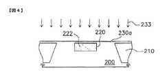
図4において、固相エピタキシー(Solid Phase Epitaxy)を行い、アモルファス系半導体層230を結晶性半導体層230aとするが、この結晶性半導体層230aは、半導体基板200と同じ材質なので、両者を一体化したものとして図示している。アモルファス系半導体層230をアモルファスシリコン層とする時、固相エピタキシー温度を500〜600℃の範囲とし、時間を1〜6時間とする。次に、チャネルイオン注入を行い、結晶性半導体層230a中へイオン233を注入するが、結晶性半導体層230aのトレンチ220の上方部分をチャネル領域とし、イオン233の注入ドーズ量を1×10¹²/cm2〜6×1013/cm2の範囲とする。もしもデバイスをNMOSとする場合、イオン233をP型イオン、例えば、ホウ素イオンとし、反対の場合には、N型イオン、例えば、リンイオンまたはヒ素イオンとする。
【0016】
この他に、上記のドーピングした結晶性半導体層230aを形成したい時、インサイチュウ(in situ)方式を採用することもでき、アモルファス系半導体層230を堆積する時、同時にドーピングを行ってから、固相エピタキシーを行い、ドーピングしたアモルファス系半導体層230を結晶性半導体層230aとすることができる。
【0017】
図5において、図5(b)は、図5(a)の切断線III − III' に沿って示した要部断面図である。次に、結晶性半導体層230aをパターニングして、素子領域230bを形成する。この素子領域230bは、犠牲層222の中間部分をまたいでおり、このようにして、半導体基板200と浅いトレンチ分離210と素子領域230bとにより2つのスリット226を取り囲むと同時に、犠牲層222のエッジ部分を露出させている。
【0018】
図6において、図6(b)は、図6(a)の切断線III − III' に沿って示した要部断面図であるが、図6(a)中には、符号240のゲート誘電層を図示していない。図6(a)において、等方性エッチングにより犠牲層222をエッチング除去し、素子領域230bをトレンチ220の上方を架空通過させるが、エッチング剤は、2つのスリット226を通って犠牲層222を完全に除去する。この等方性エッチングとしては、例えば、ウエットエッチングとし、犠牲層222の材質が窒化シリコンである時には、そのエッチング剤を熱リン酸(phosphoric acid)とする。図6(b)において、トレンチ220および領域230bの露出された表面上にゲート誘電層240、例えば、ゲート酸化層または窒化ゲート酸化層を形成するが、ゲート酸化層を形成する方法としては、熱酸化法(Thermal Oxidation)とし、窒化ゲート酸化層は、ゲート酸化層を形成した後で更に窒化することにより得られる。
【0019】
図7において、半導体基板200上に導体層250を形成するとともに、トレンチ220を充填するが、この導体層250の材質としては、例えば、ポリシリコン、ポリシリコン−ゲルマニウム、シリサイドまたは金属とし、その形成方法は、例えば、低圧化学気相堆積法(LPCVD)とする。
【0020】
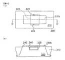
図8において、図8(b)は、図8(a)の切断線III − III' に沿って示した要部断面図であり、図8(c)は、図8(a)の切断線IV − IV' に沿って示した要部断面図であるが、図8(a)には、ゲート誘電層240を図示していない。図8に示すように、導体層250をパターニングしてゲート250aを形成するが、その位置は、トレンチ220中とトレンチ220の上方とであり、ゲート誘電層240を挟んで水平にトレンチ220上方の素子領域230bを包囲しており、この部分の素子領域230bをチャネル領域としている。
【0021】
図9において、ゲート250aをマスクとしてイオン注入260を行い、ゲート250aの両側の半導体基板200中にソース領域261およびドレイン領域262を形成する。しかし、ソース領域261およびドレイン領域262を形成する方法は、イオン注入法に限定されるものではなく、その他のドーピング方法、例えば、拡散式ドーピング法でも良い。
【0022】
さらには、図10において、同時に図7と図8(b)とを比較すると分かりやすいように、素子領域230bの下表面のゲート誘電層240上に導体層250ならびにゲート250aを形成する、つまり素子領域230bの下層を反転(Inversion)させるだけで良いのであるから、導体層250がトレンチ220を充填せずに、トレンチ220中に空洞273を形成しても良く、このようにして、ゲート250aのトレンチ220中の部分を中空ブロック状とし、図7と図8(b)と図9とに示した、むくブロック状(中実ブロック状)としないこともできる。
【0023】
また、図3〜図5において、ソース/ドレインもまたアモルファス半導体層230を形成する前に、イオン注入法により形成することができ、この時、犠牲層222によりソース領域とドレイン領域とを分離することができる。
【0024】
以上のごとく、この発明を好適な実施例により開示したが、もとより、この発明を限定するためのものではなく、当業者であれば容易に理解できるように、この発明の技術思想の範囲内において、適当な変更ならびに修正が当然なされうるものであるから、その特許権保護の範囲は、特許請求の範囲および、それと均等な領域を基準として定めなければならない。
【0025】
【発明の効果】
上記構成により、この発明にかかる金属酸化膜半導体電界効果型トランジスターとその製造方法は、デバイスのリーク電流を減少させ、起動電流を増大させることができるが、その理由は、次の通りである。
(1)この発明は、たいへん薄いドープド半導体層を形成してチャネル領域とすることができるので、チャネル領域がゲートから離れた領域ではなくなり、ゲートから離れた場所のリーク電流を徹底的に解消できる。
(2)この発明にかかる金属酸化膜半導体電界効果型トランジスター中のゲートは、トレンチ上方のチャネル領域を水平に包囲するので、チャネル領域の上下層がいずれもゲート電場の影響を受けることができ、デバイスの起動電流を増大させ、リーク電流を減少させることができる。また、この発明にかかる金属酸化膜半導体電界効果型トランジスターとその製造方法は、従来技術のFin FETデバイスの問題を解決することができるが、その理由は、次の通りである。第1に、この発明は、たいへん薄いドープド半導体層、例えば、エピタキシーシリコン層を使用してチャネル領域とすることができるので、SOI基板に取って代わることができ、高価なSOI基板を使用する必要がなくなり、製造コストを低減することができる。第2に、従来技術のFin FETデバイスのフィン状シリコン層120(図1を参照)と異なることは、この発明のドープド結晶性半導体層の表面、すなわち、そのチャネル領域の表面がドライエッチングによる破壊を受けないので、デバイスの性能に影響を与えないものとなる。
(3)この発明のソースおよびドレインは、一般的なドーピング方式により形成することができるので、従来技術のFin FETデバイスが隆起式ソース/ドレイン技術を採用しなければならないのと較べて、この発明の方が工程条件の制御において容易なものとなる。
(4)この発明にかかる金属酸化膜半導体電界効果型トランジスターは、水平構造のデバイス(チャネル領域表面と基板表面とが平行)であるので、後続の平坦化工程を容易に行うことができる。
(5)この発明は、ドープド結晶性半導体層の形成厚さによりチャネル領域の厚さを決定できるので、Fin FETデバイスのフィン状シリコン層を形成するために必要な電子ビームリソグラフィー技術がいらなくなり、しかも異方性エッチング工程の制御が難しいという問題もなくなる。
【0026】
従って、産業上の利用価値が高い。
【図面の簡単な説明】
【図1】(a)は、従来技術にかかるFin FETデバイスの構造を示す平面図、(b)(c)は、その要部断面図である。
【図2】(a)は、本発明の製造フローを示す平面図、(b)は、その要部断面図である。
【図3】本発明の製造フローを示す要部断面図である。
【図4】同じく、本発明の製造フローを示す要部断面図である。
【図5】(a)は、本発明の製造フローを示す平面図、(b)は、その要部断面図である。
【図6】(a)は、本発明の製造フローを示す平面図、(b)は、その要部断面図である。
【図7】本発明の製造フローを示す要部断面図である。
【図8】(a)は、本発明の製造フローを示す平面図、(b)(c)は、その要部断面図である。
【図9】本発明の製造フローを示す要部断面図である。
【図10】本発明の別な製造フローを示す要部断面図である。
【符号の説明】
200 半導体基板
210 浅いトレンチ分離
220 トレンチ
222 犠牲層
226 スリット
230 アモルファス半導体層
230a 結晶性半導体層
230b 素子領域
233 チャネルイオン注入
240 ゲート酸化層
250 導体層
250a ゲート
260 イオン注入
261 ソース領域
262 ドレイン領域
273 空洞[0001]
BACKGROUND OF THE INVENTION
The present invention relates to a structure of a semiconductor device and a manufacturing method thereof, and more particularly, to a metal oxide semiconductor field effect transistor (MOSFET) and a manufacturing method thereof.
[0002]
[Prior art]
As the line width of the metal oxide semiconductor (MOS) manufacturing process shrinks day by day, the leakage current (Leakage Current) becomes far from the gate between the source and drain. ) Is also increasing. Although this leakage current is reduced by the relatively thin gate dielectric layer, when the process line width is reduced to 0.1 μm or less, even if the gate dielectric layer is very thin, the leakage current Could not be reduced. In response to this problem, Professor Masaaki Hu (translation of the University of Berkeley, California) showed that there are two solutions. First, the MOSFET is formed by a very thin semiconductor substrate. Once manufactured, there is no place in the substrate away from the gate, and the leakage current at that place can be eliminated thoroughly. The second is to form a double gate structure. By surrounding the channel region with a dielectric layer in between, the entire channel region is affected by the gate electric field, increasing the device start-up current (On-current) and reducing the leakage current. .
[0003]
Accordingly, a fin field effect transistor (Fin FET, FinFET) that combines the two concepts described above has been disclosed, and its structure is shown in FIGS. 1 (a), (b), and (c). b) and (c) are cross-sectional views taken along section lines I-I 'and II-II' in FIG. The step of forming the fin field effect transistor is as follows. First, a silicon on insulating layer (SOI)
[0004]
Subsequently, in FIGS. 1A, 1B, and 1C, a conformal silicon nitride layer (not shown; before processing of reference numeral 160) is deposited on the
[0005]
[Problems to be solved by the invention]
In such a FinFET manufacturing method, since the fin-
[0006]
Accordingly, a first object of the present invention is to provide a structure of a metal oxide semiconductor field effect transistor capable of solving the above-described problems of Fin FETs with a small leakage current and a large starting current. The second object of the present invention is to reduce the leakage current of the device and increase the startup current of the device, and at the same time, solve the problems caused by the above-described FinFET device and its manufacturing method. An object of the present invention is to provide a method for manufacturing an effect transistor.
[0007]
[Means for Solving the Problems]
In order to solve the above problems and achieve a desired object, a metal oxide semiconductor field effect transistor according to the present invention includes a semiconductor substrate, a doped semiconductor layer, a gate dielectric layer, a gate, a source, and a drain. It consists of. Then, it is assumed that the semiconductor substrate has a trench, the doped semiconductor layer straddles the trench, and the outline does not completely enclosethe trench, that is, the trench is partially covered . The gate dielectric layer is located on the surface of the trench and the doped semiconductor layer, and the gate is located in and above the trench and surrounds the doped semiconductor layer with the gate dielectric layer interposed therebetween, but is surrounded by the gate. A part of the doped semiconductor layer becomes a channel region. When this gate horizontally surrounds the doped semiconductor layer, that is, when the gate dielectric layer between them is parallel to the surface of the semiconductor substrate, this gate is called a horizontal surrounding gate (Horizontal Surround Gate = HSG). The source and drain are located on both sides of the gate.
[0008]
Similarly, in order to solve the above-described problems and achieve a desired object, a metal oxide semiconductor field effect transistor manufacturing method according to the present invention includes a step of providing a semiconductor substrate, and a trench is formed on the semiconductor substrate. A step of filling the trench with a sacrificial layer, a step of covering the semiconductor substrate and the sacrificial layer with a doped semiconductor layer, and patterning the doped semiconductor layer to form an element region, the element region comprising: Straddling the sacrificial layer and exposing a portion of the sacrificial layer; removing the sacrificial layer; forming a gate dielectric layer on the surface of the trench and device region; and forming a conductor layer on the gate dielectric layer And filling the trench and patterning the conductor layer so that it is in and above the trench. And location, and consists of forming a gate surrounding the element region through the gate dielectric layer, and forming source and drain on either side of the gate.
[0009]
In the metal oxide semiconductor field effect transistor manufacturing method according to the present invention, the source and drain can be formed by ion implantation before forming the doped semiconductor layer. At this time, the sacrificial layer is used as the source. Can be used to isolate the drain.
[0010]
The metal oxide semiconductor field effect transistor and the manufacturing method thereof according to the present invention can reduce the leakage current of the device and increase the starting current. The reason for this will be described as follows. First, the present invention can form a very thin doped semiconductor layer to be a channel region, so that there can be no region far from the gate in the channel region, and thorough leakage current generated at a location far from the gate Can be resolved. Second, in the metal oxide semiconductor field effect transistor according to the present invention, since the gate surrounds the channel region above the trench, the upper and lower layers of the channel region can be affected by the gate electric field, The startup current of the device can be increased and the leakage current can be reduced.
[0011]
Furthermore, the metal oxide semiconductor field effect transistor and the manufacturing method thereof according to the present invention can also solve the problems of the above-described Fin FET device for the following reason. First, in the present invention, a very thin doped semiconductor layer can be formed to be a channel region, so that the SOI thin film can be replaced and there is no need to use an expensive SOI substrate. Second, since the surface of the doped semiconductor layer of the present invention, that is, the surface of the channel region is not damaged by dry etching, the function of the device is not affected. Third, since the source and drain of the present invention can be formed by general doping, the process conditions can be easily controlled. Fourth, since the metal oxide semiconductor field effect transistor according to the present invention is a device having a horizontal structure (the surface of the channel region and the surface of the substrate are parallel), the subsequent planarization process can be easily performed. . (5) The present invention allows the thickness of the channel region to be adjusted by the formation thickness of the doped semiconductor layer, so that it is not necessary to use the electron beam lithography technique necessary for manufacturing the FinFET device, and is anisotropic. There is no problem that control of etching is difficult.
[0012]
DETAILED DESCRIPTION OF THE INVENTION
DESCRIPTION OF EXEMPLARY EMBODIMENTS Hereinafter, preferred embodiments of the invention will be described with reference to the drawings.
[0013]
2A is a plan view showing a manufacturing flow of the metal oxide semiconductor field effect transistor according to the present invention, and FIG. 2B is a sectional view taken along the line III − in FIG. 2A. It is principal part sectional drawing shown along III '. First, a
[0014]
In FIG. 3, the
[0015]
In FIG. 4, solid phase epitaxy is performed, and the
[0016]
In addition, when it is desired to form the doped
[0017]
In FIG. 5, FIG. 5B is a cross-sectional view of the principal part taken along the cutting line III-III ′ in FIG. Next, the
[0018]
In FIG. 6, FIG. 6B is a cross-sectional view of the principal part taken along the section line III-III ′ in FIG. 6A. In FIG. Layers are not shown. In FIG. 6A, the
[0019]
In FIG. 7, the
[0020]
In FIG. 8, FIG. 8 (b) is a cross-sectional view of the principal part taken along the cutting line III-III ′ of FIG. 8 (a), and FIG. 8 (c) is the cutting line of FIG. FIG. 8 (a) does not show the
[0021]
In FIG. 9,
[0022]
Further, in FIG. 10, as easily understood by comparing FIG. 7 and FIG. 8B at the same time, the
[0023]
3 to 5, the source / drain can also be formed by ion implantation before the
[0024]
As described above, the present invention has been disclosed in the preferred embodiments. However, the present invention is not intended to limit the present invention and is within the scope of the technical idea of the present invention so that those skilled in the art can easily understand. Since appropriate changes and modifications can be naturally made, the scope of protection of the patent right must be determined on the basis of the scope of claims and an area equivalent thereto.
[0025]
【The invention's effect】
With the above configuration, the metal oxide semiconductor field effect transistor and the manufacturing method thereof according to the present invention can reduce the leakage current of the device and increase the starting current for the following reason.
(1) According to the present invention, since a very thin doped semiconductor layer can be formed as a channel region, the channel region is not a region away from the gate, and the leakage current away from the gate can be thoroughly eliminated. .
(2) Since the gate in the metal oxide semiconductor field effect transistor according to the present invention horizontally surrounds the channel region above the trench, both the upper and lower layers of the channel region can be affected by the gate electric field, The startup current of the device can be increased and the leakage current can be reduced. In addition, the metal oxide semiconductor field effect transistor and the manufacturing method thereof according to the present invention can solve the problems of the conventional FinFET device for the following reason. First, the present invention can use a very thin doped semiconductor layer, e.g., an epitaxial silicon layer, to form the channel region, which can replace the SOI substrate and requires the use of an expensive SOI substrate. The manufacturing cost can be reduced. Second, the surface of the doped crystalline semiconductor layer of the present invention, that is, the surface of its channel region is destroyed by dry etching, which is different from the fin-like silicon layer 120 (see FIG. 1) of the FinFET device of the prior art. Will not affect the performance of the device.
(3) Since the source and drain of the present invention can be formed by a general doping method, the present invention is different from the conventional Fin FET device that must adopt the raised source / drain technology. This is easier in controlling the process conditions.
(4) Since the metal oxide semiconductor field effect transistor according to the present invention is a device having a horizontal structure (the channel region surface and the substrate surface are parallel), the subsequent planarization step can be easily performed.
(5) In the present invention, since the thickness of the channel region can be determined by the formation thickness of the doped crystalline semiconductor layer, the electron beam lithography technique necessary for forming the fin-like silicon layer of the FinFET device is eliminated. Moreover, the problem that the anisotropic etching process is difficult to control is eliminated.
[0026]
Therefore, the industrial utility value is high.
[Brief description of the drawings]
FIG. 1A is a plan view showing a structure of a FinFET device according to the prior art, and FIGS. 1B and 1C are cross-sectional views of main parts thereof.
FIG. 2A is a plan view showing a manufacturing flow of the present invention, and FIG.
FIG. 3 is a cross-sectional view of a main part showing a manufacturing flow of the present invention.
FIG. 4 is a cross-sectional view of an essential part showing a manufacturing flow of the present invention.
5A is a plan view showing a manufacturing flow of the present invention, and FIG. 5B is a cross-sectional view of an essential part thereof.
6A is a plan view showing a manufacturing flow of the present invention, and FIG. 6B is a cross-sectional view of the main part thereof.
FIG. 7 is a cross-sectional view of the main part showing the manufacturing flow of the present invention.
8A is a plan view showing a manufacturing flow of the present invention, and FIGS. 8B and 8C are cross-sectional views of the main part thereof.
FIG. 9 is a cross-sectional view of the main part showing the manufacturing flow of the present invention.
FIG. 10 is a cross-sectional view of a principal part showing another manufacturing flow of the present invention.
[Explanation of symbols]
200
Claims (19)
Translated fromJapanese前記半導体基板上にトレンチを形成するステップと、
前記トレンチを犠牲層により充填するステップと、
前記半導体基板および前記犠牲層上をドープド半導体層で被覆するステップと、
前記ドープド半導体層をパターニングして素子領域を形成するものであって、前記素子領域が、前記犠牲層をまたぐとともに、前記犠牲層の一部分を露出させるステップと、
前記犠牲層を除去するステップと、
前記トレンチおよび前記素子領域の表面にゲート誘電層を形成するステップと、
前記ゲート誘電層上に導体層を形成するとともに、前記トレンチを充填するステップと、
前記導体層をパターニングして、前記トレンチ中および前記トレンチの上方に位置し、かつ前記ゲート誘電層を挟んで前記素子領域を包囲するゲートを形成するステップと、
前記ゲートの両側にソースおよびドレインを形成するステップと、
を具備し、
前記ソースおよびドレインは、前記素子領域を包囲する前記ゲートの両側において前記半導体基板中に形成され、
前記ソースおよび前記ドレインが、前記ドープド半導体層を形成する前に形成され、前記犠牲層により隔てられている
ことを特徴とする金属酸化膜半導体電界効果型トランジスターの製造方法。Providing a semiconductor substrate;
Forming a trench on the semiconductor substrate;
Filling the trench with a sacrificial layer;
Coating the semiconductor substrate and the sacrificial layer with a doped semiconductor layer;
Patterning the doped semiconductor layer to form an element region, the element region straddling the sacrificial layer and exposing a portion of the sacrificial layer;
Removing the sacrificial layer;
Forming a gate dielectric layer on a surface of the trench and the device region;
Forming a conductor layer on the gate dielectric layer and filling the trench;
Patterning the conductor layer to form a gate located in and above the trench and surrounding the device region with the gate dielectric layer in between;
Forming a source and a drain on both sides of the gate;
Comprising
The source and drain are formed in the semiconductor substrate on both sides of the gate surrounding the device region;
The method of manufacturing a metal oxide semiconductor field effect transistor,wherein the source and the drain are formed before forming the doped semiconductor layer and separated by the sacrificial layer .
前記半導体基板上に犠牲材料を堆積するとともに、前記トレンチを充填する小ステップと、
前記トレンチ以外の前記犠牲材料を除去する小ステップと、
を具備するものであることを特徴とする請求項1記載の金属酸化膜半導体電界効果型トランジスターの製造方法。Filling the trench with the sacrificial layer;
Depositing a sacrificial material on the semiconductor substrate and filling the trench;
A small step of removing the sacrificial material other than the trench;
Method for producing a metal oxide semiconductor field effect transistor according to claim1, characterized in that having a.
インサイチュウ(in situ)方式、即ち、堆積すると同時にドーピングを行う方式により、前記半導体基板上にドープドアモルファス系半導体層を形成するステップと、
固相エピタキシーにより前記ドープドアモルファス系半導体層を前記ドープド結晶性半導体層とするステップとを
具備するものであることを特徴とする請求項5記載の金属酸化膜半導体電界効果型トランジスターの製造方法。A method of forming the doped crystalline semiconductor layer includes:
Forming a doped amorphous semiconductor layer on the semiconductor substrate by an in situ method, that is, a method of doping at the same time as deposition; and
6. The method of manufacturing a metal oxide semiconductor field effect transistor according to claim5 , further comprising the step of using the doped amorphous semiconductor layer as the doped crystalline semiconductor layer by solid phase epitaxy.
固相エピタキシーにより前記アモルファス系半導体層を前記結晶性半導体層とするステップと、
前記結晶性半導体層へドーピングするステップと、
を具備するものであることを特徴とする請求項5記載の金属酸化膜半導体電界効果型トランジスターの製造方法。Forming the doped crystalline semiconductor layer by forming an amorphous semiconductor layer on the semiconductor substrate and the sacrificial layer; and
Making the amorphous semiconductor layer the crystalline semiconductor layer by solid phase epitaxy;
Doping the crystalline semiconductor layer;
The method of manufacturing a metal oxide semiconductor field effect transistor according to claim5 , comprising:
Priority Applications (1)
| Application Number | Priority Date | Filing Date | Title |
|---|---|---|---|
| JP2002378306AJP3983167B2 (en) | 2002-12-26 | 2002-12-26 | Method for manufacturing metal oxide semiconductor field effect transistor |
Applications Claiming Priority (1)
| Application Number | Priority Date | Filing Date | Title |
|---|---|---|---|
| JP2002378306AJP3983167B2 (en) | 2002-12-26 | 2002-12-26 | Method for manufacturing metal oxide semiconductor field effect transistor |
Publications (2)
| Publication Number | Publication Date |
|---|---|
| JP2004214228A JP2004214228A (en) | 2004-07-29 |
| JP3983167B2true JP3983167B2 (en) | 2007-09-26 |
Family
ID=32815217
Family Applications (1)
| Application Number | Title | Priority Date | Filing Date |
|---|---|---|---|
| JP2002378306AExpired - Fee RelatedJP3983167B2 (en) | 2002-12-26 | 2002-12-26 | Method for manufacturing metal oxide semiconductor field effect transistor |
Country Status (1)
| Country | Link |
|---|---|
| JP (1) | JP3983167B2 (en) |
Families Citing this family (5)
| Publication number | Priority date | Publication date | Assignee | Title |
|---|---|---|---|---|
| US7915659B2 (en)* | 2008-03-06 | 2011-03-29 | Micron Technology, Inc. | Devices with cavity-defined gates and methods of making the same |
| JP6570817B2 (en) | 2013-09-23 | 2019-09-04 | 株式会社半導体エネルギー研究所 | Semiconductor device |
| US10211088B2 (en) | 2015-09-10 | 2019-02-19 | Intel Corporation | Self-aligned isotropic etch of pre-formed vias and plugs for back end of line (BEOL) interconnects |
| US10490732B2 (en) | 2016-03-11 | 2019-11-26 | Toshiba Memory Corporation | Magnetic memory device with sidewall layer containing boron and manufacturing method thereof |
| TWI688001B (en) | 2016-09-14 | 2020-03-11 | 東芝記憶體股份有限公司 | Semiconductor device and its manufacturing method |
- 2002
- 2002-12-26JPJP2002378306Apatent/JP3983167B2/ennot_activeExpired - Fee Related
Also Published As
| Publication number | Publication date |
|---|---|
| JP2004214228A (en) | 2004-07-29 |
Similar Documents
| Publication | Publication Date | Title |
|---|---|---|
| KR100576361B1 (en) | 3D CMOS field effect transistor and method of manufacturing the same | |
| JP3998893B2 (en) | Method for forming T-type element isolation film | |
| JP4644173B2 (en) | Method for manufacturing transistor | |
| JP5286701B2 (en) | Semiconductor device and manufacturing method of semiconductor device | |
| KR101457007B1 (en) | Semiconductor device and semiconductor device manufacturing method | |
| KR100282452B1 (en) | Semiconductor device and method for fabricating the same | |
| KR101201489B1 (en) | Method for fabricating soi device | |
| KR100702553B1 (en) | NiFFT device formed from bulk semiconductor and method of manufacturing same | |
| JP2007250665A (en) | Semiconductor device and manufacturing method thereof | |
| CN101369598A (en) | semiconductor structure | |
| CN102891087A (en) | Semiconductor device structure insulated from a bulk silicon substrate and method of forming the same | |
| EP1147552A1 (en) | Field effect transistor structure with abrupt source/drain junctions | |
| US6649979B2 (en) | Method of manufacturing MOSFET and structure thereof | |
| TWI296851B (en) | Process for fabricating a strained channel mosfet device | |
| US6661044B2 (en) | Method of manufacturing MOSEFT and structure thereof | |
| US20090085075A1 (en) | Method of fabricating mos transistor and mos transistor fabricated thereby | |
| JP3983167B2 (en) | Method for manufacturing metal oxide semiconductor field effect transistor | |
| JP5525127B2 (en) | Semiconductor device and manufacturing method thereof | |
| US20050260818A1 (en) | Semiconductor device and method for fabricating the same | |
| TWI722515B (en) | Semiconductor device and method of manufacturing the same | |
| JP3986742B2 (en) | Memory cell forming method | |
| KR20070068736A (en) | A semiconductor device manufacturing method comprising a MOS transistor having multiple channels formed on an investment insulating film | |
| CN109273407B (en) | Semiconductor device and method of forming the same | |
| JP7741354B2 (en) | 3D transistor structures with precise geometries | |
| KR100400782B1 (en) | Method for fabricating of semiconductor device |
Legal Events
| Date | Code | Title | Description |
|---|---|---|---|
| A977 | Report on retrieval | Free format text:JAPANESE INTERMEDIATE CODE: A971007 Effective date:20060403 | |
| A131 | Notification of reasons for refusal | Free format text:JAPANESE INTERMEDIATE CODE: A131 Effective date:20060523 | |
| A521 | Request for written amendment filed | Free format text:JAPANESE INTERMEDIATE CODE: A523 Effective date:20060821 | |
| A131 | Notification of reasons for refusal | Free format text:JAPANESE INTERMEDIATE CODE: A131 Effective date:20061212 | |
| A521 | Request for written amendment filed | Free format text:JAPANESE INTERMEDIATE CODE: A523 Effective date:20070305 | |
| TRDD | Decision of grant or rejection written | ||
| A01 | Written decision to grant a patent or to grant a registration (utility model) | Free format text:JAPANESE INTERMEDIATE CODE: A01 Effective date:20070605 | |
| A61 | First payment of annual fees (during grant procedure) | Free format text:JAPANESE INTERMEDIATE CODE: A61 Effective date:20070703 | |
| FPAY | Renewal fee payment (event date is renewal date of database) | Free format text:PAYMENT UNTIL: 20100713 Year of fee payment:3 | |
| R150 | Certificate of patent or registration of utility model | Free format text:JAPANESE INTERMEDIATE CODE: R150 Ref document number:3983167 Country of ref document:JP Free format text:JAPANESE INTERMEDIATE CODE: R150 | |
| FPAY | Renewal fee payment (event date is renewal date of database) | Free format text:PAYMENT UNTIL: 20100713 Year of fee payment:3 | |
| FPAY | Renewal fee payment (event date is renewal date of database) | Free format text:PAYMENT UNTIL: 20110713 Year of fee payment:4 | |
| R250 | Receipt of annual fees | Free format text:JAPANESE INTERMEDIATE CODE: R250 | |
| FPAY | Renewal fee payment (event date is renewal date of database) | Free format text:PAYMENT UNTIL: 20110713 Year of fee payment:4 | |
| FPAY | Renewal fee payment (event date is renewal date of database) | Free format text:PAYMENT UNTIL: 20120713 Year of fee payment:5 | |
| R250 | Receipt of annual fees | Free format text:JAPANESE INTERMEDIATE CODE: R250 | |
| FPAY | Renewal fee payment (event date is renewal date of database) | Free format text:PAYMENT UNTIL: 20120713 Year of fee payment:5 | |
| FPAY | Renewal fee payment (event date is renewal date of database) | Free format text:PAYMENT UNTIL: 20130713 Year of fee payment:6 | |
| R250 | Receipt of annual fees | Free format text:JAPANESE INTERMEDIATE CODE: R250 | |
| R250 | Receipt of annual fees | Free format text:JAPANESE INTERMEDIATE CODE: R250 | |
| R250 | Receipt of annual fees | Free format text:JAPANESE INTERMEDIATE CODE: R250 | |
| R250 | Receipt of annual fees | Free format text:JAPANESE INTERMEDIATE CODE: R250 | |
| R250 | Receipt of annual fees | Free format text:JAPANESE INTERMEDIATE CODE: R250 | |
| R250 | Receipt of annual fees | Free format text:JAPANESE INTERMEDIATE CODE: R250 | |
| R250 | Receipt of annual fees | Free format text:JAPANESE INTERMEDIATE CODE: R250 | |
| R250 | Receipt of annual fees | Free format text:JAPANESE INTERMEDIATE CODE: R250 | |
| R250 | Receipt of annual fees | Free format text:JAPANESE INTERMEDIATE CODE: R250 | |
| R250 | Receipt of annual fees | Free format text:JAPANESE INTERMEDIATE CODE: R250 | |
| LAPS | Cancellation because of no payment of annual fees |