JP3981898B2 - Signal receiving apparatus and method, and recording medium - Google Patents
Signal receiving apparatus and method, and recording mediumDownload PDFInfo
- Publication number
- JP3981898B2 JP3981898B2JP03830998AJP3830998AJP3981898B2JP 3981898 B2JP3981898 B2JP 3981898B2JP 03830998 AJP03830998 AJP 03830998AJP 3830998 AJP3830998 AJP 3830998AJP 3981898 B2JP3981898 B2JP 3981898B2
- Authority
- JP
- Japan
- Prior art keywords
- signal
- ofdm
- guard interval
- circuit
- interpolation
- Prior art date
- Legal status (The legal status is an assumption and is not a legal conclusion. Google has not performed a legal analysis and makes no representation as to the accuracy of the status listed.)
- Expired - Fee Related
Links
- 238000000034methodMethods0.000titleclaimsdescription38
- 230000005540biological transmissionEffects0.000claimsdescription44
- 238000001514detection methodMethods0.000claimsdescription42
- 238000012545processingMethods0.000claimsdescription23
- 238000000605extractionMethods0.000claimsdescription11
- 238000004364calculation methodMethods0.000description23
- 238000010586diagramMethods0.000description10
- 230000010354integrationEffects0.000description6
- 238000012937correctionMethods0.000description5
- 239000000284extractSubstances0.000description5
- 230000003111delayed effectEffects0.000description2
- 230000000694effectsEffects0.000description2
- 238000005070samplingMethods0.000description2
- 239000000969carrierSubstances0.000description1
- 238000004891communicationMethods0.000description1
- 238000004590computer programMethods0.000description1
- 238000005562fadingMethods0.000description1
- 238000003780insertionMethods0.000description1
- 230000037431insertionEffects0.000description1
- 238000012544monitoring processMethods0.000description1
- 230000010363phase shiftEffects0.000description1
- 230000008054signal transmissionEffects0.000description1
- 239000007787solidSubstances0.000description1
- 230000005236sound signalEffects0.000description1
- 238000012546transferMethods0.000description1
Images


Classifications
- H—ELECTRICITY
- H04—ELECTRIC COMMUNICATION TECHNIQUE
- H04L—TRANSMISSION OF DIGITAL INFORMATION, e.g. TELEGRAPHIC COMMUNICATION
- H04L27/00—Modulated-carrier systems
- H04L27/26—Systems using multi-frequency codes
- H04L27/2601—Multicarrier modulation systems
- H04L27/2647—Arrangements specific to the receiver only
- H04L27/2655—Synchronisation arrangements
- H04L27/2666—Acquisition of further OFDM parameters, e.g. bandwidth, subcarrier spacing, or guard interval length
- H—ELECTRICITY
- H04—ELECTRIC COMMUNICATION TECHNIQUE
- H04L—TRANSMISSION OF DIGITAL INFORMATION, e.g. TELEGRAPHIC COMMUNICATION
- H04L5/00—Arrangements affording multiple use of the transmission path
- H04L5/003—Arrangements for allocating sub-channels of the transmission path
- H04L5/0048—Allocation of pilot signals, i.e. of signals known to the receiver
- H—ELECTRICITY
- H04—ELECTRIC COMMUNICATION TECHNIQUE
- H04L—TRANSMISSION OF DIGITAL INFORMATION, e.g. TELEGRAPHIC COMMUNICATION
- H04L25/00—Baseband systems
- H04L25/02—Details ; arrangements for supplying electrical power along data transmission lines
- H04L25/0202—Channel estimation
- H04L25/022—Channel estimation of frequency response
- H—ELECTRICITY
- H04—ELECTRIC COMMUNICATION TECHNIQUE
- H04L—TRANSMISSION OF DIGITAL INFORMATION, e.g. TELEGRAPHIC COMMUNICATION
- H04L25/00—Baseband systems
- H04L25/02—Details ; arrangements for supplying electrical power along data transmission lines
- H04L25/0202—Channel estimation
- H04L25/0224—Channel estimation using sounding signals
- H04L25/0228—Channel estimation using sounding signals with direct estimation from sounding signals
- H04L25/023—Channel estimation using sounding signals with direct estimation from sounding signals with extension to other symbols
- H04L25/0232—Channel estimation using sounding signals with direct estimation from sounding signals with extension to other symbols by interpolation between sounding signals
- H—ELECTRICITY
- H04—ELECTRIC COMMUNICATION TECHNIQUE
- H04L—TRANSMISSION OF DIGITAL INFORMATION, e.g. TELEGRAPHIC COMMUNICATION
- H04L25/00—Baseband systems
- H04L25/02—Details ; arrangements for supplying electrical power along data transmission lines
- H04L25/03—Shaping networks in transmitter or receiver, e.g. adaptive shaping networks
- H04L25/03006—Arrangements for removing intersymbol interference
- H04L25/03159—Arrangements for removing intersymbol interference operating in the frequency domain
- H—ELECTRICITY
- H04—ELECTRIC COMMUNICATION TECHNIQUE
- H04L—TRANSMISSION OF DIGITAL INFORMATION, e.g. TELEGRAPHIC COMMUNICATION
- H04L27/00—Modulated-carrier systems
- H04L27/01—Equalisers
- H—ELECTRICITY
- H04—ELECTRIC COMMUNICATION TECHNIQUE
- H04L—TRANSMISSION OF DIGITAL INFORMATION, e.g. TELEGRAPHIC COMMUNICATION
- H04L27/00—Modulated-carrier systems
- H04L27/26—Systems using multi-frequency codes
- H04L27/2601—Multicarrier modulation systems
- H04L27/2647—Arrangements specific to the receiver only
- H04L27/2655—Synchronisation arrangements
- H04L27/2668—Details of algorithms
- H04L27/2673—Details of algorithms characterised by synchronisation parameters
- H04L27/2675—Pilot or known symbols
- H—ELECTRICITY
- H04—ELECTRIC COMMUNICATION TECHNIQUE
- H04L—TRANSMISSION OF DIGITAL INFORMATION, e.g. TELEGRAPHIC COMMUNICATION
- H04L25/00—Baseband systems
- H04L25/02—Details ; arrangements for supplying electrical power along data transmission lines
- H04L25/03—Shaping networks in transmitter or receiver, e.g. adaptive shaping networks
- H04L25/03006—Arrangements for removing intersymbol interference
- H04L2025/0335—Arrangements for removing intersymbol interference characterised by the type of transmission
- H04L2025/03375—Passband transmission
- H04L2025/03414—Multicarrier
- H—ELECTRICITY
- H04—ELECTRIC COMMUNICATION TECHNIQUE
- H04L—TRANSMISSION OF DIGITAL INFORMATION, e.g. TELEGRAPHIC COMMUNICATION
- H04L25/00—Baseband systems
- H04L25/02—Details ; arrangements for supplying electrical power along data transmission lines
- H04L25/03—Shaping networks in transmitter or receiver, e.g. adaptive shaping networks
- H04L25/03006—Arrangements for removing intersymbol interference
- H04L2025/03433—Arrangements for removing intersymbol interference characterised by equaliser structure
- H04L2025/03439—Fixed structures
- H04L2025/03522—Frequency domain
- H—ELECTRICITY
- H04—ELECTRIC COMMUNICATION TECHNIQUE
- H04L—TRANSMISSION OF DIGITAL INFORMATION, e.g. TELEGRAPHIC COMMUNICATION
- H04L5/00—Arrangements affording multiple use of the transmission path
- H04L5/0001—Arrangements for dividing the transmission path
- H04L5/0003—Two-dimensional division
- H04L5/0005—Time-frequency
- H04L5/0007—Time-frequency the frequencies being orthogonal, e.g. OFDM(A) or DMT
Landscapes
- Engineering & Computer Science (AREA)
- Signal Processing (AREA)
- Computer Networks & Wireless Communication (AREA)
- Power Engineering (AREA)
- Noise Elimination (AREA)
- Digital Transmission Methods That Use Modulated Carrier Waves (AREA)
- Cable Transmission Systems, Equalization Of Radio And Reduction Of Echo (AREA)
Description
Translated fromJapanese【0001】
【発明の属する技術分野】
本発明は、信号受信装置および方法、並びに記録媒体に関し、特に、受信したOFDM信号のガードインタバルの長さに対応して補間フィルタの特性を切り替えることにより、伝送路における雑音の影響をより効果的に抑制することができるようにした、信号受信装置および方法、並びに記録媒体に関する。
【0002】
【従来の技術】
地上波を用いたデジタル放送の伝送方式として、最近、OFDM(Orthogonal Frequency Division Multiplex)変調方式(直交周波数分割多重方式)が注目されている。このOFDM変調方式を用いたサービスとして、欧州においては、Eureka 147 DAB(Digital Audio Broadcasting)方式を用いたラジオサービスが既に開始されている。また、テレビジョン放送に関しても、欧州において、既にDVB(Digital Video Broadcasting)-T方式が開発されており、ITU-R(International Telecommunication Union-Recommendation)においても、標準化が勧告されている。
【0003】
既にサービスが開始されているEureka 147 DAB方式では、主たるサービスとして、移動体音声信号を前提にしているため、OFDMの各搬送波は、π/4オフセット差動QPSK(Quadrature Phase Shift Keying)が用いられている。これは、この方式が移動体を前提にしているところから、フェーディングに対して耐性を持つことが必要条件になるため、振幅方向に情報を持たず、また、絶対位相を再生する必要もないことなどが、その採用の理由と考えられる。
【0004】
一方、テレビジョン放送においては、音声を対象とした放送サービスとは異なり、移動体への対応はそれほど大きな必要性がない代わりに、情報量の大きなビデオ情報を主に送信する必要があることから、高い伝送速度が求められる。すなわち、移動体音声サービスにおいては、劣悪な環境下でも、信頼性の高い伝送が要求されるのに対し、テレビジョン放送サービスにおいては、高速伝送が要求される。このような背景から、テレビジョン放送サービスを前提にしたDVB-T方式においては、OFDMの各搬送波の変調に、QPSK,64QAM,16QAMなどの変調方式を用いることが提案されている。
【0005】
また、地上波伝送においては、一般的に、マルチパスが存在し、このマルチパスにより、受信信号の周波数特性が歪むことになるので、このマルチパスの影響を軽減することが大きな課題となる。そこで、OFDM方式では、本来伝送すべき信号の一部をコピーした信号をガードインタバルとして付加するようにしている。このガードインタバルを付加することにより、ガードインタバルよりも短いマルチパスに関しては、受信側で適切な信号処理を施すことで、マルチパスの影響を除去することが可能となる。
【0006】
各搬送波の変調方式にQAM系の変調を用いるDVB-T方式のようなOFDM変調方式においては、マルチパスによる歪みが発生すると、各搬送波毎に、その振幅や位相が、送信側の振幅や位相と異なるものとなるので、これらが等しくなるように、マルチパスによる歪みを受けた信号を等化する(補正する)必要がある。OFDM方式では、受信側でFFT(Fast Fourier Transform)(高速フーリエ変換)を行って、OFDM復調を行うため、伝送信号中にパイロット信号を散在させておき、このパイロット信号の振幅や位相を受信側において監視することで、伝送路の特性を推定し、この推定した伝送路の特性で受信信号を等化するようにしている。
【0007】
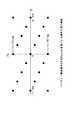
DVB-T方式においては、図9に示すようなパターンでパイロット信号を挿入することが提案されている。同図に示すように、この例においては、1つのOFDMシンボルの12本の搬送波に対して1本の割合で、パイロット用の搬送波信号が挿入され、さらにOFDMシンボル毎に、パイロット用の搬送波信号の挿入位置が、3搬送波ずつシフトされるようになされている。
【0008】
この図9に示した、時間方向と周波数方向に離散的に配列されたパイロット信号を2次元フーリエ変換して、その標本化格子点構造を調べ、伝送帯域幅を調べると、図10に示すようになる。同図より、伝送路に時間方向の変動がない場合の伝送帯域幅は、3本分の搬送波間隔に相当する時間以内であることが判る。換言すれば、OFDMシンボルの有効時間(ガードインタバルを除いたOFDMシンボルの継続時間)の1/3の伝送帯域幅があるので、DVB-T方式のパイロット信号パターンは、OFDM有効シンボル長の1/3以内の時間に対する等化能力があることになる。
【0009】
図11は、このようなパイロット信号から伝送路特性を推定し、受信信号を等化(補正)する、従来の信号受信装置の構成例を表している。チューナ2は、アンテナ1で受信した信号を中間周波信号(IF信号)に変換し、乗算器3と乗算器4に出力している。乗算器3と乗算器4には、搬送波生成回路7で生成された位相が相互に90度異なる搬送波が供給されている。乗算器3と乗算器4は、それぞれ、入力された中間周波信号と搬送波とを乗算し、ベースバンド(基底帯域)のOFDM信号に変換して、FFT回路5に出力している。FFT回路5は、入力された信号をFFT処理することで、ベースバンドのOFDM信号をOFDM復調する。
【0010】
FFTウインドウ回路6は、乗算器3と乗算器4の出力するベースバンドのOFDM信号から、OFDM信号のガードインタバルの相関を利用して、FFT回路5のFFT演算の開始の基準となるウインドウを生成し、FFT回路5に出力している。搬送波生成回路7は、FFTウインドウ回路6の出力から、位相が90度異なる搬送波を生成し乗算器3と乗算器4に出力している。
【0011】
FFT回路5が出力するOFDM信号の各搬送波は、等化回路13を構成する除算回路10とパイロット信号抽出回路8に供給される。パイロット信号抽出回路8は、入力された信号からパイロット信号を抽出し、補間フィルタ9に出力している。補間フィルタ9は、入力されたパイロット信号を補間処理することで、OFDM信号の各搬送波の伝送路特性を推定し、推定結果を除算回路10に出力している。除算回路10は、FFT回路5より入力されたOFDM信号の各搬送波を、補間フィルタ9より入力された伝送路特性で除算し、伝送路での歪みを除去し、デマッピング回路11に出力するようになされている。デマッピング回路11は、除算回路10より入力された信号の信号点より伝送情報を復元する。デマッピング回路11の後段に畳み込み符号などの誤り訂正回路が存在する場合には、このデマッピング回路11において、ビタビ復号器に供給するためのメトリックが生成される。
【0012】
TPS検出回路12は、FFT回路5の出力から、TPS(Transfer Parameter Signal)と称される伝送制御信号を抽出する。この伝送制御信号は、次のスーパーフレーム(8個のフレームにより1つのスーパーフレームが構成されている)における畳み込み符号の符号化率、OFDM搬送波の変調方式、ガードインタバル情報などを含んでいる。TPS検出回路12は、抽出した伝送制御信号に基づいて、各回路を制御する。例えば、伝送制御信号に含まれるOFDM搬送波の変調方式に基づいて、デマッピング回路11を制御し、QPSK,16QAM,64QAMなどの変調方式に対応したデマッピング処理を実行させる。
【0013】
次に、その動作について説明する。チューナ2は、アンテナ1で受信した信号を中間周波信号に変換し、乗算器3と乗算器4に出力する。乗算器3と乗算器4には、搬送波生成回路7で生成した、位相が90度異なる搬送波が供給されている。この搬送波は、乗算器3と乗算器4の出力から、FFTウインドウ回路6が、ガードインタバルの相関を利用して検出した位相誤差に対応して生成されたものである。乗算器3と乗算器4は、それぞれチューナ2より入力されたOFDM信号の中間周波信号と、搬送波生成回路7より供給された搬送波とを乗算し、ベースバンドのOFDM信号を生成し、FFT回路5に出力する。FFT回路5は、入力されたベースバンドのOFDM信号をFFT処理して、OFDM信号を復調する。
【0014】
パイロット信号抽出回路8は、FFT回路5の出力からパイロット信号を抽出し、補間フィルタ9に出力する。補間フィルタ9は、パイロット信号抽出回路8より入力されたパイロット信号を補間処理することで、各搬送波の振幅と位相成分を、その搬送波の伝送路特性として検出し、これを除算回路10に出力する。除算回路10は、FFT回路5より入力された復調信号を、補間フィルタ9から供給された振幅と位相で除算し、伝送路特性に起因する歪み成分を除去する。例えば、FFT回路5より入力される搬送波の振幅が、本来の振幅の1/2である場合、補間フィルタ9より振幅情報として、1/2が供給される。そこで、除算回路10で、FFT回路5より入力された信号の振幅を補間フィルタ9の振幅情報で除算すれば、元の1(=(1/2)/(1/2))の振幅の信号を得ることができる。同様に、位相についても、複素演算を行うことで、元の位相の信号を得ることができる。
【0015】
デマッピング回路11は、除算回路10より出力された信号の信号点をデマッピングする。TPS検出回路12は、このため、FFT回路5より出力される信号に含まれる伝送制御信号を検出し、その伝送制御信号からOFDM信号の変調方式に関する情報を検出し、その検出結果をデマッピング回路11に出力する。デマッピング回路11は、TPS検出回路12からの変調方式情報に対応してデマッピング処理を行い、処理結果を出力する。
【0016】
【発明が解決しようとする課題】
ところで、DVB-T方式においては、ガードインタバルの長さが、有効シンボル長の長さに対する割合として、1/4,1/8,1/16、または1/32の4種類が定義されている。補間フィルタ9は、4種類のうちのいずれの長さのガードインタバルの信号が受信されたとしても等化処理を行うことができるように、ガードインタバルが最大の長さの1/4の帯域幅に設定(固定)されている。
【0017】
このように、従来の装置は、補間フィルタ9の帯域幅が、ガードインタバルが最も長い1/4の場合に固定されているため、ガードインタバルが、それより短いOFDM信号を受信した場合には、そのとき、本来必要とされない信号成分の帯域を処理することとなり、結局、その信号に付随してノイズも多くなり、ノイズの影響により、より正確な伝送路推定処理が実現できなくなる課題があった。
【0018】
本発明はこのような状況に鑑みてなされたものであり、ノイズによる影響を軽減させることができるようにするものである。
【0019】
【課題を解決するための手段】
本発明の一側面の信号受信装置は、OFDM方式で伝送された信号を受信する信号受信装置であって、前記OFDM方式で伝送された信号を受信する受信手段と、前記受信手段で受信した前記OFDM信号を復調する復調手段と、前記受信手段で受信した前記OFDM信号のガードインタバルの長さを検出する検出手段と、前記OFDM信号を補間処理することにより前記OFDM信号の伝送特性を推定する補間手段と、前記検出手段により検出された前記ガードインタバルの長さに対応して、前記補間手段の帯域幅を制御する制御手段とを備えることを特徴とする。
前記復調手段で復調した信号を等化する等化手段をさらに設けるようにさせることができ、前記等化手段には、前記OFDM方式で伝送された信号に含まれるパイロット信号を抽出する抽出手段と、前記補間手段で推定した伝送特性で、前記復調手段で復調された信号を除算する除算手段とを含ませるようにすることができ、前記除算手段による除算結果を用いて、前記復調した信号を等化させるようにすることができ、前記補間手段には、前記抽出手段で抽出された前記パイロット信号を補間処理することにより、前記OFDM信号の伝送特性を推定させるようにすることができる。
前記補間手段は、補間フィルタとすることができ、前記制御手段には、前記補間フィルタの帯域幅を制御させるようにすることができる。
前記制御手段には、前記ガードインタバルの長さが短いとき、前記補間フィルタの帯域幅を短くするようにさせることができる。
前記検出手段には、前記ガードインタバルの相関を利用して、前記ガードインタバルの長さを検出させるようにすることができる。
前記検出手段には、前記OFDM信号に含めて伝送されてくるガードインタバル情報から、前記ガードインタバルの長さを検出させるようにすることができる。
【0020】
本発明の一側面の信号受信方法は、OFDM方式で伝送された信号を受信する信号受信装置の信号受信方法であって、前記OFDM方式で伝送された信号を受信する受信ステップと、前記受信ステップで受信した前記OFDM信号を復調する復調ステップと、前記受信ステップで受信した前記OFDM信号のガードインタバルの長さを検出する検出ステップと、前記OFDM信号を補間処理することにより前記OFDM信号の伝送特性を推定する補間ステップと、前記検出ステップでの処理により検出された前記ガードインタバルの長さに対応して、前記補間ステップの処理の帯域幅を制御する制御ステップとを含む。
【0021】
本発明の一側面の記録媒体のプログラムは、OFDM方式で伝送された信号を受信する信号受信装置に、前記OFDM方式で伝送された信号を受信する受信ステップと、前記受信ステップで受信した前記OFDM信号を復調する復調ステップと、前記受信ステップで受信した前記OFDM信号のガードインタバルの長さを検出する検出ステップと、前記OFDM信号を補間処理することにより前記OFDM信号の伝送特性を推定する補間ステップと、前記検出ステップの処理により検出された前記ガードインタバルの長さに対応して、前記補間ステップの処理の帯域幅を制御する制御ステップとを含む処理をコンピュータに実行させる。
【0022】
【発明の効果】
本発明の一側面の信号受信装置および方法、並びに記録媒体によれば、OFDM方式で伝送された信号が受信され、受信した前記OFDM信号が復調され、受信した前記OFDM信号のガードインタバルの長さが検出され、OFDM信号が補間処理されることによりOFDM信号の伝送特性が推定され、検出されたガードインタバルの長さに対応して、前記補間処理の帯域幅が制御される。
【0023】
【発明の実施の形態】
以下に本発明の実施の形態を説明するが、特許請求の範囲に記載の発明の各手段と以下の実施の形態との対応関係を明らかにするために、各手段の後の括弧内に、対応する実施の形態(但し一例)を付加して本発明の特徴を記述すると、次のようになる。但し勿論この記載は、各手段を記載したものに限定することを意味するものではない。
【0024】
請求項1に記載の信号受信装置は、OFDM方式で伝送された信号を受信する受信手段(例えば、図1のチューナ2)と、受信手段で受信したOFDM信号を復調する復調手段(例えば、図1のFFT回路5)と、復調手段で復調した信号を等化する等化手段(例えば、図1の等化回路13)と、受信手段で受信したOFDM信号のガードインタバルの長さを検出する検出手段(例えば、図1のFFTウインドウ回路6)と、検出手段の検出結果に対応して、等化手段を制御する制御手段(例えば、図1の制御回路21)とを備えることを特徴とする。
【0025】
請求項2に記載の信号受信装置は、等化手段が、OFDM方式で伝送された信号に含まれるパイロット信号を抽出する抽出出手段(例えば、図1のパイロット信号抽出回路8)と、抽出手段で抽出されたパイロット信号から、OFDM信号の伝送特性を補間する補間手段(例えば、図1の補間フィルタ9)と、補間手段で補間した伝送特性で、復調手段で復調された信号を除算する除算手段(例えば、図1の除算回路10)とを備えることを特徴とする。
【0026】
図1は、本発明を適用した信号受信装置の構成例を示すブロック図であり、図11に対応する部分には、同一の符号を付してあり、その説明は、適宜省略する。
【0027】
すなわち、図1の信号受信装置は、基本的に、図11に示した信号受信装置と同様の構成を有しており、FFTウインドウ回路6がガードインタバルの長さを検出し、その検出信号を制御回路21に出力するとともに、制御回路21が、FFTウインドウ回路6からの信号に対応して、補間フィルタ9を制御するようになされている点が、図11の例と異なっている。その他の構成は、図11における場合と同様である。
【0028】
図2は、図1のFFTウインドウ回路6の構成例を表している。乗算器3と乗算器4の出力は、それぞれ、有効時間遅延回路31と有効時間遅延回路32により、有効シンボル長に対応する時間τだけ遅延された後、複素相関計算回路33に入力されている。複素相関計算回路33にはまた、乗算器3と乗算器4より出力されたベースバンドのOFDM信号が、そのまま入力されている。複素相関計算回路33は、乗算器3より入力された信号をf(t)とし、有効時間遅延回路31より入力された信号をf(t−τ)とするとき、次式から、両者の相関iを演算する。
【0029】
【数1】
同様の処理が乗算器4の出力に対しても行われ、相関qが出力される。
【0031】
複素相関計算回路33の出力iとqは、絶対値回路34と位相検出回路37に供給されている。絶対値回路34は、入力された信号iとqの絶対値を、(i2+q2)1/2として演算する。絶対値回路34の出力は、ピーク検出回路35に供給される。ピーク検出回路35は、絶対値回路34より入力された絶対値と、予め設定されている所定の基準値とを比較し、基準値以上の絶対値が得られたとき、所定の相関が得られたと判定し、検出信号を判定回路36に出力している。
【0032】
判定回路36は、図3のフローチャートに示す処理を実行して、FFT回路5に内蔵するカウンタの出力を、FFT回路5がFFT演算を開始するタイミングの基準となる基準パルス(ウインドウ)として、FFT回路5に出力するとともに、ガードインタバル長を検出し、検出結果を制御回路21に出力する。判定回路36はまた、図3のフローチャートに示す処理を実行して、複素相関計算回路33に、相関計算における積分の期間Δを更新させるための信号を出力する。
【0033】
位相検出回路37は、複素相関計算回路33より入力された信号iとqの位相差をtan-1(q/i)として検出し、検出した位相誤差を搬送波生成回路7に出力している。
【0034】
次に、図3のフローチャートを参照して、FFTウインドウ回路6の動作を中心に、図1の実施の形態の、従来と異なる動作について説明する。最初にステップS1において、1つのOFDMシンボルの相関値のピークを検出する処理が実行される。すなわち、複素相関計算回路33には、乗算器3,4より、図4(A)に示すシンボルf(t)が入力されるとともに、有効時間遅延回路31,32を介して、図4(B)に示すシンボルf(t−τ)が入力される。シンボルf(t−τ)は、シンボルf(t)に対して、有効シンボル長に対応する時間τだけ遅延されており、図4に示すように、シンボルf(t)とシンボルf(t−τ)のガードインタバルが、同一のタイミングで複素相関計算回路33に入力されることになる。
【0035】
複素相関計算回路33は、上記式(1)に従って、シンボルf(t)とシンボルf(t−τ)の複素相関を演算する。
【0036】
この演算は、乗算器3の出力する信号と、有効時間遅延回路31の出力する信号との間で行われるとともに、乗算器4の出力する信号と、有効時間遅延回路32の出力する信号との間において行われる。前者の演算結果がiとして出力され、後者の演算結果がqとして出力される。
【0037】
絶対値回路34は、信号iを自乗した値と信号qを自乗した値の平方根を絶対値として演算し、ピーク検出回路35に出力する。
【0038】
複素相関計算回路33が、上記式(1)において、積分処理を行う期間Δが、図4に示すように、ガードインタバルの期間Δ0と等しい場合、絶対値回路34の出力する絶対値は、図5(A)に示すように、ガードインタバルの期間において大きな値を有するものとなる。これに対して、複素相関計算回路33が行う積分の期間Δが、ガードインタバルの期間Δ0と等しくない場合、絶対値回路34の出力は、図5(B)に示すように、それほど大きな値にはならない。しかしながら、いずれの場合においても、ガードインタバルの期間においては、ガードインタバルでない期間に較べて大きな値となる。ピーク検出回路35の基準値は、図5(A)に示す場合と、図5(B)に示す場合のいずれの場合をも検出するように、その基準値が予め設定されている。
【0039】
ピーク検出回路35より、基準値以上の絶対値が検出されたことを表す検出信号が入力されたとき、判定回路36は、ステップS2において、内蔵するタイマのそのときの現在時刻をtp1に設定する。
【0040】
次に、ステップS3において、上述したステップS1における場合と同様の処理が、次のOFDMシンボルについて実行される。そして、ステップS4において、上述したステップS2における場合と同様の処理が実行され、基準値以上の絶対値が検出された時刻が、tp2に設定される。
【0041】
判定回路36は、ステップS5において、ステップS4で求められた時刻tp2と、ステップS2で求められた時刻tp1の差(tp2−tp1)が、有効シンボル長τと、複素相関計算回路33で積分処理が行われた時間Δの和(τ+Δ)に近い値であるか否かを判定する。すなわち、次式が成立するか否かを判定する。
|(tp2−tp1)−(τ+Δn)|≦R1 (2)
【0042】
ここで、R1は、充分小さい基準値である。従って、上記(2)式が成立するということは、複素相関計算回路33における積分期間Δが、ガードインタバルの期間Δ0にほぼ等しいことを意味する。逆に、上記式(2)が満足されないということは、複素相関計算回路33における積分期間Δが、ガードインタバルの期間Δ0と等しくないことを意味する。この場合、ステップS6に進み、判定回路36は、複素相関計算回路33に積分期間Δを更新させる処理を実行する。すなわち、上述したように、ガードインタバルの期間としては、1/4,1/8,1/16,1/32の4種類が用意されているので、例えば、いまΔが1/4に対応する値に設定されている場合には、次に、Δを1/8に対応する値に更新させる。そして、ステップS1に戻り、同様の処理が繰り返し実行される。
【0043】
一方、ステップS5において、上記式(2)が満足されたと判定された場合、ステップS7に進み、判定回路36は、そのときのガードインタバルの長さに対応する値を制御回路21に出力する。制御回路21に入力される。制御回路21は、入力されたガードインタバルの長さに対応するように、補間フィルタ9の帯域幅を制御する。ガードインタバルの長さが長いとき、補間フィルタ9の帯域幅は長くされ、ガードインタバルの長さが短いとき、補間フィルタ9の帯域幅は短くされる。従って、補間フィルタ9の帯域幅は、ガードインタバルが1/4のとき最も長くなり、1/32のとき最も短くなるように制御される。これにより、補間フィルタ9は、必要最小限の範囲のパイロット信号だけを処理することになり、その分だけ、余分な信号と雑音の影響を受けることが防止される。
【0044】
さらに、ステップS8において、判定回路36は、内蔵するカウンタにτ+Δを設定し、所定のクロックをカウントさせ、そのカウント値がτ+Δに達したとき、所定のパルスをFFT回路5に出力させる。FFT回路5は、入力されたこのパルスを基準として(ウインドウとして)、乗算器3,4より入力されたOFDM信号のFFT演算処理を実行する。
【0045】
一方、位相検出回路37は、信号iと信号qの値から、位相誤差tan-1(q/i)を演算し、これを搬送波生成回路7に出力する。搬送波生成回路7は、入力された位相誤差に対応して搬送波を生成する。
【0046】
その他の動作は、図11の場合と同様であるので、その説明は省略する。
【0047】
図6は、第2の実施の形態の構成例を表している。この構成例においては、TPS検出回路12が、伝送制御信号に含まれるガードインタバル情報を検出し、その検出した結果を制御回路21に出力している。すなわち、伝送制御信号中には、畳み込み符号の復号化率やOFDM搬送波の変調方式の他、ガードインタバルに関する情報も含まれている。TPS検出回路12は、このガードインタバルに関する情報から、ガードインタバルの長さに関する情報を抽出し、これを制御回路21に出力する。制御回路21は、入力されたガードインタバルの長さに対応して補間フィルタ9を制御する。この場合においても、図1の実施の形態と同様の効果を奏することができる。
【0048】
図7は、第3の実施の形態の構成例を表している。この構成例においては、FFTウインドウ回路6により検出されたガードインタバルの長さの情報と、TPS検出回路12により検出されたガードインタバルの長さに関する情報が、制御回路21に供給され、制御回路21は、両方のガードインタバルの長さに関する情報を利用して、補間フィルタ9を制御するようになされている。
【0049】
すなわち、制御回路21は、図8のフローチャートに示すように、最初に、ステップS11において、TPS検出回路12のエラーフラグを検出する。TPS検出回路12は、FFT回路5より入力されたTPSの誤りを検出し、誤りがあれば、これを訂正する誤り訂正回路を内蔵している。そして、誤り訂正の結果、誤り訂正が不能であった場合、誤り訂正不能であることを示すフラグを制御回路21に出力する。制御回路21は、ステップS11で、このTPS検出回路12からのエラーフラグを検出し、ステップS12において、そのエラーフラグが1であるか否か、すなわち、訂正不能の誤りがあるか否かを判定する。
【0050】
訂正不能の誤りが存在すると、ステップS12において判定された場合、ステップS13に進み、制御回路21は、TPS検出回路12から供給されるガードインタバルの長さに関する情報を利用せずに、FFTウインドウ回路6より入力されるガードインタバルの長さに対応して、補間フィルタ9の帯域幅を制御する。これに対して、ステップS12において、エラーフラグが1ではない(0である)と判定された場合(訂正不能のエラーが存在しないと判定された場合)、ステップS14に進み、制御回路21は、FFTウインドウ回路6より供給されたガードインタバルの長さではなく、TPS検出回路12より供給されたガードインタバルの長さに対応して補間フィルタ9の帯域幅を制御する。
【0051】
ステップS13またはステップS14の処理の次に、ステップS11に戻り、それ以降の処理が繰り返し実行される。
【0052】
このように、第3の実施の形態においては、例えば、電源立上げ時やチャンネル切替時などで、TPSに訂正不能のエラーが発生したときは、FFTウインドウ回路6の出力を利用して、補間フィルタ9が制御され、定常状態時においては、TPS検出回路12の出力するガードインタバルの長さに対応して、補間フィルタ9が制御される。これにより、より正確な制御が可能となる。
【0053】
以上、本発明をDVB-T方式の信号受信装置を例として説明したが、本発明は、その他の方式の信号受信装置においても適用することが可能である。
【0054】
なお、上記したような処理を行うコンピュータプログラムをユーザに提供する提供媒体としては、磁気ディスク、CD-ROM、固体メモリなどの記録媒体の他、ネットワーク、衛星などの通信媒体を利用することができる。
【0055】
以上のごとく、本発明の一側面の信号受信装置および方法、並びに記録媒体によれば、OFDM方式で伝送された信号を受信し、受信した前記OFDM信号を復調し、受信した前記OFDM信号のガードインタバルの長さを検出し、OFDM信号を補間処理することによりOFDM信号の伝送特性を推定し、検出されたガードインタバルの長さに対応して、前記補間処理の帯域幅を制御するようにしたので、ノイズに影響されずに、正確に等化処理を行うことが可能となる。
【図面の簡単な説明】
【図1】本発明の信号受信装置の第1の実施の形態の構成例を示すブロック図である。
【図2】図1のFFTウインドウ回路の構成例を示すブロック図である。
【図3】図2のFFTウインドウ回路の動作を説明するフローチャートである。
【図4】図2の複素相関計算回路に入力されるOFDM信号を説明する図である。
【図5】図2の複素相関計算回路の計算結果を説明する図である。
【図6】本発明の信号受信装置の第2の実施の形態の構成例を示すブロック図である。
【図7】本発明の信号受信装置の第3の実施の形態の構成例を示すブロック図である。
【図8】図7の制御回路の動作を説明するフローチャートである。
【図9】 DVB-T方式の伝送特性推定用パイロット搬送波を説明する図である。
【図10】パイロット搬送波の2次元フーリエ変換による標本化格子構造を説明する図である。
【図11】従来の信号受信装置の構成例を示すブロック図である。
【符号の説明】
2 チューナ, 3,4 乗算器, 5 FFT回路, 6 FFTウインドウ回路, 7 搬送波生成回路, 8 パイロット信号抽出回路, 9 補間フィルタ, 10 除算回路, 11 デマッピング回路, 12 TPS検出回路, 13 等化回路, 21 制御回路[0001]
BACKGROUND OF THE INVENTION
The present invention relates to a signal receiving apparatus and method, andRecordIn particular, it is possible to reduce the influence of noise in the transmission path more effectively by switching the characteristics of the interpolation filter corresponding to the guard interval length of the received OFDM signal. Apparatus and method, andRecordIt relates to the medium.
[0002]
[Prior art]
Recently, attention has been focused on OFDM (Orthogonal Frequency Division Multiplex) modulation (orthogonal frequency division multiplexing) as a transmission system for digital broadcasting using terrestrial waves. As a service using the OFDM modulation scheme, a radio service using the Eureka 147 DAB (Digital Audio Broadcasting) scheme has already been started in Europe. As for television broadcasting, DVB (Digital Video Broadcasting) -T system has already been developed in Europe, and standardization is also recommended in ITU-R (International Telecommunication Union-Recommendation).
[0003]
The Eureka 147 DAB system, which has already started services, is premised on mobile audio signals as the main service, so π / 4 offset differential QPSK (Quadrature Phase Shift Keying) is used for each OFDM carrier. ing. Since this method is based on the assumption that this method is a moving body, it is necessary to have resistance to fading, so there is no information in the amplitude direction, and there is no need to reproduce the absolute phase. This is considered the reason for the adoption.
[0004]
On the other hand, unlike broadcasting services that target audio, television broadcasts need to be mainly transmitted video information with a large amount of information, instead of having to deal with moving objects. High transmission speed is required. That is, the mobile voice service requires high-reliability transmission even in a poor environment, whereas the television broadcast service requires high-speed transmission. Against this background, in the DVB-T system premised on the television broadcasting service, it has been proposed to use modulation systems such as QPSK, 64QAM, and 16QAM for modulation of each OFDM carrier.
[0005]
In terrestrial transmission, there are generally multipaths, and the frequency characteristics of the received signal are distorted by the multipaths. Therefore, reducing the influence of the multipaths is a major issue. Therefore, in the OFDM system, a signal obtained by copying a part of a signal to be originally transmitted is added as a guard interval. By adding this guard interval, it is possible to remove the influence of the multipath by performing appropriate signal processing on the receiving side for a multipath shorter than the guard interval.
[0006]
In an OFDM modulation scheme such as the DVB-T scheme that uses QAM modulation as the modulation scheme for each carrier, when distortion due to multipath occurs, the amplitude or phase of each carrier is changed to the amplitude or phase on the transmission side. Therefore, it is necessary to equalize (correct) a signal subjected to multipath distortion so that they are equal to each other. In the OFDM method, FFT (Fast Fourier Transform) (Fast Fourier Transform) is performed on the receiving side to perform OFDM demodulation. Therefore, pilot signals are scattered in the transmission signal, and the amplitude and phase of this pilot signal are received on the receiving side. The characteristics of the transmission line are estimated by monitoring in step (3), and the received signal is equalized with the estimated characteristics of the transmission line.
[0007]
In the DVB-T system, it has been proposed to insert a pilot signal in a pattern as shown in FIG. As shown in the figure, in this example, a pilot carrier signal is inserted at a rate of one for every twelve carriers of one OFDM symbol, and for each OFDM symbol, a pilot carrier signal is inserted. The insertion position is shifted by three carrier waves.
[0008]
The pilot signal discretely arranged in the time direction and the frequency direction shown in FIG. 9 is subjected to two-dimensional Fourier transform, its sampling lattice point structure is examined, and the transmission bandwidth is examined. As shown in FIG. become. From the figure, it can be seen that the transmission bandwidth when there is no fluctuation in the time direction in the transmission path is within the time corresponding to the three carrier intervals. In other words, since there is a transmission bandwidth that is 1/3 of the effective time of the OFDM symbol (the duration of the OFDM symbol excluding the guard interval), the DVB-T pilot signal pattern is 1 / OF the effective OFDM symbol length. There will be equalization capability for times less than 3.
[0009]
FIG. 11 shows a configuration example of a conventional signal receiving apparatus that estimates transmission path characteristics from such a pilot signal and equalizes (corrects) the received signal. The
[0010]
The
[0011]
Each carrier wave of the OFDM signal output from the
[0012]
The
[0013]
Next, the operation will be described. The
[0014]
The pilot
[0015]
The
[0016]
[Problems to be solved by the invention]
By the way, in the DVB-T system, four types of 1/4, 1/8, 1/16, or 1/32 are defined as the ratio of the guard interval length to the effective symbol length. . The
[0017]
Thus, since the bandwidth of the
[0018]
The present invention has been made in view of such a situation, and makes it possible to reduce the influence of noise.
[0019]
[Means for Solving the Problems]
One aspect of the present inventionThe signal receiving device ofOFDMA signal receiving device for receiving a signal transmitted by a method,Receiving means for receiving a signal transmitted by the OFDM method; demodulating means for demodulating the OFDM signal received by the receiving means;SaidDetecting means for detecting a guard interval length of the OFDM signal received by the receiving means;SaidOFDMBy interpolating the signalOFDMInterpolation means for estimating the transmission characteristics of the signal;Said detection meansThe length of the guard interval detected byCorresponding to the aboveInterpolator bandwidthAnd a control means for controlling.
An equalizing means for equalizing the signal demodulated by the demodulating means can be further provided.OFDMExtraction means for extracting a pilot signal included in a signal transmitted by the method, and division means for dividing the signal demodulated by the demodulation means by the transmission characteristic estimated by the interpolation means. It is possible to equalize the demodulated signal using the division result by the dividing means, and the interpolation means performs interpolation processing on the pilot signal extracted by the extracting means, AboveOFDMThe transmission characteristic of the signal can be estimated.
The interpolation means can be an interpolation filter, and the control means can control the bandwidth of the interpolation filter.
The control means can reduce the bandwidth of the interpolation filter when the guard interval is short.
The detecting means can detect the length of the guard interval using the correlation of the guard interval.
The detection means includes theOFDMThe length of the guard interval can be detected from the guard interval information transmitted by being included in the signal.
[0020]
One aspect of the present inventionThe signal receiving method of the signal receiving apparatus for receiving a signal transmitted by the OFDM methodBecauseA reception step of receiving a signal transmitted in the OFDM scheme; a demodulation step of demodulating the OFDM signal received in the reception step;SaidA detection step of detecting a guard interval length of the OFDM signal received in the reception step;SaidOFDMBy interpolating the signalOFDMAn interpolation step to estimate the transmission characteristics of the signal;In the detection stepThe length of the guard interval detected by the processingCorresponding to the aboveinterpolationStepProcessing bandwidthAnd a control step for controlling.
[0021]
Recording medium program according to one aspect of the present inventionIs a signal receiving device for receiving a signal transmitted by the OFDM method, a receiving step for receiving the signal transmitted by the OFDM method, a demodulation step for demodulating the OFDM signal received by the receiving step,SaidA detection step of detecting a guard interval length of the OFDM signal received in the reception step;SaidOFDMBy interpolating the signalOFDMAn interpolation step to estimate the transmission characteristics of the signal;The detection stepThe length of the guard interval detected by the processing ofCorresponding to the aboveinterpolationStepProcessing bandwidthControl steps to control andCauses the computer to execute processing including
[0022]
【The invention's effect】
One aspect of the present inventionSignal receiverAnd method, and recording mediumAccording toOFDMThe signal transmitted by the method is received and receivedOFDMThe signal is demodulated and receivedOFDMThe length of the guard interval of the signal is detected,OFDMBy interpolating the signalOFDMThe transmission characteristics of the signal were estimated and detectedAccording to the length of the guard interval,Interpolation bandwidthIs controlled.
[0023]
DETAILED DESCRIPTION OF THE INVENTION
Embodiments of the present invention will be described below, but in order to clarify the correspondence between each means of the invention described in the claims and the following embodiments, in parentheses after each means, The features of the present invention will be described with the corresponding embodiment (however, an example) added. However, of course, this description does not mean that each means is limited to the description.
[0024]
The signal receiving apparatus according to
[0025]
The signal receiving apparatus according to
[0026]
FIG. 1 is a block diagram showing a configuration example of a signal receiving apparatus to which the present invention is applied. Parts corresponding to those in FIG. 11 are denoted by the same reference numerals, and description thereof will be omitted as appropriate.
[0027]
That is, the signal receiving apparatus of FIG. 1 basically has the same configuration as that of the signal receiving apparatus shown in FIG. 11, and the
[0028]
FIG. 2 shows a configuration example of the
[0029]
[Expression 1]
A similar process is performed on the output of the
[0031]
Outputs i and q of the complex
[0032]
The
[0033]
The
[0034]
Next, with reference to the flowchart of FIG. 3, the operation different from the conventional one in the embodiment of FIG. 1 will be described focusing on the operation of the
[0035]
The complex
[0036]
This calculation is performed between the signal output from the
[0037]
The
[0038]
In the above equation (1), the complex
[0039]
When a detection signal indicating that an absolute value equal to or greater than the reference value is detected is input from the
[0040]
Next, in step S3, processing similar to that in step S1 described above is executed for the next OFDM symbol. In step S4, the same process as in step S2 described above is executed, and the time when an absolute value equal to or greater than the reference value is detected is set to tp2.
[0041]
In step S5, the
| (Tp2−tp1) − (τ + Δn) | ≦ R1 (2)
[0042]
Where R1Is a sufficiently small reference value. Therefore, the fact that the above equation (2) is established means that the integration period Δ in the complex
[0043]
On the other hand, if it is determined in step S5 that the expression (2) is satisfied, the process proceeds to step S7, and the
[0044]
Further, in step S8, the
[0045]
On the other hand, the
[0046]
Other operations are the same as those in the case of FIG.
[0047]
FIG. 6 illustrates a configuration example of the second embodiment. In this configuration example, the
[0048]
FIG. 7 illustrates a configuration example of the third embodiment. In this configuration example, information on the length of the guard interval detected by the
[0049]
That is, the
[0050]
If it is determined in step S12 that there is an uncorrectable error, the process proceeds to step S13, and the
[0051]
After the process of step S13 or step S14, the process returns to step S11, and the subsequent processes are repeatedly executed.
[0052]
As described above, in the third embodiment, for example, when an uncorrectable error occurs in the TPS at power-on or channel switching, interpolation is performed using the output of the
[0053]
Although the present invention has been described by taking the DVB-T signal receiver as an example, the present invention can also be applied to other signal receivers.
[0054]
As a providing medium for providing a user with a computer program for performing the processing as described above, a communication medium such as a network or a satellite can be used in addition to a recording medium such as a magnetic disk, CD-ROM, or solid memory .
[0055]
As above,One aspect of the present inventionSignal receiverAnd methods and recordsAccording to the mediaOFDMThe signal transmitted by the method is received and the received signalOFDMDemodulating and receiving the signalOFDMDetect the length of the guard interval of the signal,OFDMBy interpolating the signalOFDMEstimated signal transmission characteristics and detectedAccording to the length of the guard interval,Control the bandwidth of the interpolation processSince it did in this way, it becomes possible to perform an equalization process correctly, without being influenced by noise.
[Brief description of the drawings]
FIG. 1 is a block diagram showing a configuration example of a first embodiment of a signal receiving apparatus of the present invention.
2 is a block diagram showing a configuration example of an FFT window circuit in FIG. 1. FIG.
FIG. 3 is a flowchart for explaining the operation of the FFT window circuit of FIG. 2;
4 is a diagram for explaining an OFDM signal input to the complex correlation calculation circuit of FIG. 2; FIG.
FIG. 5 is a diagram for explaining a calculation result of the complex correlation calculation circuit of FIG. 2;
FIG. 6 is a block diagram showing a configuration example of a second embodiment of a signal receiving apparatus of the present invention.
FIG. 7 is a block diagram illustrating a configuration example of a third embodiment of a signal reception device of the present invention;
FIG. 8 is a flowchart for explaining the operation of the control circuit of FIG. 7;
FIG. 9 is a diagram for explaining a pilot carrier for DVB-T transmission characteristic estimation;
FIG. 10 is a diagram for explaining a sampling lattice structure by two-dimensional Fourier transform of a pilot carrier wave.
FIG. 11 is a block diagram illustrating a configuration example of a conventional signal receiving apparatus.
[Explanation of symbols]
2 tuners, 3 and 4 multipliers, 5 FFT circuits, 6 FFT window circuits, 7 carrier wave generation circuits, 8 pilot signal extraction circuits, 9 interpolation filters, 10 division circuits, 11 demapping circuits, 12 TPS detection circuits, 13 equalizations Circuit, 21 control circuit
Claims (8)
Translated fromJapanese前記OFDM方式で伝送された信号を受信する受信手段と、
前記受信手段で受信した前記OFDM信号を復調する復調手段と、
前記受信手段で受信した前記OFDM信号のガードインタバルの長さを検出する検出手段と、
前記OFDM信号を補間処理することにより前記OFDM信号の伝送特性を推定する補間手段と、
前記検出手段により検出された前記ガードインタバルの長さに対応して、前記補間手段の帯域幅を制御する制御手段と
を備えることを特徴とする信号受信装置。In a signal receiving apparatus that receives a signal transmitted by OFDM,
Receiving means for receiving a signal transmitted by the OFDM method;
Demodulation means for demodulating the OFDM signal received by the reception means;
Detecting means for detecting the length of the guard interval of the OFDM signal received bythe receiving means,
And interpolation means for estimating the transmission characteristic oftheOFDMsignalby interpolatingtheOFDMsignal,
And a control means for controllingthe bandwidth of the interpolation means corresponding tothe length of the guard interval detected by the detection means.
前記等化手段は、
前記OFDM方式で伝送された信号に含まれるパイロット信号を抽出する抽出手段と、
前記補間手段で推定した伝送特性で、前記復調手段で復調された信号を除算する除算手段とを含み、
前記除算手段による除算結果を用いて、前記復調した信号を等化し、
前記補間手段は、前記抽出手段で抽出された前記パイロット信号を補間処理することにより、前記OFDM信号の伝送特性を推定する
ことを特徴とする請求項1に記載の信号受信装置。An equalizer for equalizing the signal demodulated by the demodulator;
The equalizing means includes
Extraction means for extracting a pilot signal included in a signal transmitted by the OFDM scheme;
A division means for dividing the signal demodulated by the demodulation means by the transmission characteristicestimated by the interpolation means;
Using the result of division by the dividing means, equalize the demodulated signal,
The interpolation meansestimates the transmission characteristics of the OFDM signalby interpolating the pilot signal extracted by the extraction means.
Signal receiving apparatus according to claim 1, characterized inthat.
前記制御手段は、前記補間フィルタの帯域幅を制御する
ことを特徴とする請求項1に記載の信号受信装置。The interpolation means is an interpolation filter;
The signal receiving apparatus according to claim1 , wherein the control unit controls a bandwidth of the interpolation filter.
ことを特徴とする請求項3に記載の信号受信装置。The signal receiving apparatus according to claim 3, wherein the control unit shortens the bandwidth of the interpolation filter when the guard interval is short.
ことを特徴とする請求項1に記載の信号受信装置。The signal receiving apparatus according to claim 1, wherein the detection unit detects the length of the guard interval using the correlation of the guard interval.
ことを特徴とする請求項1に記載の信号受信装置。The signal receiving apparatus according to claim 1, wherein the detecting means detects the length of the guard interval from guard interval information transmitted by being included in the OFDM signal.
前記OFDM方式で伝送された信号を受信する受信ステップと、
前記受信ステップで受信した前記OFDM信号を復調する復調ステップと、
前記受信ステップで受信した前記OFDM信号のガードインタバルの長さを検出する検出ステップと、
前記OFDM信号を補間処理することにより前記OFDM信号の伝送特性を推定する補間ステップと、
前記検出ステップでの処理により検出された前記ガードインタバルの長さに対応して、前記補間ステップの処理の帯域幅を制御する制御ステップと
を含むことを特徴とする信号受信方法。In a signal receiving method of a signal receiving apparatus that receives a signal transmitted by OFDM,
A reception step of receiving a signal transmitted by the OFDM method;
A demodulation step for demodulating the OFDM signal received in the reception step;
A detection step of detecting the length of the guard interval of the OFDM signal received bythe receiving step,
An interpolation step of estimating the transmission characteristic oftheOFDMsignalby interpolatingtheOFDMsignal,
And a control step of controlling abandwidth of processing of theinterpolation step corresponding toa length of the guard interval detected by theprocessing of the detection step.
前記OFDM方式で伝送された信号を受信する受信ステップと、
前記受信ステップで受信した前記OFDM信号を復調する復調ステップと、
前記受信ステップで受信した前記OFDM信号のガードインタバルの長さを検出する検出ステップと、
前記OFDM信号を補間処理することにより前記OFDM信号の伝送特性を推定する補間ステップと、
前記検出ステップの処理により検出された前記ガードインタバルの長さに対応して、前記補間ステップの処理の帯域幅を制御する制御ステップと
を含む処理を実行させるコンピュータが読み取り可能なプログラムを記録することを特徴とする記録媒体。In a signal receiving device that receives a signal transmitted by OFDM,
A reception step of receiving a signal transmitted by the OFDM method;
A demodulation step for demodulating the OFDM signal received in the reception step;
A detection step of detecting the length of the guard interval of the OFDM signal received bythe receiving step,
An interpolation step of estimating the transmission characteristic oftheOFDMsignalby interpolatingtheOFDMsignal,
Recording a computer-readable program for executing a process including a control step for controllingthe bandwidth of theinterpolation step in accordance withthe length of the guard interval detected by the detection step. Arecording medium characterized by the above.
Priority Applications (6)
| Application Number | Priority Date | Filing Date | Title |
|---|---|---|---|
| JP03830998AJP3981898B2 (en) | 1998-02-20 | 1998-02-20 | Signal receiving apparatus and method, and recording medium |
| KR1019997009623AKR100619460B1 (en) | 1998-02-20 | 1999-02-19 | Apparatus and method for providing a signal and a providing medium |
| PCT/JP1999/000734WO1999043114A1 (en) | 1998-02-20 | 1999-02-19 | Method and apparatus for signal reception, and medium |
| EP99907836AEP0998068B1 (en) | 1998-02-20 | 1999-02-19 | Ofdm (orthogonal frequency division multiplexing) receiver |
| DE69924804TDE69924804T2 (en) | 1998-02-20 | 1999-02-19 | OFDM (ORTHOGONAL FREQUENCY MULTIPLEXING) RECEIVER |
| US09/403,367US6449245B1 (en) | 1998-02-20 | 1999-02-19 | Signal receiving apparatus and method and providing medium |
Applications Claiming Priority (1)
| Application Number | Priority Date | Filing Date | Title |
|---|---|---|---|
| JP03830998AJP3981898B2 (en) | 1998-02-20 | 1998-02-20 | Signal receiving apparatus and method, and recording medium |
Publications (3)
| Publication Number | Publication Date |
|---|---|
| JPH11239115A JPH11239115A (en) | 1999-08-31 |
| JPH11239115A5 JPH11239115A5 (en) | 2005-08-25 |
| JP3981898B2true JP3981898B2 (en) | 2007-09-26 |
Family
ID=12521708
Family Applications (1)
| Application Number | Title | Priority Date | Filing Date |
|---|---|---|---|
| JP03830998AExpired - Fee RelatedJP3981898B2 (en) | 1998-02-20 | 1998-02-20 | Signal receiving apparatus and method, and recording medium |
Country Status (6)
| Country | Link |
|---|---|
| US (1) | US6449245B1 (en) |
| EP (1) | EP0998068B1 (en) |
| JP (1) | JP3981898B2 (en) |
| KR (1) | KR100619460B1 (en) |
| DE (1) | DE69924804T2 (en) |
| WO (1) | WO1999043114A1 (en) |
Families Citing this family (62)
| Publication number | Priority date | Publication date | Assignee | Title |
|---|---|---|---|---|
| US6292511B1 (en)* | 1998-10-02 | 2001-09-18 | Usa Digital Radio Partners, Lp | Method for equalization of complementary carriers in an AM compatible digital audio broadcast system |
| JP2000244441A (en)* | 1998-12-22 | 2000-09-08 | Matsushita Electric Ind Co Ltd | OFDM transceiver |
| JP3085944B2 (en)* | 1999-02-15 | 2000-09-11 | 三菱電機株式会社 | Receiver for OFDM communication system |
| JP2000269919A (en)* | 1999-03-16 | 2000-09-29 | Matsushita Electric Ind Co Ltd | OFDM communication device |
| US7027464B1 (en)* | 1999-07-30 | 2006-04-11 | Matsushita Electric Industrial Co., Ltd. | OFDM signal transmission scheme, and OFDM signal transmitter/receiver |
| CN1694445A (en) | 1999-08-27 | 2005-11-09 | 三菱电机株式会社 | Synchronous pulse generating method and OFDM signal receiving method |
| GB2373693B (en)* | 1999-08-27 | 2003-01-15 | Mitsubishi Electric Inf Tech | OFDM frame synchronisation |
| JP3492565B2 (en) | 1999-09-13 | 2004-02-03 | 松下電器産業株式会社 | OFDM communication device and detection method |
| US7573807B1 (en)* | 1999-09-17 | 2009-08-11 | Alcatel-Lucent Usa Inc. | Method and apparatus for performing differential modulation over frequency in an orthogonal frequency division multiplexing (OFDM) communication system |
| JP2001339328A (en) | 2000-05-25 | 2001-12-07 | Communication Research Laboratory | Receiver, reception method, and information recording medium |
| JP2002009733A (en) | 2000-06-27 | 2002-01-11 | Hitachi Kokusai Electric Inc | Transmission apparatus employing orthogonal frequency division multiplexing modulation system |
| FR2812162B1 (en)* | 2000-07-18 | 2003-01-17 | Thomson Multimedia Sa | METHOD FOR DETERMINING PARAMETERS OF AN OFDM TYPE SIGNAL AND RELATED RECEIVER |
| GB2365283B (en)* | 2000-07-21 | 2004-07-07 | British Broadcasting Corp | Many-carrier signal and transmission and reception thereof |
| EP1313242A4 (en)* | 2000-08-21 | 2009-11-25 | Kenwood Corp | Orthogonal frequency division multiplexed signal receiving apparatus and orthogonal frequency division multiplexed signal receiving method |
| JP3464645B2 (en)* | 2000-08-30 | 2003-11-10 | 松下電器産業株式会社 | Wireless receiver |
| US7072315B1 (en) | 2000-10-10 | 2006-07-04 | Adaptix, Inc. | Medium access control for orthogonal frequency-division multiple-access (OFDMA) cellular networks |
| AU2002214285A1 (en)* | 2000-11-17 | 2002-05-27 | Matsushita Electric Industrial Co., Ltd. | Ofdm communication device |
| US6947748B2 (en) | 2000-12-15 | 2005-09-20 | Adaptix, Inc. | OFDMA with adaptive subcarrier-cluster configuration and selective loading |
| KR100397353B1 (en)* | 2001-02-07 | 2003-09-13 | 광주과학기술원 | One-Tap Equalizer Bank for the Orthogonal Frequency Division Multiplexing System |
| US7139321B2 (en)* | 2001-03-08 | 2006-11-21 | Regents Of The University Of Minnesota | Channel estimation for wireless OFDM systems |
| US7072289B1 (en)* | 2001-06-01 | 2006-07-04 | Lin Yang | Pseudo-random sequence padding in an OFDM modulation system |
| EP1267536A1 (en) | 2001-06-13 | 2002-12-18 | Conexant Systems, Inc. | Multicarrier receiver with detection of the transmission mode and length of the guard interval |
| EP1296493A3 (en)* | 2001-09-19 | 2006-08-16 | Electronics and Telecommunications Research Institute | Symbol synchronisation in a multicarrier receiver |
| DE60201162T2 (en)* | 2001-11-15 | 2005-11-03 | Matsushita Electric Industrial Co., Ltd., Kadoma | Method and Apparatus for OFDM (Orthogonal Frequency Division Multiplexing) Demodulation |
| US7359314B2 (en)* | 2001-12-26 | 2008-04-15 | Hitachi, Ltd. | Signal transmission system for transmitting a signal with a guard interval and a demodulation method thereof |
| US7173990B2 (en)* | 2001-12-27 | 2007-02-06 | Dsp Group Inc. | Joint equalization, soft-demapping and phase error correction in wireless system with receive diversity |
| US7013117B2 (en)* | 2002-03-25 | 2006-03-14 | Broadcom Corporation | Analog power detection for gain control operations |
| FR2835136A1 (en)* | 2002-01-22 | 2003-07-25 | St Microelectronics Sa | COFDM DEMODULATOR WITH OPTIMAL FFT ANALYSIS WINDOW POSITIONING |
| US7567634B1 (en) | 2002-02-15 | 2009-07-28 | Marvell International Ltd. | Reduced complexity viterbi decoding method and apparatus |
| KR100859865B1 (en)* | 2002-05-28 | 2008-09-24 | 삼성전자주식회사 | FM equalizer capable of adaptive equalization according to channel condition |
| KR20030092855A (en)* | 2002-05-31 | 2003-12-06 | 삼성전자주식회사 | Channel Equalizer of OFDM Receiver capable of equalizing OFDM signal adaptability according to state of channel and method for equalizing to OFDM signal using the same |
| US7042857B2 (en) | 2002-10-29 | 2006-05-09 | Qualcom, Incorporated | Uplink pilot and signaling transmission in wireless communication systems |
| US7039001B2 (en)* | 2002-10-29 | 2006-05-02 | Qualcomm, Incorporated | Channel estimation for OFDM communication systems |
| US6928062B2 (en)* | 2002-10-29 | 2005-08-09 | Qualcomm, Incorporated | Uplink pilot and signaling transmission in wireless communication systems |
| CN1708999B (en)* | 2002-10-29 | 2012-03-07 | 高通股份有限公司 | Uplink Pilot Signal and Signaling Transmission in Wireless Communication Systems |
| RU2341023C2 (en)* | 2002-10-29 | 2008-12-10 | Квэлкомм Инкорпорейтед | Channel state estimate for ofdm communication systems |
| GB0305561D0 (en)* | 2003-03-11 | 2003-04-16 | Ttpcomm Ltd | Multi-path searching |
| US20040228417A1 (en)* | 2003-05-12 | 2004-11-18 | Mcnc Research And Development Institute | Communication system with adaptive channel correction |
| US7177297B2 (en) | 2003-05-12 | 2007-02-13 | Qualcomm Incorporated | Fast frequency hopping with a code division multiplexed pilot in an OFDMA system |
| US8064528B2 (en) | 2003-05-21 | 2011-11-22 | Regents Of The University Of Minnesota | Estimating frequency-offsets and multi-antenna channels in MIMO OFDM systems |
| US7590188B2 (en)* | 2003-05-21 | 2009-09-15 | Regents Of The University Of Minnesota | Channel estimation for block transmissions over time- and frequency-selective wireless fading channels |
| JP4291674B2 (en)* | 2003-11-11 | 2009-07-08 | 株式会社エヌ・ティ・ティ・ドコモ | OFDM transmitter and OFDM receiver |
| US8611283B2 (en) | 2004-01-28 | 2013-12-17 | Qualcomm Incorporated | Method and apparatus of using a single channel to provide acknowledgement and assignment messages |
| JP3802031B2 (en) | 2004-02-16 | 2006-07-26 | パイオニア株式会社 | Receiving apparatus and receiving method |
| US7672384B2 (en)* | 2004-03-12 | 2010-03-02 | Regents Of The University Of Minnesota | Bandwidth and power efficient multicarrier multiple access |
| GB2412552A (en)* | 2004-03-26 | 2005-09-28 | Sony Uk Ltd | Receiver |
| GB2412551A (en)* | 2004-03-26 | 2005-09-28 | Sony Uk Ltd | Receiver |
| US8891349B2 (en) | 2004-07-23 | 2014-11-18 | Qualcomm Incorporated | Method of optimizing portions of a frame |
| US7969858B2 (en)* | 2004-10-14 | 2011-06-28 | Qualcomm Incorporated | Wireless terminal methods and apparatus for use in wireless communications systems supporting different size frequency bands |
| US20060120468A1 (en)* | 2004-12-03 | 2006-06-08 | Che-Li Lin | Method and system for guard interval size detection |
| US8238923B2 (en) | 2004-12-22 | 2012-08-07 | Qualcomm Incorporated | Method of using shared resources in a communication system |
| US8831115B2 (en) | 2004-12-22 | 2014-09-09 | Qualcomm Incorporated | MC-CDMA multiplexing in an orthogonal uplink |
| US20060140109A1 (en)* | 2004-12-28 | 2006-06-29 | Mediatek Incorporation | Method and system for joint mode and guard interval detection |
| DE602006004975D1 (en)* | 2005-03-01 | 2009-03-12 | Panasonic Corp | OFDM receiver and reception method |
| CN1905406B (en)* | 2005-07-28 | 2011-04-20 | 上海原动力通信科技有限公司 | Synchronous method for wideband time division duplex cellular system |
| US7570577B2 (en)* | 2005-09-13 | 2009-08-04 | Nec Corporation | Apparatus, method, and program for detecting communication parameter |
| US9225416B2 (en)* | 2005-10-27 | 2015-12-29 | Qualcomm Incorporated | Varied signaling channels for a reverse link in a wireless communication system |
| JP4664234B2 (en)* | 2006-05-24 | 2011-04-06 | 富士通セミコンダクター株式会社 | OFDM receiver |
| US8121229B2 (en)* | 2006-07-24 | 2012-02-21 | Industrial Technology Research Institute | Guard section length detection method and system |
| WO2008129825A1 (en)* | 2007-03-27 | 2008-10-30 | Panasonic Corporation | Ofdm reception device, ofdm reception method, ofdm reception circuit, integrated circuit, and program |
| US8000417B1 (en) | 2007-11-27 | 2011-08-16 | Samsung Electronics Co., Ltd. | Methods and OFDM receivers providing inter-carrier interference cancellation with guard interval reuse scheme |
| JP5486133B2 (en)* | 2011-10-26 | 2014-05-07 | パナソニック株式会社 | Multi-level amplitude modulation device, multi-level amplitude demodulation device, transmission system using them, multi-level amplitude modulation method, and multi-level amplitude demodulation method |
Family Cites Families (11)
| Publication number | Priority date | Publication date | Assignee | Title |
|---|---|---|---|---|
| JPH0746217A (en)* | 1993-07-26 | 1995-02-14 | Sony Corp | Digital demodulator |
| JP3074103B2 (en)* | 1993-11-16 | 2000-08-07 | 株式会社東芝 | OFDM synchronous demodulation circuit |
| FR2732178A1 (en) | 1995-03-22 | 1996-09-27 | Philips Electronique Lab | DIGITAL TRANSMISSION SYSTEM WITH CASCADE EQUALIZER RECEIVER |
| FR2738095B1 (en)* | 1995-08-21 | 1997-11-07 | France Telecom | METHOD AND DEVICE FOR DEMODULATING A MULTI-CARRIER SIGNAL TAKING INTO ACCOUNT AN ESTIMATION OF THE RESPONSE OF THE TRANSMISSION CHANNEL AND AN ESTIMATON OF A WHITE FREQUENCY DISTORTION |
| FR2743967B1 (en)* | 1996-01-18 | 1998-03-27 | France Telecom | METHOD AND DEVICE FOR TIME SYNCHRONIZATION OF A RECEIVER OF A MULTI-CARRIER SIGNAL |
| US5802117A (en)* | 1996-02-08 | 1998-09-01 | Philips Electronics North America Corporation | Method and apparatus for joint frequency offset and timing estimation of a multicarrier modulation system |
| JP3462342B2 (en) | 1996-05-21 | 2003-11-05 | パイオニア株式会社 | Digital broadcast receiver with transmission mode discrimination function |
| JP3797397B2 (en)* | 1997-05-02 | 2006-07-19 | ソニー株式会社 | Receiving apparatus and receiving method |
| JP3726857B2 (en)* | 1997-05-02 | 2005-12-14 | ソニー株式会社 | Receiving apparatus and receiving method |
| JP2852295B2 (en)* | 1997-05-26 | 1999-01-27 | 株式会社次世代デジタルテレビジョン放送システム研究所 | OFDM signal demodulator |
| JP4284813B2 (en)* | 2000-02-18 | 2009-06-24 | 株式会社デンソー | OFDM receiver |
- 1998
- 1998-02-20JPJP03830998Apatent/JP3981898B2/ennot_activeExpired - Fee Related
- 1999
- 1999-02-19USUS09/403,367patent/US6449245B1/ennot_activeExpired - Fee Related
- 1999-02-19KRKR1019997009623Apatent/KR100619460B1/ennot_activeExpired - Fee Related
- 1999-02-19EPEP99907836Apatent/EP0998068B1/ennot_activeExpired - Lifetime
- 1999-02-19WOPCT/JP1999/000734patent/WO1999043114A1/enactiveIP Right Grant
- 1999-02-19DEDE69924804Tpatent/DE69924804T2/ennot_activeExpired - Lifetime
Also Published As
| Publication number | Publication date |
|---|---|
| DE69924804T2 (en) | 2006-02-23 |
| EP0998068B1 (en) | 2005-04-20 |
| KR20010006533A (en) | 2001-01-26 |
| US6449245B1 (en) | 2002-09-10 |
| EP0998068A1 (en) | 2000-05-03 |
| WO1999043114A1 (en) | 1999-08-26 |
| DE69924804D1 (en) | 2005-05-25 |
| JPH11239115A (en) | 1999-08-31 |
| KR100619460B1 (en) | 2006-09-08 |
| EP0998068A4 (en) | 2003-05-07 |
Similar Documents
| Publication | Publication Date | Title |
|---|---|---|
| JP3981898B2 (en) | Signal receiving apparatus and method, and recording medium | |
| US7664189B2 (en) | OFDM demodulator, receiver, and method | |
| US7724694B2 (en) | Doppler frequency calculating apparatus and method and OFDM demodulating apparatus | |
| JP4982186B2 (en) | OFDM receiver | |
| KR101603342B1 (en) | Receiving apparatus, receiving method, and recording medium | |
| US8363539B2 (en) | OFDM receiver and OFDM receiving method | |
| JP2004032748A (en) | Multipath equalizing technique for orthogonal frequency division multiplexing communication system | |
| KR20070113089A (en) | OPDM receiver | |
| US8275056B2 (en) | Receiver, integrated circuit, and reception method | |
| JP2006174218A (en) | OFDM receiving apparatus and OFDM receiving method | |
| EP1672909B1 (en) | Apparatus for synchronization acquisition in digital receiver and method thereof | |
| EP1313282B1 (en) | Method and apparatus for OFDM (orthogonal frequency division multiplexing) demodulation | |
| JP3335933B2 (en) | OFDM demodulator | |
| JP4362954B2 (en) | Demodulator and demodulation method | |
| JP2007288450A (en) | Demodulating device and method | |
| JP2003051802A (en) | Digital reception method | |
| JP2002344414A (en) | Ofdm demodulation apparatus and method | |
| JP2002026861A (en) | Demodulator and demodulation method | |
| JP2002344411A (en) | OFDM demodulator and method | |
| JP5261787B2 (en) | Receiving apparatus and receiving method | |
| JP4362955B2 (en) | Demodulator and demodulation method | |
| KR100697526B1 (en) | Tracking device of digital broadcasting receiver | |
| JP2006074403A (en) | Method and device for ofdm demodulation | |
| JP2004304590A (en) | Ofdm demodulator and method therefor | |
| JP2008288681A (en) | Equalization processing device, equalization processing method, and digital signal receiver |
Legal Events
| Date | Code | Title | Description |
|---|---|---|---|
| A521 | Written amendment | Free format text:JAPANESE INTERMEDIATE CODE: A523 Effective date:20050217 | |
| A621 | Written request for application examination | Free format text:JAPANESE INTERMEDIATE CODE: A621 Effective date:20050217 | |
| A131 | Notification of reasons for refusal | Free format text:JAPANESE INTERMEDIATE CODE: A131 Effective date:20070130 | |
| A521 | Written amendment | Free format text:JAPANESE INTERMEDIATE CODE: A523 Effective date:20070327 | |
| TRDD | Decision of grant or rejection written | ||
| A01 | Written decision to grant a patent or to grant a registration (utility model) | Free format text:JAPANESE INTERMEDIATE CODE: A01 Effective date:20070608 | |
| A61 | First payment of annual fees (during grant procedure) | Free format text:JAPANESE INTERMEDIATE CODE: A61 Effective date:20070621 | |
| FPAY | Renewal fee payment (event date is renewal date of database) | Free format text:PAYMENT UNTIL: 20100713 Year of fee payment:3 | |
| FPAY | Renewal fee payment (event date is renewal date of database) | Free format text:PAYMENT UNTIL: 20100713 Year of fee payment:3 | |
| FPAY | Renewal fee payment (event date is renewal date of database) | Free format text:PAYMENT UNTIL: 20100713 Year of fee payment:3 | |
| FPAY | Renewal fee payment (event date is renewal date of database) | Free format text:PAYMENT UNTIL: 20110713 Year of fee payment:4 | |
| FPAY | Renewal fee payment (event date is renewal date of database) | Free format text:PAYMENT UNTIL: 20120713 Year of fee payment:5 | |
| LAPS | Cancellation because of no payment of annual fees |