JP3976043B2 - Semiconductor device and manufacturing method thereof - Google Patents
Semiconductor device and manufacturing method thereofDownload PDFInfo
- Publication number
- JP3976043B2 JP3976043B2JP2004309420AJP2004309420AJP3976043B2JP 3976043 B2JP3976043 B2JP 3976043B2JP 2004309420 AJP2004309420 AJP 2004309420AJP 2004309420 AJP2004309420 AJP 2004309420AJP 3976043 B2JP3976043 B2JP 3976043B2
- Authority
- JP
- Japan
- Prior art keywords
- insulating layer
- layer
- convex member
- film
- rewiring
- Prior art date
- Legal status (The legal status is an assumption and is not a legal conclusion. Google has not performed a legal analysis and makes no representation as to the accuracy of the status listed.)
- Expired - Fee Related
Links
- 239000004065semiconductorSubstances0.000titleclaimsdescription36
- 238000004519manufacturing processMethods0.000titleclaimsdescription13
- 238000002161passivationMethods0.000claimsdescription61
- 238000000034methodMethods0.000claimsdescription26
- 239000000758substrateSubstances0.000claimsdescription20
- 239000010410layerSubstances0.000description124
- 229920001721polyimidePolymers0.000description36
- 239000009719polyimide resinSubstances0.000description33
- 229910000838Al alloyInorganic materials0.000description27
- 229910000679solderInorganic materials0.000description21
- 230000008569processEffects0.000description13
- XUIMIQQOPSSXEZ-UHFFFAOYSA-NSiliconChemical compound[Si]XUIMIQQOPSSXEZ-UHFFFAOYSA-N0.000description12
- 239000002184metalSubstances0.000description12
- 229910052751metalInorganic materials0.000description12
- 229910052710siliconInorganic materials0.000description12
- 239000010703siliconSubstances0.000description12
- 239000011229interlayerSubstances0.000description10
- 239000012535impuritySubstances0.000description8
- 230000007246mechanismEffects0.000description6
- 229920002120photoresistant polymerPolymers0.000description6
- VYPSYNLAJGMNEJ-UHFFFAOYSA-NSilicium dioxideChemical compoundO=[Si]=OVYPSYNLAJGMNEJ-UHFFFAOYSA-N0.000description4
- 238000007599dischargingMethods0.000description4
- 238000002955isolationMethods0.000description4
- 230000002093peripheral effectEffects0.000description4
- 229910052814silicon oxideInorganic materials0.000description4
- 239000004642PolyimideSubstances0.000description3
- 229910052581Si3N4Inorganic materials0.000description3
- 230000000694effectsEffects0.000description3
- HQVNEWCFYHHQES-UHFFFAOYSA-Nsilicon nitrideChemical compoundN12[Si]34N5[Si]62N3[Si]51N64HQVNEWCFYHHQES-UHFFFAOYSA-N0.000description3
- 239000002923metal particleSubstances0.000description2
- 238000000059patterningMethods0.000description2
- 229910021420polycrystalline siliconInorganic materials0.000description2
- 229920005591polysiliconPolymers0.000description2
- 238000005476solderingMethods0.000description2
- 238000004528spin coatingMethods0.000description2
- 229910008599TiWInorganic materials0.000description1
- ATJFFYVFTNAWJD-UHFFFAOYSA-NTinChemical compound[Sn]ATJFFYVFTNAWJD-UHFFFAOYSA-N0.000description1
- 230000009471actionEffects0.000description1
- 229910045601alloyInorganic materials0.000description1
- 239000000956alloySubstances0.000description1
- 229910052782aluminiumInorganic materials0.000description1
- 229910052802copperInorganic materials0.000description1
- 229910003460diamondInorganic materials0.000description1
- 239000010432diamondSubstances0.000description1
- 238000001312dry etchingMethods0.000description1
- 238000010304firingMethods0.000description1
- 229910052737goldInorganic materials0.000description1
- 239000000463materialSubstances0.000description1
- 230000004048modificationEffects0.000description1
- 238000012986modificationMethods0.000description1
- 238000007747platingMethods0.000description1
- 230000011218segmentationEffects0.000description1
- 229910052709silverInorganic materials0.000description1
- 239000002904solventSubstances0.000description1
- 229910052718tinInorganic materials0.000description1
Images


Classifications
- H—ELECTRICITY
- H01—ELECTRIC ELEMENTS
- H01L—SEMICONDUCTOR DEVICES NOT COVERED BY CLASS H10
- H01L23/00—Details of semiconductor or other solid state devices
- H01L23/28—Encapsulations, e.g. encapsulating layers, coatings, e.g. for protection
- H01L23/31—Encapsulations, e.g. encapsulating layers, coatings, e.g. for protection characterised by the arrangement or shape
- H01L23/3157—Partial encapsulation or coating
- H01L23/3171—Partial encapsulation or coating the coating being directly applied to the semiconductor body, e.g. passivation layer
- H—ELECTRICITY
- H01—ELECTRIC ELEMENTS
- H01L—SEMICONDUCTOR DEVICES NOT COVERED BY CLASS H10
- H01L24/00—Arrangements for connecting or disconnecting semiconductor or solid-state bodies; Methods or apparatus related thereto
- H01L24/01—Means for bonding being attached to, or being formed on, the surface to be connected, e.g. chip-to-package, die-attach, "first-level" interconnects; Manufacturing methods related thereto
- H01L24/02—Bonding areas ; Manufacturing methods related thereto
- H—ELECTRICITY
- H01—ELECTRIC ELEMENTS
- H01L—SEMICONDUCTOR DEVICES NOT COVERED BY CLASS H10
- H01L2224/00—Indexing scheme for arrangements for connecting or disconnecting semiconductor or solid-state bodies and methods related thereto as covered by H01L24/00
- H01L2224/01—Means for bonding being attached to, or being formed on, the surface to be connected, e.g. chip-to-package, die-attach, "first-level" interconnects; Manufacturing methods related thereto
- H01L2224/02—Bonding areas; Manufacturing methods related thereto
- H01L2224/0212—Auxiliary members for bonding areas, e.g. spacers
- H01L2224/02122—Auxiliary members for bonding areas, e.g. spacers being formed on the semiconductor or solid-state body
- H01L2224/02123—Auxiliary members for bonding areas, e.g. spacers being formed on the semiconductor or solid-state body inside the bonding area
- H01L2224/02125—Reinforcing structures
- H—ELECTRICITY
- H01—ELECTRIC ELEMENTS
- H01L—SEMICONDUCTOR DEVICES NOT COVERED BY CLASS H10
- H01L2224/00—Indexing scheme for arrangements for connecting or disconnecting semiconductor or solid-state bodies and methods related thereto as covered by H01L24/00
- H01L2224/01—Means for bonding being attached to, or being formed on, the surface to be connected, e.g. chip-to-package, die-attach, "first-level" interconnects; Manufacturing methods related thereto
- H01L2224/02—Bonding areas; Manufacturing methods related thereto
- H01L2224/023—Redistribution layers [RDL] for bonding areas
- H01L2224/0235—Shape of the redistribution layers
- H—ELECTRICITY
- H01—ELECTRIC ELEMENTS
- H01L—SEMICONDUCTOR DEVICES NOT COVERED BY CLASS H10
- H01L2224/00—Indexing scheme for arrangements for connecting or disconnecting semiconductor or solid-state bodies and methods related thereto as covered by H01L24/00
- H01L2224/01—Means for bonding being attached to, or being formed on, the surface to be connected, e.g. chip-to-package, die-attach, "first-level" interconnects; Manufacturing methods related thereto
- H01L2224/02—Bonding areas; Manufacturing methods related thereto
- H01L2224/023—Redistribution layers [RDL] for bonding areas
- H01L2224/0236—Shape of the insulating layers therebetween
- H—ELECTRICITY
- H01—ELECTRIC ELEMENTS
- H01L—SEMICONDUCTOR DEVICES NOT COVERED BY CLASS H10
- H01L2224/00—Indexing scheme for arrangements for connecting or disconnecting semiconductor or solid-state bodies and methods related thereto as covered by H01L24/00
- H01L2224/01—Means for bonding being attached to, or being formed on, the surface to be connected, e.g. chip-to-package, die-attach, "first-level" interconnects; Manufacturing methods related thereto
- H01L2224/02—Bonding areas; Manufacturing methods related thereto
- H01L2224/023—Redistribution layers [RDL] for bonding areas
- H01L2224/0237—Disposition of the redistribution layers
- H01L2224/02377—Fan-in arrangement
- H—ELECTRICITY
- H01—ELECTRIC ELEMENTS
- H01L—SEMICONDUCTOR DEVICES NOT COVERED BY CLASS H10
- H01L2224/00—Indexing scheme for arrangements for connecting or disconnecting semiconductor or solid-state bodies and methods related thereto as covered by H01L24/00
- H01L2224/01—Means for bonding being attached to, or being formed on, the surface to be connected, e.g. chip-to-package, die-attach, "first-level" interconnects; Manufacturing methods related thereto
- H01L2224/02—Bonding areas; Manufacturing methods related thereto
- H01L2224/04—Structure, shape, material or disposition of the bonding areas prior to the connecting process
- H01L2224/0401—Bonding areas specifically adapted for bump connectors, e.g. under bump metallisation [UBM]
- H—ELECTRICITY
- H01—ELECTRIC ELEMENTS
- H01L—SEMICONDUCTOR DEVICES NOT COVERED BY CLASS H10
- H01L2224/00—Indexing scheme for arrangements for connecting or disconnecting semiconductor or solid-state bodies and methods related thereto as covered by H01L24/00
- H01L2224/01—Means for bonding being attached to, or being formed on, the surface to be connected, e.g. chip-to-package, die-attach, "first-level" interconnects; Manufacturing methods related thereto
- H01L2224/02—Bonding areas; Manufacturing methods related thereto
- H01L2224/04—Structure, shape, material or disposition of the bonding areas prior to the connecting process
- H01L2224/04042—Bonding areas specifically adapted for wire connectors, e.g. wirebond pads
- H—ELECTRICITY
- H01—ELECTRIC ELEMENTS
- H01L—SEMICONDUCTOR DEVICES NOT COVERED BY CLASS H10
- H01L2224/00—Indexing scheme for arrangements for connecting or disconnecting semiconductor or solid-state bodies and methods related thereto as covered by H01L24/00
- H01L2224/01—Means for bonding being attached to, or being formed on, the surface to be connected, e.g. chip-to-package, die-attach, "first-level" interconnects; Manufacturing methods related thereto
- H01L2224/02—Bonding areas; Manufacturing methods related thereto
- H01L2224/04—Structure, shape, material or disposition of the bonding areas prior to the connecting process
- H01L2224/05—Structure, shape, material or disposition of the bonding areas prior to the connecting process of an individual bonding area
- H01L2224/0554—External layer
- H01L2224/05541—Structure
- H01L2224/05548—Bonding area integrally formed with a redistribution layer on the semiconductor or solid-state body
- H—ELECTRICITY
- H01—ELECTRIC ELEMENTS
- H01L—SEMICONDUCTOR DEVICES NOT COVERED BY CLASS H10
- H01L2224/00—Indexing scheme for arrangements for connecting or disconnecting semiconductor or solid-state bodies and methods related thereto as covered by H01L24/00
- H01L2224/01—Means for bonding being attached to, or being formed on, the surface to be connected, e.g. chip-to-package, die-attach, "first-level" interconnects; Manufacturing methods related thereto
- H01L2224/10—Bump connectors; Manufacturing methods related thereto
- H01L2224/12—Structure, shape, material or disposition of the bump connectors prior to the connecting process
- H01L2224/13—Structure, shape, material or disposition of the bump connectors prior to the connecting process of an individual bump connector
- H01L2224/13001—Core members of the bump connector
- H01L2224/1302—Disposition
- H01L2224/13022—Disposition the bump connector being at least partially embedded in the surface
- H—ELECTRICITY
- H01—ELECTRIC ELEMENTS
- H01L—SEMICONDUCTOR DEVICES NOT COVERED BY CLASS H10
- H01L2224/00—Indexing scheme for arrangements for connecting or disconnecting semiconductor or solid-state bodies and methods related thereto as covered by H01L24/00
- H01L2224/01—Means for bonding being attached to, or being formed on, the surface to be connected, e.g. chip-to-package, die-attach, "first-level" interconnects; Manufacturing methods related thereto
- H01L2224/10—Bump connectors; Manufacturing methods related thereto
- H01L2224/12—Structure, shape, material or disposition of the bump connectors prior to the connecting process
- H01L2224/13—Structure, shape, material or disposition of the bump connectors prior to the connecting process of an individual bump connector
- H01L2224/13001—Core members of the bump connector
- H01L2224/1302—Disposition
- H01L2224/13024—Disposition the bump connector being disposed on a redistribution layer on the semiconductor or solid-state body
- H—ELECTRICITY
- H01—ELECTRIC ELEMENTS
- H01L—SEMICONDUCTOR DEVICES NOT COVERED BY CLASS H10
- H01L24/00—Arrangements for connecting or disconnecting semiconductor or solid-state bodies; Methods or apparatus related thereto
- H01L24/01—Means for bonding being attached to, or being formed on, the surface to be connected, e.g. chip-to-package, die-attach, "first-level" interconnects; Manufacturing methods related thereto
- H01L24/02—Bonding areas ; Manufacturing methods related thereto
- H01L24/04—Structure, shape, material or disposition of the bonding areas prior to the connecting process
- H01L24/05—Structure, shape, material or disposition of the bonding areas prior to the connecting process of an individual bonding area
- H—ELECTRICITY
- H01—ELECTRIC ELEMENTS
- H01L—SEMICONDUCTOR DEVICES NOT COVERED BY CLASS H10
- H01L24/00—Arrangements for connecting or disconnecting semiconductor or solid-state bodies; Methods or apparatus related thereto
- H01L24/01—Means for bonding being attached to, or being formed on, the surface to be connected, e.g. chip-to-package, die-attach, "first-level" interconnects; Manufacturing methods related thereto
- H01L24/10—Bump connectors ; Manufacturing methods related thereto
- H01L24/12—Structure, shape, material or disposition of the bump connectors prior to the connecting process
- H01L24/13—Structure, shape, material or disposition of the bump connectors prior to the connecting process of an individual bump connector
- H—ELECTRICITY
- H01—ELECTRIC ELEMENTS
- H01L—SEMICONDUCTOR DEVICES NOT COVERED BY CLASS H10
- H01L2924/00—Indexing scheme for arrangements or methods for connecting or disconnecting semiconductor or solid-state bodies as covered by H01L24/00
- H01L2924/0001—Technical content checked by a classifier
- H—ELECTRICITY
- H01—ELECTRIC ELEMENTS
- H01L—SEMICONDUCTOR DEVICES NOT COVERED BY CLASS H10
- H01L2924/00—Indexing scheme for arrangements or methods for connecting or disconnecting semiconductor or solid-state bodies as covered by H01L24/00
- H01L2924/01—Chemical elements
- H01L2924/01004—Beryllium [Be]
- H—ELECTRICITY
- H01—ELECTRIC ELEMENTS
- H01L—SEMICONDUCTOR DEVICES NOT COVERED BY CLASS H10
- H01L2924/00—Indexing scheme for arrangements or methods for connecting or disconnecting semiconductor or solid-state bodies as covered by H01L24/00
- H01L2924/01—Chemical elements
- H01L2924/01005—Boron [B]
- H—ELECTRICITY
- H01—ELECTRIC ELEMENTS
- H01L—SEMICONDUCTOR DEVICES NOT COVERED BY CLASS H10
- H01L2924/00—Indexing scheme for arrangements or methods for connecting or disconnecting semiconductor or solid-state bodies as covered by H01L24/00
- H01L2924/01—Chemical elements
- H01L2924/01006—Carbon [C]
- H—ELECTRICITY
- H01—ELECTRIC ELEMENTS
- H01L—SEMICONDUCTOR DEVICES NOT COVERED BY CLASS H10
- H01L2924/00—Indexing scheme for arrangements or methods for connecting or disconnecting semiconductor or solid-state bodies as covered by H01L24/00
- H01L2924/01—Chemical elements
- H01L2924/01013—Aluminum [Al]
- H—ELECTRICITY
- H01—ELECTRIC ELEMENTS
- H01L—SEMICONDUCTOR DEVICES NOT COVERED BY CLASS H10
- H01L2924/00—Indexing scheme for arrangements or methods for connecting or disconnecting semiconductor or solid-state bodies as covered by H01L24/00
- H01L2924/01—Chemical elements
- H01L2924/01014—Silicon [Si]
- H—ELECTRICITY
- H01—ELECTRIC ELEMENTS
- H01L—SEMICONDUCTOR DEVICES NOT COVERED BY CLASS H10
- H01L2924/00—Indexing scheme for arrangements or methods for connecting or disconnecting semiconductor or solid-state bodies as covered by H01L24/00
- H01L2924/01—Chemical elements
- H01L2924/01029—Copper [Cu]
- H—ELECTRICITY
- H01—ELECTRIC ELEMENTS
- H01L—SEMICONDUCTOR DEVICES NOT COVERED BY CLASS H10
- H01L2924/00—Indexing scheme for arrangements or methods for connecting or disconnecting semiconductor or solid-state bodies as covered by H01L24/00
- H01L2924/01—Chemical elements
- H01L2924/01033—Arsenic [As]
- H—ELECTRICITY
- H01—ELECTRIC ELEMENTS
- H01L—SEMICONDUCTOR DEVICES NOT COVERED BY CLASS H10
- H01L2924/00—Indexing scheme for arrangements or methods for connecting or disconnecting semiconductor or solid-state bodies as covered by H01L24/00
- H01L2924/01—Chemical elements
- H01L2924/01047—Silver [Ag]
- H—ELECTRICITY
- H01—ELECTRIC ELEMENTS
- H01L—SEMICONDUCTOR DEVICES NOT COVERED BY CLASS H10
- H01L2924/00—Indexing scheme for arrangements or methods for connecting or disconnecting semiconductor or solid-state bodies as covered by H01L24/00
- H01L2924/01—Chemical elements
- H01L2924/0105—Tin [Sn]
- H—ELECTRICITY
- H01—ELECTRIC ELEMENTS
- H01L—SEMICONDUCTOR DEVICES NOT COVERED BY CLASS H10
- H01L2924/00—Indexing scheme for arrangements or methods for connecting or disconnecting semiconductor or solid-state bodies as covered by H01L24/00
- H01L2924/01—Chemical elements
- H01L2924/01078—Platinum [Pt]
- H—ELECTRICITY
- H01—ELECTRIC ELEMENTS
- H01L—SEMICONDUCTOR DEVICES NOT COVERED BY CLASS H10
- H01L2924/00—Indexing scheme for arrangements or methods for connecting or disconnecting semiconductor or solid-state bodies as covered by H01L24/00
- H01L2924/01—Chemical elements
- H01L2924/01079—Gold [Au]
- H—ELECTRICITY
- H01—ELECTRIC ELEMENTS
- H01L—SEMICONDUCTOR DEVICES NOT COVERED BY CLASS H10
- H01L2924/00—Indexing scheme for arrangements or methods for connecting or disconnecting semiconductor or solid-state bodies as covered by H01L24/00
- H01L2924/013—Alloys
- H01L2924/014—Solder alloys
- H—ELECTRICITY
- H01—ELECTRIC ELEMENTS
- H01L—SEMICONDUCTOR DEVICES NOT COVERED BY CLASS H10
- H01L2924/00—Indexing scheme for arrangements or methods for connecting or disconnecting semiconductor or solid-state bodies as covered by H01L24/00
- H01L2924/049—Nitrides composed of metals from groups of the periodic table
- H01L2924/0504—14th Group
- H01L2924/05042—Si3N4
Landscapes
- Engineering & Computer Science (AREA)
- Computer Hardware Design (AREA)
- Microelectronics & Electronic Packaging (AREA)
- Power Engineering (AREA)
- Physics & Mathematics (AREA)
- Condensed Matter Physics & Semiconductors (AREA)
- General Physics & Mathematics (AREA)
- Internal Circuitry In Semiconductor Integrated Circuit Devices (AREA)
- Electrodes Of Semiconductors (AREA)
Description
Translated fromJapanese本発明は、半導体装置及びその製造方法に関する。特に本発明は、パッシベーション膜とその上の絶縁層との剥離を抑制した半導体装置及びその製造方法に関する。また本発明は、再配線が形成された絶縁層と、再配線層を被覆する絶縁層との剥離を抑制した半導体装置及びその製造方法に関する。 The present invention relates to a semiconductor device and a manufacturing method thereof. In particular, the present invention relates to a semiconductor device in which peeling between a passivation film and an insulating layer thereon is suppressed, and a method for manufacturing the same. The present invention also relates to a semiconductor device in which peeling between an insulating layer on which rewiring is formed and an insulating layer covering the rewiring layer is suppressed, and a method for manufacturing the same.
図6は、従来の半導体装置を示す断面図である。この半導体装置には、WLCSP(Wafer level Chip Size Package)が適用されている。詳細には、シリコン基板101にはトランジスタ(図示せず)が形成されている。トランジスタ上には多層配線層110が形成されている。配線層の最上層にはAl合金パッド121が形成されている。多層配線層110はパッシベーション膜122によって覆われている。パッシベーション膜122には、Al合金パッド121上に位置する開口部が形成されている。パッシベーション膜122上には、ポリイミド樹脂層124及び再配線125がこの順に積層している。ポリイミド樹脂層124には、Al合金パッド121上に位置する開口部が形成されている。再配線125は、この開口部に一部が埋め込まれることにより、Al合金パッド121に接続している。 FIG. 6 is a cross-sectional view showing a conventional semiconductor device. A WLCSP (Wafer level Chip Size Package) is applied to this semiconductor device. Specifically, a transistor (not shown) is formed on the
再配線125上には、ソルダーレジスト層127が形成されている。ソルダーレジスト層127には、再配線125の一部上に位置する開口部が形成されている。この開口部には、ハンダボール128が埋め込まれている。このようにして、外部と接続する端子であるハンダボール128を、平面配置において、Al合金パッド121とは異なる場所に設けている。この構造は、シリコン基板101がウェハーの状態で形成され、その後、ダイシングライン101aに沿ってシリコン基板101及びその上の層を分割することにより、半導体装置は個々のチップに分割される。(例えば特許文献1参照)
パッシベーション膜は、窒化シリコン膜若しくは窒化シリコン膜と酸化シリコン膜の積層膜で形成される場合が多い。このため、ポリイミド層とパッシベーション膜の間には応力が生じやすい。応力が生じる場合、ポリイミド層がパッシベーション膜から剥離することにより、再配線とパッドとが剥離する可能性があった。
同様の作用により、ポリイミド層からソルダーレジスト層が乖離し、その結果、ハンダボールと再配線とが剥離する可能性があった。The passivation film is often formed of a silicon nitride film or a stacked film of a silicon nitride film and a silicon oxide film. For this reason, stress is easily generated between the polyimide layer and the passivation film. When the stress is generated, the rewiring and the pad may be peeled off due to the polyimide layer peeling off from the passivation film.
Due to the same action, the solder resist layer is separated from the polyimide layer, and as a result, the solder ball and the rewiring may be peeled off.
本発明は上記のような事情を考慮してなされたものであり、その目的は、パッシベーション膜とその上の絶縁層との剥離を抑制した半導体装置及びその製造方法を提供することにある。また、本発明の他の目的は、再配線が形成された絶縁層と、再配線層を被覆する絶縁層との剥離を抑制した半導体装置及びその製造方法を提供することにある。 The present invention has been made in consideration of the above-described circumstances, and an object of the present invention is to provide a semiconductor device in which peeling between a passivation film and an insulating layer thereon is suppressed, and a method for manufacturing the same. Another object of the present invention is to provide a semiconductor device and a method for manufacturing the same, in which peeling between the insulating layer on which the rewiring is formed and the insulating layer covering the rewiring layer is suppressed.
上記課題を解決するため、本発明に係る半導体装置は、半導体基板の上方に形成された絶縁膜と、
前記絶縁膜上に形成されたパッドと、
前記絶縁膜上及びパッド上に形成されたパッシベーション膜と、
前記パッシベーション膜に形成され、前記パッド上に位置する第1の開口部と、
前記パッシベーション膜上に形成された第1の凸部材と、
前記パッシベーション膜上及び前記第1の凸部材上に形成された第1の絶縁層と、
前記第1の絶縁層に形成され、前記第1の開口部上に位置する第2の開口部と、
前記第1の絶縁層上に形成され、前記第1及び第2の開口部を介して前記パッドに接続する再配線と、
を具備する。In order to solve the above problems, a semiconductor device according to the present invention includes an insulating film formed above a semiconductor substrate,
A pad formed on the insulating film;
A passivation film formed on the insulating film and the pad;
A first opening formed in the passivation film and located on the pad;
A first convex member formed on the passivation film;
A first insulating layer formed on the passivation film and on the first convex member;
A second opening formed in the first insulating layer and located on the first opening;
A rewiring formed on the first insulating layer and connected to the pad through the first and second openings;
It comprises.
この半導体装置によれば、第1の凸部材は、パッシベーション膜上に形成されている。従って、第1の凸部材は、アンカー効果により、パッシベーション膜と第1の絶縁層の界面に生じる応力を受け止め、パッシベーション膜と第1の絶縁層とを乖離しにくくすることができる。 According to this semiconductor device, the first convex member is formed on the passivation film. Therefore, the first convex member can receive the stress generated at the interface between the passivation film and the first insulating layer due to the anchor effect, and can hardly separate the passivation film and the first insulating layer.
第1の凸部材は金属で形成されているのが好ましい。この場合、パッシベーション膜と第1の凸部材の密着性は、パッシベーション膜と第1の絶縁層(例えばポリイミド樹脂)との密着性より高くすることができる。この場合、第1の凸部材は金属ペーストを用いて形成されていてもよい。
第1の凸部材は、パッシベーション膜の周辺部に形成されているのが好ましい。The first convex member is preferably made of metal. In this case, the adhesion between the passivation film and the first convex member can be made higher than the adhesion between the passivation film and the first insulating layer (for example, polyimide resin). In this case, the first convex member may be formed using a metal paste.
The first convex member is preferably formed on the periphery of the passivation film.
第1の絶縁層上、及び再配線上に形成された第2の絶縁層と、第2の絶縁層に形成され、再配線上に位置する第3の開口部と、第3の開口部に埋め込まれ、再配線に接続する接続端子と、を更に具備していてもよい。接続端子は、例えばハンダボールである。 A second insulating layer formed on the first insulating layer and the rewiring; a third opening formed on the second insulating layer and positioned on the rewiring; and a third opening A connection terminal embedded and connected to the rewiring may be further provided. The connection terminal is, for example, a solder ball.
また、第1の絶縁層上に形成され、第2の絶縁層に覆われた第2の凸部材を更に具備してもよい。この場合、第2の凸部材は、アンカー効果により、第1の絶縁層と第2の絶縁層の界面に生じる応力を受け止め、第1の絶縁層と第2の絶縁層を乖離しにくくすることができる。 Moreover, you may further comprise the 2nd convex member formed on the 1st insulating layer and covered with the 2nd insulating layer. In this case, the second convex member receives stress generated at the interface between the first insulating layer and the second insulating layer due to the anchor effect, and makes it difficult to separate the first insulating layer from the second insulating layer. Can do.
第2の凸部材は、再配線と同一材料で形成されていてもよい。この場合、第2の凸部材と再配線とを同一工程で形成することができる。 The second convex member may be formed of the same material as the rewiring. In this case, the second convex member and the rewiring can be formed in the same process.
本発明に係る他の半導体装置は、半導体基板の上方に形成された絶縁膜と、
前記絶縁膜上に形成されたパッドと、
前記絶縁膜上及びパッド上に形成されたパッシベーション膜と、
前記パッシベーション膜に形成され、前記パッド上に位置する第1の開口部と、
前記パッシベーション膜上に形成された第1の絶縁層と、
前記第1の絶縁層に形成され、前記第1の開口部上に位置する第2の開口部と、
前記第1の絶縁層上に形成され、前記第1及び第2の開口部を介して前記パッドに接続する再配線と、
前記第1の絶縁層上に形成された凸部材と、
前記第1の絶縁層上、前記凸部材、及び前記再配線上に形成された第2の絶縁層と、
を具備する。Another semiconductor device according to the present invention includes an insulating film formed above a semiconductor substrate,
A pad formed on the insulating film;
A passivation film formed on the insulating film and the pad;
A first opening formed in the passivation film and located on the pad;
A first insulating layer formed on the passivation film;
A second opening formed in the first insulating layer and located on the first opening;
A rewiring formed on the first insulating layer and connected to the pad through the first and second openings;
A convex member formed on the first insulating layer;
A second insulating layer formed on the first insulating layer, the convex member, and the rewiring;
It comprises.
本発明に係る半導体装置の製造方法は、半導体基板の上方に絶縁膜を形成する工程と、
前記絶縁膜上にパッドを形成する工程と、
前記絶縁膜上及びパッド上にパッシベーション膜を形成する工程と、
前記パッシベーション膜に、前記パッド上に位置する第1の開口部を形成する工程と、
前記パッシベーション膜上に、第1の凸部材を形成する工程と、
前記パッシベーション膜及び前記第1の凸部材上に、前記第1の開口部上に位置する第2の開口部を有する第1の絶縁層を形成する工程と、
前記第1の絶縁層上に、前記第1及び第2の開口部を介して前記パッドに接続する再配線を形成する工程と、
を具備する。A method of manufacturing a semiconductor device according to the present invention includes a step of forming an insulating film above a semiconductor substrate,
Forming a pad on the insulating film;
Forming a passivation film on the insulating film and the pad;
Forming a first opening located on the pad in the passivation film;
Forming a first convex member on the passivation film;
Forming a first insulating layer having a second opening located on the first opening on the passivation film and the first convex member;
Forming a rewiring connected to the pad via the first and second openings on the first insulating layer;
It comprises.
第1の凸部材を形成する工程は、インクジェット機構を用いて金属ペーストをパッシベーション膜上に吐出する工程と、パッシベーション膜上の金属ペーストを焼成して第1の凸部材を形成する工程と、を具備してもよい。この場合、プラズマプロセスを用いなくても第1の凸部材を形成することができるため、第1の凸部材を形成するときに、半導体装置にプラズマダメージは加わらない。 The step of forming the first convex member includes a step of discharging a metal paste onto the passivation film using an inkjet mechanism, and a step of firing the metal paste on the passivation film to form the first convex member. You may have. In this case, since the first convex member can be formed without using the plasma process, plasma damage is not applied to the semiconductor device when the first convex member is formed.
再配線層を形成する工程は、第1の絶縁層上に、導電層を形成する工程と、導電層をパターニングすることにより、再配線及び第2の凸部材を形成する工程とを具備し、再配線層及び第2の凸部材を形成する工程の後に、第1の絶縁層上、再配線上、及び第2の凸部材上に、再配線上に位置する第3の開口部を有する第2の絶縁層を形成する工程と、第3の開口部内に接続端子を形成する工程とを具備してもよい。 The step of forming the rewiring layer includes a step of forming a conductive layer on the first insulating layer, and a step of forming the rewiring and the second convex member by patterning the conductive layer. After the step of forming the rewiring layer and the second projecting member, a first opening having a third opening located on the rewiring on the first insulating layer, on the rewiring, and on the second projecting member. A step of forming two insulating layers, and a step of forming a connection terminal in the third opening.
再配線層を形成する工程の後に、第1の絶縁層上に第2の凸部材を形成する工程と、第1の絶縁層上、再配線上、及び第2の凸部材上に、再配線上に位置する第3の開口部を有する第2の絶縁層を形成する工程と、第3の開口部内に接続端子を形成する工程とを具備してもよい。 After the step of forming the rewiring layer, the step of forming the second convex member on the first insulating layer, and the rewiring on the first insulating layer, on the rewiring, and on the second convex member You may comprise the process of forming the 2nd insulating layer which has the 3rd opening part located on the top, and the process of forming a connection terminal in a 3rd opening part.
本発明に係る他の半導体装置の製造方法は、半導体基板の上方に絶縁膜を形成する工程と、
前記絶縁膜上にパッドを形成する工程と、
前記絶縁膜上及び前記パッド上にパッシベーション膜を形成する工程と、
前記パッシベーション膜に、前記パッド上に位置する第1の開口部を形成する工程と、
前記パッシベーション膜上に、前記第1の開口部上に第2の開口部を有する第1の絶縁層を形成する工程と、
前記第1の絶縁層上に、前記第1及び第2の開口部を介して前記パッドに接続する再配線、及び凸部材を形成する工程と、
前記第1の絶縁層上、前記再配線上、及び前記凸部材上に、前記再配線上に位置する第3の開口部を有する第2の絶縁層を形成する工程と、
を具備する。Another method of manufacturing a semiconductor device according to the present invention includes a step of forming an insulating film above a semiconductor substrate,
Forming a pad on the insulating film;
Forming a passivation film on the insulating film and the pad;
Forming a first opening located on the pad in the passivation film;
Forming a first insulating layer having a second opening on the first opening on the passivation film;
Forming a rewiring connected to the pad via the first and second openings and a convex member on the first insulating layer;
Forming a second insulating layer having a third opening located on the rewiring on the first insulating layer, on the rewiring, and on the convex member;
It comprises.
以下、図面を参照して本発明の実施形態について説明する。図1(A)、図2の各図及び図3の各図は、第1の実施形態に係る半導体装置の製造方法を説明する為の断面図である。図1(B)は、図1(A)のシリコン基板及び配線層を拡大した図である。本実施形態では、ウェハの状態のシリコン基板1に複数の半導体装置が形成され、その後、シリコン基板1が複数のチップに分割される。 Hereinafter, embodiments of the present invention will be described with reference to the drawings. FIGS. 1A and 2 and FIGS. 3A and 3B are cross-sectional views for explaining a method for manufacturing a semiconductor device according to the first embodiment. FIG. 1B is an enlarged view of the silicon substrate and the wiring layer of FIG. In the present embodiment, a plurality of semiconductor devices are formed on a
まず、図1(B)の要部拡大図に示すように、ウェハの状態のシリコン基板1に素子分離膜2を形成し、複数の素子領域を相互に分離する。次いで、シリコン基板1を熱酸化することにより、素子領域にゲート酸化膜3を形成する。次いで、ゲート酸化膜3上を含む全面上にポリシリコン膜を形成し、このポリシリコン膜をパターニングする。これにより、ゲート酸化膜3上にはゲート電極4が形成される。 First, as shown in an enlarged view of a main part in FIG. 1B, an element isolation film 2 is formed on a
次いで、ゲート電極4及び素子分離膜2をマスクとして、シリコン基板1に不純物を導入する。これにより、素子領域には低濃度不純物領域6a,6bが形成される。次いで、ゲート電極4上を含む全面上に酸化シリコン膜を堆積し、この酸化シリコン膜をエッチバックする。これにより、ゲート電極4の側壁にはサイドウォール5が形成される。次いで、ゲート電極4、素子分離膜2及びサイドウォール5をマスクとして、シリコン基板1に不純物を導入する。これにより、素子領域には、ソース及びドレインとなる不純物領域7a,7bが形成される。このようにして、シリコン基板1には、半導体素子の一例であるトランジスタが複数形成される。 Next, impurities are introduced into the
次いで、トランジスタ上を含む全面上に、酸化シリコンからなる層間絶縁膜11を形成する。次いで、層間絶縁膜11に、ゲート電極4上に位置する接続孔、及び不純物領域7a,7bそれぞれ上に位置する接続孔(図示せず)を形成する。次いで、接続孔それぞれの中及び層間絶縁膜11上に、Al合金層を形成し、このAl合金層をパターニングする。これにより、層間絶縁膜11には、ゲート電極4に接続するAl合金配線13a、及び、不純物領域7a,7bそれぞれに接続するAl合金配線13b,13cが形成される。次いで、Al合金配線13a,13b,13c上に、層間絶縁膜及びAl合金配線層を繰り返し積層する。次いで、最上層の層間絶縁膜20を形成する。このようにして、多層配線層10が形成される。 Next, an interlayer insulating film 11 made of silicon oxide is formed on the entire surface including the top of the transistor. Next, connection holes located on the
次いで、図1(A)及び図1(B)に示すように、多層配線層10上にAl合金膜を形成し、このAl合金膜をパターニングする。これにより、多層配線層10上には、複数のAl合金配線(図示せず)及び複数のAl合金パッド21が形成される。Al合金パッド21は、層間絶縁膜20に形成された接続孔を介して、下層のAl合金配線層(図示せず)に接続している。 Next, as shown in FIGS. 1A and 1B, an Al alloy film is formed on the
次いで、多層配線層10上及びAl合金パッド21上を含む全面上に、窒化シリコンからなるパッシベーション膜22を形成する。次いで、パッシベーション膜22上にレジストパターン(図示せず)を形成し、このレジストパターンをマスクとしてパッシベーション膜22をエッチングする。これにより、パッシベーション膜22には、Al合金パッド21上に位置する開口部が形成される。その後、レジストパターンを除去する。 Next, a
次いで、図2(A)に示すように、インクジェット機構50を用いて金属ペーストをパッシベーション膜22の一部上に吐出し、その後金属ペーストを焼成する。これにより、パッシベーション膜22上には、第1の凸部材23が形成される。第1の凸部材23が形成される位置は、チップに分割された後において、パッシベーション膜22の周辺部となる位置であるのが好ましい。ここで用いられる金属ペーストは、Ag、Au、Al、Cu、TiW、TiN等の金属粒子を溶媒に分散させたものである。金属粒子の直径は、例えば20nm以下である。またインクジェット機構50は、例えばピエゾ素子を用いて金属ペーストをノズルから吐出させるものであるが、バブルジェット方式で金属ペーストをノズルから吐出させるものであってもよい。 Next, as shown in FIG. 2A, the metal paste is discharged onto a part of the
次いで、図2(B)に示すように、スピンコート法を用いて、パッシベーション膜22上及び第1の凸部材23上を含む全面上に、ポリイミド樹脂層24を形成する。次いで、ポリイミド樹脂層24上にフォトレジスト膜(図示せず)を塗布し、このフォトレジスト膜を露光および現像する。これにより、ポリイミド樹脂層24上にはレジストパターンが形成される。このレジストパターンは、パッシベーション膜22の開口部上に、開口部を有している。次いで、レジストパターンをマスクとしてポリイミド樹脂層24をエッチングする。これにより、ポリイミド樹脂層24には、Al合金パッド21上に位置する開口部24aが形成される。このとき、ダイシングライン1a上に位置するポリイミド樹脂層24も除去される。その後、レジストパターンを除去する。 Next, as shown in FIG. 2B, a
尚、ポリイミド樹脂層24が感光性のポリイミド樹脂で形成されている場合、ポリイミド樹脂層24上にレジストパターンを形成せずに、直接ポリイミド樹脂層24を露光及び現像することにより、開口部24aを形成し、かつダイシングライン1a上に位置するポリイミド樹脂層24を除去してもよい。 When the
次いで、図2(C)に示すように、開口部24aを含むポリイミド樹脂層24全面上にTiW層を形成し、さらにその上に、Cuシード層を形成する。次いで、Cuシード層上に、Cu層をメッキ法により形成する。 Next, as shown in FIG. 2C, a TiW layer is formed on the entire surface of the
次いで、Cu層上にフォトレジスト膜(図示せず)を形成し、このフォトレジスト膜を露光及び現像する。これにより、Cu層上にはレジストパターンが形成される。次いで、このレジストパターンをマスクとしてCu層、Cuシード層及びTiW層をエッチングする。これにより、ポリイミド樹脂層24上には、TiW層、Cuシード層及びCu層を積層した再配線25、及び第2の凸部材26が形成される。再配線25は、一部が開口部24a内に埋め込まれることにより、Al合金パッド21に接続している。第2の凸部材26が形成される位置は、チップに分割された後において、ポリイミド樹脂層24の周辺部となる位置であるのが好ましい。その後、レジストパターンを除去する。 Next, a photoresist film (not shown) is formed on the Cu layer, and this photoresist film is exposed and developed. Thereby, a resist pattern is formed on the Cu layer. Next, the Cu layer, Cu seed layer and TiW layer are etched using this resist pattern as a mask. Thereby, on the
次いで、図3(A)に示すように、再配線25上及びポリイミド樹脂層24上を含む全面上に、ソルダーレジスト層27を、例えばスピンコート法により形成する。次いで、ソルダーレジスト層27を露光及び現像する。これにより、ソルダーレジスト層27には、再配線25の一部上に位置する開口部27aが形成され、かつ、ダイシングライン1a上に位置するソルダーレジスト層27が除去される。 Next, as shown in FIG. 3A, a solder resist
次いで、開口部27aにハンダボール28を配置し、このハンダボール28をリフローする。これにより、ハンダボール28は再配線25に接続し、実装基板(図示せず)に接続するための端子として機能するようになる。 Next, a
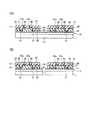
次いで、図3(B)に示すように、ダイシングライン1aに沿って半導体装置を個々のチップに分割する。分割後の半導体装置において、第1の凸部材23は半導体装置の周辺部に位置している。また、第1の凸部材23とパッシベーション膜22の密着性は、ポリイミド樹脂層24とパッシベーション膜22の密着性より高い。このため、第1の凸部材23は、パッシベーション膜22とポリイミド樹脂層24の界面に働く応力を受け止めることができ、パッシベーション膜22とポリイミド樹脂層24の剥離を抑制することができる。 Next, as shown in FIG. 3B, the semiconductor device is divided into individual chips along the dicing
また、第2の凸部材26とポリイミド樹脂層24の密着性は、ソルダーレジスト層27とポリイミド樹脂層24の密着性より高い。このため、第2の凸部材26は、ポリイミド樹脂層24とソルダーレジスト層27の界面に働く応力を受け止めることができ、ポリイミド樹脂層24とソルダーレジスト層27の剥離を抑制することができる。 Further, the adhesion between the second
図4(A)は、第1の凸部材23の平面形状の第1の例を説明する為の平面図である。本例において、第1の凸部材23は、チップ分割後のパッシベーション膜22の周辺部に沿って、ミシン目状に形成されている。また、チップ角部において、第1の凸部材23は略L型になっている。 FIG. 4A is a plan view for explaining a first example of the planar shape of the first
図4(B)は、第1の凸部材23の平面形状の第2の例を説明する為の平面図である。本例において、第1の凸部材23は、図4(A)に示した位置に加えて、複数のAl合金パッド21の相互間にも複数形成されている。この場合、ポリイミド樹脂層24とソルダーレジスト層27は、第1の例よりも剥離しにくくなる。 FIG. 4B is a plan view for explaining a second example of the planar shape of the first
図4(C)は、第1の凸部材23の平面形状の第3の例を説明する為の平面図である。本例において、第1の凸部材23は、チップ分割後のパッシベーション膜22の周辺部に沿って2重に形成されている。一重目、2重目それぞれの第1の凸部材23はミシン目状に形成されているが、互いの空洞部が重ならないように配置されている。この場合、ポリイミド樹脂層24とソルダーレジスト層27は、第1の例よりも剥離しにくくなる。 FIG. 4C is a plan view for explaining a third example of the planar shape of the first
尚、第2の凸部材26の平面形状は、図4(A)〜(C)に示した第1の凸部材23と同一であってもよいが、異なっていてもよい。 Note that the planar shape of the second
以上、第1の実施形態によれば、パッシベーション膜22上に第1の凸部材23を形成したため、パッシベーション膜22とポリイミド樹脂層24の界面に働く応力は、第1の凸部材23によって受け止められ、パッシベーション膜22とポリイミド樹脂層24の剥離を抑制することができる。また、第1の凸部材23はインクジェット機構50を用いて金属ペーストを吐出することにより形成され、ドライエッチング処理が不要になる。このため、第1の凸部材23を形成する際に、Al合金パッド21にはプラズマダメージが加わらない。 As described above, according to the first embodiment, since the first
また、ポリイミド樹脂層24上に第2の凸部材26を形成したため、ポリイミド樹脂層24とソルダーレジスト層27の界面に働く応力は、第2の凸部材26によって受け止められ、ポリイミド樹脂層24とソルダーレジスト層27の剥離を抑制することができる。また、第2の凸部材26は再配線25と同一工程で形成されるため、工程数の増加を抑制することができる。 In addition, since the second
尚、ダイシングライン1a上には、多層配線層10を形成しなくてもよい。このような構成は、例えば、層間絶縁膜それぞれに接続孔を形成するとき、及びAl合金膜をパターニングしてAl合金配線を形成するときそれぞれにおいて、ダイシングライン1a上に位置する層間絶縁膜及びAl合金膜を除去することにより形成される。 Note that the
図5の各図は、本発明の第2の実施形態に係る半導体装置の製造方法を説明する為の断面図である。本実施形態は、第1の凸部材23を形成する方法を除いて、第1の実施形態と同一である。以下、第1の実施形態と同一の構成については同一に符号を付し、第1の凸部材23を形成する工程を除いて説明を省略する。 Each drawing in FIG. 5 is a cross-sectional view for explaining the method for manufacturing a semiconductor device according to the second embodiment of the present invention. This embodiment is the same as the first embodiment except for the method of forming the first
図5(A)に示すように、まず、パッシベーション膜22全面上にフォトレジスト膜を塗布し、このフォトレジスト膜を露光及び現像する。これにより、パッシベーション膜22上にはレジストパターン40が形成される。レジストパターン40は、第1の凸部材23が形成されるべき位置に、開口部40aを有する。 As shown in FIG. 5A, first, a photoresist film is applied over the entire surface of the
次いで、図5(B)に示すように、スキージを用いて開口部40a内に金属ペーストを埋め込み、その後、開口部40a内の金属ペーストを例えば230℃で一時間焼成する。
次いで、図5(C)に示すように、レジストパターン40を除去する。このようにして、第1の凸部材23が形成される。Next, as shown in FIG. 5B, a metal paste is embedded in the
Next, as shown in FIG. 5C, the resist
この第2の実施形態によれば、第1の実施形態と同一の効果を得ることができる。また、複数の第1の凸部材23を同一工程で形成することができるため、半導体装置の生産性が向上する。 According to the second embodiment, the same effect as that of the first embodiment can be obtained. Moreover, since the several 1st
尚、本発明は上述した実施形態に限定されるものではなく、本発明の主旨を逸脱しない範囲内で種々変更して実施することが可能である。例えば、第1及び第2の実施形態において、第2の凸部材26を第1の凸部材23と同一の方法により形成してもよい。このようにすると、第2の凸部材26を再配線25より高くすることができる。
また、第1の凸部材23,26それぞれの形状は、上記した例に限定されるものではなく、例えば格子状、菱型、十字状、スリット状であってもよい。Note that the present invention is not limited to the above-described embodiment, and various modifications can be made without departing from the spirit of the present invention. For example, in the first and second embodiments, the second
Further, the shape of each of the first
1,101…シリコン基板、1a,101a…ダイシングライン、2…素子分離膜、3…ゲート酸化膜、4…ゲート電極、5…サイドウォール、6a,6b…低濃度不純物領域、7a,7b…不純物領域、10,110…多層配線層、11,20…層間絶縁膜、13a,13b,13c…Al合金配線、21,121…Al合金パッド、22,122…パッシベーション膜、23,26…アンカー部材、24,124…ポリイミド樹脂層、24a,27a,40a…開口部、25,125…再配線、27,127…ソルダーレジスト層、28,128…ハンダボール、40…レジストパターン、50…インクジェット機構DESCRIPTION OF SYMBOLS 1,101 ... Silicon substrate, 1a, 101a ... Dicing line, 2 ... Element isolation film, 3 ... Gate oxide film, 4 ... Gate electrode, 5 ... Side wall, 6a, 6b ... Low concentration impurity region, 7a, 7b ...
Claims (3)
Translated fromJapanese前記絶縁膜上に形成されたパッドと、
前記絶縁膜上及びパッド上に形成されたパッシベーション膜と、
前記パッシベーション膜に形成され、前記パッド上に位置する第1の開口部と、
前記パッシベーション膜上に形成された第1の凸部材と、
前記パッシベーション膜上及び前記第1の凸部材上に形成された第1の絶縁層と、
前記第1の絶縁層に形成され、前記第1の開口部上に位置する第2の開口部と、
前記第1の絶縁層上に形成され、前記第1及び第2の開口部を介して前記パッドに接続された再配線と、
前記第1の絶縁層上、及び前記再配線上に形成された第2の絶縁層と、
前記第2の絶縁層に形成され、前記再配線上に位置する第3の開口部と、
前記第3の開口部に埋め込まれ、前記再配線に接続する接続端子と、
前記第1の絶縁層上に形成され、前記第2の絶縁層に覆われた第2の凸部材と、
を具備する半導体装置。An insulating film formed above the semiconductor substrate;
A pad formed on the insulating film;
A passivation film formed on the insulating film and the pad;
A first opening formed in the passivation film and located on the pad;
A first convex member formed on the passivation film;
A first insulating layer formed on the passivation film and on the first convex member;
A second opening formed in the first insulating layer and located on the first opening;
A rewiring formed on the first insulating layer and connected to the pad through the first and second openings;
A second insulating layer formed on the first insulating layer and on the rewiring;
A third opening formed in the second insulating layer and located on the rewiring;
A connection terminal embedded in the third opening and connected to the rewiring;
A second convex member formed on the first insulating layer and covered with the second insulating layer;
A semiconductor device comprising:
前記絶縁膜上に形成されたパッドと、
前記絶縁膜上及び前記パッド上に形成されたパッシベーション膜と、
前記パッシベーション膜に形成され、前記パッド上に位置する第1の開口部と、
前記パッシベーション膜上に形成された第1の絶縁層と、
前記第1の絶縁層に形成され、前記第1の開口部上に位置する第2の開口部と、
前記第1の絶縁層上に形成され、前記第1及び第2の開口部を介して前記パッドに接続する再配線と、
前記第1の絶縁層上に形成された凸部材と、
前記第1の絶縁層上、前記凸部材、及び前記再配線上に形成された第2の絶縁層と、
を具備する半導体装置。An insulating film formed above the semiconductor substrate;
A pad formed on the insulating film;
A passivation film formed on the insulating film and the pad;
A first opening formed in the passivation film and located on the pad;
A first insulating layer formed on the passivation film;
A second opening formed in the first insulating layer and located on the first opening;
A rewiring formed on the first insulating layer and connected to the pad through the first and second openings;
A convex member formed on the first insulating layer;
A second insulating layer formed on the first insulating layer, the convex member, and the rewiring;
A semiconductor device comprising:
前記絶縁膜上にパッドを形成する工程と、
前記絶縁膜上及び前記パッド上にパッシベーション膜を形成する工程と、
前記パッシベーション膜に、前記パッド上に位置する第1の開口部を形成する工程と、
前記パッシベーション膜上に、前記第1の開口部上に第2の開口部を有する第1の絶縁層を形成する工程と、
前記第1の絶縁層上に、前記第1及び第2の開口部を介して前記パッドに接続する再配線、及び凸部材を形成する工程と、
前記第1の絶縁層上、前記再配線上、及び前記凸部材上に、前記再配線上に位置する第3の開口部を有する第2の絶縁層を形成する工程と、
を具備する半導体装置の製造方法。Forming an insulating film above the semiconductor substrate;
Forming a pad on the insulating film;
Forming a passivation film on the insulating film and the pad;
Forming a first opening located on the pad in the passivation film;
Forming a first insulating layer having a second opening on the first opening on the passivation film;
Forming a rewiring connected to the pad via the first and second openings and a convex member on the first insulating layer;
Forming a second insulating layer having a third opening located on the rewiring on the first insulating layer, on the rewiring, and on the convex member;
A method for manufacturing a semiconductor device comprising:
Priority Applications (2)
| Application Number | Priority Date | Filing Date | Title |
|---|---|---|---|
| JP2004309420AJP3976043B2 (en) | 2004-10-25 | 2004-10-25 | Semiconductor device and manufacturing method thereof |
| US11/233,282US20060087040A1 (en) | 2004-10-25 | 2005-09-22 | Semiconductor device and method of manufacturing the same |
Applications Claiming Priority (1)
| Application Number | Priority Date | Filing Date | Title |
|---|---|---|---|
| JP2004309420AJP3976043B2 (en) | 2004-10-25 | 2004-10-25 | Semiconductor device and manufacturing method thereof |
Publications (2)
| Publication Number | Publication Date |
|---|---|
| JP2006120978A JP2006120978A (en) | 2006-05-11 |
| JP3976043B2true JP3976043B2 (en) | 2007-09-12 |
Family
ID=36205479
Family Applications (1)
| Application Number | Title | Priority Date | Filing Date |
|---|---|---|---|
| JP2004309420AExpired - Fee RelatedJP3976043B2 (en) | 2004-10-25 | 2004-10-25 | Semiconductor device and manufacturing method thereof |
Country Status (2)
| Country | Link |
|---|---|
| US (1) | US20060087040A1 (en) |
| JP (1) | JP3976043B2 (en) |
Families Citing this family (6)
| Publication number | Priority date | Publication date | Assignee | Title |
|---|---|---|---|---|
| JP5139039B2 (en)* | 2007-11-20 | 2013-02-06 | 新光電気工業株式会社 | Semiconductor device and manufacturing method thereof |
| US7952187B2 (en)* | 2008-03-31 | 2011-05-31 | General Electric Company | System and method of forming a wafer scale package |
| JP5386852B2 (en)* | 2008-05-07 | 2014-01-15 | 株式会社リコー | Multilayer structure, semiconductor device, method of manufacturing multilayer structure, and method of manufacturing semiconductor device |
| US8766438B2 (en) | 2009-09-01 | 2014-07-01 | Advanpack Solutions Pte Ltd. | Package structure |
| US8246190B2 (en)* | 2010-03-16 | 2012-08-21 | Michael Boiteau | Beverage server tray |
| US9275925B2 (en) | 2013-03-12 | 2016-03-01 | Taiwan Semiconductor Manufacturing Company, Ltd. | System and method for an improved interconnect structure |
Family Cites Families (8)
| Publication number | Priority date | Publication date | Assignee | Title |
|---|---|---|---|---|
| JP3474937B2 (en)* | 1994-10-07 | 2003-12-08 | 株式会社東芝 | Method of manufacturing wiring board for mounting and method of manufacturing semiconductor package |
| EP0734059B1 (en)* | 1995-03-24 | 2005-11-09 | Shinko Electric Industries Co., Ltd. | Chip sized semiconductor device and a process for making it |
| KR100218996B1 (en)* | 1995-03-24 | 1999-09-01 | 모기 쥰이찌 | Semiconductor device |
| JP3629178B2 (en)* | 2000-02-21 | 2005-03-16 | Necエレクトロニクス株式会社 | Flip chip type semiconductor device and manufacturing method thereof |
| US6818545B2 (en)* | 2001-03-05 | 2004-11-16 | Megic Corporation | Low fabrication cost, fine pitch and high reliability solder bump |
| JP3872319B2 (en)* | 2001-08-21 | 2007-01-24 | 沖電気工業株式会社 | Semiconductor device and manufacturing method thereof |
| TWI234253B (en)* | 2002-05-31 | 2005-06-11 | Fujitsu Ltd | Semiconductor device and manufacturing method thereof |
| JP2004055965A (en)* | 2002-07-23 | 2004-02-19 | Seiko Epson Corp | Wiring board, semiconductor device, manufacturing method thereof, circuit board, and electronic equipment |
- 2004
- 2004-10-25JPJP2004309420Apatent/JP3976043B2/ennot_activeExpired - Fee Related
- 2005
- 2005-09-22USUS11/233,282patent/US20060087040A1/ennot_activeAbandoned
Also Published As
| Publication number | Publication date |
|---|---|
| JP2006120978A (en) | 2006-05-11 |
| US20060087040A1 (en) | 2006-04-27 |
Similar Documents
| Publication | Publication Date | Title |
|---|---|---|
| JP4247690B2 (en) | Electronic parts and manufacturing method thereof | |
| US7294933B2 (en) | Semiconductor wafer, semiconductor device and method of manufacturing the same, circuit board, and electronic equipment | |
| US7285867B2 (en) | Wiring structure on semiconductor substrate and method of fabricating the same | |
| CN102456650B (en) | Conductive structure of semiconductor substrate and its manufacturing method | |
| JP6635328B2 (en) | Semiconductor device and method of manufacturing the same | |
| JP2009124042A (en) | Semiconductor device | |
| JP2001077150A (en) | Semiconductor device and method of manufacturing the same | |
| US6639314B2 (en) | Solder bump structure and a method of forming the same | |
| JP2009064897A (en) | Semiconductor device, and its manufacturing method | |
| JP3976043B2 (en) | Semiconductor device and manufacturing method thereof | |
| JP5361264B2 (en) | Semiconductor device | |
| US20080203569A1 (en) | Semiconductor device and manufacturing method thereof | |
| JP2010056266A (en) | Method of manufacturing semiconductor apparatus | |
| US7105433B2 (en) | Method for treating wafer surface | |
| JP2004273592A (en) | Semiconductor device and manufacturing method thereof | |
| JP2005150578A (en) | Semiconductor device and its manufacturing method | |
| JP3915670B2 (en) | Semiconductor device and manufacturing method thereof | |
| JP4145902B2 (en) | Semiconductor device and manufacturing method thereof | |
| JP2006287094A (en) | Semiconductor device and manufacturing method thereof | |
| JP3726906B2 (en) | Semiconductor device and manufacturing method thereof, circuit board, and electronic apparatus | |
| JP2005064193A (en) | Semiconductor device and manufacturing method thereof | |
| TWI849617B (en) | Chip package and manufacturing method thereof | |
| JP2018073968A (en) | Semiconductor device and manufacturing method thereof | |
| TW571419B (en) | Semiconductor device and manufacturing method thereof | |
| JP4099667B2 (en) | Manufacturing method of semiconductor device |
Legal Events
| Date | Code | Title | Description |
|---|---|---|---|
| A977 | Report on retrieval | Free format text:JAPANESE INTERMEDIATE CODE: A971007 Effective date:20070307 | |
| A131 | Notification of reasons for refusal | Free format text:JAPANESE INTERMEDIATE CODE: A131 Effective date:20070313 | |
| A521 | Request for written amendment filed | Free format text:JAPANESE INTERMEDIATE CODE: A523 Effective date:20070507 | |
| TRDD | Decision of grant or rejection written | ||
| A01 | Written decision to grant a patent or to grant a registration (utility model) | Free format text:JAPANESE INTERMEDIATE CODE: A01 Effective date:20070529 | |
| A61 | First payment of annual fees (during grant procedure) | Free format text:JAPANESE INTERMEDIATE CODE: A61 Effective date:20070611 | |
| FPAY | Renewal fee payment (event date is renewal date of database) | Free format text:PAYMENT UNTIL: 20100629 Year of fee payment:3 | |
| R150 | Certificate of patent or registration of utility model | Free format text:JAPANESE INTERMEDIATE CODE: R150 | |
| FPAY | Renewal fee payment (event date is renewal date of database) | Free format text:PAYMENT UNTIL: 20110629 Year of fee payment:4 | |
| FPAY | Renewal fee payment (event date is renewal date of database) | Free format text:PAYMENT UNTIL: 20110629 Year of fee payment:4 | |
| FPAY | Renewal fee payment (event date is renewal date of database) | Free format text:PAYMENT UNTIL: 20120629 Year of fee payment:5 | |
| FPAY | Renewal fee payment (event date is renewal date of database) | Free format text:PAYMENT UNTIL: 20130629 Year of fee payment:6 | |
| FPAY | Renewal fee payment (event date is renewal date of database) | Free format text:PAYMENT UNTIL: 20130629 Year of fee payment:6 | |
| LAPS | Cancellation because of no payment of annual fees |