JP3973082B2 - Double-sided LED package - Google Patents
Double-sided LED packageDownload PDFInfo
- Publication number
- JP3973082B2 JP3973082B2JP2002024811AJP2002024811AJP3973082B2JP 3973082 B2JP3973082 B2JP 3973082B2JP 2002024811 AJP2002024811 AJP 2002024811AJP 2002024811 AJP2002024811 AJP 2002024811AJP 3973082 B2JP3973082 B2JP 3973082B2
- Authority
- JP
- Japan
- Prior art keywords
- circuit board
- reflective cup
- led package
- led
- electrode
- Prior art date
- Legal status (The legal status is an assumption and is not a legal conclusion. Google has not performed a legal analysis and makes no representation as to the accuracy of the status listed.)
- Expired - Fee Related
Links
Images


Classifications
- H—ELECTRICITY
- H10—SEMICONDUCTOR DEVICES; ELECTRIC SOLID-STATE DEVICES NOT OTHERWISE PROVIDED FOR
- H10H—INORGANIC LIGHT-EMITTING SEMICONDUCTOR DEVICES HAVING POTENTIAL BARRIERS
- H10H20/00—Individual inorganic light-emitting semiconductor devices having potential barriers, e.g. light-emitting diodes [LED]
- H10H20/80—Constructional details
- H10H20/85—Packages
- H10H20/8506—Containers
- H—ELECTRICITY
- H01—ELECTRIC ELEMENTS
- H01L—SEMICONDUCTOR DEVICES NOT COVERED BY CLASS H10
- H01L25/00—Assemblies consisting of a plurality of semiconductor or other solid state devices
- H01L25/03—Assemblies consisting of a plurality of semiconductor or other solid state devices all the devices being of a type provided for in a single subclass of subclasses H10B, H10D, H10F, H10H, H10K or H10N, e.g. assemblies of rectifier diodes
- H01L25/04—Assemblies consisting of a plurality of semiconductor or other solid state devices all the devices being of a type provided for in a single subclass of subclasses H10B, H10D, H10F, H10H, H10K or H10N, e.g. assemblies of rectifier diodes the devices not having separate containers
- H01L25/075—Assemblies consisting of a plurality of semiconductor or other solid state devices all the devices being of a type provided for in a single subclass of subclasses H10B, H10D, H10F, H10H, H10K or H10N, e.g. assemblies of rectifier diodes the devices not having separate containers the devices being of a type provided for in group H10H20/00
- H01L25/0756—Stacked arrangements of devices
- H—ELECTRICITY
- H01—ELECTRIC ELEMENTS
- H01L—SEMICONDUCTOR DEVICES NOT COVERED BY CLASS H10
- H01L2224/00—Indexing scheme for arrangements for connecting or disconnecting semiconductor or solid-state bodies and methods related thereto as covered by H01L24/00
- H01L2224/01—Means for bonding being attached to, or being formed on, the surface to be connected, e.g. chip-to-package, die-attach, "first-level" interconnects; Manufacturing methods related thereto
- H01L2224/10—Bump connectors; Manufacturing methods related thereto
- H01L2224/15—Structure, shape, material or disposition of the bump connectors after the connecting process
- H01L2224/16—Structure, shape, material or disposition of the bump connectors after the connecting process of an individual bump connector
- H01L2224/161—Disposition
- H01L2224/16151—Disposition the bump connector connecting between a semiconductor or solid-state body and an item not being a semiconductor or solid-state body, e.g. chip-to-substrate, chip-to-passive
- H01L2224/16221—Disposition the bump connector connecting between a semiconductor or solid-state body and an item not being a semiconductor or solid-state body, e.g. chip-to-substrate, chip-to-passive the body and the item being stacked
- H01L2224/16225—Disposition the bump connector connecting between a semiconductor or solid-state body and an item not being a semiconductor or solid-state body, e.g. chip-to-substrate, chip-to-passive the body and the item being stacked the item being non-metallic, e.g. insulating substrate with or without metallisation
- H—ELECTRICITY
- H01—ELECTRIC ELEMENTS
- H01L—SEMICONDUCTOR DEVICES NOT COVERED BY CLASS H10
- H01L25/00—Assemblies consisting of a plurality of semiconductor or other solid state devices
- H01L25/03—Assemblies consisting of a plurality of semiconductor or other solid state devices all the devices being of a type provided for in a single subclass of subclasses H10B, H10D, H10F, H10H, H10K or H10N, e.g. assemblies of rectifier diodes
- H01L25/04—Assemblies consisting of a plurality of semiconductor or other solid state devices all the devices being of a type provided for in a single subclass of subclasses H10B, H10D, H10F, H10H, H10K or H10N, e.g. assemblies of rectifier diodes the devices not having separate containers
- H01L25/075—Assemblies consisting of a plurality of semiconductor or other solid state devices all the devices being of a type provided for in a single subclass of subclasses H10B, H10D, H10F, H10H, H10K or H10N, e.g. assemblies of rectifier diodes the devices not having separate containers the devices being of a type provided for in group H10H20/00
- H01L25/0753—Assemblies consisting of a plurality of semiconductor or other solid state devices all the devices being of a type provided for in a single subclass of subclasses H10B, H10D, H10F, H10H, H10K or H10N, e.g. assemblies of rectifier diodes the devices not having separate containers the devices being of a type provided for in group H10H20/00 the devices being arranged next to each other
Landscapes
- Engineering & Computer Science (AREA)
- Power Engineering (AREA)
- Microelectronics & Electronic Packaging (AREA)
- Physics & Mathematics (AREA)
- Condensed Matter Physics & Semiconductors (AREA)
- General Physics & Mathematics (AREA)
- Computer Hardware Design (AREA)
- Telephone Set Structure (AREA)
- Led Device Packages (AREA)
Description
Translated fromJapanese【0001】
【発明の属する技術分野】
本発明は、パーソナルコンピューター、プリンター、PDA、ファクシミリ、ページャー、携帯電話等の民生機器に使用される両面発光LEDパッケージに関する。
【0002】
【従来の技術】
近年、光通信機能を搭載したノート型パソコン、PDA、携帯電話等の携帯機器などの各種電子機器の表示装置として、薄型で見やすいバックライト機構を備えた液晶表示装置が広く用いられている。従来のこのようなLCDを備えた電子機器として、携帯電話のLCDバックライト、各種キー照明兼用のLEDパッケージについて説明する。
【0003】
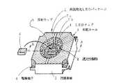
図7は、一般的に使用されている携帯電話の正面図である。図7において、10はケース本体で、その上側には略長方形をしたLCD11が配設されている。12はLCDバックライト用のLEDパッケージで、1〜4個程度(図7では3個)使用している。また、ケース本体10の下側には、複数個の操作用のキースイッチ13が配設されていて、これらのキースイッチ13のバックライト用として、4〜20個程度(図7では16個)の多数のLEDパッケージ12が使用されている。
【0004】
現状使用されているLEDパッケージ(図示せず)は、例えば、略四角形状をしたガラスエポキシ樹脂などよりなる絶縁回路基板の四隅にスルーホール電極(側面電極)を形成し、該スルーホール電極で回路基板に形成された上、下面電極に接続する。そして前記回路基板の略中央部に設けた反射カップの底部にLEDップを実装し、このLEDチップを覆うように透光性樹脂を充填する。
【0005】
【発明が解決しようとする課題】
上記した上面発光タイプのLEDパッケージや、側面発光タイプのLEDパッケージなどでは、光の指向特性上多数のLEDパッケージを使用しなければならないと言う問題があった。
【0006】
本発明は上記従来の課題に鑑みなされたものであり、その目的は、LEDパッケージの使用個数を低減させ、また1つのLEDパッケージで、表、裏に異なる種類のLEDチップを実装可能にした、安価な両面発光LEDパッケージを提供するものである。
【0007】
【課題を解決するための手段】
上記目的を達成するために、本発明における両面発光LEDパッケージは、略四角形状をした絶縁性を有する回路基板の表面と裏面の各々にLEDチップを収納する反射カップと前記回路基板の四隅に有底ホールとを形成し、前記反射カップを含み前記回路基板の表裏両面に平面を二分するように電極パターンを形成すると共に、前記有底ホール内に前記電極パターンと電気的に接続するように前記LEDチップ実装時の電極端子となるパターンを形成して、前記反射カップの底面に前記電極パターンを跨ぐように前記LEDチップをフリップチップ実装し、更に前記反射カップ内に透光性樹脂を充填し、且つ、前記回路基板へ側面電極やスルーホールを形成しないことによって前記回路基板の表面と裏面の電極パターンを電気的に分離し、前記回路基板の表面と裏面の両面から光を発光させることを特徴とするものである。
【0008】
また、本発明における両面発光LEDパッケージは、略四角形状をした絶縁性を有する回路基板の表面と裏面の各々にLEDチップを収納する反射カップと前記回路基板の四隅に有底ホールとを形成し、前記反射カップを含み前記回路基板の表裏両面に平面を二分するように電極パターンを形成すると共に、前記有底ホール内に前記電極パターンと電気的に接続するように前記LEDチップ実装時の電極端子となるパターンを形成して、前記反射カップの底面に前記電極パターンを跨ぐように前記LEDチップをフリップチップ実装し、更に前記反射カップ内上の前記回路基板面にガラス又は樹脂等の透明シートを貼付し、且つ、前記回路基板へ側面電極やスルーホールを形成しないことによって前記回路基板の表面と裏面の電極パターンを電気的に分離し、前記回路基板の表面と裏面の両面から光を発光させることを特徴とするものである。
【0009】
また、前記回路基板に形成された反射カップ内に充填する透光性樹脂に、蛍光剤を混入したことを特徴とするものである。
【0010】
また、前記回路基板面に貼付するガラス又は樹脂等の透明シート内に、蛍光剤を混入したことを特徴とするものである。
【0011】
また、前記回路基板の表面と裏面に形成された反射カップの底面に、異なる種類のLEDチップをフリップチップ実装したことを特徴とするものである。
【0012】
【発明の実施の形態】
以下、図面に基づいて本発明における両面発光LEDパッケージについて説明する。図1及び図2は、本発明の第1の実施の形態に係わり、図1は、両面発光LEDパッケージの斜視図、図2は、図1のA−A線断面図である。
【0013】
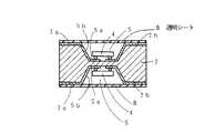
図1及び図2において、1は両面発光LEDパッケージであり、その構成は、略四角形状をしたガラスエポキシ樹脂などよりなる絶縁性を有する回路基板2の表面と裏面とが対称になるように、前記回路基板2の四隅に有底ホール3(略四分の一程度)が形成されていて、略中央部にLEDチップ4を収納する反射カップ5が形成されている。前記回路基板2に形成された有底ホール3にはLED実装時の電極端子6を形成すると共に、前記反射カップ5の底面5a及び斜面部5bを含み回路基板2の平面を二分するように電極パターン7a、7bを形成する。更に、前記反射カップ5の底面5aにおいて、前記電極パターン7a、7bを跨ぐようにLEDチップ4をフリップチップ実装する。前記反射カップ5の底面5a及び斜面部5bには、電極形成時のAg又はAuメッキ部が設けられる。そして、LEDチップ4を実装した後、反射カップ5の凹部内に透光性樹脂8を充填する。
【0014】
また、充填する透光性樹脂8内に蛍光剤等を混入することにより、色調変換の機能を実現することも可能である。
【0015】
以上述べたように、回路基板2の表面と裏面とが対称に構成されている。回路基板2の四隅に形成した電極端子6は貫通スルーホール電極でないので、表と裏の電極が分離されるため、両面発光のLEDパッケージを実現することができる。更に、4端子の電極端子6に、表と裏で印加する電圧を変えることができ、4元系、GaN系等の異なる種類のLEDを実装することができる。また、反射カップ5の斜面部5bにはAg又はAuメッキ部などの反射薄膜が施されているので反射効率を良くすることができる。
【0016】
図3は、本発明の第2の実施の形態に係わる両面発光LEDパッケージの断面図である。図3に示す両面発光LEDパッケージ1Aにおいて、上述した第1の実施の形態で説明した両面発光LEDパッケージと異なるところは、前記回路基板2に形成された反射カップ5の底面5aにLEDチップ4を実装した後、反射カップ5内に透光性樹脂を充填しないで、前記反射カップ5内に空気層を有する状態で、回路基板2の面にガラス又は樹脂等の透明シート9を貼付したものである。
【0017】
また、貼付する透明シート9は、樹脂等に蛍光剤を混入し、シート状に成形したものを用いることにより、色調変換の機能を実現することも可能である。
【0018】
ここで、前記両面発光LEDパッケージの製造方法について説明する。図4は、集合基板の斜視図である。図4において、2Aは、多数個取りするガラスエポキシ樹脂等よりなる集合基板で、該集合基板2Aの表面と裏面が対称になるように、集合基板2Aの平面上に格子状に配列するように複数個の有底ホール3を複数列配設する。更に、各列間の略中央部にLEDチップ4を収納する反射カップ5を配設する。前記有底ホール3は、直交するカットラインX上に形成されて電極端子部になる。
【0019】
前記集合基板2Aに電極パターンを形成するには、集合基板2Aの表、裏面にAg又はAuメッキ処理を施し、メッキレジストを付加し、パターンマスクにより露光現像し、パターンエッチングを行い、前記集合基板2Aに電極パターン7a、7bと、前記有底ホール3内にLED実装時の電極端子6を形成する。
【0020】
図示しないが、更に、前記集合基板2A上の個々の反射カップ5の底面5aにおいて、前記電極パターン7a、7bを跨ぐようにLEDチップ4をフリップチップ実装する。前述したように、反射カップ5の凹部内に透光性樹脂(図1、2)を充填するか、樹脂を充填しない場合はガラス又は樹脂等の透明シート(図3)を貼付した後、集合基板2Aに形成された有底ホール3の略中心部を通る直交するカットラインXに沿って切断して、図1、2又は図3に示す単個の両面発光LEDパッケージ1又は1Aに分割する。
【0021】
前述したように、色調変換の機能を実現するために、充填する透光性樹脂に蛍光剤を混入するか、または、貼付する透明シートは樹脂等に蛍光剤を混入してシート状に成形したものを用いる。
【0022】
上記したように、集合基板により両面発光LEDパッケージを多数個取り生産が可能でコストダウンとなる。
【0023】
以上述べた構成による作用・効果は、1個のパッケージで表、裏両面発光が可能である。また、表面と裏面に異なる種類のLEDが実装できる。更に、蛍光剤等で波長変換し色調を変えることもできる。
【0024】
ここで、上記した両面発光LEDパッケージを携帯電話に使用した応用例について説明する。図5は、両面発光LEDパッケージを使用した携帯電話の正面図、図6は、図5のB−B線断面図である。図5において、10はケース本体で、その上側には略長方形をしたLCD11が配設されて、下側には複数個の操作用のキースイッチ13が配設されていて、後述するLCD部導光板とキースイッチ部導光板との間に本発明の両面発光LEDパッケージ1(又は1A)を1〜3個程度(図5では3個)使用している。この両面発光LEDパッケージ1(又は1A)でLCDバックライト用とキースイッチ部バックライト用とを兼用するものである。
【0025】
図6において、前記両面発光LEDパッケージ1Aは、1個のLEDパッケージで両面が発光する。例えば、一方のLEDチップ4Aはキースイッチ部導光板14A方向に出射して、キースイッチ部バックライト用として機能する。また、他方のLEDチップ4BはLCD部導光板14B方向に出射して、LCD部バックライト用として機能する。
【0026】
以上述べたように、両面発光LEDパッケージを携帯電話に使用することにより、従来、多数使用していたLEDパッケージの数量を大幅に低減することができる。
【0027】
また、一般的には、LCD部バックライト用としては白色、キースイッチ部バックライト用としては緑色を発光するように、異なる種類のLEDチップを実装して、1つのパッケージで異なる色を発光させることが可能である。
【0028】
【発明の効果】
以上説明したように、本発明によれば、1つのパッケージで両面発光LEDパッケージを実現することが可能である。従来、多数使用していたLEDパッケージの数量を大幅に低減しコストダウンが図られる。また、1つのパッケージで表、裏に異なる種類のLEDチップを実装することができる。更に、蛍光剤等で色調変換し所望の色を発光させることができる等、優れた両面発光LEDパッケージを提供することがであきる。
【図面の簡単な説明】
【図1】本発明の第1の実施の形態に係わる両面発光LEDパッケージの斜視図である。
【図2】図1のA−A線断面図である。
【図3】本発明の第2の実施の形態に係わる両面発光LEDパッケージの断面図である。
【図4】図1、図3の両面発光LEDパッケージの製造方法を説明する集合基板の斜視図である。
【図5】図1の両面発光LEDパッケージを使用した携帯電話の正面図である。
【図6】図4のB−B線断面図である。
【図7】従来の上面発光LEDパッケージを使用した携帯電話の正面図である。
【符号の説明】
1、1A 両面発光LEDパッケージ
2 回路基板
2A 集合基板
3 有底ホール
4、4A、4B LEDチップ
5 反射カップ
5a 底面
5b 反射面部
6 電極端子
7a、7b 電極パターン
8 透光性樹脂
9 透明シート
10 ケース本体
11 LCD
12 LEDパッケージ
13 キースイッチ
14A キースイッチ部導光板
14B LCD部導光板[0001]
BACKGROUND OF THE INVENTION
The present invention relates to a double-sided light emitting LED package used for consumer devices such as personal computers, printers, PDAs, facsimiles, pagers, and mobile phones.
[0002]
[Prior art]
In recent years, a liquid crystal display device having a thin and easy-to-see backlight mechanism has been widely used as a display device of various electronic devices such as notebook personal computers equipped with optical communication functions, PDAs, and mobile phones. As a conventional electronic apparatus equipped with such an LCD, an LCD backlight for a mobile phone and an LED package for various key illumination will be described.
[0003]
FIG. 7 is a front view of a commonly used mobile phone. In FIG. 7,
[0004]
An LED package (not shown) that is currently used has through-hole electrodes (side electrodes) formed at four corners of an insulating circuit board made of, for example, a substantially rectangular glass epoxy resin, and the circuit is formed by the through-hole electrodes. Connected to the lower electrode formed on the substrate. Then, an LED chip is mounted on the bottom of the reflection cup provided at the substantially central portion of the circuit board, and a translucent resin is filled so as to cover the LED chip.
[0005]
[Problems to be solved by the invention]
The above-described top emission type LED package, side emission type LED package, and the like have a problem in that a large number of LED packages must be used due to the light directivity.
[0006]
The present invention has been made in view of the above-described conventional problems, and its purpose is to reduce the number of LED packages used, and to allow different types of LED chips to be mounted on the front and back of one LED package. An inexpensive double-sided light emitting LED package is provided.
[0007]
[Means for Solving the Problems]
In order to achieve the above object, the double-sided light emitting LED package according to the present invention has a reflection cup for storing LED chips on each of the front and back surfaces of asubstantially square-shaped insulatingcircuit board and four corners of the circuit board. a bottom hole is formed, wherein on both sides ofthe circuit board includes a reflective cup and forming an electrode pattern so as to bisect the plane, said to the electrode pattern electrically connected to the bottomed hole A pattern to be an electrode terminal at the time of mounting the LED chip is formed, the LED chip is flip-chip mounted on the bottom surface of the reflective cup so as to straddle the electrode pattern, and a transparent resin is filled in the reflective cup. And electrically separating the electrode patterns on the front and back surfaces of the circuit board by not forming side electrodes or through holes in the circuit board, It is characterized in that emit light from both sides of the front and back of the serial circuit board.
[0008]
Further, the double-sided light emitting LED package according to the present invention is formed by forming a reflective cup for storing the LED chip on eachof the front and back surfaces of the circuit board havinga substantially rectangular shape and the bottomed holes atthe four corners of the circuit board. , thereby forming an electrode pattern so as to divide the plane on both sides ofthe circuit board comprises the reflective cup, wherein the LED chip during mounting electrodes to the electrode pattern electrically connected to the bottomed hole A pattern to be a terminal is formed, the LED chip is flip-chip mounted on the bottom surface of the reflective cup so as to straddle the electrode pattern, and a transparent sheet such as glass or resin is further formed on the circuit board surface on the reflective cup And the electrode patterns on the front and back surfaces of the circuit board are not formed by forming side electrodes or through holes on the circuit board. Air to separate, is characterized in that emit light from both sides of the front and rear surfaces of the circuit board.
[0009]
In addition, a fluorescent agent is mixed in a translucent resin filled in a reflection cup formed on the circuit board.
[0010]
In addition, a fluorescent agent is mixed in a transparent sheet such as glass or resin to be attached to the circuit board surface.
[0011]
Further, different types of LED chips are flip-chip mounted on the bottom surfaces of the reflection cups formed on the front and back surfaces of the circuit board.
[0012]
DETAILED DESCRIPTION OF THE INVENTION
Hereinafter, a double-sided light emitting LED package according to the present invention will be described with reference to the drawings. 1 and 2 relate to a first embodiment of the present invention, FIG. 1 is a perspective view of a double-sided light emitting LED package, and FIG. 2 is a cross-sectional view taken along line AA of FIG.
[0013]
1 and 2,
[0014]
Moreover, it is also possible to realize a color tone conversion function by mixing a fluorescent agent or the like in the
[0015]
As described above, the front surface and the back surface of the
[0016]
FIG. 3 is a sectional view of a double-sided light emitting LED package according to the second embodiment of the present invention. In the double-sided light emitting
[0017]
In addition, the
[0018]
Here, a method for manufacturing the double-sided light emitting LED package will be described. FIG. 4 is a perspective view of the collective substrate. In FIG. 4, 2A is a collective substrate made of a large number of glass epoxy resins or the like, and is arranged in a grid pattern on the plane of the collective substrate 2A so that the front and back surfaces of the collective substrate 2A are symmetrical. A plurality of bottomed
[0019]
In order to form an electrode pattern on the aggregate substrate 2A, Ag or Au plating treatment is applied to the front and back surfaces of the aggregate substrate 2A, a plating resist is added, exposure and development is performed using a pattern mask, pattern etching is performed, and the aggregate substrate is formed.
[0020]
Although not shown, the
[0021]
As described above, in order to realize the function of color tone conversion, a fluorescent agent is mixed in a translucent resin to be filled, or a transparent sheet to be pasted is formed into a sheet shape by mixing a fluorescent agent in a resin or the like. Use things.
[0022]
As described above, a large number of double-sided light emitting LED packages can be obtained and produced by the collective substrate, thereby reducing the cost.
[0023]
The operations and effects of the above-described configuration allow both front and back side light emission with a single package. Different types of LEDs can be mounted on the front and back surfaces. Further, the color tone can be changed by wavelength conversion with a fluorescent agent or the like.
[0024]
Here, an application example in which the above-described double-sided light emitting LED package is used in a mobile phone will be described. FIG. 5 is a front view of a mobile phone using a double-sided light emitting LED package, and FIG. 6 is a cross-sectional view taken along line BB in FIG. In FIG. 5,
[0025]
In FIG. 6, the double-sided light emitting
[0026]
As described above, by using a double-sided light emitting LED package for a mobile phone, the number of LED packages that have been used in the past can be greatly reduced.
[0027]
Also, in general, different types of LED chips are mounted so that different colors are emitted by one package so that white is emitted for LCD backlight and green is emitted for key switch backlight. It is possible.
[0028]
【The invention's effect】
As described above, according to the present invention, it is possible to realize a double-sided light emitting LED package with a single package. Conventionally, the number of LED packages that have been used in large numbers can be greatly reduced, and the cost can be reduced. Also, different types of LED chips can be mounted on the front and back in one package. Furthermore, it is possible to provide an excellent double-sided light emitting LED package, such as being able to emit a desired color by changing the color tone with a fluorescent agent.
[Brief description of the drawings]
FIG. 1 is a perspective view of a double-sided light emitting LED package according to a first embodiment of the present invention.
FIG. 2 is a cross-sectional view taken along line AA in FIG.
FIG. 3 is a cross-sectional view of a double-sided light emitting LED package according to a second embodiment of the present invention.
4 is a perspective view of a collective substrate for explaining a method of manufacturing the double-sided light emitting LED package of FIGS. 1 and 3. FIG.
5 is a front view of a mobile phone using the double-sided light emitting LED package of FIG. 1. FIG.
6 is a cross-sectional view taken along line BB in FIG.
FIG. 7 is a front view of a mobile phone using a conventional top-emitting LED package.
[Explanation of symbols]
DESCRIPTION OF
12
Claims (5)
Translated fromJapanesePriority Applications (2)
| Application Number | Priority Date | Filing Date | Title |
|---|---|---|---|
| JP2002024811AJP3973082B2 (en) | 2002-01-31 | 2002-01-31 | Double-sided LED package |
| US10/349,028US6876149B2 (en) | 2002-01-31 | 2003-01-23 | Double-face LED device for an electronic instrument |
Applications Claiming Priority (1)
| Application Number | Priority Date | Filing Date | Title |
|---|---|---|---|
| JP2002024811AJP3973082B2 (en) | 2002-01-31 | 2002-01-31 | Double-sided LED package |
Publications (2)
| Publication Number | Publication Date |
|---|---|
| JP2003229603A JP2003229603A (en) | 2003-08-15 |
| JP3973082B2true JP3973082B2 (en) | 2007-09-05 |
Family
ID=27606466
Family Applications (1)
| Application Number | Title | Priority Date | Filing Date |
|---|---|---|---|
| JP2002024811AExpired - Fee RelatedJP3973082B2 (en) | 2002-01-31 | 2002-01-31 | Double-sided LED package |
Country Status (2)
| Country | Link |
|---|---|
| US (1) | US6876149B2 (en) |
| JP (1) | JP3973082B2 (en) |
Families Citing this family (72)
| Publication number | Priority date | Publication date | Assignee | Title |
|---|---|---|---|---|
| JP3838964B2 (en) | 2002-03-13 | 2006-10-25 | 株式会社リコー | Functional element substrate manufacturing equipment |
| DE10255932A1 (en)* | 2002-11-29 | 2004-06-17 | Osram Opto Semiconductors Gmbh | Optoelectronic component |
| JP3716252B2 (en)* | 2002-12-26 | 2005-11-16 | ローム株式会社 | Light emitting device and lighting device |
| USD520965S1 (en)* | 2003-01-10 | 2006-05-16 | Citizen Electronics Co., Ltd. | Light emitting diode for illuminating an object |
| US7675231B2 (en)* | 2004-02-13 | 2010-03-09 | Avago Technologies Ecbu Ip (Singapore) Pte. Ltd. | Light emitting diode display device comprising a high temperature resistant overlay |
| JP4572312B2 (en)* | 2004-02-23 | 2010-11-04 | スタンレー電気株式会社 | LED and manufacturing method thereof |
| US7964883B2 (en)* | 2004-02-26 | 2011-06-21 | Lighting Science Group Corporation | Light emitting diode package assembly that emulates the light pattern produced by an incandescent filament bulb |
| JP2005244076A (en)* | 2004-02-27 | 2005-09-08 | Matsushita Electric Works Ltd | Light-emitting device |
| TWI241034B (en) | 2004-05-20 | 2005-10-01 | Lighthouse Technology Co Ltd | Light emitting diode package |
| US20060006792A1 (en)* | 2004-07-09 | 2006-01-12 | Eastman Kodak Company | Flat panel light emitting devices with two sided |
| US7745832B2 (en)* | 2004-09-24 | 2010-06-29 | Epistar Corporation | Semiconductor light-emitting element assembly with a composite substrate |
| US7821023B2 (en)* | 2005-01-10 | 2010-10-26 | Cree, Inc. | Solid state lighting component |
| US9070850B2 (en) | 2007-10-31 | 2015-06-30 | Cree, Inc. | Light emitting diode package and method for fabricating same |
| US9793247B2 (en)* | 2005-01-10 | 2017-10-17 | Cree, Inc. | Solid state lighting component |
| KR100593935B1 (en)* | 2005-03-24 | 2006-06-30 | 삼성전기주식회사 | Light emitting diode package and manufacturing method thereof |
| US8669572B2 (en)* | 2005-06-10 | 2014-03-11 | Cree, Inc. | Power lamp package |
| JP4715422B2 (en)* | 2005-09-27 | 2011-07-06 | 日亜化学工業株式会社 | Light emitting device |
| US8044412B2 (en) | 2006-01-20 | 2011-10-25 | Taiwan Semiconductor Manufacturing Company, Ltd | Package for a light emitting element |
| US7675145B2 (en) | 2006-03-28 | 2010-03-09 | Cree Hong Kong Limited | Apparatus, system and method for use in mounting electronic elements |
| US8748915B2 (en)* | 2006-04-24 | 2014-06-10 | Cree Hong Kong Limited | Emitter package with angled or vertical LED |
| US7635915B2 (en)* | 2006-04-26 | 2009-12-22 | Cree Hong Kong Limited | Apparatus and method for use in mounting electronic elements |
| WO2007138677A1 (en)* | 2006-05-30 | 2007-12-06 | Fujikura Ltd. | Porcelain substrate for mounting light emitting element, and light source device |
| TWM303493U (en)* | 2006-07-21 | 2006-12-21 | Lighthouse Technology Co Ltd | Support rack structure and metal support rack of side light source SMD LED |
| US8735920B2 (en) | 2006-07-31 | 2014-05-27 | Cree, Inc. | Light emitting diode package with optical element |
| US8367945B2 (en)* | 2006-08-16 | 2013-02-05 | Cree Huizhou Opto Limited | Apparatus, system and method for use in mounting electronic elements |
| JP2010512662A (en) | 2006-12-11 | 2010-04-22 | ザ リージェンツ オブ ザ ユニバーシティ オブ カリフォルニア | Transparent light emitting diode |
| KR101374894B1 (en)* | 2006-12-29 | 2014-03-17 | 서울반도체 주식회사 | Double-side emitting type light emitting diode package |
| USD566059S1 (en)* | 2007-01-05 | 2008-04-08 | Rohm Co., Ltd. | Light emitting diode module |
| US9711703B2 (en)* | 2007-02-12 | 2017-07-18 | Cree Huizhou Opto Limited | Apparatus, system and method for use in mounting electronic elements |
| CN101388161A (en)* | 2007-09-14 | 2009-03-18 | 科锐香港有限公司 | LED surface mounting device and LED display incorporating the same |
| WO2009038072A1 (en)* | 2007-09-21 | 2009-03-26 | Showa Denko K.K. | Light-emitting device, display, and light-emitting device manufacturing method |
| US10256385B2 (en) | 2007-10-31 | 2019-04-09 | Cree, Inc. | Light emitting die (LED) packages and related methods |
| USD615504S1 (en) | 2007-10-31 | 2010-05-11 | Cree, Inc. | Emitter package |
| US8866169B2 (en)* | 2007-10-31 | 2014-10-21 | Cree, Inc. | LED package with increased feature sizes |
| USD633631S1 (en) | 2007-12-14 | 2011-03-01 | Cree Hong Kong Limited | Light source of light emitting diode |
| TWI415293B (en)* | 2007-12-14 | 2013-11-11 | Advanced Optoelectronic Tech | Photoelectric element manufacturing method and package structure thereof |
| USD634863S1 (en) | 2008-01-10 | 2011-03-22 | Cree Hong Kong Limited | Light source of light emitting diode |
| US8049230B2 (en)* | 2008-05-16 | 2011-11-01 | Cree Huizhou Opto Limited | Apparatus and system for miniature surface mount devices |
| CN101319760B (en)* | 2008-06-25 | 2010-12-15 | 吴裕朝 | Light emitting system |
| ATE490444T1 (en)* | 2008-08-27 | 2010-12-15 | Panasonic Corp | COOLING SYSTEM |
| US9425172B2 (en)* | 2008-10-24 | 2016-08-23 | Cree, Inc. | Light emitter array |
| US8791471B2 (en) | 2008-11-07 | 2014-07-29 | Cree Hong Kong Limited | Multi-chip light emitting diode modules |
| JP5324894B2 (en)* | 2008-11-21 | 2013-10-23 | パナソニック株式会社 | Semiconductor device and manufacturing method thereof |
| US8251543B2 (en)* | 2008-11-22 | 2012-08-28 | Innovative Lighting, Inc. | Interior corner mounting module for rope light system |
| US8368112B2 (en)* | 2009-01-14 | 2013-02-05 | Cree Huizhou Opto Limited | Aligned multiple emitter package |
| US8723062B2 (en)* | 2009-02-26 | 2014-05-13 | Blackberry Limited | Key assembly for a handheld electronic device having a one-piece keycap |
| US8263887B2 (en)* | 2009-02-26 | 2012-09-11 | Research In Motion Limited | Backlit key assembly having a reduced thickness |
| US8415692B2 (en)* | 2009-07-06 | 2013-04-09 | Cree, Inc. | LED packages with scattering particle regions |
| US8598809B2 (en)* | 2009-08-19 | 2013-12-03 | Cree, Inc. | White light color changing solid state lighting and methods |
| CN102045910A (en)* | 2009-10-09 | 2011-05-04 | 鸿富锦精密工业(深圳)有限公司 | Light-emitting diode (LED) lighting device |
| CN102148312B (en)* | 2010-02-05 | 2015-01-07 | 亿光电子工业股份有限公司 | Light emitting diode packaging structure, manufacturing method thereof and display device |
| WO2011107925A1 (en)* | 2010-03-03 | 2011-09-09 | Koninklijke Philips Electronics N.V. | Electric lamp having reflector for transferring heat from light source |
| CN102194801A (en)* | 2010-03-04 | 2011-09-21 | 展晶科技(深圳)有限公司 | Packaging structure of light-emitting diode emitting light in forward direction and formation method thereof |
| US9012938B2 (en) | 2010-04-09 | 2015-04-21 | Cree, Inc. | High reflective substrate of light emitting devices with improved light output |
| CN102339819B (en)* | 2010-07-28 | 2014-09-24 | 展晶科技(深圳)有限公司 | Light emitting diode packaging structure and forming method thereof |
| US8210716B2 (en)* | 2010-08-27 | 2012-07-03 | Quarkstar Llc | Solid state bidirectional light sheet for general illumination |
| US8198109B2 (en) | 2010-08-27 | 2012-06-12 | Quarkstar Llc | Manufacturing methods for solid state light sheet or strip with LEDs connected in series for general illumination |
| US8419203B1 (en)* | 2010-09-03 | 2013-04-16 | Rockwell Collins, Inc. | Single card multi mode LCD backlight |
| US8192051B2 (en)* | 2010-11-01 | 2012-06-05 | Quarkstar Llc | Bidirectional LED light sheet |
| US8410726B2 (en) | 2011-02-22 | 2013-04-02 | Quarkstar Llc | Solid state lamp using modular light emitting elements |
| US8314566B2 (en) | 2011-02-22 | 2012-11-20 | Quarkstar Llc | Solid state lamp using light emitting strips |
| CN102856468B (en)* | 2011-06-30 | 2015-02-04 | 展晶科技(深圳)有限公司 | Light emitting diode packaging structure and manufacturing method thereof |
| KR20130014197A (en)* | 2011-07-29 | 2013-02-07 | 엘지이노텍 주식회사 | The light emitting device package and the light emitting system |
| US8564004B2 (en) | 2011-11-29 | 2013-10-22 | Cree, Inc. | Complex primary optics with intermediate elements |
| WO2013115379A1 (en) | 2012-02-02 | 2013-08-08 | シチズンホールディングス株式会社 | Semiconductor light emitting device and fabrication method for same |
| JP6209874B2 (en)* | 2012-08-31 | 2017-10-11 | 日亜化学工業株式会社 | Light emitting device and manufacturing method thereof |
| WO2014040412A1 (en)* | 2012-09-17 | 2014-03-20 | 中国科学院福建物质结构研究所 | Led packaging structure |
| CN103151447B (en)* | 2013-03-11 | 2016-03-02 | 厦门市三安光电科技有限公司 | A kind of double-side diode structure and preparation method thereof |
| CN203312365U (en)* | 2013-07-04 | 2013-11-27 | 京东方科技集团股份有限公司 | LED stand, LED, and backlight module |
| TWI473304B (en)* | 2013-08-28 | 2015-02-11 | Harvatek Corp | A plurality of blue light emitting diode chips in white |
| JP2018049981A (en)* | 2016-09-23 | 2018-03-29 | スタンレー電気株式会社 | Semiconductor light emitting device and manufacturing method thereof |
| US11152553B2 (en)* | 2019-01-15 | 2021-10-19 | Seoul Viosys Co., Ltd. | Light emitting device package and display device having the same |
Family Cites Families (10)
| Publication number | Priority date | Publication date | Assignee | Title |
|---|---|---|---|---|
| JPH0270464U (en)* | 1988-11-18 | 1990-05-29 | ||
| JP2525554Y2 (en)* | 1990-11-19 | 1997-02-12 | サンケン電気株式会社 | Light emitting display |
| US5623181A (en)* | 1995-03-23 | 1997-04-22 | Iwasaki Electric Co., Ltd. | Multi-layer type light emitting device |
| TW383508B (en)* | 1996-07-29 | 2000-03-01 | Nichia Kagaku Kogyo Kk | Light emitting device and display |
| JP3497330B2 (en)* | 1996-09-30 | 2004-02-16 | シャープ株式会社 | Side-emitting LED lamp and mobile phone equipped with the same |
| US6340824B1 (en)* | 1997-09-01 | 2002-01-22 | Kabushiki Kaisha Toshiba | Semiconductor light emitting device including a fluorescent material |
| JPH11168235A (en)* | 1997-12-05 | 1999-06-22 | Toyoda Gosei Co Ltd | Light emitting diode |
| US6091192A (en)* | 1998-02-02 | 2000-07-18 | Winsor Corporation | Stress-relieved electroluminescent panel |
| US6466135B1 (en)* | 2000-05-15 | 2002-10-15 | General Electric Company | Phosphors for down converting ultraviolet light of LEDs to blue-green light |
| JP2001345482A (en)* | 2000-06-01 | 2001-12-14 | Toshiba Corp | Fluorescent display |
- 2002
- 2002-01-31JPJP2002024811Apatent/JP3973082B2/ennot_activeExpired - Fee Related
- 2003
- 2003-01-23USUS10/349,028patent/US6876149B2/ennot_activeExpired - Fee Related
Also Published As
| Publication number | Publication date |
|---|---|
| US6876149B2 (en) | 2005-04-05 |
| JP2003229603A (en) | 2003-08-15 |
| US20030141813A1 (en) | 2003-07-31 |
Similar Documents
| Publication | Publication Date | Title |
|---|---|---|
| JP3973082B2 (en) | Double-sided LED package | |
| US10677417B2 (en) | Package for light emitting device and method for packaging the same | |
| US8860072B2 (en) | Light emitting device and light unit having the same | |
| CN102194980B (en) | Light emitting diode package and lighting system including the same | |
| JP4960783B2 (en) | Direct backlight system | |
| JP4615981B2 (en) | Light emitting diode and manufacturing method thereof | |
| CN102484195B (en) | Light emitting device and light unit using the light emitting device | |
| KR20080048112A (en) | Light-emitting diodes, backlight units and liquid crystal display devices having the same | |
| JP2001177156A (en) | Side emitting led lamp | |
| KR20130030619A (en) | Light emitting module and backlight unit having the same | |
| KR101374894B1 (en) | Double-side emitting type light emitting diode package | |
| JP3142406U (en) | Semiconductor light emitting device and semiconductor light emitting unit | |
| KR20110128693A (en) | Light emitting device package and light unit having same | |
| JP2005167136A (en) | Semiconductor light emitting device and method for manufacturing same | |
| JP2005243738A (en) | Light emitting element storage package and light emitting device | |
| KR20120056543A (en) | Light Emitting Device Package | |
| JP2007005722A (en) | Envelope for optical semiconductor element and optical semiconductor device using the same | |
| KR20130032095A (en) | Light emitting device | |
| KR20130079921A (en) | Printed circuit board | |
| JP2002100812A (en) | Side surface light-emitting two-chip semiconductor light- emitting device | |
| KR101370790B1 (en) | Light emitting device | |
| KR20120073931A (en) | Light emitting element array | |
| KR101363077B1 (en) | Light emitting device | |
| JPH0822003A (en) | Liquid crystal display device | |
| KR20120038289A (en) | Light emitting device package |
Legal Events
| Date | Code | Title | Description |
|---|---|---|---|
| A621 | Written request for application examination | Free format text:JAPANESE INTERMEDIATE CODE: A621 Effective date:20040514 | |
| A977 | Report on retrieval | Free format text:JAPANESE INTERMEDIATE CODE: A971007 Effective date:20061108 | |
| A131 | Notification of reasons for refusal | Free format text:JAPANESE INTERMEDIATE CODE: A131 Effective date:20061116 | |
| A521 | Request for written amendment filed | Free format text:JAPANESE INTERMEDIATE CODE: A523 Effective date:20070112 | |
| A131 | Notification of reasons for refusal | Free format text:JAPANESE INTERMEDIATE CODE: A131 Effective date:20070327 | |
| A521 | Request for written amendment filed | Free format text:JAPANESE INTERMEDIATE CODE: A523 Effective date:20070517 | |
| TRDD | Decision of grant or rejection written | ||
| A01 | Written decision to grant a patent or to grant a registration (utility model) | Free format text:JAPANESE INTERMEDIATE CODE: A01 Effective date:20070607 | |
| A61 | First payment of annual fees (during grant procedure) | Free format text:JAPANESE INTERMEDIATE CODE: A61 Effective date:20070607 | |
| R150 | Certificate of patent or registration of utility model | Free format text:JAPANESE INTERMEDIATE CODE: R150 | |
| FPAY | Renewal fee payment (event date is renewal date of database) | Free format text:PAYMENT UNTIL: 20100622 Year of fee payment:3 | |
| FPAY | Renewal fee payment (event date is renewal date of database) | Free format text:PAYMENT UNTIL: 20130622 Year of fee payment:6 | |
| FPAY | Renewal fee payment (event date is renewal date of database) | Free format text:PAYMENT UNTIL: 20130622 Year of fee payment:6 | |
| FPAY | Renewal fee payment (event date is renewal date of database) | Free format text:PAYMENT UNTIL: 20160622 Year of fee payment:9 | |
| LAPS | Cancellation because of no payment of annual fees |