JP3972450B2 - Method for manufacturing silicon carbide semiconductor device - Google Patents
Method for manufacturing silicon carbide semiconductor deviceDownload PDFInfo
- Publication number
- JP3972450B2 JP3972450B2JP07236598AJP7236598AJP3972450B2JP 3972450 B2JP3972450 B2JP 3972450B2JP 07236598 AJP07236598 AJP 07236598AJP 7236598 AJP7236598 AJP 7236598AJP 3972450 B2JP3972450 B2JP 3972450B2
- Authority
- JP
- Japan
- Prior art keywords
- silicon carbide
- region
- layer
- conductivity type
- forming
- Prior art date
- Legal status (The legal status is an assumption and is not a legal conclusion. Google has not performed a legal analysis and makes no representation as to the accuracy of the status listed.)
- Expired - Fee Related
Links
- HBMJWWWQQXIZIP-UHFFFAOYSA-Nsilicon carbideChemical compound[Si+]#[C-]HBMJWWWQQXIZIP-UHFFFAOYSA-N0.000titleclaimsdescription147
- 229910010271silicon carbideInorganic materials0.000titleclaimsdescription145
- 239000004065semiconductorSubstances0.000titleclaimsdescription51
- 238000004519manufacturing processMethods0.000titleclaimsdescription27
- 238000000034methodMethods0.000titleclaimsdescription21
- 239000010410layerSubstances0.000claimsdescription116
- 238000010438heat treatmentMethods0.000claimsdescription74
- 239000012535impuritySubstances0.000claimsdescription46
- 239000000758substrateSubstances0.000claimsdescription32
- 230000003213activating effectEffects0.000claimsdescription17
- 239000007789gasSubstances0.000claimsdescription16
- 239000002344surface layerSubstances0.000claimsdescription12
- 238000000859sublimationMethods0.000claimsdescription6
- 230000008022sublimationEffects0.000claimsdescription6
- 150000002430hydrocarbonsChemical class0.000claimsdescription4
- 229910052710siliconInorganic materials0.000claimsdescription4
- 239000010703siliconSubstances0.000claimsdescription4
- 239000001257hydrogenSubstances0.000claimsdescription2
- 229910052739hydrogenInorganic materials0.000claimsdescription2
- 229910021332silicideInorganic materials0.000claimsdescription2
- -1silicide hydrogen compoundChemical class0.000claimsdescription2
- XUIMIQQOPSSXEZ-UHFFFAOYSA-NSiliconChemical compound[Si]XUIMIQQOPSSXEZ-UHFFFAOYSA-N0.000claims1
- 238000003763carbonizationMethods0.000claims1
- 229910021420polycrystalline siliconInorganic materials0.000description10
- 229920005591polysiliconPolymers0.000description10
- 230000004913activationEffects0.000description9
- 239000013078crystalSubstances0.000description8
- 238000005468ion implantationMethods0.000description7
- 238000010586diagramMethods0.000description6
- 238000000137annealingMethods0.000description5
- 230000015572biosynthetic processEffects0.000description5
- 229910052796boronInorganic materials0.000description3
- 239000000969carrierSubstances0.000description3
- 239000002019doping agentSubstances0.000description3
- IJGRMHOSHXDMSA-UHFFFAOYSA-NAtomic nitrogenChemical compoundN#NIJGRMHOSHXDMSA-UHFFFAOYSA-N0.000description2
- ZOXJGFHDIHLPTG-UHFFFAOYSA-NBoronChemical compound[B]ZOXJGFHDIHLPTG-UHFFFAOYSA-N0.000description2
- BLRPTPMANUNPDV-UHFFFAOYSA-NSilaneChemical compound[SiH4]BLRPTPMANUNPDV-UHFFFAOYSA-N0.000description2
- 238000009825accumulationMethods0.000description2
- 230000015556catabolic processEffects0.000description2
- 238000007796conventional methodMethods0.000description2
- 230000000694effectsEffects0.000description2
- 230000005684electric fieldEffects0.000description2
- 229910052990silicon hydrideInorganic materials0.000description2
- OKTJSMMVPCPJKN-UHFFFAOYSA-NCarbonChemical compound[C]OKTJSMMVPCPJKN-UHFFFAOYSA-N0.000description1
- 229910004298SiO 2Inorganic materials0.000description1
- VYPSYNLAJGMNEJ-UHFFFAOYSA-NSilicium dioxideChemical compoundO=[Si]=OVYPSYNLAJGMNEJ-UHFFFAOYSA-N0.000description1
- 229910052782aluminiumInorganic materials0.000description1
- XAGFODPZIPBFFR-UHFFFAOYSA-NaluminiumChemical compound[Al]XAGFODPZIPBFFR-UHFFFAOYSA-N0.000description1
- 229910052799carbonInorganic materials0.000description1
- 238000005229chemical vapour depositionMethods0.000description1
- 230000002542deteriorative effectEffects0.000description1
- 238000005421electrostatic potentialMethods0.000description1
- 230000005669field effectEffects0.000description1
- 150000002500ionsChemical class0.000description1
- 238000004518low pressure chemical vapour depositionMethods0.000description1
- 229910052751metalInorganic materials0.000description1
- 239000002184metalSubstances0.000description1
- 229910052757nitrogenInorganic materials0.000description1
- 229920002120photoresistant polymerPolymers0.000description1
- 238000005498polishingMethods0.000description1
- 239000000843powderSubstances0.000description1
- 229910052814silicon oxideInorganic materials0.000description1
- 238000004544sputter depositionMethods0.000description1
- 230000008016vaporizationEffects0.000description1
- 238000009279wet oxidation reactionMethods0.000description1
Images


Classifications
- H—ELECTRICITY
- H01—ELECTRIC ELEMENTS
- H01L—SEMICONDUCTOR DEVICES NOT COVERED BY CLASS H10
- H01L21/00—Processes or apparatus adapted for the manufacture or treatment of semiconductor or solid state devices or of parts thereof
- H01L21/02—Manufacture or treatment of semiconductor devices or of parts thereof
- H01L21/04—Manufacture or treatment of semiconductor devices or of parts thereof the devices having potential barriers, e.g. a PN junction, depletion layer or carrier concentration layer
- H01L21/0445—Manufacture or treatment of semiconductor devices or of parts thereof the devices having potential barriers, e.g. a PN junction, depletion layer or carrier concentration layer the devices having semiconductor bodies comprising crystalline silicon carbide
- H01L21/0455—Making n or p doped regions or layers, e.g. using diffusion
- H01L21/046—Making n or p doped regions or layers, e.g. using diffusion using ion implantation
Landscapes
- Engineering & Computer Science (AREA)
- Chemical & Material Sciences (AREA)
- Crystallography & Structural Chemistry (AREA)
- Physics & Mathematics (AREA)
- Condensed Matter Physics & Semiconductors (AREA)
- General Physics & Mathematics (AREA)
- Manufacturing & Machinery (AREA)
- Computer Hardware Design (AREA)
- Microelectronics & Electronic Packaging (AREA)
- Power Engineering (AREA)
- Electrodes Of Semiconductors (AREA)
Description
Translated fromJapanese【0001】
【発明の属する技術分野】
本発明は、炭化珪素半導体装置の製造方法に関し、特に絶縁ゲート型電界効果トランジスタ、とりわけ大電力用の縦型パワーMOSFETに関するものである。
【0002】
【従来の技術】
本出願人は、縦型MOSFETにおいて、チャネル移動度を向上させてオン抵抗を低減させたものを、特願平9−259076号で出願している。
この縦型MOSFETのうち、プレーナ型MOSFETを例として、その断面図を図6に示し、この図に基づいてプレーナ型縦型MOSFETの構造について説明する。
【0003】
n+型炭化珪素半導体基板1は上面を主表面1aとし、主表面の反対面である下面を裏面1bとしている。このn+型炭化珪素半導体基板1の主表面1a上には、基板1よりも低いドーパント濃度を有するn-型炭化珪素エピタキシャル層(以下、n-型炭化珪素エピ層という)2が積層されている。
このとき、n+型炭化珪素半導体基板1およびn-型炭化珪素エピ層2の上面を(0001)Si面としているが、n+型炭化珪素半導体基板1およびn-型炭化珪素エピ層2の上面を(112−0)a面としてもよい。つまり、(0001)Si面を用いると低い表面状態密度が得られ、(112−0)a面を用いると、低い表面状態密度で、かつ完全にらせん転位の無い結晶が得られるためである。なお、3°〜10°程度の傾斜を設けたオフ基板を用いることもできる。
【0004】
n-型炭化珪素エピ層2の表層部における所定領域には、所定深さを有するp-型炭化珪素ベース領域3aおよびp-型炭化珪素ベース領域3bが離間して形成されている。
また、p-型炭化珪素ベース領域3aの表層部における所定領域には、ベース領域3aよりも浅いn+型ソース領域4aが、また、p-型炭化珪素ベース領域3bの表層部における所定領域には、ベース領域3bよりも浅いn+型ソース領域4bがそれぞれ形成されている。
【0005】
さらに、n+型ソース領域4aとn+型ソース領域4bとの間におけるn-型炭化珪素エピ層2およびp-型炭化珪素ベース領域3a、3bの表面部にはn-型SiC層5が延設されている。つまり、p-型炭化珪素ベース領域3a、3bの表面部においてソース領域4a、4bとn-型炭化珪素エピ層2とを繋ぐようにn-型SiC層5が配置されている。
【0006】
このn-型SiC層5は、エピタキシャル成長にて形成されたものであり、エピタキシャル膜の結晶が4H、6H、3Cのものを用いる。尚、エピタキシャル層は下地の基板に関係なく各種の結晶を形成できるものである。このn+型SiC層5は、デバイスの動作時にデバイス表面においてチャネル形成層として機能する。以下、このn-型SiC層5を表面チャネル層という。
【0007】
表面チャネル層5のドーパント濃度は、1×1015cm-3〜1×1017cm-3程度の低濃度となっており、かつ、n-型炭化珪素エピ層2及びp-型炭化珪素ベース領域3a、3bのドーパント濃度以下となっている。これにより、低オン抵抗化が図られている。
また、p-型炭化珪素ベース領域3a、3b、n+型ソース領域4a、4bの表面部には凹部6a、6bが形成されている。
【0008】
表面チャネル層5の上面およびn+型ソース領域4a、4bの上面にはゲート絶縁膜(シリコン酸化膜)7が形成されている。さらに、ゲート絶縁膜7の上にはポリシリコンゲート電極8が形成されており、このポリシリコンゲート電極8はLTO(Low Temperature Oxide)からなる絶縁膜9にて覆われている。その上にはソース電極10が形成され、ソース電極10はn+型ソース領域4a、4bおよびp-型炭化珪素ベース領域3a、3bと接している。また、n+型炭化珪素半導体基板1の裏面1bには、ドレイン電極11が形成されている。
【0009】
次に、図6に示すプレーナ型パワーMOSFETの製造工程を、図7〜図9を用いて説明する。
〔図7(a)に示す工程〕
まず、n型4Hまたは6Hまたは3C−SiC基板、すなわちn+型炭化珪素半導体基板1を用意する。ここで、n+型炭化珪素半導体基板1はその厚さが400μmであり、主表面1aが(0001)Si面、又は、(112−0)a面である。この基板1の主表面1aに厚さ5μmのn-型炭化珪素エピ層2をエピタキシャル成長する。本例では、n-型炭化珪素エピ層2は下地の基板1と同様の結晶が得られ、n型4Hまたは6Hまたは3C−SiC層となる。
【0010】
〔図7(b)に示す工程〕
n-型炭化珪素エピ層2の表面を研磨したのち、この上の所定領域にLTO膜20を配置し、これをマスクとしてp型不純物(例えば、ボロンやアルミニウム)をイオン注入して、p-型炭化珪素ベース領域3a、3bを形成する。このときのイオン注入条件は、ボロン(B+)を注入する場合には、温度が700〜1000℃で、ドーズ量が1×1015cm-2としている。
【0011】
〔図7(c)に示す工程〕
LTO膜20を除去した後、エピタキシャル成長法によって、n-型炭化珪素エピ層2の表層部及びp-型炭化珪素ベース領域3a、3bの上部に表面チャネル層5を成長させる。このエピタキシャル成長の際に実行する熱処理の温度は1200〜1800℃としている。
【0012】
なお、このとき、プレーナ型パワーMOSFETをノーマリオフ型にするために、表面チャネル層5の厚み(膜厚)は所望の厚みとしている。
〔図8(a)に示す工程〕
表面チャネル層5の上の所定領域にLTO膜21を配置し、これをマスクとしてn型不純物(例えば窒素(N+))をイオン注入し、n+型ソース領域4a、4bを形成する。このときのイオン注入条件は、700℃、ドーズ量は1×1015cm-2としている。
【0013】
〔図8(b)に示す工程〕
そして、LTO膜21を除去した後、フォトレジスト法を用いて表面チャネル層5の上の所定領域にLTO膜22を配置し、これをマスクとしてRIEによりp-型炭化珪素ベース領域3a、3b上の表面チャネル層5を部分的にエッチング除去する。
【0014】
〔図8(c)に示す工程〕
さらに、LTO膜22をマスクにしてB+をイオン注入し、ディープベース層30a、30bを形成する。これにより、ベース領域3a、3bの一部が厚くなったものとなり、ディープベース層30a、30b下のn-型炭化珪素エピ層2における厚さが薄くなって、電界強度を高くすることができるため、この部分でアバランシェブレークダウンし易くなり、耐圧を向上させることができる。
【0015】
このディープベース層30a、30bは、n+型ソース領域4a、4bに重ならない部分に形成されると共に、p-型炭化珪素ベース領域3a、3bのうちディープベース層30a、30bが形成された厚みが厚くなった部分が、ディープベース層30aが形成されていない厚みの薄い部分よりも不純物濃度が濃く形成される。
【0016】
〔図9(a)に示す工程〕
LTO膜22を除去した後、基板の上にウェット酸化によりゲート絶縁膜(ゲート酸化膜)7を形成する。このとき、雰囲気温度は1080℃とする。
その後、ゲート絶縁膜7の上にポリシリコンゲート電極8をLPCVDにより堆積する。このときの成膜温度は600℃とする。
【0017】
〔図9(b)に示す工程〕
引き続き、ゲート絶縁膜7の不要部分を除去した後、LTOよりなる絶縁膜9を形成しゲート絶縁膜7を覆う。より詳しくは、成膜温度は425℃であり、成膜後に1000℃のアニールを行う。このとき、アニール雰囲気ガスはH2、N2若しくはArのいずれかとする。
【0018】
〔図9(c)に示す工程〕
そして、室温での金属スパッタリングによりソース電極10及びドレイン電極11を配置する。また、成膜後に1000℃のアニールを行う。
このようにして、図6に示す縦型パワーMOSFETが完成する。
【0019】
【発明が解決しようとする課題】
上記図6に示したプレーナ型MOSFETでは、p-型炭化珪素ベース領域3a、3bをイオン注入によって形成しているが、通常イオン注入を行った後には、注入されたイオンを活性化するために、1200℃を超える高温度での熱処理(活性化アニール)を施す必要がある(特開平8−8210号公報参照)。
【0020】
この熱処理によってp-型炭化珪素ベース領域3a、3b等の表面に介在する炭化珪素(SiC)が昇華(気化)してしまうために、昇華してしまった表面の凹凸が大きくなり、この後エピタキシャル成長される表面チャネル層5の結晶性を悪化させてしまい、表面チャネル層5の電子移動度を低下させ、高抵抗にしているということが判明した。
【0021】
本発明は上記点に鑑みて成され、チャネル領域をエピタキシャル成長によって形成する場合において、エピタキシャル成長する前にイオン注入が行われた場合にも、注入された不純物の活性化によるチャネル領域の結晶性の悪化を防止できる炭化珪素半導体装置の製造方法を提供することを目的とする。
【0022】
【課題を解決するための手段】
上記目的を達成するため、以下の技術的手段を採用する。
請求項1乃至8に記載の発明においては、半導体層(2)の表層部の所定領域に、第2導電型不純物をイオン注入し、炭化珪素雰囲気下で熱処理を行い、第2導電型不純物を活性化させて所定深さを有する第2導電型のベース領域(3a、3b)を形成することを特徴としている。
【0023】
このように、ベース領域を形成するためにイオン注入した第2導電型不純物の活性化の熱処理を炭化珪素雰囲気下で行うことにより、半導体層の表面から炭化珪素が昇華(気化)して消失してしまうだけでなく、半導体層の表面に炭化珪素が昇華(結晶成長)して供給されるため、半導体層に大きな凹凸が形成されないようにできる。このような表面状態が良好な半導体層の表面に表面チャネル層(5)を形成するため、表面チャネル層の結晶性を悪化させることなく、良好なものにすることができる。
【0024】
請求項2に記載の発明においては、ソース領域(4a、4b)を形成する工程は、第1導電型不純物をイオン注入する工程と、炭化珪素雰囲気下で熱処理を行い、第1導電型不純物を活性化させる工程とを含んでいることを特徴としている。
このように、ソース領域を形成する場合においても炭化珪素雰囲気にして不純物の活性化を行うようにすることにより、表面チャネル層の結晶性をより良好なものにすることができる。
【0025】
なお、第2導電型不純物と第1導電型不純物を活性化するための熱処理を兼用すれば、装置の製造工程の簡略化を図ることができる。
請求項3に記載の発明においては、炭化珪素雰囲気を、炭化珪素が昇華する圧力とほぼ同等の圧力とすることを特徴としている。
【0026】
このように、炭化珪素雰囲気を、炭化珪素が昇華する圧力とほぼ同等の圧力とすれば、半導体層の表面から炭化珪素が昇華(気化)する量と、半導体層の表面に炭化珪素が昇華(結晶成長)して供給される量を同等にできるため、活性化のための熱処理を行っても半導体層の凹凸が大きくならないようにできる。
なお、炭化珪素雰囲気は、請求項4に示すように、珪化水素化合物ガスと炭化水素化合物ガスとからなる混合ガスを供給することによって形成したり、請求項5に示すように、半導体基板とは別に備えられた炭化珪素からなるダミー基板(110)と共に熱処理を行うことによって形成したり、さらには請求項6に示すように炭化珪素よりなる粉末と共に熱処理を行うことによって形成することができる。
【0027】
請求項7に記載の発明においては、半導体層(2)内の表層部の所定領域に、第2導電型不純物をイオン注入し、さらにエピタキシャル成長法により、半導体層の表面にチャネル領域となる表面チャネル層(5)をエピタキシャル成長させると共に、該エピタキシャル成長の熱処理によって第2導電型不純物を活性化させて第2導電型のベース領域(3a、3b)を形成することを特徴としている。
【0028】
このように、ベース領域を形成するための第2導電型不純物の活性化の熱処理を、エピタキシャル成長の熱処理によって行うようにすれば、炭化珪素が昇華(気化)して消失してしまう量よりも、炭化珪素が昇華(結晶成長)して供給される量の方が多いため、半導体層の表面に凹凸が形成されるよりも速いスピードで炭化珪素を成膜していき、表面チャネル層を形成することができる。これにより、請求項1と同様の効果が得られる。また、ベース領域を形成するための不純物の活性化の熱処理を別途行う必要がないため装置の製造工程の簡略化を図ることができる。
【0029】
なお、エピタキシャル成長の際の熱処理を不純物の活性化の熱処理と兼用させるため、一般的に行われるエピタキシャル成長の際の熱処理よりも高温度となる1300〜1800℃程度でエピタキシャル成長を行うのが好ましい。
請求項8に記載の発明においては、エピタキシャル成長法により、半導体層の表面にチャネル領域となる表面チャネル層(5)をエピタキシャル成長させると共に、該エピタキシャル成長の熱処理によって第2導電型不純物を活性化させてベース領域(3a、3b)を形成し、さらに第1導電型不純物を活性化させてベース領域の所定領域に、表面チャネル層に接すると共にベース領域よりも浅いソース領域(4a、4b)を形成することを特徴としている。
【0030】
このように、エピタキシャル成長の際の熱処理によって不純物を活性化させて、ベース領域とソース領域を共に形成することにより、さらに装置の製造工程を簡略化できると共に、請求項8の効果が得られ、さらにソース領域を形成するための不純物の活性化の熱処理によっても表面チャネル層に大きな凹凸が形成されないようにできる。
【0031】
【発明の実施の形態】
以下、本発明を図に示す実施形態について説明する。
(第1実施形態)
本実施形態に示される縦型パワーMOSFETは、製造方法についてが従来と異なっており、構造については図6に示す縦型パワーMOSFETと同様であるため、製造方法についてのみ説明し、構造についての説明は省略する。なお、本実施形態では、上記図7〜図9に示した従来の製造工程とほぼ同様であるため、異なる部分のみ説明し、同様の部分については説明を省略する。
【0032】
まず、上記と同様に図7(a)に示す工程を行い、n-型炭化珪素エピ層2を形成する。
次に、以下に示す工程を実施する。
〔図1(a)に示す工程〕
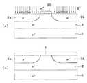
n型炭化珪素エピ層2の所定領域に、p型不純物をイオン注入する。その後、注入された不純物を活性化するために、高周波加熱炉内で熱処理を施す。この高周波加熱炉での熱処理の様子を図2に示して説明する。
【0033】
図2に示すように、高周波加熱炉100は、デバイスを形成するウェハ(この場合には、n-型炭化珪素エピ層2が形成されたn+型炭化珪素半導体基板1)200が搭載される試料台101を内蔵した加熱炉102と、この加熱炉102の外周に巻回された加熱用のコイル103とを備えて構成されている。加熱炉102は、ガス供給が行えるようになっており、炉内のガス雰囲気を設定できるようになっている。
【0034】
このように構成された高周波加熱炉100を用いて、ウェハ200を試料台101に搭載し、コイル103へ通電することで炉内を1300〜1700℃の温度にし、不純物の活性化のための熱処理(活性化アニール)を行う。このとき、ガス供給によって炉内をSiC雰囲気、例えば珪素水素化合物ガス及び炭化水素化合物ガスの混合雰囲気にすると共に、雰囲気の圧力を炭化珪素(SiC)が昇華する圧力(以下、昇華圧という)と同等にして熱処理を行う。
【0035】
また、このとき、珪素水素化合物ガスの分圧の方が炭化水素化合物ガスの分圧よりも高くなるようにしている。これは、熱処理の際に炭素が残ってしまうためであり、珪素の供給量を多くすることにより珪素供給不足をなくしている。
これにより、注入されたp型不純物が活性化され、p-型炭化珪素ベース領域3a、3bが形成される。
【0036】
このとき、雰囲気の圧力を炭化珪素の昇華圧と同等にして熱処理を行っているため、ウェハ表面(ここではn-型炭化珪素エピ層2の表面)の炭化珪素が昇華(気化)して消失する量と、ウェハ表面に炭化珪素が昇華(固化)して供給される量とが同等になり、ウェハ表面の炭化珪素が昇華(気化)して消失してしまうだけでなく、結晶化してウェハ表面に昇華(固化)して供給されるようになっているため、活性化のための熱処理によってウェハ表面に大きな凹凸が形成されないようにすることができる。
【0037】
このような条件で熱処理を行った場合、ウェハ表面には、平均2nm程度の凹凸しか形成されなかった。参考として、炭化珪素雰囲気でない条件下で熱処理を行ったところ、ウェハ表面に7nm程度の凹凸が形成された。
この結果から明らかなように、炭化珪素が気化する圧力と結晶化する圧力とがほぼ同等となる炭化珪素雰囲気下で熱処理を行うことにより、表面チャネル層5が形成されるp-型炭化珪素ベース領域3a、3bの表面に大きな凹凸が形成されないようにすることができる。
【0038】
なお、本実施形態の方法を用いた場合でも平均2nm程度の凹凸が認められたが、この程度の凹凸は現在入手可能なウェハの表面に初めから存在しているものであるため、本実施形態の方法によれば、ウェハ表面に形成されている凹凸をほとんど大きくしないように活性化のための熱処理を行っているといえる。
〔図1(b)に示す工程〕
そして、1200〜1500℃程度の温度下でp-型炭化珪素ベース領域3a、3bの表面を含むウェハ表面に表面チャネル層5を、例えばCVD法によってエピタキシャル成長させる。このとき、ウェハ表面となるn-型炭化珪素エピ層2の表面には大きな凹凸が形成されていないため、結晶性が良好な表面チャネル層5が形成される。
【0039】
この後、図8、図9に示す工程を経てプレーナ型パワーMOSFETを完成させる。このようにして、本実施形態におけるプレーナ型パワーMOSFETが製造される。
次に、この縦型パワーMOSFETの作用(動作)を説明する。
本MOSFETはノーマリオフ型の蓄積モードで動作するものであって、ポリシリコンゲート電極に電圧を印加しない場合は、表面チャネル層5においてキャリアは、p-型炭化珪素ベース領域3a、3bと表面チャネル層5との間の静電ポテンシャルの差、及び表面チャネル層5とポリシリコンゲート電極8との間の仕事関数の差により生じた電位によって全域空乏化される。ポリシリコンゲート電極8に電圧を印加することにより、表面チャネル層5とポリシリコンゲート電極8との間の仕事関数の差と外部からの印加電圧の和により生じる電位差を変化させる。このことにより、チャネルの状態を制御することができる。
【0040】
つまり、ポリシリコンゲート電極8の仕事関数を第1の仕事関数とし、p-型炭化珪素ベース領域3a、3bの仕事関数を第2の仕事関数とし、表面チャネル層5の仕事関数を第3の仕事関数としたとき、第1〜第3の仕事関数の差を利用して、表面チャネル層5のn型のキャリアを空乏化する様に第1〜第3の仕事関数と表面チャネル層5の不純物濃度及び膜厚を設定することができる。
【0041】
また、オフ状態において、空乏領域は、p-型炭化珪素ベース領域3a、3b及びポリシリコンゲート電極8により作られた電界によって、表面チャネル層5内に形成される。この状態からポリシリコンゲート電極8に対して正のバイアスを供給すると、ゲート絶縁膜(SiO2)7と表面チャネル層5との間の界面においてn+型ソース領域4a、4bからn-型ドリフト領域2方向へ延びるチャネル領域が形成され、オン状態にスイッチングされる。このとき、電子は、n+型ソース領域4a、4bから表面チャネル層5を経由し表面チャネル層5からn-型炭化珪素エピ層2に流れる。そして、n-型炭化珪素エピ層2(ドリフト領域)に達すると、電子は、n+型炭化珪素半導体基板1(n+ドレイン)へ垂直に流れる。
【0042】
このようにゲート電極8に正の電圧を印加することにより、表面チャネル層5に蓄積型チャネルを誘起させ、ソース電極10とドレイン電極11との間にキャリアが流れる。
このとき、上述したように、本実施形態におけるプレーナ型パワーMOSFETは、従来におけるプレーナ型MOSFETに比して表面チャネル層5の結晶性が良好なものとなっている。このため、本実施形態においては、従来のものよりも表面チャネル層5のチャネル移動度を向上させることができ、高移動度のプレーナ型パワーMOSFETとすることができる。
【0043】
なお、本実施形態では、p-型炭化珪素ベース領域3a、3bを形成する場合にのみ、上記雰囲気下で熱処理を行い、ウェハ表面に大きな凹凸が形成されないようにしているが、n+型ソース層4a、4bを形成する場合等にも上記雰囲気下で熱処理を行うようにしてもよい。
すなわち、表面チャネル層5を形成した後に、n+型ソース量4a、4bを形成するための熱処理を行っているが、この場合においても表面チャネル層5の表面の凹凸を大きくしてしまい、キャリア移動度を低下させる可能性があると考えられるが、このようにn+型ソース領域4a、4bを形成するための熱処理もウェハ表面に大きな凹凸が形成されないようにすれば、より結晶性の優れた高品質な表面チャネル層5とすることができる。
【0044】
また、表面チャネル層5を形成する前に、n+型ソース層4a、4bをp-型炭化珪素ベース領域3a、3bと同様の雰囲気下での熱処理で形成しておき、その後表面チャネル層5を形成するようにしてもよい。このような場合にも、n+型ソース層4a、4bを形成するための熱処理によってウェハ表面に大きな凹凸が形成されないため、結晶性の優れた表面チャネル層5とすることができる。
【0045】
なお、従来の方法でデバイスを製造した場合と、p-型炭化珪素ベース領域3a、3bを上記雰囲気下で形成した場合と、p-型炭化珪素ベース領域3a、3b及びn+型ソース層4a、4bを上記雰囲気下で形成した場合について、FET動作特性(ドレイン電流Id−ドレイン・ソース間電圧Vds特性)を同一ゲート電圧下で調べてみた。その結果を図3に示す。なお、図中では、従来の方法を実線で示してあり、p-型炭化珪素ベース領域3a、3bのみ上記雰囲気下で形成した場合を一点鎖線で示してあり、p-型炭化珪素ベース領域3a、3b及びn+型炭化珪素ベース領域4a、4bを上記雰囲気下で形成した場合を二点鎖線で示してある。
【0046】
この結果より、従来のプレーナ型パワーMOSFETに対して、p-型炭化珪素ベース領域3a、3bを上記雰囲気下で形成した場合の方がドレイン電流Idが顕著に増大していることが判る。また、n+型ソース層4a、4bを上記雰囲気下で形成した場合にはさらにドレイン電流Idが顕著に増大していることが判る。従って、プレーナ型パワーMOSFETの高移動度化が図れているといえる。
【0047】
このように、イオン注入された不純物の活性化の熱処理を、炭化珪素の昇華圧力と同等の圧力となる炭化珪素雰囲気下で行うことにより、表面チャネル層5の結晶性を良好にすることができ、プレーナ型パワーMOSFETの高移動度化を図ることができる。
(第2実施形態)
本実施形態では、表面チャネル層5をエピタキシャル成長させるときの熱処理を、p-型炭化珪素ベース領域3a、3bの形成の際の不純物を活性化させる熱処理と兼用する場合について説明する。
【0048】
なお、本実施形態におけるプレーナ型パワーMOSFETの製造工程は、図7〜図9に示される従来の製造工程とほぼ同じであるため、異なる部分のみ説明し、同様の部分については説明を省略する。
まず、上記と同様に図7(a)に示す工程を行い、n-型炭化珪素エピ層2を形成する。
【0049】
次に、以下に示す工程を実施する。
〔図4(a)に示す工程〕
n-型炭化珪素エピ層2の所定領域に、ボロン(B+)等のp型不純物300をイオン注入する。
〔図4(b)に示す工程〕
エピタキシャル成長法によって、n-型炭化珪素エピ層2の表面(ウェハ全面)に表面チャネル層5を形成し、さらにこの時の熱処理でp型不純物300を活性化させる。エピタキシャル成長の条件は、一般に行われるエピタキシャル成長の温度よりも高温な1300〜1700℃で熱処理を行うと共に、SiH4、C3H8、H2をソースガスとする。これにより、表面チャネル層5が形成されると共に、p-型炭化珪素ベース領域3a、3bが活性化される。
【0050】
このエピタキシャル成長の熱処理によって、ウェハ表面の炭化珪素が昇華(気化)するが、同時に表面チャネル層5をエピタキシャル成長させているため、ウェハ表面の炭化珪素が昇華(気化)してしまうよりも速いスピードでウェハ表面に炭化珪素が成膜されて、表面チャネル層5が形成される。
つまり、ウェハ表面に大きな凹凸が形成されるのは、ウェハ表面の炭化珪素が昇華(気化)する量が、雰囲気中からウェハ表面に昇華(固化)して炭化珪素となる量よりも多いからなので、ウェハ表面の炭化珪素が昇華(気化)する量が、雰囲気中からウェハ表面に昇華(固化)して炭化珪素となる量よりも少なくなればウェハ表面に大きな凹凸が形成されないのである。
【0051】
このような条件で熱処理を行った場合、表面チャネル層5の表面は、平均2nm程度の凹凸しか形成されなかった。参考として、上記従来の条件下(図7(b)に示す工程参照)で熱処理を行ったところ、表面チャネル層5の表面に7nm程度の凹凸が形成された。
この結果から明らかなように、ウェハ表面の炭化珪素が昇華(気化)してしまうよりも速くウェハ表面に炭化珪素を成膜し、表面チャネル層5を形成するようにすれば、結晶性の良好な表面チャネル層5を形成することができる。
【0052】
また、このように、表面チャネル層5の形成するためのエピタキシャル成長の際の熱処理と、p-型炭化珪素ベース領域3a、3bを形成する不純物の活性化のための熱処理とを兼用させているため、熱処理を別々に行う場合に比して製造工程を簡略化することができる。
この後、図8、図9に示す工程を経て、プレーナ型パワーMOSFETを完成させる。
【0053】
このようにして完成した本実施形態におけるプレーナ型パワーMOSFETは、従来におけるプレーナ型MOSFETに比して表面チャネル層5の結晶性が良好なものとなっているめ、従来のものよりも表面チャネル層5のチャネル移動度を向上させることができ、高移動度のプレーナ型パワーMOSFETとすることができる。
【0054】
なお、本実施形態では、表面チャネル層5の形成するためのエピタキシャル成長の際の熱処理と、p-型炭化珪素ベース領域3a、3bを形成する不純物の活性化のための熱処理とを兼用させたが、これに加えてn-型ソース層3a、3bを形成する不純物の活性化のための熱処理を兼用させることもできる。
すなわち、表面チャネル層5を形成する前に、p-型炭化珪素ベース領域3a、3bを形成するためのp型不純物のイオン注入と、n-型ソース層4a、4bを形成するためのn型不純物のイオン注入とを行っておき、その後表面チャネル層5をエピタキシャル成長させる熱処理にて、注入された不純物の活性化を行うこともできる。
【0055】
このようにすることで、n-型ソース領域4a、4bを形成するための不純物の活性化の熱処理の際に、表面チャネル層5の表面に大きな凹凸が形成されないようにすることができると共に、n-型ソース領域4a、4bを形成するための不純物の活性化の熱処理を別途行う必要をなくすことができるため、製造工程の簡略化を図ることができる。
【0056】
(他の実施形態)
上記第1実施形態では、高周波加熱炉100の中を炭化珪素雰囲気にするために、炭化珪素を構成するためのガスを供給するようにしているが、以下に示す方法を採用することも可能である。
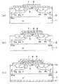
例えば、図5に示すように、高周波加熱炉100のうちデバイスを形成するウェハ(炭化珪素基板1)が搭載される試料台101に対抗する位置に試料台110を設けると共に、この試料台110にダミーの炭化珪素基板120を配置し、ダミーの炭化珪素基板120の炭化珪素を昇華(気化)させることによって、デバイスを形成するウェハ200の表面からあまり炭化珪素が昇華(気化)してしまわないようにするという方法を採用することができる。この場合において、ダミーの炭化珪素基板120を断面コの字をしたコップ形状とし、ウェハ200を全体的に覆うようにすれば、より効果を奏する。また、高周波加熱炉100内に予め炭化珪素粉末等を入れておき、この炭化珪素粉末を昇華(気化)させるようにする方法を採用することもできる。
【0057】
上記実施形態では、プレーナ型MOSFETを例に挙げて説明したが、チャネル層を基板表面に対して垂直とした、いわゆるトレンチ型(コンケーブ型)縦型MOSFETに本発明の一実施形態を適用してもよい。
なお、上記実施形態では、炭化珪素の結晶形を示す場合、所要の数字の上にバーを付した表現を取るべきであるが、表現手段に制約があるため、本明細書においては所要の数字の上にバーを付す代わりに、所要の数字の後ろに「−」を付して表現している。
【図面の簡単な説明】
【図1】第1実施形態におけるプレーナ型パワーMOSFETの製造工程を示す図である。
【図2】高周波加熱炉での熱処理を説明するための図である。
【図3】第1実施形態におけるプレーナ型パワーMOSFETの表面チャネル層5のキャリア移動度と、従来のものとを比較するための特性図である。
【図4】第2実施形態におけるプレーナ型パワーMOSFETの製造工程を示す図である。
【図5】他の実施形態における高周波加熱炉での熱処理を説明するための図である。
【図6】本出願人が先に出願した縦型パワーMOSFETの構成を示す断面図である。
【図7】図6に示す縦型パワーMOSFETの製造工程を示す図である。
【図8】図7に続く縦型パワーMOSFETの製造工程を示す図である。
【図9】図8に続く縦型パワーMOSFETの製造工程を示す図である。
【符号の説明】
1…n+型炭化珪素半導体基板、2…n-型炭化珪素エピタキシャル層、
3a、3b…p-型炭化珪素ベース領域、4a、4b…n+型ソース領域、
5…表面チャネル層(n-型SiC層)、7…ゲート絶縁膜、8…ゲート電極、
9…絶縁膜、10…ソース電極、11…ドレイン電極。[0001]
BACKGROUND OF THE INVENTION
The present invention relates to a method for manufacturing a silicon carbide semiconductor device, and more particularly to an insulated gate field effect transistor, particularly a vertical power MOSFET for high power.
[0002]
[Prior art]
The present applicant has filed in Japanese Patent Application No. 9-259076 for a vertical MOSFET with improved channel mobility and reduced on-resistance.
Among the vertical MOSFETs, a planar MOSFET is taken as an example, and a cross-sectional view thereof is shown in FIG. 6, and the structure of the planar vertical MOSFET will be described with reference to FIG.
[0003]
n+ Type silicon
At this time, n+ Type silicon
[0004]
n- P has a predetermined depth in a predetermined region in the surface layer portion of type
P- N region shallower than
[0005]
And n+
[0006]
This n- The
[0007]
The dopant concentration of the
P- Type silicon
[0008]
The upper surface of the
[0009]
Next, the manufacturing process of the planar power MOSFET shown in FIG. 6 will be described with reference to FIGS.
[Step shown in FIG. 7A]
First, an n-type 4H or 6H or 3C-SiC substrate, that is, n+ A silicon
[0010]
[Step shown in FIG. 7B]
n- After polishing the surface of the p-type
[0011]
[Step shown in FIG. 7C]
After the
[0012]
At this time, the thickness (film thickness) of the
[Step shown in FIG. 8 (a)]
An
[0013]
[Step shown in FIG. 8B]
Then, after removing the
[0014]
[Step shown in FIG. 8C]
Further, B is used with the
[0015]
The
[0016]
[Step shown in FIG. 9A]
After removing the
Thereafter, a
[0017]
[Step shown in FIG. 9B]
Subsequently, after unnecessary portions of the
[0018]
[Step shown in FIG. 9C]
Then, the
In this way, the vertical power MOSFET shown in FIG. 6 is completed.
[0019]
[Problems to be solved by the invention]
In the planar type MOSFET shown in FIG.- The type silicon
[0020]
By this heat treatment, p- Surface carbide layer (SiC) present on the surfaces of the type silicon
[0021]
The present invention has been made in view of the above points. In the case where the channel region is formed by epitaxial growth, the crystallinity of the channel region deteriorates due to the activation of the implanted impurity even when ion implantation is performed before epitaxial growth. It is an object of the present invention to provide a method for manufacturing a silicon carbide semiconductor device capable of preventing the above.
[0022]
[Means for Solving the Problems]
In order to achieve the above object, the following technical means are adopted.
In the first to eighth aspects of the invention, the second conductivity type impurity is ion-implanted into a predetermined region of the surface layer portion of the semiconductor layer (2), heat treatment is performed in a silicon carbide atmosphere, and the second conductivity type impurity is removed. A base region (3a, 3b) of the second conductivity type having a predetermined depth is formed by being activated.
[0023]
In this way, by performing heat treatment for activating the second conductivity type impurity ion-implanted to form the base region in a silicon carbide atmosphere, silicon carbide sublimates (vaporizes) and disappears from the surface of the semiconductor layer. In addition, since silicon carbide is supplied by sublimation (crystal growth) on the surface of the semiconductor layer, large unevenness can be prevented from being formed in the semiconductor layer. Since the surface channel layer (5) is formed on the surface of the semiconductor layer having such a good surface state, the surface channel layer can be made good without deteriorating the crystallinity.
[0024]
In the invention according to
Thus, even when forming the source region, the crystallinity of the surface channel layer can be made better by activating the impurities in a silicon carbide atmosphere.
[0025]
In addition, If the heat treatment for activating the second conductivity type impurity and the first conductivity type impurity is also used, the manufacturing process of the device can be simplified.
Claim3 In the invention described in (2), the silicon carbide atmosphere is characterized in that the pressure is substantially equal to the pressure at which silicon carbide sublimates.
[0026]
Thus, if the silicon carbide atmosphere is set to a pressure substantially equal to the pressure at which silicon carbide sublimates, the amount of silicon carbide sublimated (vaporized) from the surface of the semiconductor layer and the silicon carbide sublimated on the surface of the semiconductor layer ( Since the amount supplied by crystal growth) can be made equal, unevenness of the semiconductor layer can be prevented from becoming large even if heat treatment for activation is performed.
The silicon carbide atmosphere is claimed in
[0027]
[0028]
Thus, if the heat treatment for activating the second conductivity type impurity for forming the base region is performed by the heat treatment for epitaxial growth, the amount of silicon carbide sublimated (vaporized) and disappeared, Since the amount of silicon carbide supplied by sublimation (crystal growth) is larger, silicon carbide is deposited at a faster speed than the formation of irregularities on the surface of the semiconductor layer, thereby forming the surface channel layer. be able to. Thereby, the same effect as that of
[0029]
In order to combine the heat treatment for epitaxial growth with the heat treatment for impurity activation, the epitaxial growth is preferably performed at about 1300 to 1800 ° C., which is higher than the heat treatment for epitaxial growth that is generally performed.
[0030]
Thus, by activating the impurities by heat treatment during epitaxial growth and forming both the base region and the source region, the manufacturing process of the device can be further simplified, and the effect of
[0031]
DETAILED DESCRIPTION OF THE INVENTION
DESCRIPTION OF THE PREFERRED EMBODIMENTS Embodiments shown in the drawings will be described below.
(First embodiment)
The vertical power MOSFET shown in the present embodiment is different from the conventional manufacturing method and has the same structure as that of the vertical power MOSFET shown in FIG. 6, so only the manufacturing method will be described and the structure will be described. Is omitted. In this embodiment, since it is almost the same as the conventional manufacturing process shown in FIGS. 7 to 9, only different portions will be described, and description of similar portions will be omitted.
[0032]
First, similarly to the above, the process shown in FIG.- Type
Next, the following steps are performed.
[Step shown in FIG. 1 (a)]
A p-type impurity is ion-implanted into a predetermined region of n-type
[0033]
As shown in FIG. 2, the high-
[0034]
Using the high-
[0035]
At this time, the partial pressure of the silicon hydride gas is set higher than the partial pressure of the hydrocarbon compound gas. This is because carbon remains during the heat treatment, and an insufficient supply of silicon is eliminated by increasing the supply amount of silicon.
As a result, the implanted p-type impurity is activated, and p- Type silicon
[0036]
At this time, since the heat treatment is performed with the atmospheric pressure equal to the sublimation pressure of silicon carbide, the wafer surface (here n- The amount of silicon carbide on the surface of the silicon carbide epilayer 2) sublimated (vaporized) and disappeared is equivalent to the amount of silicon carbide sublimated (solidified) supplied to the wafer surface. Silicon is not only sublimated (vaporized) and disappears, but also crystallized and sublimated (solidified) to the surface of the wafer, so that large irregularities are formed on the wafer surface by heat treatment for activation. Can be prevented from being formed.
[0037]
When heat treatment was performed under such conditions, only irregularities with an average of about 2 nm were formed on the wafer surface. As a reference, when heat treatment was performed under conditions other than a silicon carbide atmosphere, irregularities of about 7 nm were formed on the wafer surface.
As is apparent from this result, the
[0038]
Even when the method of the present embodiment is used, irregularities of about 2 nm on average are recognized. However, since such irregularities are present on the surface of a wafer that is currently available, the present embodiment According to this method, it can be said that the heat treatment for activation is performed so that the unevenness formed on the wafer surface is hardly increased.
[Step shown in FIG. 1B]
And at a temperature of about 1200-1500 ° C., p-
[0039]
Thereafter, the planar type power MOSFET is completed through the steps shown in FIGS. In this way, the planar power MOSFET in the present embodiment is manufactured.
Next, the operation (operation) of this vertical power MOSFET will be described.
This MOSFET operates in a normally-off accumulation mode, and when no voltage is applied to the polysilicon gate electrode, carriers in the
[0040]
That is, the work function of the
[0041]
In the off state, the depletion region is p- Formed in
[0042]
Thus, by applying a positive voltage to the
At this time, as described above, the planar power MOSFET in the present embodiment has better crystallinity of the
[0043]
In this embodiment, p- Only when forming the type silicon
That is, after forming the
[0044]
Before forming the
[0045]
Note that when the device is manufactured by the conventional method, p.- Type silicon
[0046]
From this result, it can be seen that p.- It can be seen that the drain current Id is remarkably increased when the type silicon
[0047]
Thus, the crystallinity of the
(Second Embodiment)
In the present embodiment, the heat treatment when epitaxially growing the
[0048]
In addition, since the manufacturing process of the planar type power MOSFET in this embodiment is almost the same as the conventional manufacturing process shown in FIGS. 7 to 9, only different parts will be described and description of similar parts will be omitted.
First, similarly to the above, the process shown in FIG.- Type
[0049]
Next, the following steps are performed.
[Step shown in FIG. 4 (a)]
n- Boron (B+ ) And the like are ion-implanted.
[Step shown in FIG. 4B]
By epitaxial growth method, n-
[0050]
By this epitaxial growth heat treatment, silicon carbide on the wafer surface is sublimated (vaporized). However, since the
That is, large irregularities are formed on the wafer surface because the amount of silicon carbide on the wafer surface that sublimates (vaporizes) is larger than the amount that sublimates (solidifies) from the atmosphere to the wafer surface to form silicon carbide. If the amount of silicon carbide on the wafer surface that is sublimated (vaporized) is less than the amount of silicon carbide that is sublimated (solidified) from the atmosphere to the wafer surface, large irregularities are not formed on the wafer surface.
[0051]
When the heat treatment was performed under such conditions, the surface of the
As is apparent from this result, if the silicon carbide film is formed on the wafer surface faster than the silicon carbide on the wafer surface is sublimated (vaporized) to form the
[0052]
Further, in this way, heat treatment during epitaxial growth for forming the
Thereafter, the planar power MOSFET is completed through the steps shown in FIGS.
[0053]
The planar power MOSFET according to the present embodiment completed in this manner has better crystallinity of the
[0054]
In the present embodiment, heat treatment during epitaxial growth for forming the
That is, before forming the
[0055]
In this way, n- In the heat treatment for activating the impurities for forming the
[0056]
(Other embodiments)
In the first embodiment, a gas for constituting silicon carbide is supplied in order to make the silicon carbide atmosphere in the high-
For example, as shown in FIG. 5, a
[0057]
In the above embodiment, the planar MOSFET has been described as an example. However, the embodiment of the present invention is applied to a so-called trench type (concave type) vertical MOSFET in which the channel layer is perpendicular to the substrate surface. Also good.
In the above embodiment, when a silicon carbide crystal form is shown, it should be expressed with a bar on a required number. However, because there are restrictions on expression means, the required number is used in this specification. Instead of adding a bar above the symbol, “-” is appended to the required number.
[Brief description of the drawings]
FIG. 1 is a diagram illustrating a manufacturing process of a planar power MOSFET according to a first embodiment.
FIG. 2 is a view for explaining heat treatment in a high-frequency heating furnace.
FIG. 3 is a characteristic diagram for comparing the carrier mobility of the
FIG. 4 is a diagram showing a manufacturing process of a planar type power MOSFET in a second embodiment.
FIG. 5 is a view for explaining heat treatment in a high-frequency heating furnace according to another embodiment.
FIG. 6 is a cross-sectional view showing a configuration of a vertical power MOSFET previously filed by the present applicant.
7 is a diagram showing a manufacturing process of the vertical power MOSFET shown in FIG. 6. FIG.
8 is a diagram showing manufacturing steps of the vertical power MOSFET subsequent to FIG. 7. FIG.
FIG. 9 is a diagram illustrating manufacturing steps of the vertical power MOSFET subsequent to FIG. 8;
[Explanation of symbols]
1 ... n+ Type silicon carbide semiconductor substrate, 2... N- Type silicon carbide epitaxial layer,
3a, 3b ... p- Type silicon carbide base region, 4a, 4b... N+ Type source area,
5 ... surface channel layer (n- Type SiC layer), 7 ... gate insulating film, 8 ... gate electrode,
9 ... Insulating film, 10 ... Source electrode, 11 ... Drain electrode.
Claims (8)
Translated fromJapanese前記半導体層内の表層部の所定領域に、第2導電型不純物をイオン注入する工程と、
炭化珪素雰囲気下で熱処理を行い、前記第2導電型不純物を活性化させて所定深さを有する第2導電型のベース領域(3a、3b)を形成する工程と、
前記半導体層及び前記ベース領域の上部にチャネル領域となる表面チャネル層(5)をエピタキシャル成長させる工程と、
前記ベース領域内の表層部の所定領域に、前記表面チャネル層に接すると共に該ベース領域よりも浅い第1導電型のソース領域(4a、4b)を形成する工程と、
前記表面チャネル層の上部にゲート電極(8)を形成すると共に、前記ベース領域および前記ソース領域に接するソース電極(10)を形成する工程と、を含んでいることを特徴とする炭化珪素半導体装置の製造方法。Forming a first conductive type semiconductor layer (2) made of silicon carbide having a higher resistance than the semiconductor substrate on a main surface of the first conductive type semiconductor substrate (1) made of silicon carbide;
Ion-implanting a second conductivity type impurity into a predetermined region of the surface layerin the semiconductor layer;
Performing a heat treatment in a silicon carbide atmosphere to activate the second conductivity type impurities to form second conductivity type base regions (3a, 3b) having a predetermined depth;
Epitaxially growing a surface channel layer (5) to be a channel region on the semiconductor layer and the base region;
Forming a first conductivity type source region (4a, 4b) in contact with the surface channel layer and shallower than the base regionin a predetermined region of a surface layer portion in the base region;
Forming a gate electrode (8) above the surface channel layer, and forming a source electrode (10) in contact with the base regionand the source region. Manufacturing method.
前記半導体層内の表層部の所定領域に、第2導電型不純物をイオン注入する工程と、
エピタキシャル成長法により、前記半導体層の表面にチャネル領域となる表面チャネル層(5)をエピタキシャル成長させると共に、該エピタキシャル成長の熱処理によって前記第2導電型不純物を活性化させて第2導電型のベース領域(3a、3b)を形成する工程と、
前記ベース領域内の表層部の所定領域に、前記表面チャネル層に接すると共に該ベース領域よりも浅い第1導電型のソース領域(4a、4b)を形成する工程と、
前記表面チャネル層の上部にゲート電極(8)を形成すると共に、前記ベース領域に接するソース電極(10)を形成する工程と、を含んでいることを特徴とする炭化珪素半導体装置の製造方法。Forming a first conductive type semiconductor layer (2) made of silicon carbide having a higher resistance than the semiconductor substrate on a main surface of the first conductive type semiconductor substrate (1) made of silicon carbide;
Ion-implanting a second conductivity type impurity into a predetermined region of the surface layerin the semiconductor layer;
A surface channel layer (5) serving as a channel region is epitaxially grown on the surface of the semiconductor layer by an epitaxial growth method, and the second conductivity type impurities are activated by a heat treatment of the epitaxial growth to thereby form a second conductivity type base region (3a). 3b),
Forming a first conductivity type source region (4a, 4b) in contact with the surface channel layer and shallower than the base regionin a predetermined region of a surface layer portion in the base region;
Forming a gate electrode (8) above the surface channel layer and forming a source electrode (10) in contact with the base region. A method for manufacturing a silicon carbide semiconductor device, comprising:
前記半導体層内の表層部の所定領域に、第2導電型不純物をイオン注入する工程と、
前記半導体層内の表層部の所定領域に、第1導電型不純物をイオン注入する工程と、
エピタキシャル成長法により、前記半導体層の表面にチャネル領域となる表面チャネル層(5)をエピタキシャル成長させると共に、該エピタキシャル成長の熱処理によって前記第2導電型不純物を活性化させてベース領域(3a、3b)を形成し、さらに前記第1導電型不純物を活性化させて前記ベース領域の所定領域に、前記表面チャネル層に接すると共に前記ベース領域よりも浅いソース領域(4a、4b)を形成する工程と、
前記表面チャネル層の上部にゲート電極(8)を形成すると共に、前記ベース領域に接するソース電極(10)を形成する工程と、を含んでいることを特徴とする炭化珪素半導体装置の製造方法。Forming a first conductive type semiconductor layer (2) made of silicon carbide having a higher resistance than the semiconductor substrate on a main surface of the first conductive type semiconductor substrate (1) made of silicon carbide;
Ion-implanting a second conductivity type impurity into a predetermined region of the surface layerin the semiconductor layer;
Ion-implanting a first conductivity type impurity into a predetermined region of a surface layer portionin the semiconductor layer;
By epitaxial growth, a surface channel layer (5) serving as a channel region is epitaxially grown on the surface of the semiconductor layer, and the second conductivity type impurities are activated by heat treatment of the epitaxial growth to form base regions (3a, 3b). And activating the first conductivity type impurity to form a source region (4a, 4b) in contact with the surface channel layer and shallower than the base region in a predetermined region of the base region;
Forming a gate electrode (8) above the surface channel layer and forming a source electrode (10) in contact with the base region. A method for manufacturing a silicon carbide semiconductor device, comprising:
Priority Applications (1)
| Application Number | Priority Date | Filing Date | Title |
|---|---|---|---|
| JP07236598AJP3972450B2 (en) | 1998-03-20 | 1998-03-20 | Method for manufacturing silicon carbide semiconductor device |
Applications Claiming Priority (1)
| Application Number | Priority Date | Filing Date | Title |
|---|---|---|---|
| JP07236598AJP3972450B2 (en) | 1998-03-20 | 1998-03-20 | Method for manufacturing silicon carbide semiconductor device |
Publications (2)
| Publication Number | Publication Date |
|---|---|
| JPH11274481A JPH11274481A (en) | 1999-10-08 |
| JP3972450B2true JP3972450B2 (en) | 2007-09-05 |
Family
ID=13487224
Family Applications (1)
| Application Number | Title | Priority Date | Filing Date |
|---|---|---|---|
| JP07236598AExpired - Fee RelatedJP3972450B2 (en) | 1998-03-20 | 1998-03-20 | Method for manufacturing silicon carbide semiconductor device |
Country Status (1)
| Country | Link |
|---|---|
| JP (1) | JP3972450B2 (en) |
Families Citing this family (13)
| Publication number | Priority date | Publication date | Assignee | Title |
|---|---|---|---|---|
| JP3956487B2 (en)* | 1998-06-22 | 2007-08-08 | 富士電機デバイステクノロジー株式会社 | Method for manufacturing silicon carbide semiconductor device |
| JP4765175B2 (en)* | 2001-02-16 | 2011-09-07 | 株式会社デンソー | Method for manufacturing silicon carbide semiconductor device |
| JP4595224B2 (en)* | 2001-03-27 | 2010-12-08 | 株式会社デンソー | Method for manufacturing silicon carbide semiconductor device |
| JP2003068669A (en)* | 2001-08-27 | 2003-03-07 | Denso Corp | Method and device for heat treatment to semiconductor wafer |
| JP4639563B2 (en)* | 2001-09-17 | 2011-02-23 | 株式会社デンソー | Silicon carbide semiconductor manufacturing equipment |
| JP2005197464A (en) | 2004-01-07 | 2005-07-21 | Rohm Co Ltd | Manufacturing method of semiconductor device |
| JP2007335650A (en)* | 2006-06-15 | 2007-12-27 | Mitsubishi Electric Corp | Method for heating silicon carbide semiconductor substrate |
| JP2007335649A (en)* | 2006-06-15 | 2007-12-27 | Mitsubishi Electric Corp | Method for heating silicon carbide semiconductor substrate |
| JP2008034464A (en)* | 2006-07-26 | 2008-02-14 | New Japan Radio Co Ltd | Method for manufacturing semiconductor device |
| JP2008135611A (en)* | 2006-11-29 | 2008-06-12 | Denso Corp | Manufacturing method of semiconductor device |
| TW200931537A (en)* | 2007-12-11 | 2009-07-16 | Centrotherm Thermal Solutions Gmbh & Co Kg | Method and arrangement for tempering SiC wafers |
| JP5141227B2 (en)* | 2007-12-12 | 2013-02-13 | 住友電気工業株式会社 | Manufacturing method of semiconductor device |
| JP6271356B2 (en) | 2014-07-07 | 2018-01-31 | 株式会社東芝 | Manufacturing method of semiconductor device |
- 1998
- 1998-03-20JPJP07236598Apatent/JP3972450B2/ennot_activeExpired - Fee Related
Also Published As
| Publication number | Publication date |
|---|---|
| JPH11274481A (en) | 1999-10-08 |
Similar Documents
| Publication | Publication Date | Title |
|---|---|---|
| EP1981076B1 (en) | Method for manufacturing silicon carbide semiconductor device | |
| JP3893725B2 (en) | Method for manufacturing silicon carbide semiconductor device | |
| JP3385938B2 (en) | Silicon carbide semiconductor device and method of manufacturing the same | |
| EP2033212B1 (en) | Method of forming a silicon carbide pmos device | |
| US6117735A (en) | Silicon carbide vertical FET and method for manufacturing the same | |
| JP3760688B2 (en) | Method for manufacturing silicon carbide semiconductor device | |
| US8697555B2 (en) | Method of producing semiconductor device and semiconductor device | |
| JP4463448B2 (en) | SiC substrate and method of manufacturing SiC semiconductor device | |
| US8564017B2 (en) | Silicon carbide semiconductor device and method for manufacturing same | |
| US20120056202A1 (en) | Semiconductor device | |
| JP2000106371A (en) | Method for manufacturing silicon carbide semiconductor device | |
| JPH11238742A (en) | Method for manufacturing silicon carbide semiconductor device | |
| KR20060125700A (en) | Silicon Carbide Semiconductor Devices and Manufacturing Method Thereof | |
| JPWO2008056698A1 (en) | Silicon carbide semiconductor device and manufacturing method thereof | |
| JP3972450B2 (en) | Method for manufacturing silicon carbide semiconductor device | |
| JP4961633B2 (en) | Method for manufacturing silicon carbide semiconductor device | |
| JP4806852B2 (en) | Silicon carbide semiconductor device and manufacturing method thereof | |
| EP2139031A1 (en) | Semiconductor device and method for manufacturing semiconductor device | |
| JP2010034481A (en) | Method of manufacturing semiconductor device, and semiconductor device | |
| JP3944970B2 (en) | Method for manufacturing silicon carbide semiconductor device | |
| US20130171778A1 (en) | Method for manufacturing silicon carbide semiconductor device | |
| JP3941641B2 (en) | Silicon carbide semiconductor device manufacturing method and silicon carbide semiconductor device manufactured by the manufacturing method | |
| JP4042336B2 (en) | Silicon carbide semiconductor element | |
| JPH11121744A (en) | Semiconductor device and manufacture thereof | |
| JP4595224B2 (en) | Method for manufacturing silicon carbide semiconductor device |
Legal Events
| Date | Code | Title | Description |
|---|---|---|---|
| A621 | Written request for application examination | Free format text:JAPANESE INTERMEDIATE CODE: A621 Effective date:20040712 | |
| A977 | Report on retrieval | Free format text:JAPANESE INTERMEDIATE CODE: A971007 Effective date:20061222 | |
| A131 | Notification of reasons for refusal | Free format text:JAPANESE INTERMEDIATE CODE: A131 Effective date:20070306 | |
| A521 | Written amendment | Free format text:JAPANESE INTERMEDIATE CODE: A523 Effective date:20070424 | |
| TRDD | Decision of grant or rejection written | ||
| A01 | Written decision to grant a patent or to grant a registration (utility model) | Free format text:JAPANESE INTERMEDIATE CODE: A01 Effective date:20070522 | |
| A61 | First payment of annual fees (during grant procedure) | Free format text:JAPANESE INTERMEDIATE CODE: A61 Effective date:20070604 | |
| R150 | Certificate of patent or registration of utility model | Free format text:JAPANESE INTERMEDIATE CODE: R150 | |
| FPAY | Renewal fee payment (event date is renewal date of database) | Free format text:PAYMENT UNTIL: 20100622 Year of fee payment:3 | |
| FPAY | Renewal fee payment (event date is renewal date of database) | Free format text:PAYMENT UNTIL: 20100622 Year of fee payment:3 | |
| FPAY | Renewal fee payment (event date is renewal date of database) | Free format text:PAYMENT UNTIL: 20110622 Year of fee payment:4 | |
| FPAY | Renewal fee payment (event date is renewal date of database) | Free format text:PAYMENT UNTIL: 20110622 Year of fee payment:4 | |
| FPAY | Renewal fee payment (event date is renewal date of database) | Free format text:PAYMENT UNTIL: 20120622 Year of fee payment:5 | |
| FPAY | Renewal fee payment (event date is renewal date of database) | Free format text:PAYMENT UNTIL: 20120622 Year of fee payment:5 | |
| FPAY | Renewal fee payment (event date is renewal date of database) | Free format text:PAYMENT UNTIL: 20130622 Year of fee payment:6 | |
| LAPS | Cancellation because of no payment of annual fees |