JP3972066B2 - Light control type optical path switching type data distribution apparatus and distribution method - Google Patents
Light control type optical path switching type data distribution apparatus and distribution methodDownload PDFInfo
- Publication number
- JP3972066B2 JP3972066B2JP2004074874AJP2004074874AJP3972066B2JP 3972066 B2JP3972066 B2JP 3972066B2JP 2004074874 AJP2004074874 AJP 2004074874AJP 2004074874 AJP2004074874 AJP 2004074874AJP 3972066 B2JP3972066 B2JP 3972066B2
- Authority
- JP
- Japan
- Prior art keywords
- light
- optical
- signal
- control
- signal light
- Prior art date
- Legal status (The legal status is an assumption and is not a legal conclusion. Google has not performed a legal analysis and makes no representation as to the accuracy of the status listed.)
- Expired - Lifetime
Links
Images


Classifications
- G—PHYSICS
- G02—OPTICS
- G02F—OPTICAL DEVICES OR ARRANGEMENTS FOR THE CONTROL OF LIGHT BY MODIFICATION OF THE OPTICAL PROPERTIES OF THE MEDIA OF THE ELEMENTS INVOLVED THEREIN; NON-LINEAR OPTICS; FREQUENCY-CHANGING OF LIGHT; OPTICAL LOGIC ELEMENTS; OPTICAL ANALOGUE/DIGITAL CONVERTERS
- G02F1/00—Devices or arrangements for the control of the intensity, colour, phase, polarisation or direction of light arriving from an independent light source, e.g. switching, gating or modulating; Non-linear optics
- G02F1/29—Devices or arrangements for the control of the intensity, colour, phase, polarisation or direction of light arriving from an independent light source, e.g. switching, gating or modulating; Non-linear optics for the control of the position or the direction of light beams, i.e. deflection
- H—ELECTRICITY
- H04—ELECTRIC COMMUNICATION TECHNIQUE
- H04Q—SELECTING
- H04Q11/00—Selecting arrangements for multiplex systems
- H04Q11/0001—Selecting arrangements for multiplex systems using optical switching
- H04Q11/0005—Switch and router aspects
- G—PHYSICS
- G02—OPTICS
- G02F—OPTICAL DEVICES OR ARRANGEMENTS FOR THE CONTROL OF LIGHT BY MODIFICATION OF THE OPTICAL PROPERTIES OF THE MEDIA OF THE ELEMENTS INVOLVED THEREIN; NON-LINEAR OPTICS; FREQUENCY-CHANGING OF LIGHT; OPTICAL LOGIC ELEMENTS; OPTICAL ANALOGUE/DIGITAL CONVERTERS
- G02F1/00—Devices or arrangements for the control of the intensity, colour, phase, polarisation or direction of light arriving from an independent light source, e.g. switching, gating or modulating; Non-linear optics
- G02F1/29—Devices or arrangements for the control of the intensity, colour, phase, polarisation or direction of light arriving from an independent light source, e.g. switching, gating or modulating; Non-linear optics for the control of the position or the direction of light beams, i.e. deflection
- G02F1/31—Digital deflection, i.e. optical switching
- G—PHYSICS
- G02—OPTICS
- G02F—OPTICAL DEVICES OR ARRANGEMENTS FOR THE CONTROL OF LIGHT BY MODIFICATION OF THE OPTICAL PROPERTIES OF THE MEDIA OF THE ELEMENTS INVOLVED THEREIN; NON-LINEAR OPTICS; FREQUENCY-CHANGING OF LIGHT; OPTICAL LOGIC ELEMENTS; OPTICAL ANALOGUE/DIGITAL CONVERTERS
- G02F1/00—Devices or arrangements for the control of the intensity, colour, phase, polarisation or direction of light arriving from an independent light source, e.g. switching, gating or modulating; Non-linear optics
- G02F1/29—Devices or arrangements for the control of the intensity, colour, phase, polarisation or direction of light arriving from an independent light source, e.g. switching, gating or modulating; Non-linear optics for the control of the position or the direction of light beams, i.e. deflection
- G02F1/33—Acousto-optical deflection devices
- H—ELECTRICITY
- H04—ELECTRIC COMMUNICATION TECHNIQUE
- H04Q—SELECTING
- H04Q11/00—Selecting arrangements for multiplex systems
- G—PHYSICS
- G02—OPTICS
- G02F—OPTICAL DEVICES OR ARRANGEMENTS FOR THE CONTROL OF LIGHT BY MODIFICATION OF THE OPTICAL PROPERTIES OF THE MEDIA OF THE ELEMENTS INVOLVED THEREIN; NON-LINEAR OPTICS; FREQUENCY-CHANGING OF LIGHT; OPTICAL LOGIC ELEMENTS; OPTICAL ANALOGUE/DIGITAL CONVERTERS
- G02F1/00—Devices or arrangements for the control of the intensity, colour, phase, polarisation or direction of light arriving from an independent light source, e.g. switching, gating or modulating; Non-linear optics
- G02F1/01—Devices or arrangements for the control of the intensity, colour, phase, polarisation or direction of light arriving from an independent light source, e.g. switching, gating or modulating; Non-linear optics for the control of the intensity, phase, polarisation or colour
- G02F1/0147—Devices or arrangements for the control of the intensity, colour, phase, polarisation or direction of light arriving from an independent light source, e.g. switching, gating or modulating; Non-linear optics for the control of the intensity, phase, polarisation or colour based on thermo-optic effects
- G—PHYSICS
- G02—OPTICS
- G02F—OPTICAL DEVICES OR ARRANGEMENTS FOR THE CONTROL OF LIGHT BY MODIFICATION OF THE OPTICAL PROPERTIES OF THE MEDIA OF THE ELEMENTS INVOLVED THEREIN; NON-LINEAR OPTICS; FREQUENCY-CHANGING OF LIGHT; OPTICAL LOGIC ELEMENTS; OPTICAL ANALOGUE/DIGITAL CONVERTERS
- G02F1/00—Devices or arrangements for the control of the intensity, colour, phase, polarisation or direction of light arriving from an independent light source, e.g. switching, gating or modulating; Non-linear optics
- G02F1/29—Devices or arrangements for the control of the intensity, colour, phase, polarisation or direction of light arriving from an independent light source, e.g. switching, gating or modulating; Non-linear optics for the control of the position or the direction of light beams, i.e. deflection
- G02F1/293—Devices or arrangements for the control of the intensity, colour, phase, polarisation or direction of light arriving from an independent light source, e.g. switching, gating or modulating; Non-linear optics for the control of the position or the direction of light beams, i.e. deflection by another light beam, i.e. opto-optical deflection
- H—ELECTRICITY
- H04—ELECTRIC COMMUNICATION TECHNIQUE
- H04Q—SELECTING
- H04Q11/00—Selecting arrangements for multiplex systems
- H04Q11/0001—Selecting arrangements for multiplex systems using optical switching
- H04Q11/0005—Switch and router aspects
- H04Q2011/0007—Construction
- H04Q2011/0024—Construction using space switching
- H—ELECTRICITY
- H04—ELECTRIC COMMUNICATION TECHNIQUE
- H04Q—SELECTING
- H04Q11/00—Selecting arrangements for multiplex systems
- H04Q11/0001—Selecting arrangements for multiplex systems using optical switching
- H04Q11/0005—Switch and router aspects
- H04Q2011/0007—Construction
- H04Q2011/0026—Construction using free space propagation (e.g. lenses, mirrors)
- H—ELECTRICITY
- H04—ELECTRIC COMMUNICATION TECHNIQUE
- H04Q—SELECTING
- H04Q11/00—Selecting arrangements for multiplex systems
- H04Q11/0001—Selecting arrangements for multiplex systems using optical switching
- H04Q11/0005—Switch and router aspects
- H04Q2011/0037—Operation
- H04Q2011/0041—Optical control
Landscapes
- Physics & Mathematics (AREA)
- Nonlinear Science (AREA)
- Engineering & Computer Science (AREA)
- Computer Networks & Wireless Communication (AREA)
- General Physics & Mathematics (AREA)
- Optics & Photonics (AREA)
- Optical Modulation, Optical Deflection, Nonlinear Optics, Optical Demodulation, Optical Logic Elements (AREA)
- Optical Communication System (AREA)
Description
Translated fromJapanese本発明は光制御式光路切替型データ配信装置および配信方法に関する。更に詳しくは、企業のオフィス、工場、病院、一般家庭などにおいて、高精細画像データおよび高精細動画データなどの大容量デジタルデータを、サーバーから複数のクライアントの特定の1箇所へ、高速に配信するための光パケット通信方式の光制御式光路切替型データ配信装置および配信方法に関する。 The present invention relates to a light control type optical path switching type data distribution apparatus and distribution method. More specifically, large-capacity digital data such as high-definition image data and high-definition video data is distributed at high speed from a server to a specific location in a plurality of clients in a corporate office, factory, hospital, general household, etc. The present invention relates to an optically controlled optical path switching type data distribution apparatus and distribution method for optical packet communication.
パーソナルコンピューターおよびその周辺機器の著しい進歩の結果、高精細静止画像や動画画像などをデジタル化して記録した大容量デジタルデータを取り扱うことが日常化している。例えば、従来のカラーテレビジョン放送を一般家庭において、デジタル化してパーソナルコンピューターのハードディスク型記憶装置やDVDなどの光記録媒体に記録した場合、放映時間1時間当たり数GBもの大容量デジタルデータを取り扱うことになる。また、診断用医療機器の高度化にともない画素数1600×1200を越える超高精細静止画像やデジタルハイビジョン画像が、例えばガンの早期発見のために用いられている。一例として、画素数1600×1200の人体断層画像を1000枚組み合わせてディスプレイ上に「3次元」表示することで、1mm未満の早期ガンの発見も可能ともいわれている。 As a result of remarkable progress in personal computers and peripheral devices, it has become commonplace to handle large-capacity digital data recorded by digitizing high-definition still images and moving image images. For example, when a conventional color television broadcast is digitized in an ordinary home and recorded on a hard disk type storage device of a personal computer or an optical recording medium such as a DVD, large-capacity digital data of several GB per hour is handled. become. In addition, with the advancement of diagnostic medical equipment, ultra-high-definition still images and digital high-definition images that have more than 1600 × 1200 pixels are used for early detection of cancer, for example. As an example, it is said that it is possible to detect early cancer of less than 1 mm by combining 1000 human body tomographic images having 1600 × 1200 pixels and displaying them on a display “3D”.
近年、ハードディスク型記憶装置の容量が増大したため、このような高精細静止画像および動画の記録に関しては特に問題はない。しかしながら、離れた場所(病院内の別の部屋、大学病院の教室;遠隔治療のための別の場所)へ迅速に画像データを転送・送信するには「1Gbps」の高速LANを用いても数分ないし数十分の時間を要する。そこで、大容量デジタルデータを一旦、DVDなどの光記録媒体に記録して移動させることも行われているが、その場合には、記録および記録媒体の運搬に多大の時間を要することになる。また、医療用途では「電磁波障害対策」も必須であり、高速デジタルデータの送受信および伝送路切替に伴う電磁波の発生を極小化し、更に、外部からの電磁波からの干渉を受けなくするため、充分に電磁波シールドが施された送信側装置から光信号に変換された大容量デジタルデータを、途中で電気信号を一切用いず、光信号のまま、充分に電磁波シールドが施された受信側装置へ配信することが望まれる。 In recent years, since the capacity of hard disk storage devices has increased, there is no particular problem with recording such high-definition still images and moving images. However, even if a high-speed LAN of “1 Gbps” is used to quickly transfer and transmit image data to another place (another room in a hospital, a classroom in a university hospital; another place for telemedicine) It takes minutes or tens of minutes. Thus, large-capacity digital data is once recorded on an optical recording medium such as a DVD and moved. However, in that case, it takes a long time to record and transport the recording medium. In addition, "electromagnetic wave interference countermeasures" are also essential for medical applications, which minimizes the generation of electromagnetic waves associated with high-speed digital data transmission / reception and transmission path switching, and also prevents interference from external electromagnetic waves. Distributes large-capacity digital data converted from the transmitting device with the electromagnetic shielding to the optical signal to the receiving device with sufficient electromagnetic shielding without using any electrical signal on the way. It is desirable.
現在、データ通信速度10ないし40Gbps程度の「光トランシーバー」が大量生産されつつあるため、光ファイバーを活用したデータ配信装置の送信側と受信側についても技術的な課題は少ない。現在、光信号を用いるデータ配信分野において、最も開発が望まれている技術課題として、データ配信装置(サーバー)から複数のクライアント装置の特定の1箇所以上を選択して高速に配信するための、電気信号を経由しない光路切替装置(光スイッチ)、すなわち、光−光直接スイッチが求められている。 At present, since “optical transceivers” with a data communication speed of about 10 to 40 Gbps are being mass-produced, there are few technical problems on the transmitting side and the receiving side of the data distribution apparatus using optical fibers. Currently, in the field of data distribution using optical signals, as a technical issue that is most desired to be developed, for selecting one or more specific locations of a plurality of client devices from a data distribution device (server) for high-speed distribution, There is a need for an optical path switching device (optical switch) that does not pass through an electrical signal, that is, an optical-optical direct switch.
光ファイバー、光導波路、あるいは、空間を伝搬する光の進む道筋、すなわち、光路を切り替える装置・方法としては、例えば、光導波路内または光導波路間で光路を切り替える空間分割型、多重化された複数の波長の光を波長に応じた光路へ分割して切り替える波長分割多重型、一定時間毎に時分割多重化された光の光路を切り替える時分割多重型、空間を伝搬する光の光路を鏡やシャッターなどを用いて空間的に分割・合成するフリースペース型などの方式が知られている。これらの方式は、各々多重化することも複数を組み合わせて使用することもできる。 As an apparatus / method for switching an optical path, that is, an optical fiber, an optical waveguide, or a path of light propagating in space, for example, a space division type that switches an optical path in or between optical waveguides, and a plurality of multiplexed Wavelength-division multiplexing type that switches light of wavelength by dividing it into optical paths according to wavelength, time-division multiplexing type that switches the optical path of light that is time-division multiplexed every certain time, mirror or shutter for the optical path of light propagating in space There are known methods such as a free space type that spatially divides and synthesizes. Each of these methods can be multiplexed or used in combination.
空間分割型光スイッチには、方向性結合器を利用するもの、光分岐器で光信号のコピーを作り、ゲート素子により光をオン・オフするもの、交差またはY分岐の交差部分で導波路の屈折率を変化させることで、導波路を伝搬してきた光を透過させたり反射させたりするものなどが提案されているが、まだ研究開発段階である。マッハツェンダー干渉計型光導波路スイッチの導波路の屈折率を変化させるために、電気ヒーター加熱による熱光学効果を用いるものが実用化に近づいているといわれているが、応答速度が1ミリ秒程度と遅いだけでなく、光スイッチを動作させるために電気信号を用いなければならない、という欠点を有する。 The space division type optical switch uses a directional coupler, makes a copy of an optical signal with an optical branching device, turns on and off the light with a gate element, and guides the waveguide at the intersection of the intersection or Y branch. Proposals have been made to transmit or reflect light propagating through a waveguide by changing the refractive index, but it is still in the research and development stage. In order to change the refractive index of the waveguide of the Mach-Zehnder interferometer type optical waveguide switch, it is said that the one using the thermo-optic effect by heating the electric heater is approaching practical use, but the response speed is about 1 millisecond. Not only is it slow, it has the disadvantage that an electrical signal must be used to operate the optical switch.
フリースペース型光スイッチには、マイクロ・エレクトロ・メカニカル・システム(Micro Electro Mechanical System;MEMSと略記される。)、励起子吸収・反射スイッチ(Exciton Absorption Reflection Switch;EARSスイッチと略記される)、多段ビームシフタ型光スイッチ、ホログラム型光スイッチ、液晶スイッチなどが検討されている。これらは、機械的可動部分がある、偏波依存性があるなどの課題があり、まだ充分実用段階にあるとはいえない。 Free space type optical switches include Micro Electro Mechanical System (abbreviated as MEMS), Exciton Absorption Reflection Switch (abbreviated as EARS switch), multistage Beam shifter type optical switches, hologram type optical switches, liquid crystal switches, and the like have been studied. These have problems such as the presence of mechanically movable parts and polarization dependency, which are not yet in practical use.
一方、光学素子に光を照射することで引き起こされる透過率変化や屈折率変化を利用し、直接、光で光の強度や周波数を変調する、全光型光学素子や光制御方式の研究が盛んに行われている。本発明者らは、全光型光素子等による新たな情報処理技術の開発を目指して、有機色素凝集体をポリマーマトリックスに分散した有機ナノパーティクル光熱レンズ形成素子(非特許文献1参照)を用いて、光制御方式の研究を行って来た。現在、制御光(633nm)により信号光(780nm)の変調を行う方式で、制御光と信号光を同軸・同焦点入射させることを特徴とし、制御光の吸収により過渡的に形成される熱レンズにより信号光が屈折されるという動作原理の素子を開発しており、約20ナノ秒の高速応答が達成されている。光応答性組成物からなる光学素子に制御光を照射し、制御光とは異なる波長帯域にある信号光の透過率および/または屈折率を可逆的に変化させることにより前記光学素子を透過する前記信号光の強度変調および/または光束密度変調を行う光制御方法であって、前記制御光および前記信号光を各々収束させて前記光学素子へ照射し、かつ、前記制御光および前記信号光のそれぞれの焦点の近傍(ビームウエスト)の光子密度が最も高い領域が前記光学素子中において互いに重なり合うように前記制御光および前記信号光の光路を調整することを特徴とする光制御方法が開示されている(特許文献1から特許文献7参照)。光応答性組成物からなる光学素子に、互いに波長の異なる制御光および信号光を照射し、前記制御光の波長は前記光応答性組成物が吸収する波長帯域から選ばれるものとし、前記光応答性組成物が前記制御光を吸収した領域およびその周辺領域に発生する温度上昇に起因する密度変化の分布に基づいた熱レンズを可逆的に形成させ、前記熱レンズを透過する信号光の強度変調および/または光束密度変調を行う光制御方法が開示されている(特許文献8参照)。そして、上記光学素子として例えば色素/樹脂膜や色素溶液膜が用いられ、制御光のパワー2ないし25mWにおける制御光照射に対する信号光の応答時間は、2マイクロ秒未満と記載されている(特許文献8参照)。 On the other hand, research on all-optical optical elements and light control methods that directly modulate the intensity and frequency of light with light using changes in transmittance and refractive index caused by irradiating the optical element with light is actively conducted. Has been done. The present inventors have used an organic nanoparticle photothermal lens forming element (see Non-Patent Document 1) in which an organic dye aggregate is dispersed in a polymer matrix with the aim of developing a new information processing technique using an all-optical type optical element. I have studied light control systems. Currently, the control light (633 nm) is used to modulate the signal light (780 nm), the control light and the signal light are coaxially and confocally incident, and a thermal lens formed transiently by absorption of the control light Has developed an element based on the principle of operation in which signal light is refracted, and has achieved a high-speed response of about 20 nanoseconds. The optical element composed of the photoresponsive composition is irradiated with control light, and the optical element is transmitted through the optical element by reversibly changing the transmittance and / or refractive index of signal light in a wavelength band different from that of the control light. An optical control method for performing intensity modulation of signal light and / or light beam density modulation, wherein the control light and the signal light are respectively converged and applied to the optical element, and each of the control light and the signal light A light control method is disclosed in which the optical paths of the control light and the signal light are adjusted so that regions having the highest photon density near the focal point (beam waist) overlap each other in the optical element. (See
ここで熱レンズ効果とは、光吸収の中心部分において光を吸収した分子などが光を熱に変換し、この熱が周囲に伝搬されることにより温度分布が生じ、その結果、光透過媒体の屈折率が光吸収中心から外部へ向けて球状に変化して光吸収中心の屈折率が低く外部へ向けて屈折率が高くなる分布を生じ、これが凹レンズのように機能するような光の屈折効果を示す。熱レンズ効果は分光分析の分野で古くから利用されており、現在では分子1個による光吸収をも検出するような超高感度分光分析も可能になっている(非特許文献2および非特許文献3参照)。 Here, the thermal lens effect means that molecules that absorb light in the central part of light absorption convert light into heat, and this heat is propagated to the surroundings, resulting in a temperature distribution. The refractive index of the light changes such that the refractive index changes spherically from the light absorption center to the outside, resulting in a distribution in which the refractive index at the light absorption center is low and the refractive index increases toward the outside, which functions like a concave lens. Indicates. The thermal lens effect has been used for a long time in the field of spectroscopic analysis, and now it is possible to perform ultrasensitive spectroscopic analysis that detects light absorption by a single molecule (Non-Patent
熱レンズ効果ないし熱による屈折率変化を用いて光路を偏向させる方式として、発熱抵抗体で媒体に熱を与え、媒体内に屈折率分布を生じさせ、光を偏向する方法が開示されている(特許文献9参照)。しかしながら、上述の手法は、発熱抵抗体で発熱させ、熱伝導で媒体を加熱することになるので、「熱の拡がり」という問題を本来的に有する。つまり、熱の拡がりにより、広い面積内で微細な熱勾配を与えることができず、所望の屈折率分布を得るのが困難である。更に、発熱抵抗体の微細加工は半導体集積回路で用いられているフォトリソグラフィ技術を採用しても、現実には一定の限界を有し、素子が大型化せざるを得ない。素子が大型化すれば、それにともない光学系も複雑かつ大型化する。また、発熱抵抗体で発熱させ、熱伝導で媒体を加熱することになるので、応答が遅く、屈折率変化の周波数を上げることができないという不具合を本質的な問題として有している。 As a method of deflecting an optical path by using a thermal lens effect or a refractive index change due to heat, a method of deflecting light by applying heat to a medium with a heating resistor to generate a refractive index distribution in the medium is disclosed ( (See Patent Document 9). However, the above-described method inherently has a problem of “spreading of heat” because heat is generated by the heating resistor and the medium is heated by heat conduction. That is, due to the spread of heat, a fine thermal gradient cannot be given within a wide area, and it is difficult to obtain a desired refractive index distribution. Furthermore, even if the photolithography technique used in the semiconductor integrated circuit is adopted for microfabrication of the heating resistor, there is a certain limit in practice, and the element must be enlarged. As the element becomes larger, the optical system becomes more complicated and larger. In addition, since the medium is heated by heat generation by generating heat with a heat generating resistor, the response is slow and the problem that the frequency of refractive index change cannot be increased is an essential problem.
また、光応答組成物からなる光学素子と、該光学素子にくさび形の光強度分布で光を照射するための強度分布調整手段とから少なくとも構成され、制御光により前記光学素子中に屈折率分布を形成し、該屈折率分布により前記制御光とは異なる波長の信号光の偏向を行うことを特徴とする光学素子を用いた偏向素子が開示されている(特許文献10参照)。この方式は、光で光を制御する点では優れたものであるが、偏向角度が30度以内という制約があり、光路切替方向を自由に設定することができないという問題がある。 And an optical element comprising a photoresponsive composition and an intensity distribution adjusting means for irradiating the optical element with light with a wedge-shaped light intensity distribution, and a refractive index distribution in the optical element by control light. And a deflection element using an optical element characterized in that the signal light having a wavelength different from that of the control light is deflected by the refractive index distribution (see Patent Document 10). This method is excellent in that the light is controlled by light, but there is a limitation that the deflection angle is within 30 degrees, and there is a problem that the optical path switching direction cannot be freely set.
そこで本発明者らは、偏波依存性のない、光路切替の角度および方向を自由に設定可能な、信号光の光強度減衰が少なく多重連結使用が可能な光路切替装置および光路切替方法を提供するため、少なくとも光吸収層膜を含む熱レンズ形成素子中の光吸収層膜に、前記光吸収層膜が吸収する波長帯域から選ばれる波長の制御光、および、前記光吸収層膜が吸収しない波長帯域から選ばれる波長の信号光を各々収束させて照射し、少なくとも前記制御光が前記光吸収層膜内において焦点を結ぶように配置を調整し、前記光吸収層膜が前記制御光を吸収した領域およびその周辺領域に起こる温度上昇に起因して可逆的に生ずる屈折率の分布に基づいた熱レンズを用いることによって、制御光が照射されず熱レンズが形成されない場合は前記収束された信号光が通常の開き角度で前記熱レンズ形成素子から出射する状態と、制御光が照射されて熱レンズが形成される場合は前記収束された信号光が通常の開き角度よりも大きい開き角度で前記熱レンズ形成素子から出射する状態とを、前記制御光の照射の有無に対応させて実現させ、制御光が照射されず熱レンズが形成されない場合は、通常の開き角度で前記熱レンズ形成素子から出射する前記信号光をそのまま、または、受光レンズによって前記通常の開き角度を変更させた後、前記信号光が通過する穴を設けた鏡の穴を通して直進させ、一方、制御光が照射されて熱レンズが形成される場合は、通常よりも大きい開き角度で前記熱レンズ形成素子から拡がりながら出射する前記信号光をそのまま、あるいは、受光レンズによって前記拡がりの開き角度を変更させた後、前記穴付ミラーを用いて反射することによって光路を変更させる光路切替装置および光路切替方法を出願した(特許文献11および12参照)。 Therefore, the present inventors provide an optical path switching apparatus and an optical path switching method that can freely set the angle and direction of optical path switching without polarization dependence, can reduce the light intensity of signal light, and can be used in multiple connection. Therefore, the light absorbing layer film in the thermal lens forming element including at least the light absorbing layer film does not absorb the control light having a wavelength selected from the wavelength band absorbed by the light absorbing layer film and the light absorbing layer film. The signal light having a wavelength selected from a wavelength band is converged and irradiated, and the arrangement is adjusted so that at least the control light is focused in the light absorption layer film, and the light absorption layer film absorbs the control light. By using a thermal lens based on a refractive index distribution that occurs reversibly due to a temperature rise occurring in the region and its surrounding region, the control lens is not irradiated and the thermal lens is not converged. When the signal light is emitted from the thermal lens forming element at a normal opening angle, and when the control light is irradiated to form a thermal lens, the converged signal light has an opening angle larger than the normal opening angle. When the thermal lens forming element is realized in correspondence with the presence or absence of irradiation of the control light, and the thermal lens is not formed without being irradiated with the control light, the thermal lens forming element is formed at a normal opening angle. The signal light emitted from the light beam is changed as it is or after the normal opening angle is changed by a light receiving lens, and then travels straight through a hole in a mirror provided with a hole through which the signal light passes, while the control light is irradiated. When a thermal lens is formed, the signal light emitted while spreading from the thermal lens forming element at an opening angle larger than usual is left as it is or is spread by the light receiving lens. After changing the opening angle of, it filed the optical path switching device and the optical path switching method for changing an optical path by reflecting using the mirror with the hole (see
本発明は、機械的可動部分を用いずに故障のない、高速で作動し、耐久性の高い、偏波依存性のない、電磁波障害を起こさず電磁波の影響を受けない、光パケット通信方式に係る光制御式光路切替型データ配信装置および配信方法を提供することを目的とする。 The present invention is an optical packet communication system that does not use mechanical moving parts, operates without failure, operates at high speed, has high durability, does not depend on polarization, does not cause electromagnetic interference, and is not affected by electromagnetic waves. It is an object of the present invention to provide a light control type optical path switching type data distribution apparatus and distribution method.
上記の目的を達成するため、本発明の光制御式光路切替型データ配信装置は、複数のクライアント装置の中から選択された1つ以上の特定のクライアント装置にデータサーバー装置からデータを提供するデータ配信装置であって、
少なくともデータサーバー装置、データ通信部、および、クライアント装置からなり、
前記データ通信部は、少なくとも、光スイッチ、光信号路、光信号送信部、光信号受信部、および、データ送受信制御部からなり、
前記光信号送信部は、少なくとも
1種類以上の波長の信号光を照射する信号光光源と、
前記データ送受信制御部からの制御信号に応じて、前記信号光とは異なる3種類以上の波長の制御光を照射する制御光光源とを有し、
前記光スイッチは、少なくとも
前記信号光は透過し、前記制御光の特定の1種類の波長のみを各々選択的に吸収する1つ以上の光吸収層膜と、
前記光吸収層膜の1つ1つに前記制御光と前記信号光とを各々収束させて照射する手段と、
前記光吸収層膜を含み、前記光吸収層膜が前記特定の1種類の波長の制御光を吸収した領域およびその周辺領域に起こる温度上昇に起因して可逆的に生ずる屈折率の分布に基づいた熱レンズを用いることによって、前記特定の1種類の波長の制御光の照射の有無に応じ、前記収束された信号光を収束させたまま出射する、信号光の開き角度を拡大させて出射する、または、通常の開き角で出射する1つ以上の熱レンズ形成素子と、
前記各熱レンズ形成素子の各々後方に設けられた、穴と反射手段とを有する鏡であって、前記特定の1種類の波長の制御光の照射の有無に応じて、前記熱レンズ形成素子を出射した信号光を前記穴に通過させ、または、前記反射手段により反射させることによって光路を変化させる鏡と、
を備えることを特徴とする。In order to achieve the above object, an optically controlled optical path switching type data distribution apparatus according to the present invention provides data that provides data from a data server apparatus to one or more specific client apparatuses selected from a plurality of client apparatuses. A distribution device,
At least a data server device, a data communication unit, and a client device,
The data communication unit comprises at least an optical switch, an optical signal path, an optical signal transmission unit, an optical signal reception unit, and a data transmission / reception control unit,
The optical signal transmitter includes a signal light source that emits signal light having at least one wavelength,
In accordance with a control signal from the data transmission / reception control unit, a control light source that emits control light havingthree or more types of wavelengths different from the signal light,
The optical switch transmits at least the signal light and selectively absorbs only one specific type of wavelength of the control light; and
Means for converging and irradiating the control light and the signal light to each of the light absorption layer films;
Based on a refractive index distribution that reversibly occurs due to a temperature rise that occurs in a region where the light absorbing layer film absorbs the control light of the specific one type of wavelength and its peripheral region. By using the thermal lens, the converged signal light is emitted while being converged according to the presence or absence of the control light of the specific one type of wavelength. Or one or more thermal lens forming elements that emit at a normal opening angle;
Each of the thermal lens forming elements is a mirror having a hole and a reflection means provided at the back of each of the thermal lens forming elements, wherein the thermal lens forming element is changed depending on whether or not the control light of the specific one type of wavelength is irradiated. A mirror that changes the optical path by allowing the emitted signal light to pass through the hole or reflected by the reflecting means;
It is characterized by providing.
また、本発明の他の光制御式光路切替型データ配信装置は、上記装置において、前記データ通信部は、少なくとも、任意の大きさのデジタル情報を固定長ないし可変長の光デジタル信号の集まりとしての光パケットに分割して前記信号光として照射・送信し、
前記光パケットの照射に同期させて、前記光パケット毎に送信先クライアント装置についての識別情報を表す光タグを前記制御光として照射して前記光スイッチを作動させることを特徴とする。According to another optical control type optical path switching type data distribution apparatus of the present invention, in the above apparatus, the data communication unit at least sets digital information of an arbitrary size as a collection of optical digital signals having a fixed length or a variable length. Divide into optical packets and irradiate and transmit as the signal light,
In synchronization with the irradiation of the optical packet, the optical switch is operated by irradiating an optical tag representing identification information about a destination client device for each optical packet as the control light.
上記の目的を達成するため、また、本発明の光制御式光路切替型データ配信方法は、光信号に変換されたデータを搬送する1種類以上の波長の信号光と、
データの搬送先に対応して制御光光源から照射される、前記信号光とは異なる3種類以上の波長の制御光とを、実質的に同軸かつ同方向に進行させ、
前記信号光は透過し、前記制御光の特定の1種類の波長のみを各々選択的に吸収する1つ以上の光吸収層膜の1つ1つに前記制御光と前記信号光とを各々収束させて照射し、
前記光吸収層膜を含む1つ以上の熱レンズ形成素子の個々において、前記光吸収層膜が前記特定の1種類の波長の制御光を吸収した領域およびその周辺領域に起こる温度上昇に起因して可逆的に生ずる屈折率の分布に基づいた熱レンズを用いることによって、前記特定の1種類の波長の制御光の照射の有無に応じ、前記収束された信号光を収束させたまま出射させ、信号光の開き角度を拡大させて出射させ、または、通常の開き角で出射させ、
反射面を有する穴付ミラーを用い、前記特定の1種類の波長の制御光の照射の有無に応じて、前記熱レンズ形成素子から出射した信号光を前記穴から通過直進させ、または、反射面で反射させることによって光路を変更させて、
複数のクライアント装置の中から選択された1つ以上の特定のクライアント装置にデータを配信することを特徴とする。
In order to achieve the above object, the optically controlled optical path switching type data distribution method of the present invention includes a signal light having one or more wavelengths carrying data converted into an optical signal,
The control light ofthree or more wavelengths different from the signal light emitted from the control light source corresponding to the data transport destination is substantially coaxial and travels in the same direction,
The control light and the signal light are converged on each of one or more light absorption layer films that transmit the signal light and selectively absorb only one specific wavelength of the control light, respectively. Let it irradiate,
In each of the one or more thermal lens forming elements including the light absorption layer film, the light absorption layer film is caused by a temperature rise that occurs in a region where the control light of the specific one type of wavelength is absorbed and its peripheral region. By using a thermal lens based on a refractive index distribution reversibly generated, the converged signal light is emitted while being converged according to the presence or absence of the control light of the specific one type of wavelength, Increase the opening angle of the signal light and emit it, or emit it with a normal opening angle,
Using a mirror with a hole having a reflective surface, the signal light emitted from the thermal lens forming element passes straight through the hole in accordance with the presence or absence of the control light having the specific one type of wavelength, or the reflective surface Change the optical path by reflecting the
Data is distributed to one or more specific client devices selected from a plurality of client devices.
また、本発明の他の光制御式光路切替型データ配信方法は、上記配信方法において、前記信号光は、任意の大きさのデジタル情報が固定長ないし可変長のデジタル信号の集まりとして分割されたパケットを光パケットとして搬送し、
前記制御光は、前記光パケット毎に送信先クライアント装置についての識別情報を表す光タグとして前記光パケットの照射に同期させて照射され、前記光パケットの光路を変更することを特徴とする。According to another optical control type optical path switching type data distribution method of the present invention, in the above distribution method, the signal light is divided as a collection of digital signals having a fixed length or a variable length. Carry packets as optical packets,
The control light is emitted as an optical tag representing identification information about a destination client device for each optical packet in synchronization with irradiation of the optical packet, and changes an optical path of the optical packet.
また、本発明の他の光制御式光路切替型データ配信装置は、上記装置において、複数のクライアント装置の中から選択された1つ以上の特定のクライアント装置にデータサーバー装置からデータとしてデジタル静止画像または動画像を配信することを特徴とする。 According to another aspect of the present invention, there is provided an optical control type optical path switching type data distribution apparatus, wherein, in the above apparatus, one or more specific client devices selected from a plurality of client devices are digital still images as data from the data server device. Alternatively, a moving image is distributed.
また、本発明の他の光制御式光路切替型データ配信装置は、上記装置において、複数のクライアント装置の中から選択された1つ以上の特定のクライアント装置にデータサーバー装置からデータとして医療用デジタル静止画像または動画像を配信することを特徴とする。 According to another optical control type optical path switching type data distribution apparatus of the present invention, in the above apparatus, one or more specific client devices selected from a plurality of client devices are used as medical digital data as data from the data server device. A still image or a moving image is distributed.
本発明によれば、機械的可動部分を用いずに故障のない、高速で作動し、耐久性の高い、偏波依存性のない、電磁波障害を起こさず電磁波の影響を受けない、光パケット通信方式に係る光制御式光路切替型データ配信装置および配信方法を提供することができる。 According to the present invention, optical packet communication that does not use a mechanical moving part, operates without failure, operates at high speed, has high durability, does not depend on polarization, does not cause electromagnetic interference, and is not affected by electromagnetic waves. It is possible to provide a light control type optical path switching type data distribution apparatus and distribution method according to the method.
[光パケット通信の原理]
電気通信の分野におけるパケット通信方式では、任意の大きさのデジタル情報(データ)を固定長ないし可変長のデジタル信号の集まりとしてのパケット(packet;小包)に分割し、パケット毎に送信先および再構成の順序についての識別情報を表すタグ(tag;荷札)を付加して送信し、通信経路上の通信経路制御装置はタグの識別情報に基づいて送信先を特定してパケットを送り届け、受信側ではタグの識別情報に基づいて、パケットに分割された細切れの情報の順位(順序)を揃えて再構成して元の情報を復元・受理している。[Principle of optical packet communication]
In packet communication systems in the field of telecommunications, digital information (data) of an arbitrary size is divided into packets (packets) as a collection of fixed-length or variable-length digital signals. A tag (tag) indicating identification information about the order of the configuration is added and transmitted, and the communication path control device on the communication path specifies the transmission destination based on the identification information of the tag and delivers the packet to the receiving side. Then, based on the identification information of the tag, the order (order) of pieces of information divided into packets is arranged and reconstructed to restore and accept the original information.
本発明の光制御式光路切替型データ配信装置および配信方法は、このような電気信号のパケットおよびタグを光に置き換えるものである。すなわち、任意の大きさのデジタル情報(データ)を固定長ないし可変長の光信号の集まりとしての光パケットに分割して信号光として送受信し、光パケット毎に送信先についての識別情報を表す「光宛先タグ」、および、再構成の順序についての識別情報を表す「光順位タグ」を付加して送信し、通信経路上の光制御式光スイッチは光宛先タグの識別情報に基づいて送信先を特定して光パケットを送り届けるために作用し、受信側では光順位タグの識別情報に基づいて光パケットに分割されて送信された細切れの情報を再構成して元のデジタル情報を得ようとするものである。ここで、光パケット毎に送信先を表す光宛先タグとしては、信号光とは波長の異なる制御光が用いられ、一方、光パケットの再構成の順序についての識別情報を表す光順位タグについては光パケットそのものに付加されて信号光として送信されるものとする。 The optically controlled optical path switching type data distribution apparatus and distribution method of the present invention replace such electric signal packets and tags with light. That is, digital information (data) of an arbitrary size is divided into optical packets as a collection of fixed-length or variable-length optical signals and transmitted / received as signal light, and identification information about the transmission destination is expressed for each optical packet. "Optical destination tag" and an "optical rank tag" indicating identification information about the order of reconstruction are added and transmitted. The optically controlled optical switch on the communication path transmits the transmission destination based on the identification information of the optical destination tag. The receiving side tries to obtain the original digital information by reconfiguring the pieces of information that are divided into optical packets and transmitted based on the identification information of the optical rank tag. To do. Here, as the optical destination tag representing the transmission destination for each optical packet, control light having a wavelength different from that of the signal light is used. On the other hand, for the optical rank tag representing the identification information about the reconfiguration order of the optical packet, It is assumed that it is added to the optical packet itself and transmitted as signal light.
例えば、図1および図2において、データサーバー装置1000からクライアント装置1201、1202、および、1203へ各々送信されるデータ12010、12020、および、12030などは、データ通信部1100において、データ送受信制御部1140によって、まず、電気信号パケットに分割され、個々の電気信号パケットには電気信号の順位タグが付加された後、光信号送信部1120にて光パケット12011、12021、12031、12012、12013などに変換されて送信され、光信号路1110を通じて光スイッチ1101において、各々の光パケットに同期して光信号送信部1120から照射される光宛先タグ12111、12121、12131、12112、12113などの作用によって光信号路1111、1112、および、1113に光路切替される。これらの光信号路の末端には各々、光信号受信部1131、1132、および、1133が設けられ、ここで受光された光パケットは電気信号パケットに変換され、データ送受信制御部1141、1142、および、1143において電気信号パケット中の順位タグに記録された再構成の順序についての識別情報に基づいて、元のデータ12010、12020、12030などに再構成され、各々、クライアント装置1201、1202、および、1203に電気信号として配信される。図2に示すように、例えば、元のデータ12010は、光パケットの情報部分12311、12312、および、12313に分割されて、光パケットとして光スイッチによって光路切替されて配信された後、光順位タグ12211、12212、および、12213として配信されたデータ再構成の順序についての識別情報に基づいて復元され、クライアント装置1201へ配信される。 For example, in FIGS. 1 and 2,
[光パケットと光宛先タグの同期]
光パケットと光宛先タグの同期は、例えば以下のようにして実施される。[Synchronization of optical packet and optical destination tag]
The synchronization between the optical packet and the optical destination tag is performed as follows, for example.
データ送信側のデータ送受信制御部1140が発生する基準クロックパルスは、例えば図3に示すように、ON状態13000、13002、13004、13006などとOFF状態13001、13003、13005などが交互に同一のパルス時間幅tp(例えば125ミリ秒)で並んでいるものとする。光パケット12000、12001などは基準クロックパルスのON状態とOFF状態の双方に対応して発信され、いずれの場合も、基準クロックパルスの立ち上がりおよび立ち下がりから、予め設定された遅延時間Δtに相当する時間だけ遅れて発信されるものとする。この遅延時間Δtは、実施例にて詳細に説明するように、本発明で用いられる光スイッチにおける光路切替に要する時間に応じて設定される(例えば、パルス時間幅tp125ミリ秒に対して、遅延時間Δt1ミリ秒)。一方、波長の異なる1つ以上の制御光光源から発信される波長(1)、(2)、(3)などの光宛先タグは、基準クロックパルスに同期して発信される。図3に示す例においては、例えば、基準クロックパルスON状態13002に対応して波長(1)の光宛先タグ12111と光パケット12011が、同OFF状態13003に対応して波長(2)の光宛先タグ12121と光パケット12021が、同ON状態13004に対応して波長(3)の光宛先タグ12131と光パケット12031が、それぞれ同期して発信される。また、例えば、光宛先タグ12112と12113が連続して照射・発信された場合は、対応する光パケット12012と12013は対応する同一クライアント装置(この場合、1201)へ連続して配信される。For example, as shown in FIG. 3, the reference clock pulse generated by the data transmission / reception control unit 1140 on the data transmission side is the same pulse alternately in the ON states 13000, 13002, 13004, 13006, and the OFF states 13001, 13003, 13005, etc. It is assumed that they are arranged with a time width tp (for example, 125 milliseconds).
[光制御式光路切替型データ配信装置を構成する要素]
本発明の光制御式光路切替型データ配信装置を構成する要素を図1に示す。以下、これらの要素について順を追って説明する。[Elements of a light control type optical path switching type data distribution apparatus]
The elements constituting the light control type optical path switching type data distribution apparatus of the present invention are shown in FIG. Hereinafter, these elements will be described in order.
[データサーバー装置]
データサーバー装置1000は、少なくともデータ収集部1050と送信データ記憶部1010を持ち、更に、通常のコンピューターと同様に入出力制御部1040、補助記憶部、外部記憶部、電源部などからなる。[Data server device]
The data server apparatus 1000 includes at least a data collection unit 1050 and a transmission data storage unit 1010, and further includes an input / output control unit 1040, an auxiliary storage unit, an external storage unit, a power supply unit, and the like as in a normal computer.
データ収集部1050は公知の任意のデータ入力装置からなり、必要に応じて一時記憶装置(バッファメモリ)などの補助記憶部を有しても良い。データ入力装置の具体例としては、例えば、RS−232C、IEEE1394、USB2.0、SCSIなどのデジタルデータ通信規格に準拠した入力インターフェース、フロッピー(登録商標)ディスクドライブ、CDドライブ、DVDドライブ、磁気テープ装置、各種半導体メモリー読み取り装置などの記録媒体読み取り装置、テレビジョン画像のデジタルインターフェースボードなどを挙げることができる。 The data collection unit 1050 includes any known data input device, and may include an auxiliary storage unit such as a temporary storage device (buffer memory) as necessary. Specific examples of the data input device include, for example, an input interface compliant with digital data communication standards such as RS-232C, IEEE 1394, USB 2.0, SCSI, floppy (registered trademark) disk drive, CD drive, DVD drive, and magnetic tape. Apparatus, recording medium reader such as various semiconductor memory readers, television image digital interface board, and the like.
送信データ記憶部1010は、公知の任意のデジタルデータ記憶・記録装置からなり、必要に応じて高速に動作する一時記憶装置(バッファメモリ)などの補助記憶部を有しても良い。デジタルデータ記憶・記録装置としては、例えば、ハードディスクドライブ装置、書き込み式DVDドライブ、磁気テープ装置、DVDオートチェンジャーなどの大容量記憶装置を用いることができる。 The transmission data storage unit 1010 includes any known digital data storage / recording device, and may include an auxiliary storage unit such as a temporary storage device (buffer memory) that operates at high speed as necessary. As the digital data storage / recording device, for example, a large-capacity storage device such as a hard disk drive device, a writable DVD drive, a magnetic tape device, or a DVD autochanger can be used.
[データ通信部]
データ通信部1100は、データサーバー装置1000に直結したデータ送信側部分、データ送信側と受信側を結ぶ光信号路および光スイッチ、および、クライアント装置1201などに直結したデータ受信側部分からなる。[Data communication department]
The
データサーバー装置1000に直結したデータ送信側部分は、少なくともデータ送受信制御部1140および光信号送信部1120からなり、必要に応じて、クライアント装置側からの応答信号やデータ送信依頼信号を受信するための光信号受信部1130を設けても良い。なお、クライアント装置からデータサーバー装置への光信号送信は、経由する光スイッチが作動しているタイミングに合わせて行うことができる。 The data transmission side portion directly connected to the data server apparatus 1000 includes at least a data transmission / reception control unit 1140 and an optical signal transmission unit 1120, and receives a response signal and a data transmission request signal from the client device side as necessary. An optical signal receiving unit 1130 may be provided. Note that the optical signal transmission from the client device to the data server device can be performed in accordance with the timing at which the optical switch is operated.
データ送信側のデータ送受信制御部1140は、送信されるデジタル情報(データ12010など)の電気信号パケットへの分割、個々の電気信号パケット再構成の順序についての識別情報を表す電気信号による順位タグの当該電気信号パケットへの付加、個々の電気信号パケットの一時記憶、個々の光パケットの送信先を表す電気信号による宛先タグが制御光に変換されてなる光宛先タグの送信制御(対応する光パケットとの同期発信)、および、光パケットの送信制御(対応する光宛先タグとの同期発信)を行うものである。また、必要に応じて、データ送信側のデータ送受信制御部は、クライアント装置からデータサーバー装置への応答信号やデータ送信依頼信号の受信を、光スイッチの動作状況に応じて制御する。 The data transmission / reception control unit 1140 on the data transmission side divides the transmitted digital information (such as data 12010) into electric signal packets, and sets the rank tag based on electric signals that represent identification information about the order of individual electric signal packet reconstruction. Addition to the electric signal packet, temporary storage of each electric signal packet, transmission control of the optical destination tag formed by converting the destination tag by the electric signal indicating the transmission destination of each optical packet into control light (corresponding optical packet Synchronization transmission) and optical packet transmission control (synchronous transmission with the corresponding optical destination tag). Further, if necessary, the data transmission / reception control unit on the data transmission side controls reception of a response signal and a data transmission request signal from the client device to the data server device according to the operation state of the optical switch.
データ送信側の光信号送信部1120の一部分として、光学要素の構成を図4などに示す。図4などにおいて、光信号送信部1120の電子回路は省略されている。 As a part of the optical signal transmission unit 1120 on the data transmission side, the configuration of optical elements is shown in FIG. In FIG. 4 and the like, the electronic circuit of the optical signal transmitter 1120 is omitted.
データ送信側の光信号送信部は、第1に、前記電気信号による順位タグを含む電気信号パケットを信号光120の強弱または断続に変換するために、信号光光源20の発振状態を電気信号パケットのON・OFF信号に対応させて制御し、光パケット12011などとして送信するものであり、第2に、前記光パケットの送信タイミングに合わせて、光信号送信部の1つ以上の制御光光源21、22、23などの発振状態を電気信号による宛先タグに対応させて制御し、光宛先タグ12111などとして送信するものである。データ送信側の光信号送信部としては公知の任意の方式のレーザー発振制御装置およびレーザー光源を用いることができる。光信号送信部のその他の光学要素については実施例に記載する。 First, the optical signal transmission unit on the data transmission side changes the oscillation state of the
データ送信側と受信側を結ぶ光信号路1110としては、自由空間、光ファイバー、および、光導波路の1つ以上を適宜組み合わせて用いることができる。例えば、光信号送信部から光スイッチまでは光ファイバーを、光スイッチ内部では空間を、更に、光信号受信部の内部では光導波路を用いることができる。光ファイバーとしては、マルチモードまたは単一モードの石英ガラス光ファイバーやプラスチック光ファイバーなどを、使用する制御光および信号光の波長における伝送損失特性および伝送距離を考慮して選定し使用することができる。例えば、単一モード石英ガラス光ファイバーの伝送損失は、波長600nmから1.6μmの範囲において5dB/km未満であり、伝送距離が100ないし200m程度であれば、特に伝送損失を意識しないで使用することができる。 As the
クライアント装置に直結したデータ受信側部分は、少なくとも、データ受信側のデータ送受信制御部1141などおよび光信号受信部1131などからなり、必要に応じて、クライアント装置側からの応答信号やデータ送信依頼信号をデータサーバー装置へ送信するための光信号送信部1121などを設けても良い。 The data receiving side portion directly connected to the client device includes at least a data transmission / reception control unit 1141 and an optical signal receiving unit 1131 on the data receiving side, and a response signal and a data transmission request signal from the client device as necessary. An optical signal transmission unit 1121 or the like for transmitting the data to the data server device may be provided.
データ受信側のデータ送受信制御部1141、1142、1143などは、受信されて電気信号に変換されたパケット全ての一時記憶、個々のパケットに付加された順位タグ中の送信先を表す部分の確認と誤受信パケットの廃棄、個々のパケット再構成の順序についての識別情報を表す順位タグの確認と一時記憶、および、順位タグの情報に基づくデジタル情報(データ)の再構築を司るものである。また、必要に応じて、データ受信側のデータ送受信制御部は、クライアント装置からデータサーバー装置への応答信号やデータ送信依頼信号の送信を、光スイッチの作動状況に対応させて制御する。 The data transmission / reception control units 1141, 1142, 1143, etc. on the data receiving side temporarily store all the packets received and converted into electric signals, and confirm the part representing the transmission destination in the rank tag added to each packet. It is responsible for discarding erroneously received packets, confirming and temporarily storing rank tags representing identification information about the order of individual packet reconstruction, and reconstructing digital information (data) based on rank tag information. Further, as necessary, the data transmission / reception control unit on the data receiving side controls the transmission of the response signal and the data transmission request signal from the client device to the data server device in accordance with the operating state of the optical switch.
データ受信側の光信号受信部は光パケット12011などを受光し、これを電気信号パケットに変換する部分である。ここで、受光された光信号の強弱ないし断続を、ノイズ成分と分離して電気信号にすることが好ましい。 The optical signal receiving unit on the data receiving side receives the
データ受信側の光信号受信部およびデータ送受信制御部としては、公知の任意の光通信受信機(光トランシーバー)を、使用する信号光の波長帯域およびデータ転送速度(ビットレート)に応じて選択して用いることができる。 As the optical signal receiving unit and data transmission / reception control unit on the data receiving side, select any known optical communication receiver (optical transceiver) according to the wavelength band of the signal light to be used and the data transfer rate (bit rate). Can be used.
[クライアント装置]
クライアント装置は、少なくとも、受信データ記憶部1211などまたはデータ表示部1261などを持ち、更に、通常のコンピューターと同様に入出力制御部、補助記憶部、外部記憶部、電源部などからなる。受信データ記憶部は、公知の任意のデジタルデータ記憶・記録装置からなり、必要に応じて高速動作可能な一時記憶装置(バッファメモリ)などの補助記憶部を有しても良い。デジタルデータ記憶・記録装置としては、例えば、ハードディスクドライブ装置、書き込み式DVDドライブなどの大容量記憶装置を好適に用いることができる。[Client device]
The client device has at least a received data storage unit 1211 or the like or a data display unit 1261, and further includes an input / output control unit, an auxiliary storage unit, an external storage unit, a power supply unit, and the like as in a normal computer. The received data storage unit is composed of any known digital data storage / recording device, and may include an auxiliary storage unit such as a temporary storage device (buffer memory) capable of high-speed operation as necessary. As the digital data storage / recording device, for example, a large-capacity storage device such as a hard disk drive device or a writable DVD drive can be suitably used.
以上記載してきた本発明の光制御式光路切替型データ配信装置を構成する要素については、光スイッチを除き、公知のものを公知の方法で使用することで本発明の実施に給することができる。 Regarding the elements constituting the light control type optical path switching type data distribution apparatus of the present invention described above, except for the optical switch, known elements can be used in a known method to implement the present invention. .
[光スイッチ]
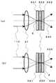
本発明の光制御式光路切替型データ配信装置および配信方法に用いられる光スイッチの最少構成要素からなる光路切替機構91を図5に示す。3つの光路切替機構91、92、および、93を空間的に3段構成で接続した光スイッチ1101の概略構成を図4aに例示する(実施例1参照)。また、本発明で用いられる光スイッチの動作原理を説明するための原理図を図11、図12、図13、および、図14に示す。[Optical switch]
FIG. 5 shows an optical
本発明で用いられる光スイッチ1101は、少なくとも前記信号光(光パケット)120、110、111、112などは透過し、前記制御光(光宛先タグ)121、122、123などの特定の1種類の波長のみを各々選択的に吸収する1つ以上の光吸収層膜兼熱レンズ形成層502などを含む熱レンズ形成素子1などと、前記光吸収層膜の1つ1つに前記制御光と前記信号光とを各々収束させて照射する手段(例えば、集光レンズ31、32、33など)と、前記光吸収層膜を含み、前記光吸収層膜が前記特定の1種類の波長の制御光を吸収した領域およびその周辺領域に起こる温度上昇に起因して可逆的に生ずる屈折率の分布に基づいた熱レンズ50または60を用いることによって、前記特定の1種類の波長の制御光の照射の有無に応じ、図12(b)に示すように前記収束された信号光を収束させたまま出射する、図12(a)に示すように信号光の開き角度を拡大させて出射する、または、図11(a)または図11(b)に示すように信号光を通常の開き角度で出射する1つ以上の熱レンズ形成素子1、2、3などと、前記各熱レンズ形成素子の各々後方に設けられた、穴161と反射手段とを有する穴付ミラー61であって、前記特定の1種類の波長の制御光の照射の有無に応じて、前記熱レンズ形成素子を出射した信号光を前記穴161に通過させ、または、前記反射手段により反射させることによって光路を変化させる鏡61とを備えることを特徴とするものである。 The optical switch 1101 used in the present invention transmits at least the signal light (optical packet) 120, 110, 111, 112, and the like, and a specific type of the control light (optical destination tag) 121, 122, 123, etc. The thermal
以下に、本発明で用いられる光スイッチの構成要素について詳細に説明する。 The components of the optical switch used in the present invention will be described in detail below.
[制御光と信号光とを各々収束させて照射する手段]
本発明で用いられる熱レンズ効果を利用した光スイッチを作動させるに当たり、光吸収層膜兼熱レンズ形成層502の同一領域に制御光と信号光とを各々収束させて照射する手段として、集光レンズあるいは凹面鏡が用いられる。集光レンズとしては通常の凸レンズ31など、非球面凸レンズ、屈折率分布型集光レンズ、複数のレンズからなる顕微鏡用対物レンズ、写真機用レンズ、などを好適に用いることができる。信号光と制御光の波長の相違に応じてレンズ材質の屈折率が異なることに起因する「色収差」を補正するための、屈折率の異なる凸レンズと凹レンズを組み合わせた色収差補正レンズを用いても良い。信号光と制御光を損失なしに光吸収層膜に入射させるためには、集光レンズまたは凹面鏡の有効口径が平行ビームとしての信号光および制御光のビーム径よりも大きくなければならない。また、集光レンズまたは凹面鏡の焦点距離および作動距離(ワーキングディスタンス)に基づいて光吸収層膜との位置関係が設定される。具体例については実施例に記載する。[Means for converging control light and signal light respectively]
In operating the optical switch using the thermal lens effect used in the present invention, as a means for converging and irradiating the control light and the signal light to the same region of the light absorbing layer film / thermal
[受光レンズ]
受光レンズは、制御光が照射されずに収束された信号光が通常の開き角度で熱レンズ形成素子から出射する場合と制御光が照射されて信号光が通常の開き角度よりも拡大された開き角度で熱レンズ形成素子から出射するよう設定された場合に、これらの出射信号光を無駄なく受光し、かつ、平行ビームに戻す手段として用いられる。受光レンズとしては、集光レンズの場合と同様のものを用いることができる。ここで「受光レンズ」という表現を用いたが、凹面鏡を用いることもできる。また、ここで、受光レンズの開口数(以下、「NA」と呼ぶ。)は、集光レンズのNAよりも大きくなるよう設定することが推奨される。具体的には、受光レンズのNAを、集光レンズのNAの2倍以上に設定することによって、信号光が通常の開き角度よりも拡大された開き角度で出射する場合であっても損失なしに受光することが可能となる。[Light receiving lens]
In the light receiving lens, the signal light converged without being irradiated with the control light is emitted from the thermal lens forming element at a normal opening angle, and the signal light is expanded from the normal opening angle by being irradiated with the control light. When it is set to emit from the thermal lens forming element at an angle, it is used as means for receiving these emitted signal lights without waste and returning them to a parallel beam. As the light receiving lens, the same lens as in the case of the condensing lens can be used. Here, the expression “light-receiving lens” is used, but a concave mirror can also be used. Here, it is recommended that the numerical aperture (hereinafter referred to as “NA”) of the light receiving lens is set to be larger than the NA of the condenser lens. Specifically, by setting the NA of the light receiving lens to be twice or more the NA of the condenser lens, there is no loss even when the signal light is emitted at an opening angle that is larger than the normal opening angle. It is possible to receive light.
一方、制御光が照射されたときに収束された信号光が収束されたまま熱レンズ形成素子から出射するよう設定されている場合、出射光のビーム径が細いままであると、後段で再び光スイッチの熱レンズ形成素子へ収束照射する場合や光ファイバーに集光入射させる場合に、光の回析作用によって、充分に収束させることが困難となる。このような場合は収束されたまま出射した信号光をビームエキスパンドしてビーム径を拡大することが推奨される。ビームエキスパンドの手段としては、公知のもの、例えば2枚の凸レンズからなるケプラー型の光学系を用いることができる。 On the other hand, when the signal light converged when the control light is irradiated is set to be emitted from the thermal lens forming element while being converged, if the beam diameter of the emitted light remains thin, the light is re-emitted in the subsequent stage. When convergent irradiation is performed on the thermal lens forming element of the switch or when the light is focused and incident on an optical fiber, it is difficult to sufficiently converge the light due to the diffraction of light. In such a case, it is recommended to expand the beam diameter by expanding the signal light emitted while being converged. As a means for beam expansion, a publicly known one, for example, a Kepler type optical system composed of two convex lenses can be used.
[波長選択透過フィルター]
本発明で用いられる光スイッチ中の熱レンズ形成素子における制御光の透過率が0%でない限り、透過率に相当する分の制御光も熱レンズ形成素子を透過し、出射して来る。この制御光が後段の熱レンズ形成素子等に入射して誤動作ないしクロストークを起こすことを避けるため、熱レンズ形成素子1、2、3などにおける各々の制御光の透過率を0%に限りなく近づける必要がある。更に、熱レンズ形成素子の後方に波長選択透過フィルター(図4において81,82,および83)を、設けることが好ましい。これらの波長選択透過フィルターとしては、個々の制御光の波長帯域の光を完全に遮断し、一方、信号光および後段の光スイッチのための制御光の波長帯域の光を効率良く透過することのできるような波長選択透過フィルターであれば、公知の任意のものを使用することができる。例えば、色素で着色したプラスチックやガラス、表面に誘電体多層膜を設けたガラスなどを用いることができる。このような波長選択透過フィルター用材料からなる薄膜を受光レンズ(図4において41,42,および43)の表面に塗工法、スパッタリング法などの手法で形成し、前記波長選択透過フィルターとしての機能を発揮させても良い。[Wavelength selective transmission filter]
Unless the transmittance of the control light in the thermal lens forming element in the optical switch used in the present invention is 0%, the control light corresponding to the transmittance is also transmitted through the thermal lens forming element and emitted. In order to avoid this control light from entering the subsequent thermal lens forming element or the like and causing malfunction or crosstalk, the transmittance of each control light in the thermal
[熱レンズ形成素子]
本発明において、熱レンズ形成素子としては例えば積層膜型構造を有するものを好適に用いることができ、その積層膜の構成としては例えば以下のような組み合わせを挙げることができる。[Thermal lens forming element]
In the present invention, as the thermal lens forming element, for example, an element having a laminated film type structure can be suitably used, and examples of the laminated film structure include the following combinations.
(1)光吸収層膜単独。ただし、光吸収層膜は、文字通り「光吸収膜」単独の単層膜、あるいは、「光吸収膜/熱レンズ形成層」という2層構造、または、「光吸収膜/熱レンズ形成層/光吸収膜」という3層構造の積層型薄膜のいずれであっても良い。なお、以下の(2)から(10)の「光吸収層膜」も上記同様の構造を含むものとする。 (1) The light absorbing layer film alone. However, the light absorption layer film is literally a single layer film of “light absorption film” alone, or a two-layer structure of “light absorption film / thermal lens formation layer”, or “light absorption film / thermal lens formation layer / light”. Any of the three-layered laminated thin film called “absorbing film” may be used. The following “light absorption layer film” from (2) to (10) includes the same structure as described above.
(2)光吸収層膜/保温層膜 (2) Light absorption layer film / heat insulation layer film
(3)保温層膜/光吸収層膜/保温層膜 (3) Thermal insulation layer film / light absorption layer film / thermal insulation layer film
(4)光吸収層膜/伝熱層膜 (4) Light absorption layer film / heat transfer layer film
(5)伝熱層膜/光吸収層膜/伝熱層膜 (5) Heat transfer layer film / light absorption layer film / heat transfer layer film
(6)光吸収層膜/保温層膜/伝熱層膜 (6) Light absorption layer film / heat insulation layer film / heat transfer layer film
(7)伝熱層膜/光吸収層膜/保温層膜 (7) Heat transfer layer film / light absorption layer film / heat insulation layer film
(8)伝熱層膜/光吸収層膜/保温層膜/伝熱層膜 (8) Heat transfer layer film / light absorption layer film / heat insulation layer film / heat transfer layer film
(9)伝熱層膜/保温層膜/光吸収層膜/保温層膜 (9) Heat transfer layer film / heat insulation layer film / light absorption layer film / heat insulation layer film
(10)伝熱層膜/保温層膜/光吸収層膜/保温層膜/伝熱層膜 (10) Heat transfer layer film / heat insulation layer film / light absorption layer film / heat insulation layer film / heat transfer layer film
(11)屈折率分布型レンズ/(光透過層/)上記(1)ないし(10)の熱レンズ形成素子 (11) Refractive index distribution type lens / (light transmission layer /) thermal lens forming element according to (1) to (10) above
(12)屈折率分布型レンズ/(光透過層/)上記(1)ないし(10)の熱レンズ形成素子/(光透過層/)屈折率分布型レンズ (12) Refractive index distribution type lens / (Light transmission layer /) Thermal lens forming element of (1) to (10) / (Light transmission layer /) Refractive index distribution type lens
なお、上記「(光透過層/)」とは、必要に応じて光透過層を設けることを意味する。更に、必要に応じて光の入射面および出射面に反射防止膜(ARコート膜)を設けても良い。 The above “(light transmissive layer /)” means that a light transmissive layer is provided as necessary. Furthermore, an antireflection film (AR coating film) may be provided on the light incident surface and the light emitting surface as necessary.
熱レンズ形成素子構成の一例を例示した断面図を図11、図12などに示す。図11に例示するように、熱レンズ形成素子1は、制御光121および信号光110の入射側から、例えば、伝熱層膜501/光吸収層膜兼熱レンズ形成層502/伝熱層膜503の順に積層されてなる。 Cross-sectional views illustrating an example of the configuration of the thermal lens forming element are shown in FIGS. As illustrated in FIG. 11, the thermal
また、色素溶液充填式熱レンズ形成素子を例示した模式図を図15に示す。図15に例示するように、色素溶液充填式熱レンズ形成素子800は、伝熱層膜として作用する入射・出射面ガラス801および802、側面ガラス803および804、底面ガラス805に囲まれた光学セル809の色素溶液充填部808へ、導入管806の導入口807から光吸収層膜兼熱レンズ形成層として作用する色素溶液を充填し、導入口807を封じたものである。すなわち、伝熱層膜/光吸収層膜兼熱レンズ形成層/伝熱層膜という素子構成のものである。 FIG. 15 is a schematic diagram illustrating a dye solution-filled thermal lens forming element. As illustrated in FIG. 15, the dye solution-filled thermal
光吸収層膜、熱レンズ形成層、保温層膜、伝熱層膜、光透過層、および屈折率分布型レンズの材料、作成方法、各々の膜厚などについて、以下に、順を追って説明する。 The materials of the light absorption layer film, the thermal lens formation layer, the heat retaining layer film, the heat transfer layer film, the light transmission layer, and the gradient index lens, the manufacturing method, the film thicknesses of each, etc. will be described in order below. .
なお、本発明で用いられる光吸収層膜、熱レンズ形成層、保温層膜、伝熱層膜、光透過層、および屈折率分布型レンズの材料は、その機能に支障をきたさない範囲において、加工性を向上させたり、光学素子としての安定性・耐久性を向上させたりするため、添加物として公知の酸化防止剤、紫外線吸収剤、一重項酸素クエンチャー、分散助剤などを含有しても良い。 In addition, the light absorbing layer film, thermal lens forming layer, heat insulating layer film, heat transfer layer film, light transmission layer, and refractive index distribution type lens material used in the present invention are within the range that does not hinder its function. It contains known antioxidants, UV absorbers, singlet oxygen quenchers, dispersion aids, etc. as additives to improve processability and improve stability and durability as optical elements. Also good.
[光吸収層膜の材料]
本発明で用いられる熱レンズ形成素子中の光吸収層膜に用いられる光吸収性の材料としては、公知の種々のものを使用することができる。[Material of light absorption layer film]
As the light-absorbing material used for the light-absorbing layer film in the thermal lens forming element used in the present invention, various known materials can be used.
本発明で用いられる熱レンズ形成素子中の光吸収層膜に用いられる光吸収性材料の例を具体的に挙げるならば、例えば、GaAs、GaAsP、GaAlAs、InP、InSb、InAs、PbTe、InGaAsP、ZnSeなどの化合物半導体の単結晶、前記化合物半導体の微粒子をマトリックス材料中へ分散したもの、異種金属イオンをドープした金属ハロゲン化物(例えば、臭化カリウム、塩化ナトリウムなど)の単結晶、前記金属ハロゲン化物(例えば、臭化銅、塩化銅、塩化コバルトなど)の微粒子をマトリックス材料中へ分散したもの、銅などの異種金属イオンをドープしたCdS、CdSe、CdSeS、CdSeTeなどのカドミウムカルコゲナイドの単結晶、前記カドミウムカルコゲナイドの微粒子をマトリックス材料中に分散したもの、シリコン、ゲルマニウム、セレン、テルルなどの半導体単結晶薄膜、多結晶薄膜ないし多孔質薄膜、シリコン、ゲルマニウム、セレン、テルルなどの半導体微粒子をマトリックス材料中へ分散したもの、ルビー、アレキサンドライト、ガーネット、Nd:YAG、サファイア、Ti:サファイア、Nd:YLFなど、金属イオンをドープした宝石に相当する単結晶(いわゆるレーザー結晶)、金属イオン(例えば、鉄イオン)をドープしたニオブ酸リチウム(LiNbO3)、LiB3O5、LiTaO3、KTiOPO4、KH2PO4、KNbO3、BaB2O2などの強誘電性結晶、金属イオン(例えば、ネオジウムイオン、エルビウムイオンなど)をドープした石英ガラス、ソーダガラス、ホウケイ酸ガラス、その他のガラスなどのほか、マトリックス材料中に色素を溶解または分散したもの、および、非晶質の色素凝集体を好適に使用することができる。If the example of the light absorptive material used for the light absorption layer film | membrane in the thermal lens formation element used by this invention is specifically mentioned, for example, GaAs, GaAsP, GaAlAs, InP, InSb, InAs, PbTe, InGaAsP, Single crystals of compound semiconductors such as ZnSe, fine particles of the compound semiconductor dispersed in a matrix material, single crystals of metal halides doped with different metal ions (for example, potassium bromide, sodium chloride, etc.), the metal halogens Cadmium chalcogenide single crystals such as CdS, CdSe, CdSeS, and CdSeTe doped with different metal ions such as copper, in which fine particles of a compound (for example, copper bromide, copper chloride, cobalt chloride, etc.) are dispersed in a matrix material, Cadmium chalcogenide fine particles as matrix material Dispersed in, semiconductor single crystal thin film such as silicon, germanium, selenium, tellurium, polycrystalline thin film or porous thin film, semiconductor fine particles such as silicon, germanium, selenium, tellurium dispersed in matrix material, ruby, Alexandrite, Garnet, Nd: YAG, Sapphire, Ti: Sapphire, Nd: YLF, etc. Single crystal (so-called laser crystal) corresponding to gems doped with metal ions, Lithium niobate doped with metal ions (for example, iron ions) (LiNbO3 ), LiB3 O5 , LiTaO3 , KTiOPO4 , KH2 PO4 , KNbO3 , BaB2 O2 and other ferroelectric crystals, metal ions (for example, neodymium ions, erbium ions, etc.) are doped Quartz glass, soda glass, borosilicate glass, In addition to other glass and the like, those obtained by dissolving or dispersing a dye in a matrix material and amorphous dye aggregates can be preferably used.
これらの中でも、マトリックス材料中に色素を溶解または分散したものは、マトリックス材料および色素の選択範囲が広く、かつ熱レンズ形成素子への加工も容易であるため、特に好適に用いることができる。 Among these, those in which a dye is dissolved or dispersed in a matrix material can be used particularly suitably because the selection range of the matrix material and the dye is wide and processing into a thermal lens forming element is easy.
本発明の光制御式光路切替型データ配信装置および配信方法で用いることができる色素の具体例としては、例えば、ローダミンB、ローダミン6G、エオシン、フロキシンBなどのキサンテン系色素、アクリジンオレンジ、アクリジンレッドなどのアクリジン系色素、エチルレッド、メチルレッドなどのアゾ色素、ポルフィリン系色素、フタロシアニン系色素、ナフタロシアニン系色素、3,3’−ジエチルチアカルボシアニンヨージド、3,3’−ジエチルオキサジカルボシアニンヨージドなどのシアニン色素、エチル・バイオレット、ビクトリア・ブルーRなどのトリアリールメタン系色素、ナフトキノン系色素、アントラキノン系色素、ナフタレンテトラカルボン酸ジイミド系色素、ペリレンテトラカルボン酸ジイミド系色素などを好適に使用することができる。 Specific examples of the dye that can be used in the light control type optical path switching type data delivery apparatus and delivery method of the present invention include, for example, xanthene dyes such as rhodamine B, rhodamine 6G, eosin, and phloxine B, acridine orange, and acridine red. Acridine dyes such as azo dyes such as ethyl red and methyl red, porphyrin dyes, phthalocyanine dyes, naphthalocyanine dyes, 3,3′-diethylthiacarbocyanine iodide, 3,3′-diethyloxadicarbo Cyanine dyes such as cyanine iodide, triarylmethane dyes such as ethyl violet and Victoria blue R, naphthoquinone dyes, anthraquinone dyes, naphthalene tetracarboxylic acid diimide dyes, perylene tetracarboxylic acid diimide dyes, etc. It can be used for.
本発明の光制御式光路切替型データ配信装置および配信方法では、これらの色素を単独で、または、2種以上を混合して使用することができる。 In the light control type optical path switching type data distribution apparatus and distribution method of the present invention, these pigments can be used alone or in admixture of two or more.
本発明の光制御式光路切替型データ配信装置および配信方法で用いることのできるマトリックス材料は、
(1)本発明の光制御式光路切替型データ配信装置および配信方法で用いられる光の波長領域で透過率が高いこと、
(2)本発明の光制御式光路切替型データ配信装置および配信方法で用いられる色素または種々の微粒子を安定性良く溶解または分散できること、
という条件を満足するものであれば任意のものを使用することができる。The matrix material that can be used in the light control type optical path switching type data distribution apparatus and distribution method of the present invention,
(1) The transmittance is high in the wavelength region of light used in the light control type optical path switching type data distribution apparatus and distribution method of the present invention,
(2) It is possible to dissolve or disperse dyes or various fine particles used in the light control type optical path switching type data distribution apparatus and distribution method of the present invention with good stability.
Any material can be used as long as the above condition is satisfied.
無機系固体状のマトリックス材料としては、例えば金属ハロゲン化物の単結晶、金属酸化物の単結晶、金属カルコゲナイドの単結晶、石英ガラス、ソーダガラス、ホウケイ酸ガラスなどの他、いわゆるゾルゲル法で作成された低融点ガラス材料などを使用することができる。 Examples of inorganic solid matrix materials include metal halide single crystals, metal oxide single crystals, metal chalcogenide single crystals, quartz glass, soda glass, borosilicate glass, and so-called sol-gel methods. Other low melting glass materials can be used.
無機系液体状のマトリックス材料としては、水、水ガラス(アルカリケイ酸塩の濃厚水溶液)、塩酸、硫酸、硝酸、王水、クロルスルホン酸、メタンスルホン酸、トリフルオロメタンスルホン酸、などを使用することができる。 Water, water glass (concentrated aqueous solution of alkali silicate), hydrochloric acid, sulfuric acid, nitric acid, aqua regia, chlorosulfonic acid, methanesulfonic acid, trifluoromethanesulfonic acid, etc. are used as the inorganic liquid matrix material. be able to.
また、有機系液体状のマトリックス材料として、例えば種々の有機溶剤を使用することができる。有機溶剤としては、具体的には、メタノール、エタノール、イソプロピルアルコール、n−ブタノール、アミルアルコール、シクロヘキサノール、ベンジルアルコールなどのアルコール類、エチレングリコール、ジエチレングリコール、グリセリンなどの多価アルコール類、酢酸エチル、酢酸n−ブチル、酢酸アミル、酢酸イソプロピルなどのエステル類、アセトン、メチルエチルケトン、メチルイソブチルケトン、シクロヘキサノンなどのケトン類、ジエチルエーテル、ジブチルエーテル、メトキシエタノール、エトキシエタノール、ブトキシエタノール、カルビトールなどのエーテル類、テトラヒドロフラン、1、4−ジオキサン、1、3−ジオキソラン、などの環状エーテル類、ジクロロメタン、クロロホルム、四塩化炭素、1、2−ジクロロエタン、1、1、2−トリクロロエタン、トリクレン、ブロモホルム、ジブロモメタン、ジヨードメタン、などのハロゲン化炭化水素類、ベンゼン、トルエン、キシレン、クロロベンゼン、o−ジクロロベンゼン、ニトロベンゼン、アニソール、α−クロロナフタレンなどの芳香族炭化水素類、n−ペンタン、n−ヘキサン、n−ヘプタン、シクロヘキサンなどの脂肪族炭化水素類、N,N−ジメチルホルムアミド、N,N−ジメチルアセトアミド、ヘキサメチルホスホリックトリアミドなどのアミド類、N−メチルピロリドンなどの環状アミド類、テトラメチル尿素、1、3−ジメチル−2−イミダゾリジノンなどの尿素誘導体類、ジメチルスルホキシドなどのスルホキシド類、炭酸エチレン、炭酸プロピレンなどの炭酸エステル類、アセトニトリル、プロピオニトリル、ベンゾニトリルなどのニトリル類、ピリジン、キノリンなどの含窒素複素環化合物類、トリエチルアミン、トリエタノールアミン、ジエチルアミノアルコール、アニリンなどのアミン類、クロル酢酸、トリクロル酢酸、トリフルオロ酢酸、酢酸などの有機酸の他、ニトロメタン、二硫化炭素、スルホランなどの溶剤を用いることができる。これらの溶剤は、また、複数の種類のものを混合して用いても良い。 In addition, as the organic liquid matrix material, for example, various organic solvents can be used. Specific examples of the organic solvent include alcohols such as methanol, ethanol, isopropyl alcohol, n-butanol, amyl alcohol, cyclohexanol, and benzyl alcohol, polyhydric alcohols such as ethylene glycol, diethylene glycol, and glycerin, ethyl acetate, Esters such as n-butyl acetate, amyl acetate, isopropyl acetate, ketones such as acetone, methyl ethyl ketone, methyl isobutyl ketone, cyclohexanone, ethers such as diethyl ether, dibutyl ether, methoxyethanol, ethoxyethanol, butoxyethanol, carbitol , Tetrahydrofuran, 1,4-dioxane, 1,3-dioxolane, and the like, dichloromethane, chloroform, carbon tetrachloride, 1,2- Halogenated hydrocarbons such as chloroethane, 1,1,2-trichloroethane, trichlene, bromoform, dibromomethane, diiodomethane, benzene, toluene, xylene, chlorobenzene, o-dichlorobenzene, nitrobenzene, anisole, α-chloronaphthalene, etc. Aromatic hydrocarbons, n-pentane, n-hexane, n-heptane, aliphatic hydrocarbons such as cyclohexane, amides such as N, N-dimethylformamide, N, N-dimethylacetamide, hexamethylphosphoric triamide , Cyclic amides such as N-methylpyrrolidone, tetramethylurea, urea derivatives such as 1,3-dimethyl-2-imidazolidinone, sulfoxides such as dimethylsulfoxide, carbonates such as ethylene carbonate and propylene carbonate , Nitriles such as acetonitrile, propionitrile and benzonitrile, nitrogen-containing heterocyclic compounds such as pyridine and quinoline, amines such as triethylamine, triethanolamine, diethylaminoalcohol and aniline, chloroacetic acid, trichloroacetic acid and trifluoroacetic acid In addition to organic acids such as acetic acid, solvents such as nitromethane, carbon disulfide, and sulfolane can be used. These solvents may be used by mixing a plurality of types.
更に、有機系のマトリックス材料として、液体状、固体状、ガラス状またはゴム状の有機高分子材料を使用することができる。その具体例としては、ポリスチレン、ポリ(α−メチルスチレン)、ポリインデン、ポリ(4−メチル−1−ペンテン)、ポリビニルピリジン、ポリビニルホルマール、ポリビニルアセタール、ポリビニルブチラール、ポリ酢酸ビニル、ポリビニルアルコール、ポリ塩化ビニル、ポリ塩化ビニリデン、ポリビニルメチルエーテル、ポリビニルエチルエーテル、ポリビニルベンジルエーテル、ポリビニルメチルケトン、ポリ(N−ビニルカルバゾール)、ポリ(N−ビニルピロリドン)、ポリアクリル酸メチル、ポリアクリル酸エチル、ポリアクリル酸、ポリアクリロニトリル、ポリメタクリル酸メチル、ポリメタクリル酸エチル、ポリメタクリル酸ブチル、ポリメタクリル酸ベンジル、ポリメタクリル酸シクロヘキシル、ポリメタクリル酸、ポリメタクリル酸アミド、ポリメタクリロニトリル、ポリアセトアルデヒド、ポリクロラール、ポリエチレンオキシド、ポリプロピレンオキシド、ポリエチレンテレフタレート、ポリブチレンテレフタレート、ポリカーボネート類(ビスフェノール類+炭酸)、ポリ(ジエチレングリコール・ビスアリルカーボネイト)類、6−ナイロン、6,6−ナイロン、12−ナイロン、6,12−ナイロン、ポリアスパラギン酸エチル、ポリグルタミン酸エチル、ポリリジン、ポリプロリン、ポリ(γ−ベンジル−L−グルタメート)、メチルセルロース、エチルセルロース、ベンジルセルロース、ヒドロキシエチルセルロース、ヒドロキシプロピルセルロース、アセチルセルロース、セルローストリアセテート、セルローストリブチレート、アルキド樹脂(無水フタル酸+グリセリン)、脂肪酸変性アルキド樹脂(脂肪酸+無水フタル酸+グリセリン)、不飽和ポリエステル樹脂(無水マレイン酸+無水フタル酸+プロピレングリコール)、エポキシ樹脂(ビスフェノール類+エピクロルヒドリン)、ポリウレタン樹脂、フェノール樹脂、尿素樹脂、メラミン樹脂、キシレン樹脂、トルエン樹脂、グアナミン樹脂などの樹脂、ポリ(フェニルメチルシラン)などの有機ポリシラン、有機ポリゲルマンおよびこれらの共重合・共重縮合体が挙げられる。また、二硫化炭素、四フッ化炭素、エチルベンゼン、パーフルオロベンゼン、パーフルオロシクロヘキサンまたはトリメチルクロロシラン等、通常では重合性のない化合物をプラズマ重合して得た高分子化合物などを使用することができる。更に、これらの有機高分子化合物に色素の残基をモノマー単位の側鎖として、もしくは架橋基として、共重合モノマー単位として、または重合開始末端として結合させたものをマトリックス材料として使用することもできる。更に、前記の色素残基とマトリックス材料が化学結合を形成していても良い。 Furthermore, liquid, solid, glassy or rubbery organic polymer materials can be used as the organic matrix material. Specific examples thereof include polystyrene, poly (α-methylstyrene), polyindene, poly (4-methyl-1-pentene), polyvinylpyridine, polyvinyl formal, polyvinyl acetal, polyvinyl butyral, polyvinyl acetate, polyvinyl alcohol, polychlorinated. Vinyl, polyvinylidene chloride, polyvinyl methyl ether, polyvinyl ethyl ether, polyvinyl benzyl ether, polyvinyl methyl ketone, poly (N-vinyl carbazole), poly (N-vinyl pyrrolidone), polymethyl acrylate, polyethyl acrylate, polyacryl Acid, polyacrylonitrile, polymethyl methacrylate, polyethyl methacrylate, polybutyl methacrylate, polybenzyl methacrylate, polycyclohexyl methacrylate, polymethacrylic acid, Rimethacrylamide, polymethacrylonitrile, polyacetaldehyde, polychloral, polyethylene oxide, polypropylene oxide, polyethylene terephthalate, polybutylene terephthalate, polycarbonates (bisphenols + carbonic acid), poly (diethylene glycol bisallyl carbonate), 6- Nylon, 6,6-nylon, 12-nylon, 6,12-nylon, polyethyl aspartate, ethyl polyglutamate, polylysine, polyproline, poly (γ-benzyl-L-glutamate), methylcellulose, ethylcellulose, benzylcellulose, Hydroxyethyl cellulose, hydroxypropyl cellulose, acetyl cellulose, cellulose triacetate, cellulose tributyrate, alkyd Fat (phthalic anhydride + glycerin), fatty acid-modified alkyd resin (fatty acid + phthalic anhydride + glycerin), unsaturated polyester resin (maleic anhydride + phthalic anhydride + propylene glycol), epoxy resin (bisphenols + epichlorohydrin), polyurethane Resins, phenol resins, urea resins, melamine resins, xylene resins, toluene resins, guanamine resins and other resins, organic polysilanes such as poly (phenylmethylsilane), organic polygermanes, and copolymers / copolycondensates thereof. . In addition, a polymer compound obtained by plasma polymerization of a compound that is not normally polymerizable, such as carbon disulfide, carbon tetrafluoride, ethylbenzene, perfluorobenzene, perfluorocyclohexane, or trimethylchlorosilane, can be used. Furthermore, those obtained by bonding the residue of the dye to these organic polymer compounds as a side chain of the monomer unit, as a crosslinking group, as a copolymerization monomer unit, or as a polymerization initiation terminal can be used as a matrix material. . Further, the dye residue and the matrix material may form a chemical bond.
これらのマトリックス材料中へ色素を溶解または分散させるには公知の方法を用いることができる。例えば、色素とマトリックス材料を共通の溶媒中へ溶解して混合した後、溶媒を蒸発させて除去する方法、ゾルゲル法で製造する無機系マトリックス材料の原料溶液へ色素を溶解または分散させてからマトリックス材料を形成する方法、有機高分子系マトリックス材料のモノマー中へ、必要に応じて溶媒を用いて、色素を溶解または分散させてから該モノマーを重合ないし重縮合させてマトリックス材料を形成する方法、色素と有機高分子系マトリックス材料を共通の溶媒中に溶解した溶液を、色素および熱可塑性の有機高分子系マトリックス材料の両方が不溶の溶剤中へ滴下し、生じた沈殿を濾別し乾燥してから加熱・溶融加工する方法などを好適に用いることができる。色素とマトリックス材料の組み合わせおよび加工方法を工夫することで、色素分子を凝集させ、「H会合体」や「J会合体」などと呼ばれる特殊な会合体を形成させられることが知られているが、マトリックス材料中の色素分子をこのような凝集状態もしくは会合状態を形成する条件で使用しても良い。 Known methods can be used to dissolve or disperse the dye in these matrix materials. For example, the dye and matrix material are dissolved and mixed in a common solvent, then the solvent is evaporated and removed, or the dye is dissolved or dispersed in the raw material solution of the inorganic matrix material produced by the sol-gel method, and then the matrix A method of forming a material, a method of forming a matrix material by dissolving or dispersing a dye in a monomer of an organic polymer matrix material, if necessary, and then polymerizing or polycondensing the monomer; A solution in which a dye and an organic polymer matrix material are dissolved in a common solvent is dropped into a solvent in which both the dye and the thermoplastic organic polymer matrix material are insoluble, and the resulting precipitate is filtered and dried. For example, a method of heating / melting can be preferably used. It is known that by combining the dye and matrix material and processing methods, the dye molecules can be aggregated to form a special aggregate called “H aggregate” or “J aggregate”. The dye molecules in the matrix material may be used under conditions that form such an aggregated state or an associated state.
また、これらのマトリックス材料中へ前記の種々の微粒子を分散させるには公知の方法を用いることができる。例えば、前記微粒子をマトリックス材料の溶液、または、マトリックス材料の前駆体の溶液に分散した後、溶媒を除去する方法、有機高分子系マトリックス材料のモノマー中へ、必要に応じて溶媒を用いて、前記微粒子を分散させてから該モノマーを重合ないし重縮合させてマトリックス材料を形成する方法、微粒子の前駆体として、例えば過塩素酸カドミウムや塩化金などの金属塩を有機高分子系マトリックス材料中へ溶解または分散した後、硫化水素ガスで処理して硫化カドミウムの微粒子を、または、熱処理することで金の微粒子を、それぞれマトリックス材料中に析出させる方法、化学的気相成長法、スパッタリング法などを好適に用いることができる。 A known method can be used to disperse the various fine particles in these matrix materials. For example, after the fine particles are dispersed in a matrix material solution or a matrix material precursor solution, a method of removing the solvent, into the monomer of the organic polymer matrix material, if necessary, using a solvent, A method for forming a matrix material by polymerizing or polycondensing the monomer after dispersing the fine particles, and as a precursor of the fine particles, for example, a metal salt such as cadmium perchlorate or gold chloride into an organic polymer matrix material. After dissolution or dispersion, a method of depositing fine particles of cadmium sulfide by treatment with hydrogen sulfide gas or gold fine particles by heat treatment, a chemical vapor deposition method, a sputtering method, etc. It can be used suitably.
色素を単独で、光散乱の少ない非晶質状態(アモルファス)の薄膜として存在させることができる場合は、マトリックス材料を用いずに、非晶質色素膜を光吸収層膜として用いることもできる。 In the case where the dye can be present alone as an amorphous thin film with little light scattering, an amorphous dye film can also be used as the light absorption layer film without using a matrix material.
また、色素を単独で、光散乱を起こさない微結晶凝集体として存在させることができる場合は、マトリックス材料を用いずに、色素の微結晶凝集体を光吸収層膜として用いることもできる。本発明で用いられる熱レンズ形成素子におけるように、光吸収層膜としての色素微結晶凝集体が、熱レンズ形成層(樹脂など)、伝熱層膜(ガラスなど)および/または保温層膜(樹脂など)と積層されて存在する場合、前記色素微小結晶の粒子径が前記信号光の波長と制御光の波長を比べて短い方の波長の1/5を超えない大きさであれば、実質的に光散乱を起こさない。 In addition, when the dye can be present alone as a microcrystal aggregate that does not cause light scattering, the microcrystal aggregate of the dye can be used as the light absorption layer film without using the matrix material. As in the thermal lens forming element used in the present invention, the dye crystallite aggregate as the light absorbing layer film is formed from a thermal lens forming layer (resin etc.), a heat transfer layer film (glass etc.) and / or a heat insulating layer film ( If the particle size of the dye microcrystal is a size that does not exceed 1/5 of the shorter wavelength compared with the wavelength of the signal light and the wavelength of the control light, Does not cause light scattering.
[光吸収層膜の材料、信号光の波長帯域、および、制御光の波長帯域の組み合わせと順序]
本発明の光制御式光路切替型データ配信装置および配信方法で使用される光吸収層膜の材料、信号光の波長帯域、および制御光の波長帯域は、これらの組み合わせとして、使用目的に応じて適切な組み合わせを選定し用いることができる。[Combination and Order of Light Absorbing Layer Film Material, Signal Light Wavelength Band, and Control Light Wavelength Band]
The material of the light absorption layer film, the wavelength band of the signal light, and the wavelength band of the control light used in the light control type optical path switching type data distribution apparatus and distribution method of the present invention are combinations of these according to the purpose of use. Appropriate combinations can be selected and used.
具体的な設定手順としては、例えば、まず、使用目的に応じて信号光の波長ないし波長帯域を決定し、これを制御するのに最適な光吸収層膜の材料と制御光の波長の組み合わせを選定すれば良い。または、使用目的に応じて信号光と制御光の波長の組み合わせを決定してから、この組み合わせに適した光吸収層膜の材料を選定すれば良い。 As a specific setting procedure, for example, first, the wavelength or wavelength band of signal light is determined according to the purpose of use, and a combination of the material of the light absorption layer film and the wavelength of control light that is optimal for controlling this is selected. It only has to be selected. Alternatively, after determining the combination of the wavelengths of the signal light and the control light according to the purpose of use, a material for the light absorption layer film suitable for this combination may be selected.
このような選定手順の具体例として、信号光としてギガヘルツオーダーで超高速変調可能な半導体レーザーから発振する波長850nm、1350nmあるいは1550nmなどの近赤外線を用い、これを、複数の可視光線波長帯域の制御光で光路切替するケースを以下に例示する。制御光の光源としてはサブミリ秒以下の応答速度で断続可能な連続(CW)発振方式のレーザーを好適に用いることができる。例えば、短波長側から、405ないし445nmの青紫ないし青色半導体レーザー、半導体励起Nd:YAGレーザーの波長1064nmを2次非線形光学素子で532nmの緑色に変換したもの、635ないし670nmの赤色半導体レーザー、および、780ないし800nmの近赤外線レーザーを選定し、好適に使用することができる。これらの制御光波長帯域に吸収を示し、850nmないし1550nmの近赤外線を吸収しない色素として、例えば、N,N’−ビス(2,5−ジ−tert−ブチルフェニル)−3,4,9,10−ペリレンジカルボキシイミド(N,N'-Bis(2,5-di-tert-butylphenyl)-3,4,9,10-perylenedicarboximide)〔1〕、
前記制御光レーザーの発振波長と、これら色素の透過率スペクトルとの関係を表1に示す。 Table 1 shows the relationship between the oscillation wavelength of the control light laser and the transmittance spectrum of these dyes.
表1から判るように、色素〔1〕は波長445ないし532nmの制御光を吸収して熱レンズを形成するような熱レンズ形成素子の光吸収層膜の材料として好適である。同様に色素〔2〕は波長635ないし670nmに対応する光吸収層膜の材料として、また、色素〔3〕は波長780ないし800nmに対応する光吸収層膜の材料として好適である。これらの色素は前記溶剤に溶解させて光学セルへ充填し、または有機高分子材料中に溶解させて伝熱層膜に挟んで、あるいは、伝熱層膜上にスピンコート膜または蒸着膜として成膜して、使用することができる。 As can be seen from Table 1, the dye [1] is suitable as a material for a light absorption layer film of a thermal lens forming element that absorbs control light having a wavelength of 445 to 532 nm to form a thermal lens. Similarly, the dye [2] is suitable as a material for a light absorbing layer film corresponding to a wavelength of 635 to 670 nm, and the dye [3] is suitable as a material for a light absorbing layer film corresponding to a wavelength of 780 to 800 nm. These dyes are dissolved in the solvent and filled into the optical cell, or dissolved in an organic polymer material and sandwiched between the heat transfer layer films, or formed on the heat transfer layer film as a spin coat film or a vapor deposition film. Membrane can be used.
これらの色素を2種類以上選択して使用する場合、各々の色素の吸収波長帯域に対応する熱レンズ形成素子を含む光路切替機構を、吸収波長帯域の短い方から順に連結して使用することが好ましい。すなわち、例えば、第1段目の光路切替機構に色素〔1〕、第2段目に色素〔2〕または〔3〕の2段構成、第1段目に色素〔1〕、第2段目に色素〔2〕、第3段目に色素〔3〕の3段構成として使用することで、各色素の吸収帯域と非吸収帯域を無駄なく重ねて利用することが可能である。 When two or more types of these dyes are selected and used, an optical path switching mechanism including a thermal lens forming element corresponding to the absorption wavelength band of each dye may be used by connecting them in order from the shorter absorption wavelength band. preferable. That is, for example, the first-stage optical path switching mechanism includes the dye [1], the second stage the dye [2] or [3], the two-stage configuration, the first stage the dye [1], the second stage In addition, the dye [2] and the dye [3] in the third stage are used as a three-stage structure, so that the absorption band and the non-absorption band of each dye can be used without waste.
[光吸収層膜の材料の組成、光吸収層膜中の光吸収層膜の膜厚、および熱レンズ形成層の膜厚]
本発明の光制御式光路切替型データ配信装置および配信方法で用いられる熱レンズ形成素子において、光吸収層膜は、「光吸収膜」単独の単層膜、あるいは、「光吸収膜/熱レンズ形成層」という2層構造、または、「光吸収膜/熱レンズ形成層/光吸収膜」という3層構造の積層型薄膜のいずれであっても良く、光吸収層膜全体の厚さは、収束された前記制御光の共焦点距離の2倍を超えないことが好ましい。更に、一層高速な応答速度を目指す場合は、前記積層型薄膜からなる光吸収層膜の厚さは、収束された前記制御光の共焦点距離の1倍を超えないことが好ましい。[Composition of light absorbing layer film material, film thickness of light absorbing layer film in light absorbing layer film, and film thickness of thermal lens forming layer]
In the thermal lens forming element used in the light control type optical path switching type data distribution apparatus and distribution method of the present invention, the light absorption layer film is a single layer film of “light absorption film” alone or “light absorption film / thermal lens”. It may be either a two-layer structure called “formation layer” or a laminated thin film with a three-layer structure called “light absorption film / thermal lens formation layer / light absorption film”. The thickness of the entire light absorption layer film is It is preferable not to exceed twice the confocal distance of the converged control light. Furthermore, when aiming at a higher response speed, it is preferable that the thickness of the light absorption layer film made of the laminated thin film does not exceed one time the confocal distance of the converged control light.
このような条件の中で、本発明で用いられる光吸収層膜の材料の組成および光吸収層膜中の光吸収膜の膜厚については、これらの組み合わせとして、光吸収層膜を透過する制御光および信号光の透過率を基準にして設定することができる。例えば、まず、光吸収層膜の材料の組成の内、少なくとも制御光あるいは信号光を吸収する成分の濃度を決定し、次いで、熱レンズ形成素子を透過する制御光および信号光の透過率が特定の値になるよう光吸収層膜中の光吸収膜の膜厚を設定することができる。または、まず、例えば装置設計上の必要に応じて、光吸収層膜中の光吸収膜の膜厚を特定の値に設定した後、熱レンズ形成素子を透過する制御光および信号光の透過率が特定の値になるよう光吸収層膜の材料の組成を調整することができる。 Under such conditions, the composition of the material of the light absorption layer film used in the present invention and the thickness of the light absorption film in the light absorption layer film are combined to control the transmission through the light absorption layer film. It can be set based on the transmittance of light and signal light. For example, first, determine the concentration of at least the component that absorbs control light or signal light in the composition of the material of the light absorption layer film, and then specify the transmittance of control light and signal light that passes through the thermal lens forming element. The film thickness of the light absorption film in the light absorption layer film can be set so as to be a value of. Alternatively, first, for example, according to the device design, after setting the film thickness of the light absorption film in the light absorption layer film to a specific value, the transmittance of the control light and the signal light transmitted through the thermal lens forming element The composition of the material of the light absorption layer film can be adjusted so that becomes a specific value.
本発明の光制御式光路切替型データ配信装置および配信方法で用いられる熱レンズ形成素子から、できる限り低い光パワーで充分な大きさおよび高速度の熱レンズ効果を引き出すために最適な、光吸収層膜を透過する制御光および信号光の透過率の値は、それぞれ、次に示す通りである。 Light absorption that is optimal for extracting a thermal lens effect of sufficient size and high speed with as low light power as possible from the thermal lens forming element used in the light control type optical path switching type data distribution apparatus and distribution method of the present invention The values of the transmittance of the control light and the signal light that pass through the layer film are as follows, respectively.
本発明の光制御式光路切替型データ配信装置および配信方法で用いられる熱レンズ形成素子においては、熱レンズ形成素子中の光吸収層膜を伝播する制御光の透過率が90%ないし0%になるよう光吸収層膜中の光吸収成分の濃度および存在状態の制御、光吸収層膜中の光吸収膜の膜厚設定を行うことが推奨される。 In the thermal lens forming element used in the light control type optical path switching type data distribution apparatus and distribution method of the present invention, the transmittance of the control light propagating through the light absorbing layer film in the thermal lens forming element is 90% to 0%. It is recommended to control the concentration and existence state of the light absorption component in the light absorption layer film and to set the film thickness of the light absorption film in the light absorption layer film.
一方、制御光を照射しない状態において、熱レンズ形成素子中の光吸収層膜を伝播する信号光の透過率が下限として10%以上、また、上限としては100%に限りなく近づくよう光吸収層膜中の光吸収成分の濃度および存在状態の制御、光吸収層膜中の光吸収膜の膜厚設定を行うことが推奨される。 On the other hand, in a state where the control light is not irradiated, the light absorption layer is such that the transmittance of the signal light propagating through the light absorption layer film in the thermal lens forming element approaches 10% or more as a lower limit and 100% as an upper limit. It is recommended to control the concentration and existence state of the light absorption component in the film and to set the film thickness of the light absorption film in the light absorption layer film.
光吸収層膜中の熱レンズ形成層膜厚の下限は、以下に記載するように、熱レンズ形成層の材料に応じて選定される。 The lower limit of the thermal lens forming layer thickness in the light absorbing layer film is selected according to the material of the thermal lens forming layer as described below.
[光吸収層膜中の熱レンズ形成層の材料および熱レンズ形成層の膜厚]
単層の光吸収膜そのものを、熱レンズ形成層として作用させても良いが、光吸収と熱レンズ形成の機能を別々の材料に分担させて、各々選択された最適の材料を積層して使用することもできる。[Material of thermal lens forming layer in light absorbing layer film and film thickness of thermal lens forming layer]
The single-layer light absorption film itself may act as a thermal lens formation layer, but the functions of light absorption and thermal lens formation are shared by different materials, and each selected optimum material is used in layers. You can also
光吸収層膜中の熱レンズ形成層の材料としては液体、液晶、および、固体の材料を用いることができる。特に、熱レンズ形成層が、非晶質の有機化合物、有機化合物液体、および液晶からなる群から選ばれる有機化合物からなると好適である。なお、熱レンズ形成層の材質が液晶および液体の場合、例えば、光吸収膜および/または伝熱層膜を自己形態保持性の材質で作成し、熱レンズ形成層の厚さに相当する空乏を設け、そこへ流動状態の熱レンズ形成層材料を注入することで、熱レンズ形成層を作成することができる。一方、熱レンズ形成層の材質が固体の場合は、熱レンズ形成層の片面または両面に光吸収膜を積層させて作成すれば良い。 As the material of the thermal lens forming layer in the light absorption layer film, liquid, liquid crystal, and solid material can be used. In particular, the thermal lens forming layer is preferably made of an organic compound selected from the group consisting of an amorphous organic compound, an organic compound liquid, and a liquid crystal. When the material of the thermal lens forming layer is liquid crystal or liquid, for example, a light absorption film and / or a heat transfer layer film is made of a self-form-retaining material, and depletion corresponding to the thickness of the thermal lens forming layer is achieved. A thermal lens forming layer can be created by providing and injecting a thermal lens forming layer material in a fluid state there. On the other hand, when the material of the thermal lens forming layer is solid, the thermal lens forming layer may be formed by laminating a light absorbing film on one or both sides of the thermal lens forming layer.
熱レンズ形成層の材質は単一でなくとも良く、例えば、複数種類の固体の積層膜であっても良く、また、固体と液体を積層させたものであっても良い。 The thermal lens forming layer may not be made of a single material, and may be, for example, a laminated film of a plurality of types of solids or a laminate of solid and liquid.
熱レンズ形成層の厚さは、用いる材料の種類にもよるが、数ナノメートルから1mmの範囲の厚さであれば良く、数十ナノメートルから数百μmの範囲であれば特に好適である。 Although the thickness of the thermal lens forming layer depends on the type of material used, it may be in the range of several nanometers to 1 mm, and is particularly suitable in the range of several tens of nanometers to several hundreds of micrometers. .
前述のように、熱レンズ形成層と1または2枚の光吸収膜を積層してなる光吸収層膜の合計の厚さは、収束された前記制御光の共焦点距離の2倍を超えないことが好ましい。 As described above, the total thickness of the light absorption layer film formed by laminating the thermal lens forming layer and one or two light absorption films does not exceed twice the confocal distance of the converged control light. It is preferable.
光吸収層膜中の熱レンズ形成層の材料としては液体、液晶、および、固体の材料を用いることができるが、いずれの場合も屈折率の温度依存性が大きい材料が好ましい。 As the material for the thermal lens forming layer in the light absorption layer film, liquid, liquid crystal, and solid material can be used. In any case, a material having a large temperature dependence of the refractive index is preferable.
代表的な有機化合物液体および水の屈折率温度依存性の物性値は文献[D.Solimini:J.Appl.Phys.,vol.37,3314(1966)]に記載されている。波長633nmの光に対する屈折率の温度変化[単位:1/K]は、水(0.8×10-4)よりもメタノール(3.9×10-4)などのアルコールが大きく、更に、シクロペンタン(5.7×10-4)、クロロホルム(5.8×10-4)、ベンゼン(6.4×10-4)、二硫化炭素(7.7×10-4)などの非水素結合性有機溶剤が大きい。The refractive index temperature-dependent physical property values of typical organic compound liquids and water are described in the literature [D. Solimini: J. Appl. Phys., Vol. 37, 3314 (1966)]. The temperature change [unit: 1 / K] of the refractive index with respect to light having a wavelength of 633 nm is larger in alcohol such as methanol (3.9 × 10⁻⁴ ) than in water (0.8 × 10⁻⁴ ). Non-hydrogen bonds such as pentane (5.7 × 10⁻⁴ ), chloroform (5.8 × 10⁻⁴ ), benzene (6.4 × 10⁻⁴ ), carbon disulfide (7.7 × 10⁻⁴ ) Large organic solvent.
光吸収層膜中の熱レンズ形成層の材料として液晶を用いる場合、液晶としては、公知の任意のものを使用することができる。具体的には、種々のコレステロール誘導体、4’−n−ブトキシベンジリデン−4−シアノアニリン、4’−n−ヘキシルベンジリデン−4−シアノアニリンなどの4’−アルコキシベンジリデン−4−シアノアニリン類、4’−エトキシベンジリデン−4−n−ブチルアニリン、4’−メトキシベンジリデンアミノアゾベンゼン、4−(4’−メトキシベンジリデン)アミノビフェニル、4−(4’−メトキシベンジリデン)アミノスチルベンなどの4’−アルコキシベンジリデンアニリン類、4’−シアノベンジリデン−4−n−ブチトキシアニリン、4’−シアノベンジリデン−4−n−ヘキシルオキシアニリンなどの4’−シアノベンジリデン−4−アルコキシアニリン類、4’−n−ブトキシカルボニルオキシベンジリデン−4−メトキシアニリン、p−カルボキシフェニル・n−アミルカーボネイト、n−ヘプチル・4−(4’−エトキシフェノキシカルボニル)フェニルカーボネイトなどの炭酸エステル類、4−n−ブチル安息香酸・4’−エトキシフェニル、4−n−ブチル安息香酸・4’−オクチルオキシフェニル、4−n−ペンチル安息香酸・4’−ヘキシルオキシフェニルなどの4−アルキル安息香酸・4’−アルコキシフェニルエステル類、4,4’−ジ−n−アミルオキシアゾキシベンゼン、4,4’−ジ−n−ノニルオキシアゾキシベンゼンなどのアゾキシベンゼン誘導体、4−シアノ−4’−n−オクチルビフェニル、4−シアノ−4’−n−ドデシルビフェニルなどの4−シアノ−4’−アルキルビフェニル類などの液晶、および(2S,3S)−3−メチル−2−クロロペンタノイック酸・4’,4”−オクチルオキシビフェニル、4’−(2−メチルブチル)ビフェニル−4−カルボン酸・4−ヘキシルオキシフェニル、4’−オクチルビフェニル−4−カルボン酸・4−(2−メチルブチル)フェニルなどの強誘電性液晶を使用することができる。 When liquid crystal is used as the material of the thermal lens forming layer in the light absorption layer film, any known liquid crystal can be used. Specifically, various cholesterol derivatives, 4′-n-butoxybenzylidene-4-cyanoaniline, 4′-alkoxybenzylidene-4-cyanoanilines such as 4′-n-hexylbenzylidene-4-cyanoaniline, 4 4'-alkoxybenzylidene such as' -ethoxybenzylidene-4-n-butylaniline, 4'-methoxybenzylideneaminoazobenzene, 4- (4'-methoxybenzylidene) aminobiphenyl, 4- (4'-methoxybenzylidene) aminostilbene Anilines, 4′-cyanobenzylidene-4-n-butoxyaniline, 4′-cyanobenzylidene-4-alkoxyanilines such as 4′-cyanobenzylidene-4-n-hexyloxyaniline, 4′-n-butoxy Carbonyloxybenzylidene-4- Carbonates such as toxaniline, p-carboxyphenyl n-amyl carbonate, n-heptyl 4- (4′-ethoxyphenoxycarbonyl) phenyl carbonate, 4-n-butylbenzoic acid 4′-ethoxyphenyl, 4 4-alkylbenzoic acids, 4′-alkoxyphenyl esters such as 4-n-butylbenzoic acid, 4′-octyloxyphenyl, 4-n-pentylbenzoic acid, 4′-hexyloxyphenyl, 4,4′-di Azoxybenzene derivatives such as -n-amyloxyazoxybenzene, 4,4'-di-n-nonyloxyazoxybenzene, 4-cyano-4'-n-octylbiphenyl, 4-cyano-4'-n Liquid crystals such as 4-cyano-4′-alkylbiphenyls such as dodecylbiphenyl, and (2S, 3S) 3-methyl-2-chloropentanoic acid • 4 ′, 4 ″ -octyloxybiphenyl, 4 ′-(2-methylbutyl) biphenyl-4-carboxylic acid • 4-hexyloxyphenyl, 4′-octylbiphenyl-4 -Ferroelectric liquid crystal such as carboxylic acid 4- (2-methylbutyl) phenyl can be used.
光吸収層膜中の熱レンズ形成層の材料として固体の材料を用いる場合は、光散乱が小さく屈折率の温度依存性の大きな、非晶質の有機化合物が特に好適である。具体的には、前記マトリックス材料と同様に、種々の有機高分子材料の中から光学用樹脂として公知のものを選定して使用することができる。文献[技術情報協会編、「最新光学用樹脂の開発、特性と高精度部品の設計、成形技術」、技術情報協会(1993)、P.35]に記載されている光学用樹脂の屈折率の温度変化[単位:1/K]は、例えば、ポリ(メタクリル酸メチル)が1.2×10-4、ポリカーボネートが1.4×10-4、ポリスチレンが1.5×10-4である。これらの樹脂を光吸収層膜中の熱レンズ形成層の材料として好適に使用することができる。When a solid material is used as the material of the thermal lens forming layer in the light absorption layer film, an amorphous organic compound having a small light scattering and a large temperature dependency of the refractive index is particularly suitable. Specifically, similar to the matrix material, a known optical resin can be selected from various organic polymer materials and used. The refractive index of optical resins described in the literature [Technical Information Association, "Development of the latest optical resins, design of properties and high precision parts, molding technology", Technical Information Association (1993), p. 35] The temperature change [unit: 1 / K] is, for example, 1.2 × 10⁻⁴ for poly (methyl methacrylate), 1.4 × 10⁻⁴ for polycarbonate, and 1.5 × 10⁻⁴ for polystyrene. These resins can be suitably used as a material for the thermal lens forming layer in the light absorption layer film.
前記有機溶剤の屈折率温度依存性は前記光学用樹脂の場合よりも大きいというメリットがある反面、制御光照射による温度上昇が有機溶剤の沸点に到達すると沸騰してしまうという問題がある(高沸点の溶剤を用いる場合は問題ない)。これに対して、揮発性不純物を徹底的に除去した光学用樹脂は、例えばポリカーボネートの場合、制御光照射による温度上昇が250℃を超えるような過酷な条件においても使用可能である。 While the refractive index temperature dependence of the organic solvent has a merit that it is greater than that of the optical resin, there is a problem that the organic solvent boils when the temperature rise due to the control light irradiation reaches the boiling point of the organic solvent (high boiling point). No problem when using other solvents). On the other hand, the optical resin from which volatile impurities have been thoroughly removed can be used even under severe conditions in which, for example, polycarbonate, the temperature rise due to control light irradiation exceeds 250 ° C.
[保温層膜]
保温層膜として気体を用いる場合は、空気の他、窒素、ヘリウム、ネオン、アルゴンなどの不活性ガスを好適に用いることができる。[Heat insulation layer film]
When a gas is used as the heat insulating layer film, an inert gas such as nitrogen, helium, neon, or argon can be suitably used in addition to air.
保温層膜として液体を用いる場合は、熱伝導率が光吸収層膜と同等か光吸収層膜よりも小さい材質であって、かつ、制御光および信号光を透過し、光吸収層膜の材質を溶解または腐食しないものであれば、任意の液体を用いることができる。例えば、光吸収層膜がシアニン色素を含有したポリメタクリル酸メチルからなる場合、流動性パラフィンを用いることができる。 When a liquid is used as the heat insulating layer film, the material having the thermal conductivity equal to or smaller than that of the light absorbing layer film and transmitting control light and signal light, and the material of the light absorbing layer film As long as it does not dissolve or corrode, any liquid can be used. For example, when the light absorption layer film is made of polymethyl methacrylate containing a cyanine dye, fluid paraffin can be used.
保温層膜として固体を用いる場合は、熱伝導率が光吸収層膜(光吸収膜および熱レンズ形成層)と同等か光吸収層膜よりも小さい材質であって、かつ、制御光および信号光を透過し、光吸収層膜や伝熱層膜の材質と反応しないものであれば、任意の固体を用いることができる。例えば、光吸収膜がシアニン色素を含有したポリメタクリル酸メチルからなる場合、色素を含まないポリメタクリル酸メチル[300Kにおける熱伝導率0.15Wm-1K-1]を保温層膜として用いることができる。When a solid is used as the heat insulating layer film, the thermal conductivity is equal to or smaller than that of the light absorbing layer film (light absorbing film and thermal lens forming layer), and the control light and signal light are used. Any solid can be used as long as it does not react with the material of the light absorption layer film or heat transfer layer film. For example, when the light absorbing film is made of polymethyl methacrylate containing a cyanine dye, polymethyl methacrylate [thermal conductivity at 300 K of 0.15 Wm−1 K−1 ] containing no dye is used as the heat insulating layer film. it can.
[伝熱層膜の材料]
伝熱層膜としては、熱伝導率が光吸収層膜よりも大きい材質が好ましく、制御光および信号光を透過し、光吸収層膜や保温層膜の材質と反応しないものであれば、任意のものを用いることができる。熱伝導率が高く、かつ、可視光線の波長帯域における光吸収が小さい材質として、例えば、ダイアモンド[300Kにおける熱伝導率900Wm-1K-1]、サファイア[同46Wm-1K-1]、石英単結晶[c軸に平行方向で同10.4Wm-1K-1]、石英ガラス[同1.38Wm-1K-1]、硬質ガラス[同1.10Wm-1K-1]などを伝熱層膜として好適に用いることができる。[Material of heat transfer layer film]
As the heat transfer layer film, a material having higher thermal conductivity than the light absorption layer film is preferable, and any material can be used as long as it transmits control light and signal light and does not react with the material of the light absorption layer film or the heat insulation layer film. Can be used. Examples of materials having high thermal conductivity and low light absorption in the visible wavelength band include diamond [thermal conductivity at 300
[光透過層の材料]
本発明で用いられる熱レンズ形成素子は、前記制御光の収束手段としての屈折率分布型レンズが、光透過層を介して前記制御光の入射側に積層されて設けられていても良いが、光透過層の材質としては、固体の保温層膜および/または伝熱層膜の材質と同様のものを使用することができる。光透過層は、文字通り、前記制御光および信号光を効率良く透過させるだけでなく、屈折率分布型レンズを熱レンズ形成素子構成要素として接着するためのものである。いわゆる紫外線硬化型樹脂や電子線硬化型樹脂の内、前記制御光および信号光の波長帯域の光透過率の高いものを特に好適に用いることができる。[Material of light transmission layer]
The thermal lens forming element used in the present invention may be provided with a refractive index distribution type lens as the control light converging means laminated on the incident side of the control light via a light transmission layer, As the material of the light transmission layer, the same material as the material of the solid heat insulating layer film and / or the heat transfer layer film can be used. The light-transmitting layer literally transmits the control light and signal light efficiently, and also bonds the gradient index lens as a thermal lens forming element component. Among so-called ultraviolet curable resins and electron beam curable resins, those having a high light transmittance in the wavelength bands of the control light and the signal light can be particularly preferably used.
[熱レンズ形成素子の作成方法]
本発明で用いられる熱レンズ形成素子の作成方法は、熱レンズ形成素子の構成および使用する材料の種類に応じて任意に選定され、公知の方法を用いることができる。[Method for creating thermal lens forming element]
The method for producing the thermal lens forming element used in the present invention is arbitrarily selected according to the configuration of the thermal lens forming element and the type of material used, and a known method can be used.
例えば、熱レンズ形成素子中の光吸収膜に用いられる光吸収性の材料が、前述のような単結晶の場合、単結晶の切削・研磨加工によって、光吸収膜を作成することができる。 For example, when the light absorbing material used for the light absorbing film in the thermal lens forming element is a single crystal as described above, the light absorbing film can be formed by cutting and polishing the single crystal.
例えば、色素を含有したマトリックス材料からなる光吸収膜、光学用樹脂からなる熱レンズ形成層、および光学ガラスを伝熱層膜として組み合わせて用いた「伝熱層膜/光吸収膜/熱レンズ形成層/光吸収膜/伝熱層膜」という構成の熱レンズ形成素子を作成する場合、以下に列挙するような方法によって、まず、伝熱層膜上に光吸収膜を作成することができる。 For example, “heat transfer layer film / light absorption film / thermal lens formation using a light absorbing film made of a matrix material containing a dye, a thermal lens forming layer made of an optical resin, and optical glass as a heat transfer layer film” When a thermal lens forming element having a configuration of “layer / light absorption film / heat transfer layer film” is formed, a light absorption film can be first formed on the heat transfer layer film by the following method.
色素およびマトリックス材料を溶解した溶液を、伝熱層膜として用いられるガラス板上に塗布法、ブレードコート法、ロールコート法、スピンコート法、ディッピング法、スプレー法などの塗工法で塗工するか、あるいは、平版、凸版、凹版、孔版、スクリーン、転写などの印刷法で印刷して光吸収膜を形成する方法を用いても良い。この場合、光吸収膜の形成にゾルゲル法による無機系マトリックス材料作成方法を利用することもできる。 Whether a solution in which a dye and a matrix material are dissolved is applied to a glass plate used as a heat transfer layer film by a coating method such as a coating method, a blade coating method, a roll coating method, a spin coating method, a dipping method, or a spray method. Alternatively, a method of forming a light-absorbing film by printing using a printing method such as a planographic plate, a relief plate, an intaglio plate, a stencil plate, a screen, or a transfer may be used. In this case, an inorganic matrix material preparation method by a sol-gel method can be used for forming the light absorption film.
電着法、電解重合法、ミセル電解法(特開昭63−243298号公報)などの電気化学的成膜手法を用いることができる。 Electrochemical film formation methods such as electrodeposition, electropolymerization, and micelle electrolysis (Japanese Patent Laid-Open No. 63-243298) can be used.
更に、水の上に形成させた単分子膜を移し取るラングミア・ブロジェット法を用いることができる。 Furthermore, the Langmere-Blodgett method which transfers the monomolecular film formed on water can be used.
原料モノマーの重合ないし重縮合反応を利用する方法として、例えば、モノマーが液体の場合、キャスティング法、リアクション・インジェクション・モールド法、プラズマ重合法、および、光重合法などが挙げられる。 Examples of the method utilizing polymerization or polycondensation reaction of raw material monomers include casting method, reaction injection molding method, plasma polymerization method, and photopolymerization method when the monomer is liquid.
昇華転写法、蒸着法、真空蒸着法、イオンビーム法、スパッタリング法、プラズマ重合法、CVD法、有機分子線蒸着法、などの方法を用いることもできる。 Sublimation transfer methods, vapor deposition methods, vacuum vapor deposition methods, ion beam methods, sputtering methods, plasma polymerization methods, CVD methods, organic molecular beam vapor deposition methods, and the like can also be used.
2成分以上の有機系光学材料を溶液または分散液状態で各成分毎に設けた噴霧ノズルから高真空容器内に噴霧して基板上に堆積させ、加熱処理することを特徴とする複合型光学薄膜の製造方法(特許公報第2599569号)を利用することもできる。 A composite optical thin film characterized in that an organic optical material having two or more components is sprayed into a high vacuum container from a spray nozzle provided for each component in a solution or dispersion state, deposited on a substrate, and heat-treated. The manufacturing method (Patent Publication No. 2599569) can also be used.
以上のような固体の光吸収膜の作成方法は、例えば、固体の有機高分子材料からなる保温層膜を作成する場合にも、好適に使用することができる。 The method for producing a solid light-absorbing film as described above can be suitably used when, for example, a heat insulating layer film made of a solid organic polymer material is produced.
次いで、熱可塑性の光学用樹脂を用いて熱レンズ形成層を作成する場合、真空ホットプレス法(特開平4−99609号公報)を用いて「伝熱層膜/光吸収膜/熱レンズ形成層/光吸収膜/伝熱層膜」という構成の熱レンズ形成素子を作成することができる。すなわち、熱可塑性光学用樹脂の粉末またはシートを、上記の方法で表面に光吸収膜を形成した2枚の伝熱層膜(ガラス板)で挟み、高真空下、加熱・プレスすることによって、上記構成の積層型薄膜素子を作成することができる。 Next, when forming a thermal lens forming layer using a thermoplastic optical resin, a vacuum hot pressing method (Japanese Patent Laid-Open No. 4-99609) is used. A thermal lens forming element having a configuration of “/ light absorption film / heat transfer layer film” can be produced. That is, by sandwiching a thermoplastic optical resin powder or sheet between two heat transfer layer films (glass plates) having a light absorbing film formed on the surface by the above method, heating and pressing under high vacuum, A laminated thin film element having the above-described configuration can be produced.
[光学セル]
色素溶液充填式熱レンズ形成素子で用いられる光学セルは、色素溶液を保持する機能、および色素溶液に実効的に形態を付与し、光吸収層膜兼熱レンズ形成層として作用させる機能を有し、更に、収束されて照射される信号光および制御光を受光して前記光応答性組成物へ前記信号光および前記制御光を伝搬させる機能、および前記光応答性組成物を透過した後、発散していく前記信号光を伝搬させて出射する機能を有するものである。[Optical cell]
The optical cell used in the dye solution-filled thermal lens forming element has a function of holding the dye solution and a function of effectively giving the dye solution a form and acting as a light absorption layer film and a thermal lens forming layer. Further, the function of receiving the signal light and the control light that are converged and irradiated to propagate the signal light and the control light to the photoresponsive composition, and the light divergence after passing through the photoresponsive composition It has a function of propagating and emitting the signal light.
色素溶液充填式熱レンズ形成素子で用いられる光学セルの形態は外部形態と内部形態に大別される。 The form of the optical cell used in the dye solution-filled thermal lens forming element is roughly classified into an external form and an internal form.
光学セルの外部形態は、本発明の光制御式光路切替型データ配信装置の構成に応じて、板状、直方体状、円柱状、半円柱状、四角柱状、三角柱状、などの形状のものが用いられる。 The external form of the optical cell may be a plate, rectangular parallelepiped, cylindrical, semi-cylindrical, quadrangular, triangular, etc., depending on the configuration of the optically controlled optical path switching type data distribution device of the present invention. Used.
光学セルの内部形態とは、すなわち、色素溶液充填部の形態であり、色素溶液に、実効的に形態を付与するものである。本発明の光制御式光路切替型データ配信装置の構成に応じて、光学セルの内部形態は、具体的には、例えば、薄膜、厚膜、板状、直方体状、円柱状、半円柱状、四角柱状、三角柱状、凸レンズ状、凹レンズ状、などの中から適宜選択することができる。 The internal form of the optical cell is a form of a dye solution filling portion, and effectively imparts a form to the dye solution. According to the configuration of the light control type optical path switching type data distribution apparatus of the present invention, the internal form of the optical cell is specifically, for example, a thin film, a thick film, a plate, a rectangular parallelepiped, a cylinder, a semi-column, It can be appropriately selected from a quadrangular prism shape, a triangular prism shape, a convex lens shape, a concave lens shape, and the like.
光学セルの構成および材質は、下記の要件を満たすものであれば任意のものを使用することができる。 Any configuration and material of the optical cell can be used as long as they satisfy the following requirements.
(1)上記のような外部形態および内部形態を、使用条件において精密に維持できること。 (1) The external form and the internal form as described above can be accurately maintained under use conditions.
(2)色素溶液に対して不活性であること。 (2) It is inert to the dye solution.
(3)色素溶液を構成する諸成分の放散・透過・浸透による組成変化を防止できること。 (3) It is possible to prevent composition changes due to diffusion, permeation, and penetration of various components constituting the dye solution.
(4)色素溶液が、酸素や水など使用環境に存在する気体あるいは液体と接触することによって劣化することを妨げることができること。 (4) The dye solution can be prevented from deteriorating due to contact with a gas or liquid existing in the use environment such as oxygen or water.
光学セルの材質としては、具体的には、色素溶液の種類によらずソーダガラス、ホウケイ酸ガラスなどの種々の光学ガラス、石英ガラス、サファイアなどを好適に使用することができる。また、色素溶液の溶剤が水やアルコール系である場合、ポリ(メタクリル酸メチル)、ポリスチレン、ポリカーボネートなどのプラスチックを用いることもできる。 Specifically, as the material of the optical cell, various optical glasses such as soda glass and borosilicate glass, quartz glass, sapphire and the like can be suitably used regardless of the type of the dye solution. In addition, when the solvent of the dye solution is water or alcohol, plastics such as poly (methyl methacrylate), polystyrene, and polycarbonate can be used.
なお、上記要件の内、色素溶液の組成変化や劣化を防止する機能は、熱レンズ形成素子としての設計寿命の範囲内に限り発揮できれば良い。 Of the above requirements, the function of preventing the composition change and deterioration of the dye solution only needs to be exhibited within the design life range of the thermal lens forming element.
本発明で用いられる他の光学要素、すなわち、集光レンズ、受光レンズ、波長選択透過フィルターなどを前記光学セルに組み込んだ一体構造の光学セルを用いることができる。 Other optical elements used in the present invention, that is, an optical cell having an integrated structure in which a condensing lens, a light receiving lens, a wavelength selective transmission filter, and the like are incorporated in the optical cell can be used.
[ビームウエスト直径の計算]
本発明の光制御式光路切替型データ配信装置および配信方法において熱レンズ効果を有効に利用するためには、焦点(集光点)近傍の光子密度が最も高い領域、すなわち「ビームウエスト」における前記信号光のビーム断面積が、ビームウエストにおける前記制御光のビーム断面積を超えないように前記信号光および前記制御光のビーム断面の形状および大きさをそれぞれ設定することが好ましい。[Calculation of beam waist diameter]
In order to effectively use the thermal lens effect in the light control type optical path switching type data distribution apparatus and distribution method of the present invention, the above-mentioned region in the region having the highest photon density near the focal point (condensing point), that is, the “beam waist” It is preferable to set the shape and size of the beam cross sections of the signal light and the control light so that the beam cross sectional area of the signal light does not exceed the beam cross sectional area of the control light at the beam waist.
以下、進行方向ビーム断面の電場の振幅分布、すなわち光束のエネルギー分布がガウス分布となっているガウスビームの場合について述べる。なお、以下の説明では、ビーム収束手段として集光レンズ(屈折率分布型レンズ)を用いる場合について説明するが、収束手段が凹面鏡や屈折率分散型レンズであっても同様である。 Hereinafter, the case of a Gaussian beam in which the amplitude distribution of the electric field in the cross section of the traveling direction beam, that is, the energy distribution of the luminous flux is a Gaussian distribution will be described. In the following description, a case where a condensing lens (refractive index distribution type lens) is used as the beam converging unit will be described. However, the same applies when the converging unit is a concave mirror or a refractive index dispersion type lens.
ガウスビームを、図4などの集光レンズ31などで、開き角2θで収束させたときの焦点301近傍における光線束および波面300の様子を図17に示す。ここで、波長λのガウスビームの直径2ωが最小になる位置301を「ビームウエスト」という。以下、ビームウエスト直径を2ω0で表すものとする。光の回折作用のため、2ω0はゼロにはならず、有限の値を持つ。なお、ビーム半径ωやω0の定義は、ガウスビームのビーム中心部分のエネルギーを基準として、エネルギーが1/e2(eは自然対数の底)になる位置をビーム中心から測ったときの距離であり、ビーム直径は2ωまたは2ω0で表される。いうまでもなく、ビームウエストの中心において、光子密度は最も高い。FIG. 17 shows the state of the beam bundle and the
ガウスビームの場合、ビームウエストから充分に遠方でのビーム拡がり角θは波長λおよびビームウエスト径ω0と、次の式〔4〕で関係付けられる。In the case of a Gaussian beam, the beam divergence angle θ sufficiently far from the beam waist is related to the wavelength λ and the beam waist diameter ω0 by the following equation [4].
(数1)
π・θ・ω0 ≒ λ …〔4〕
ここで、πは円周率である。(Equation 1)
π ・ θ ・ ω0 ≒ λ… [4]
Here, π is the circumference ratio.
「ビームウエストから充分に遠方」という条件を満たす場合に限りこの式を用いて、集光レンズに入射するビーム半径ω、集光レンズの開口数および焦点距離から、集光レンズで集光されたビームウエスト径ω0を計算することができる。Only when the condition of “far enough from the beam waist” is satisfied, the light is collected by the condenser lens from the beam radius ω incident on the condenser lens, the numerical aperture of the condenser lens, and the focal length. The beam waist diameter ω0 can be calculated.
更に一般的に、有効開口半径aおよび開口数NAの集光レンズで、ビーム半径ωの平行ガウスビーム(波長λ)を収束させた場合のビームウエスト直径2ω0は、次の式〔5〕で表すことができる。More generally, the beam waist diameter 2ω0 when a parallel Gaussian beam (wavelength λ) having a beam radius ω is converged with a condensing lens having an effective aperture radius a and a numerical aperture NA is expressed by the following equation [5]. Can be represented.
(数2)
2ω0 ≒ k・λ/NA …〔5〕(Equation 2)
2ω0 ≒ k · λ / NA [5]
ここで、係数kは代数的に解くことができないため、レンズ結像面での光強度分布についての数値解析計算を行うことによって決定することができる。 Here, since the coefficient k cannot be solved algebraically, it can be determined by performing a numerical analysis calculation on the light intensity distribution on the lens imaging plane.
集光レンズに入射するビーム半径ωと集光レンズの有効開口半径aの比率を変えて、数値解析計算を行うと、式〔5〕の係数kの値は以下のように求まる。 When numerical analysis calculation is performed by changing the ratio of the beam radius ω incident on the condenser lens and the effective aperture radius a of the condenser lens, the value of the coefficient k in the equation [5] is obtained as follows.
(数3)
a/ω = 1 のとき k ≒ 0.92
a/ω = 2 のとき k ≒ 1.3
a/ω = 3 のとき k ≒ 1.9
a/ω = 4 のとき k ≒ 3(Equation 3)
When a / ω = 1, k≈0.92
When a / ω = 2, k≈1.3
When a / ω = 3, k≈1.9
When a / ω = 4,
すなわち、集光レンズの有効開口半径aよりもビーム半径ωが小さければ小さい程、ビームウエスト径ω0は大きくなる。That is, the smaller the beam radius ω is than the effective aperture radius a of the condenser lens, the larger the beam waist diameter ω0 .
例えば、集光レンズとして開口数0.25、有効開口半径約5mmのレンズを用い、波長780nmの信号光を収束したとき、集光レンズに入射するビーム半径ωが5mmであればa/ωは約1で、ビームウエストの半径ω0は1.4μm、ωが1.25mmであればa/ωは約4でω0は4.7μmと計算される。同様にして波長633nmの制御光を収束したとき、ビーム半径ωが5mmであればa/ωは約1で、ビームウエストの半径ω0は1.2μm、ωが1.25mmであればa/ωは約4でω0は3.8μmと計算される。For example, when a lens having a numerical aperture of 0.25 and an effective aperture radius of about 5 mm is used as a condensing lens and signal light having a wavelength of 780 nm is converged, if the beam radius ω incident on the condensing lens is 5 mm, a / ω is If the beam waist radius ω0 is about 1 and 1.4 μm and ω is 1.25 mm, a / ω is about 4 and ω0 is 4.7 μm. Similarly, when the control light having a wavelength of 633 nm is converged, if the beam radius ω is 5 mm, a / ω is about 1, the beam waist radius ω0 is 1.2 μm, and if ω is 1.25 mm, a / ω is about 4 and ω0 is calculated to be 3.8 μm.
この計算例から明らかなように、集光レンズの焦点近傍の光子密度が最も高い領域、すなわちビームウエストにおける光ビームの断面積を最小にするには、集光レンズに入射する光ビームの強度分布が平面波に近くなるまで、ビーム直径を拡大(ビームエキスパンド)すれば良い。また、集光レンズへ入射するビーム直径が同一の場合、光の波長が短い程、ビームウエスト径は小さくなることも判る。 As can be seen from this calculation example, in order to minimize the cross-sectional area of the light beam in the region where the photon density near the focal point of the condenser lens is the highest, that is, the beam waist, the intensity distribution of the light beam incident on the condenser lens The beam diameter may be expanded (beam expanding) until becomes close to a plane wave. It can also be seen that when the beam diameter incident on the condenser lens is the same, the shorter the wavelength of the light, the smaller the beam waist diameter.
前述のように、本発明の光制御式光路切替型データ配信装置および配信方法において熱レンズ効果を有効に利用するためには、ビームウエスト近傍の光子密度が最も高い領域における前記信号光のビーム断面積が、ビームウエストにおける前記制御光のビーム断面積を超えないように前記信号光および前記制御光のビーム断面の形状および大きさをそれぞれ設定することが好ましい。信号光および制御光ともにガウスビームを用いる場合であれば、以上の説明および計算式にしたがって、集光レンズなどの収束手段で収束する前の平行ビームの状態で、波長に応じて、信号光および制御光のビーム直径を、必要に応じてビームエキスパンドするなどして、調節することによって、ビームウエスト近傍の光子密度が最も高い領域における前記信号光のビーム断面積が、ビームウエストにおける前記制御光のビーム断面積を超えないようにすることができる。前述のようにビームエキスパンドの手段としては、公知のもの、例えば2枚の凸レンズからなるケプラー型の光学系を用いることができる。 As described above, in order to effectively use the thermal lens effect in the optically controlled optical path switching type data distribution apparatus and distribution method of the present invention, the signal light beam is interrupted in the region where the photon density near the beam waist is the highest. It is preferable that the shape and size of the beam cross sections of the signal light and the control light are respectively set so that the area does not exceed the beam cross sectional area of the control light at the beam waist. If a Gaussian beam is used for both the signal light and the control light, in accordance with the above description and calculation formula, the signal light and the state of the parallel beam before being converged by the converging means such as a condenser lens, according to the wavelength. The beam cross-sectional area of the signal light in the region where the photon density in the vicinity of the beam waist is the highest is adjusted by adjusting the beam diameter of the control light, for example, by expanding the beam, if necessary. It is possible not to exceed the beam cross-sectional area. As described above, a known means, for example, a Kepler type optical system composed of two convex lenses can be used as the means for expanding the beam.
[共焦点距離Zcの計算]
一般に、ガウスビームの場合、凸レンズなどの収束手段で収束された光束のビームウエスト近傍、すなわち、焦点を挟んで共焦点距離Zcの区間においては、収束ビームはほぼ平行光と見なすことができ、共焦点距離Zcは、円周率π、ビームウエスト半径ω0および波長λを用いた式〔6〕で表すことができる。[Calculation of confocal distance Zc]
In general, in the case of a Gaussian beam, the convergent beam can be regarded as almost parallel light in the vicinity of the beam waist of the light beam converged by a converging means such as a convex lens, that is, in the section of the confocal distance Zc across the focal point. The focal length Zc can be expressed by the equation [6] using the circumference ratio π, the beam waist radius ω0, and the wavelength λ.
(数4)
Zc = πω02/λ …〔6〕(Equation 4)
Zc = πω02 / λ (6)
式〔6〕のω0に式〔5〕を代入すると、式〔7〕が得られる。Substituting equation [5] into ω0 in equation [6] yields equation [7].
(数5)
Zc ≒ π(k/NA)2λ/4 …〔7〕(Equation 5)
Zc≈π (k / NA)2 λ / 4 (7)
例えば、集光レンズとして開口数0.25、有効開口半径約5mmのレンズを用い、波長780nmの信号光を収束したとき、集光レンズに入射するビーム半径ωが5mmであればa/ωは約1で、ビームウエストの半径ω0は1.4μm、共焦点距離Zcは8.3μm、ωが1.25mmであればa/ωは約4でω0は4.7μm、共焦点距離Zcは88μmと計算される。同様にして波長633nmの制御光を収束したとき、ビーム半径ωが5mmであればa/ωは約1で、ビームウエストの半径ω0は1.2μm、共焦点距離Zcは6.7μm、ωが1.25mmであればa/ωは約4でω0は3.8μm、共焦点距離Zcは71μmと計算される。For example, when a lens having a numerical aperture of 0.25 and an effective aperture radius of about 5 mm is used as a condensing lens and signal light having a wavelength of 780 nm is converged, if the beam radius ω incident on the condensing lens is 5 mm, a / ω is If the beam waist radius ω0 is 1.4 μm, the confocal distance Zc is 8.3 μm, and ω is 1.25 mm, a / ω is about 4, ω0 is 4.7 μm, and the confocal distance Zc. Is calculated to be 88 μm. Similarly, when the control light having a wavelength of 633 nm is converged, if the beam radius ω is 5 mm, a / ω is about 1, the beam waist radius ω0 is 1.2 μm, the confocal distance Zc is 6.7 μm, ω Is 1.25 mm, a / ω is about 4, ω0 is calculated to be 3.8 μm, and the confocal distance Zc is calculated to be 71 μm.
[光吸収層膜の最適膜厚]
光吸収層膜を構成する1または2枚の光吸収膜の厚さを変えず、熱レンズ形成層の厚さを変えて試料を作製し、光学濃度一定で膜厚の異なる複数の熱レンズ形成素子について実験した結果、上記のようにして計算される共焦点距離Zcの2倍を光吸収層膜の膜厚の上限としたとき、熱レンズ効果の光応答速度が充分高速になることが判った。[Optimal film thickness of light absorption layer]
Samples are manufactured by changing the thickness of the thermal lens forming layer without changing the thickness of one or two light absorbing films constituting the light absorbing layer film, and a plurality of thermal lenses having different optical thicknesses with a constant optical density are formed. As a result of experiments on the element, it was found that the light response speed of the thermal lens effect is sufficiently high when the double of the confocal distance Zc calculated as described above is set as the upper limit of the thickness of the light absorption layer film. It was.
光吸収層膜の膜厚の下限については、熱レンズ効果が発揮できる限りにおいて、薄ければ薄いほど好ましい。 About the minimum of the film thickness of a light absorption layer film, as long as the thermal lens effect can be exhibited, it is so preferable that it is thin.
[保温層膜の膜厚]
保温層膜の膜厚には、光応答の大きさおよび/または速度を最大にするような最適値(下限値および上限値)が存在する。その値は熱レンズ形成素子の構成、光吸収層膜の材質および厚さ、保温層膜の材質、伝熱層膜の材質および厚さなどに応じて、実験的に決定することができる。例えば、伝熱層膜として通常のホウケイ酸ガラス、保温層膜および熱レンズ形成層の材質としてポリカーボネート、光吸収膜としてプラチナフタロシアニンの蒸着膜を用い、ガラス(伝熱層膜、膜厚150μm)/ポリカーボネート樹脂層(保温層)/プラチナフタロシアニン蒸着膜(光吸収膜、膜厚0.2μm)/ポリカーボネート樹脂層(熱レンズ形成層、膜厚20μm)/プラチナフタロシアニン蒸着膜(光吸収膜、膜厚0.2μm)/ポリカーボネート樹脂層(保温層)/ガラス(伝熱層膜、膜厚150μm)という構成の熱レンズ形成素子を作成した場合、保温層膜の膜厚は好ましくは5nmから5μmであり、更に好ましくは50nmから500nmである。[Thickness of heat insulation layer film]
There is an optimum value (lower limit value and upper limit value) that maximizes the magnitude and / or speed of the optical response in the film thickness of the heat insulating layer film. The value can be experimentally determined according to the configuration of the thermal lens forming element, the material and thickness of the light absorption layer film, the material of the heat retaining layer film, the material and thickness of the heat transfer layer film, and the like. For example, an ordinary borosilicate glass is used as the heat transfer layer film, polycarbonate is used as the material for the heat insulation layer film and the thermal lens formation layer, and a platinum phthalocyanine vapor deposition film is used as the light absorption film, and glass (heat transfer layer film, film thickness 150 μm) / Polycarbonate resin layer (thermal insulation layer) / platinum phthalocyanine vapor deposition film (light absorption film, film thickness 0.2 μm) / Polycarbonate resin layer (thermal lens formation layer,
[伝熱層膜の膜厚]
伝熱層膜の膜厚にも、光応答の大きさおよび/または速度を最大にするような最適値(この場合は下限値)が存在する。その値は熱レンズ形成素子の構成、光吸収層膜の材質および厚さ、保温層の材質および厚さ、伝熱層膜の材質などに応じて、実験的に決定することができる。例えば、伝熱層膜として通常のホウケイ酸ガラス、保温層膜および熱レンズ形成層の材質としてポリカーボネート、光吸収膜としてプラチナフタロシアニンの蒸着膜を用い、ガラス(伝熱層膜、膜厚150μm)/ポリカーボネート樹脂層(保温層)/プラチナフタロシアニン蒸着膜(光吸収膜、膜厚0.2μm)/ポリカーボネート樹脂層(熱レンズ形成層、膜厚20μm)/プラチナフタロシアニン蒸着膜(光吸収膜、膜厚0.2μm)/ポリカーボネート樹脂層(保温層)/ガラス(伝熱層膜、膜厚150μm)という構成の熱レンズ形成素子を作成した場合、伝熱層膜の厚さの下限は、好ましくは10μm、更に好ましくは100μmである。なお、伝熱層膜の膜厚の上限については光応答の大きさおよび/または速度からの制約はないが、用いられる集光レンズおよび受光レンズの方式、焦点距離および作動距離(ワーキングディスタンス)と整合させて設計する必要がある。[Film thickness of heat transfer layer film]
The film thickness of the heat transfer layer film also has an optimum value (in this case, a lower limit value) that maximizes the magnitude and / or speed of the optical response. The value can be experimentally determined according to the configuration of the thermal lens forming element, the material and thickness of the light absorption layer film, the material and thickness of the heat retaining layer, the material of the heat transfer layer film, and the like. For example, an ordinary borosilicate glass is used as the heat transfer layer film, polycarbonate is used as the material for the heat insulation layer film and the thermal lens formation layer, and a platinum phthalocyanine vapor deposition film is used as the light absorption film, and glass (heat transfer layer film, film thickness 150 μm) / Polycarbonate resin layer (thermal insulation layer) / platinum phthalocyanine vapor deposition film (light absorption film, film thickness 0.2 μm) / Polycarbonate resin layer (thermal lens formation layer,
[熱レンズ効果による光路切替機構の動作原理と態様]
本発明で用いられる光スイッチを構成する最小単位としての光路切替機構91の動作原理を説明するための原理図を図11、図12、図13、および、図14に示す。これらの図において、熱レンズ形成素子1は「伝熱層膜501/光吸収層膜兼熱レンズ形成層502/伝熱層膜503」という積層構造であるとする。また、制御光として用いられるレーザー光のビーム断面の光強度分布がガウス分布である「ガウスビーム」を用いるものとする。ガウスビームを凸レンズなどの集光レンズで収束させると、ビームウエスト(集光点;焦点)での光強度分布も、ガウス分布となる。[Operation principle and mode of optical path switching mechanism by thermal lens effect]
FIG. 11, FIG. 12, FIG. 13 and FIG. 14 show the principle diagrams for explaining the operation principle of the optical
図11に示すように、コリメートされた平行光ビーム110(信号光または制御光)が集光レンズ31によって収束されて熱レンズ形成素子1の光吸収層膜兼熱レンズ形成層502に照射された場合、平行光ビーム110として収束・照射された制御光は光吸収層膜に吸収されて光エネルギーが熱エネルギーに変換され、光吸収の起きた光吸収層膜の近傍および隣接する熱レンズ形成層の温度が上昇、熱膨張し、屈折率は低下する。上記のようにビーム断面の光強度分布がガウス分布となった光を照射すると、光強度の強いガウス分布の中心部分が収束されて照射されたところが「光吸収の中心」となり、その部分の温度が最も高く、かつ、屈折率が一番小さくなる。光吸収の中心部分から外周へ向けての光吸収も熱に変わり、更に周囲に伝搬される熱により熱レンズ形成層を含む光吸収層膜の屈折率が光吸収中心から外部へ向けて球状に変化して、光吸収中心の屈折率が最も低く外部へ向けて屈折率が高くなる分布を生じ、局部的には凹レンズのように機能する。実際には、制御光は集光レンズ31などによって集光されて熱レンズ形成層を含む光吸収層膜中に照射され、光吸収が収束光の進行方向に多重に起こり、多重に形成された熱レンズによって、進行する制御光自身の光束も変形されるため、観測される熱レンズ効果は、以下に述べるように単一の凹レンズによるものとは異なる。 As shown in FIG. 11, the collimated parallel light beam 110 (signal light or control light) is converged by the
光吸収層膜の吸収帯域にある波長の制御光と透過帯域の波長である信号光とを、図11(a)に示すように熱レンズ形成素子1の光吸収層膜の入射面に近い位置5にビームウエスト(焦点)が位置するように同時に照射すると、図12(a)に示すように制御光により入射面に近い位置に形成された熱レンズ50により、信号光は断面がリング状に拡がるように拡散された出射信号光201として通常の出射信号光200よりも大きい開き角度で出射する。熱レンズ形成素子1を出射した出射信号光201または200を約50cm遠方に設置した半透明スクリーンに投射し、背面から撮影した信号光ビーム断面の写真をそれぞれ図18(a)および図18(b)に示す。図18(b)に示すように熱レンズ形成素子1から通常の開き角で出射した信号光200の断面は、前記スクリーン上で直径d2の円形である。これに対して、信号光と制御光を熱レンズ形成素子1の光吸収層膜の入射面に近い位置5において焦点を結ぶように同時に照射したとき制御光により入射面に近い位置に形成された熱レンズ50により断面がリング状に拡がるように拡散された出射信号光201の断面は、図18(a)に示すように、外径d3かつ内径d4のリングとして前記スクリーンに投射される。図18において明らかなように、外径d3かつ内径d4は、ともに制御光が照射されない場合の信号光・円形ビーム直径d2よりも大きい。As shown in FIG. 11A, the control light having the wavelength in the absorption band of the light absorption layer film and the signal light having the wavelength in the transmission band are positioned close to the incident surface of the light absorption layer film of the thermal
一方、図11(b)に示すように熱レンズ形成素子の光吸収層膜の出射面に近い位置6において焦点を結ぶように同時に照射すると、図12(b)に示すように制御光により出射面に近い位置に形成された熱レンズ60により、信号光は収束されたまま出射する信号光119として出射する。熱レンズ形成素子1を出射した出射信号光119を前記半透明スクリーンに投射し、背面から撮影した信号光ビーム断面の写真を図18(c)に示す。信号光と制御光を熱レンズ形成素子1の光吸収層膜の出射面に近い位置6において焦点を結ぶように同時に照射したとき制御光により出射面に近い位置に形成された熱レンズ60により収束されたまま出射する信号光119の断面は、図18(c)に示すように、外径d0の円形として前記スクリーンに投射される。図18において明らかなように、外径d0は、制御光が照射されない場合の信号光・円形ビーム直径d2よりも小さい。なお、収束出射信号光119の輝度は非常に高いため、前記スクリーンへ投射して写真撮影する際、前記スクリーンの手前に減光フィルターを設置してハレーションが起こることを防いだ。On the other hand, when irradiation is performed simultaneously so as to focus at a
図11(a)および図11(b)のいずれの場合も、制御光を照射しないと、図12(a)および図12(b)に点線で示すように信号光は熱レンズ50または60の影響を受けることなく、信号光のみが通常の開き角度の出射光200として出射する。 In either case of FIG. 11 (a) or FIG. 11 (b), if the control light is not irradiated, the signal light is emitted from the
また、熱レンズ効果の有無と熱レンズ形成素子の光吸収層膜におけるビームウエスト(集光点;焦点)位置の相違(入射側か出射側か)に対応した信号光ビーム断面における光強度分布の相違の測定を以下のように行うことができる。すなわち、図4、図13または図14に概要を示す装置において、受光レンズ41の開口数0.55、集光レンズ31の開口数0.25とし、穴付ミラー61の代わりに図19に概要を示すような光強度分布測定器700を設置し、熱レンズ形成素子1を透過した信号光ビームの全てを受光レンズ41で受光し、平行光線として前記光強度分布測定器の受光部701(有効直径20mm)へ入射させ、信号光ビーム断面の光強度分布を測定した。測定結果を図20、図21、および、図22に示す。ここで、光強度分布測定器は、図19に示すように、受光部701(有効直径20mm)に対して幅1mmの第一のスリット702を設け、第一のスリットの長さ方向、すなわち図19において点710から点720の向きに、幅25μmの第二のスリット703を一定速度で移動させて、2枚のスリットが作る1mm×25μmの長方形の窓を通過した光の強度を、前記窓の移動位置に対応させて測定する装置である。前記窓の移動位置に対応させて光強度を測定するには、例えば、第二のスリット703の移動速度に同期させたストレージオシロスコープ上に、前記窓を通過した光を受光した検出器の出力を記録すれば良い。図20〜図22は、以上のようにして、ストレージオシロスコープ上に記録された信号光の光ビーム断面についての光強度分布を示すものであり、横軸(光ビーム断面内の位置)は受光部701の中心を0として、図19の点710を負方向、点720を正方向と座標を定めて表した位置に対応し、縦軸は光強度を表す。 The light intensity distribution in the cross section of the signal light beam corresponding to the presence or absence of the thermal lens effect and the difference (incident side or outgoing side) of the beam waist (condensing point: focal point) position in the light absorbing layer film of the thermal lens forming element. The difference measurement can be made as follows. That is, in the apparatus outlined in FIG. 4, FIG. 13 or FIG. 14, the numerical aperture of the
図20は、図11(a)および図13(a)の場合に対応し、熱レンズ形成素子1に制御光が入射せず、信号光のみが入射した場合の前記信号光ビーム断面の光強度分布である。この場合の光強度分布は、中心部分の強度が強く、周辺にいくにしたがって強度が弱まる分布(おおむね「ガウス分布」)である。したがって、この場合に充分な大きさの穴161を有する穴付ミラー61が図13(a)のように設置されていると、信号光ビーム111の全てが穴付ミラーの穴161を通過することができる。ここで、平行光として集光レンズ31(焦点距離f1)へ入射する信号光のビーム直径をd1、受光レンズ41(焦点距離f2)によって平行光とされた信号光ビーム111のビーム直径をd2とすると、
(数6)
f1:f2=d1:d2 …〔8〕
であるから、d2は次の式によって求めることができる。FIG. 20 corresponds to the cases of FIG. 11A and FIG. 13A, and the light intensity of the cross section of the signal light beam when only the control light is not incident on the thermal
(Equation 6)
f1 : f2 = d1 : d2 (8)
Therefore, d2 can be obtained by the following equation.
(数7)
d2=(f2/f1)×d1 …〔9〕(Equation 7)
d2 = (f2 / f1 ) × d1 (9)
穴付ミラー61は、例えば、信号光の光軸と45度の角度を持って設置されているものとする。また、穴161を通過する信号光の断面は円形である。したがって、穴161の形状は短径D1、長径D2の楕円である必要があり、D1とD2は次の式〔10〕の関係にある。For example, the holed
(数8)
D2=D1×√2 …〔10〕(Equation 8)
D2 = D1 × √2 ... [10]
ここで、穴付ミラー61の楕円形穴161の短径D1は、式〔9〕から求められる信号光ビーム111のビーム直径d2よりも大きければ良い。ただし、D1が大きすぎると制御光の照射によってリング状に拡大された信号光の一部も通過してしまう。すなわち、D1の最適値はd2の1.01倍ないし1.2倍であり、より好ましくは1.02倍ないし1.1倍である。Here, the short diameter D1 of the
図21は、図11(a)、図12(a)および図13に示すような光学配置の場合に対応し、ビームウエスト(集光点;焦点)を熱レンズ形成素子1の集光レンズ31に近い位置5(光の入射側)に設定し、制御光を照射したときの信号光ビーム断面の光強度分布である。この場合の光強度分布は、中心部分の光強度が弱く、周辺でリング状に光強度が増大する分布になっている。信号光ビーム断面の中心部の光強度は、制御光強度および熱レンズ形成素子1と焦点の位置関係に依存して減少し、制御光強度が増すにしたがって、ゼロに近づいていく。また、信号光強度の極大位置は、元のビーム直径よりも大きな値(直径約15mm)であった。 FIG. 21 corresponds to the case of the optical arrangement as shown in FIGS. 11A, 12 A and 13, and the beam waist (condensing point: focal point) is the condensing
図22は、図11(b)、図12(b)および図14に示すような光学配置の場合に対応し、ビームウエスト(集光点;焦点)を熱レンズ形成素子1の受光レンズ41に近い位置6(光の出射側)に設定し、制御光を照射したときの信号光ビーム断面の光強度分布である。この場合は、中心部分の光強度が、制御光を照射しない場合の中心部分の光強度(図21)より強くなっている。この場合、信号光ビーム断面の中心部の光強度は、制御光強度および熱レンズ形成素子1と焦点6との位置関係に依存するが、制御光非照射時の数倍にも達する。 FIG. 22 corresponds to the case of the optical arrangement as shown in FIGS. 11B, 12 B and 14, and the beam waist (condensing point: focal point) is applied to the
したがって、この場合に穴付ミラー61が設置されていると、信号光ビームの大部分が穴付ミラーの穴161を通過する。ここで、穴付ミラー61(および62,63)の穴161の大きさが最適化されていると、穴付ミラー61によって反射される信号光を事実上ゼロにすることができる。しかしながら、穴付ミラー61の穴161の大きさを最適化しても、制御光を照射しない場合、図14(a)に示す信号光111の中心部分が穴161を漏れ信号光118として通過してしまい、クロストークが発生することは防げない。 Therefore, if the
しかるに、熱レンズ形成素子へ入射する信号光ビーム断面の光強度分布を変更することによって、このような漏れ信号光を事実上ゼロにすることができる。すなわち、図6に示すように、光信号路1110から出射した信号光110をコリメートレンズ30を用いて整形した後、円錐プリズム型レンズなどからなるビーム断面リング化レンズ群321によって、信号光ビーム断面の光強度分布を図18(a)および図21に相当するようなリング状の分布にすることが容易にできる。このような断面光強度分布の信号光110を集光レンズ31にて焦点位置6(図14(a))を通過するように収束して熱レンズ形成素子1を透過させた後、受光レンズ41で平行光線に戻すと、その光ビーム断面の光強度分布は図21に相当するように周辺部分で強く、中心部分が事実上ゼロの「リング状」となるため、穴付ミラー61を設置した場合、その穴161を通過する信号光のモレを事実上、なくすことができる。信号光ビーム断面の光強度分布がこのように「リング状」であっても、図14(b)のように制御光を照射して熱レンズ60を過渡的に形成させた場合には、信号光ビーム断面の光強度分布は鋭いビーム状の収束直進信号光119として穴付ミラー61の穴161を通過していく。 However, by changing the light intensity distribution in the cross section of the signal light beam incident on the thermal lens forming element, such leakage signal light can be made practically zero. That is, as shown in FIG. 6, after the
以上、まとめると、図13の光学配置において、制御光照射の有無に対応して、熱レンズ形成素子を通過した信号光のビーム断面の光強度分布が図21のリング状分布(制御光照射の場合)と図20のガウス分布(制御光非照射の場合)の間で切り替えられ、これを、信号光ビーム断面の光強度分布の形状に適合した穴付ミラーによって、それぞれ別個に取り出すことによって、信号光の光路の切替が可能となる。 In summary, in the optical arrangement of FIG. 13, the light intensity distribution of the beam cross section of the signal light that has passed through the thermal lens forming element corresponds to the presence or absence of the control light irradiation. And the Gaussian distribution of FIG. 20 (in the case of no control light irradiation), and this is separately taken out by a mirror with a hole adapted to the shape of the light intensity distribution of the signal light beam cross section, The optical path of the signal light can be switched.
一方、図14に例示するような光学配置において、制御光および信号光の焦点が熱レンズ形成素子の出射側に近い位置6になるよう調整し、更に信号光ビーム断面の光強度分布をリング状にすることによって、制御光非照射のとき、信号光本来の進行方向から90度、光路を切り替えて信号光を出射させること、また、制御光照射時に信号光を直進させることができる。 On the other hand, in the optical arrangement as illustrated in FIG. 14, the control light and the signal light are adjusted so that the focal points of the control light and the signal light are close to the exit side of the thermal lens forming element, and the light intensity distribution of the signal light beam cross section is a ring shape Thus, when the control light is not irradiated, the signal light can be emitted by switching the optical path by 90 degrees from the original traveling direction of the signal light, and the signal light can be caused to travel straight when the control light is irradiated.
[複数の光路切替機構の組み合わせ方法]
熱レンズ入射光の集光レンズ(31など)、熱レンズ形成素子(1など)、熱レンズ出射光の受光レンズ(41など)、波長選択透過フィルター(81など)および穴付ミラー(61など)からなる光路切替機構(91など)を2つ以上、空間結合方式で連結させて使用する場合、出射信号光が通常の開き角度よりも拡大されて出射する動作態様と、収束されたまま出射する動作態様の組み合わせとして、以下の3通りを用いることができる。[Combination method of multiple optical path switching mechanisms]
Thermal lens incident light condensing lens (such as 31), thermal lens forming element (such as 1), thermal lens outgoing light receiving lens (such as 41), wavelength selective transmission filter (such as 81) and holed mirror (such as 61) When two or more optical path switching mechanisms (such as 91) are connected and used in a spatially coupled manner, the outgoing signal light is emitted with an expansion angle larger than the normal opening angle, and is emitted while being converged. The following three types can be used as combinations of operation modes.
(1)出射信号光が通常の開き角度よりも拡大されて出射する動作態様だけの組み合わせ。 (1) A combination of only the operation modes in which the outgoing signal light is emitted with being enlarged from the normal opening angle.
(2)出射信号光が収束されたまま出射する動作態様だけの組み合わせ。 (2) A combination of only operation modes in which the outgoing signal light is emitted while being converged.
(3)出射信号光が通常の開き角度よりも拡大されて出射する動作態様の後段に出射信号光が収束されたまま出射する動作態様を用いる組み合わせ。 (3) A combination using an operation mode in which the emitted signal light is emitted while being converged in a subsequent stage of the operation mode in which the emitted signal light is emitted with an expansion larger than a normal opening angle.
3番目の組み合わせとして、1段目の光路切替機構が制御光と信号光とを、図11(a)に示すように熱レンズ形成素子1の光吸収層膜の入射面に近い位置5にビームウエスト(焦点)が位置するように同時に照射して、出射する信号光が熱レンズ効果によって、通常の開き角よりも拡大されてリング状断面で出射する動作態様の場合、リング状断面の信号光を穴付ミラー61で反射させて光路切替した後に、2段目の光路切替機構として、制御光と信号光とを、図11(b)に示すように熱レンズ形成素子1の光吸収層膜からの出射面に近い位置6にビームウエスト(焦点)が位置するように同時に照射して、出射する信号光が熱レンズ効果によって、収束されたままの小さい断面で出射する動作態様を採用することで、前記ビーム断面リング化レンズ群321を用いることなく、効率良く、2つの光路切替機構を組み合わせることが可能となる。この組み合わせの詳細については実施例4に記載する。 As a third combination, the optical path switching mechanism in the first stage transmits the control light and the signal light to a
[穴付ミラー]
穴付ミラー61は、例えば、信号光の光軸と45度の角度を持って設置されている。穴付ミラー61のミラー面は、ガラス面上に誘電体多層膜をスパッタリング法で作成し、信号光の波長で反射率が極大になるよう調整したものを用いた。穴付ミラー61の穴161の部分は、ガラスに楕円状の穴を、45度傾けて開けて作成した。穴を開ける替わりに、楕円状に反射膜を付けなくても良いが、ガラス面には反射が数%あって信号光の減衰かつクロストークが起こるので、穴を開ける方が好ましい。穴の内面は光散乱などによる迷光を防ぐため、平滑で、無反射処理されていることが好ましい。また、反射膜は、誘電体多層膜に限らず、用いる制御光および信号光を反射する材料であれば良く、金、銀等でも良い。[Hole mirror]
For example, the
[時間分割型「多:1」双方向光通信]
本発明の光制御式光路切替型データ配信装置および配信方法は、使用している光スイッチの動作原理から、当該光スイッチの作動期間のみ、データサーバー装置側と特定のクライアント装置側の光通信経路が双方に「開」となるものである。したがって、特定のクライアント装置側から随時、サーバー側へデータ送信依頼を当該光通信経路を通じて送信できるようにするためには、データサーバー装置側から一定時間毎に繰り返し、個々のクライアント装置へ向けて順番に、少なくとも制御光・光宛先タグを一定時間、送信し続ける必要がある。さもなければ、クライアント装置からデータサーバー装置へ、例えば、別の光通信路を用いての光通信または従来型ローカルエリアネットワークを用いての電気通信を行わなければならない。[Time division type "multiple: 1" bidirectional optical communication]
The optical control type optical path switching type data distribution apparatus and distribution method of the present invention is based on the operating principle of the optical switch used, and the optical communication path between the data server apparatus side and the specific client apparatus side only during the operation period of the optical switch. Is "open" to both sides. Therefore, in order to be able to transmit a data transmission request from the specific client device side to the server side as needed through the optical communication path, the data server device side repeatedly repeats the data server device at regular intervals, and in turn toward each client device. In addition, it is necessary to continue transmitting at least the control light / light destination tag for a certain period of time. Otherwise, for example, optical communication using another optical communication path or electrical communication using a conventional local area network must be performed from the client device to the data server device.
複数のクライアント装置とデータサーバー装置の間の光信号路を一定時間毎に順番に開くことは、すなわち、時間分割型「多:1」双方向光通信である。 Opening optical signal paths between a plurality of client devices and data server devices in order at regular intervals is time-division “multi: 1” bidirectional optical communication.
時間分割の間隔、光パケットのデータ量、光スイッチのON/OFF応答速度、および、クライアント数は相互に関係している。例えば、光スイッチのON/OFF応答速度が充分に早い場合は、時間分割の間隔を短くして、クライアント数を増やしても光パケットのデータ量が不足することはないが、光スイッチのON/OFF応答に時間を要する場合、充分なデータ量を提供可能なクライアント数は制限される。 The time division interval, the optical packet data amount, the ON / OFF response speed of the optical switch, and the number of clients are interrelated. For example, if the ON / OFF response speed of the optical switch is sufficiently high, the data amount of the optical packet will not be insufficient even if the time division interval is shortened and the number of clients is increased. When time is required for the OFF response, the number of clients that can provide a sufficient amount of data is limited.
実施例に記載の通り、本発明で用いる光スイッチは1ミリ秒で充分なON/OFFが可能であるため、例えば、8クライアントに対して、各々1秒間に124ミリ秒ずつ、光信号路を時間分割して提供することができる。したがって、データサーバー装置側光信号送信部1120の変調速度が10Gbpsであれば、光順位タグの部分を含め、光パケットのデータ量を1.24Gビット(155MB)とすることができる。これは画素数2272×1704で1画素についてのカラー情報32ビットの高精細静止カラー画像百枚強を、各々8クライアントに1秒間で送信可能なデータ通信量に相当する。すなわち、例えばモノクロ高精細画像の1000枚積層表示による人体3次元画像を1秒間に8箇所に配信することも可能である。また、デジタルハイビジョンのカラー動画画像を圧縮処理することなく、1秒間に8箇所に配信することも充分可能である。光信号送信部の変調速度を40Gbpsとすることで、更に4倍のデータ量を配信することもできる。 As described in the embodiment, since the optical switch used in the present invention can be sufficiently turned on and off in 1 millisecond, for example, for 8 clients, the optical signal path is set to 124 milliseconds per second. It can be provided in time division. Therefore, if the modulation speed of the optical signal transmitter 1120 on the data server device side is 10 Gbps, the data amount of the optical packet including the optical rank tag portion can be 1.24 Gbit (155 MB). This corresponds to the amount of data communication that can transmit over 100 high-definition still color images with 2272 × 1704 pixels and 32 bits of color information per pixel to each of 8 clients in 1 second. That is, for example, a three-dimensional human body three-dimensional image obtained by displaying 1000 high-definition monochrome images can be distributed to 8 locations per second. It is also possible to distribute digital high-definition color moving image images to 8 locations per second without compression processing. By setting the modulation rate of the optical signal transmission unit to 40 Gbps, it is possible to distribute a data amount four times as large.
なお、クライアント数の上限は、光スイッチの多段使用による信号光の減衰によって規定され、通常2〜8クライアントまで特に問題なく利用可能であり、更に使用する光ファイバーの伝送ロスなどの条件にもよるが、16ないし32クライアントまで利用可能である。32クライアントの場合、光パケットの有効時間幅は(1000/32−1=)30.25ミリ秒となるが、光信号送信部1120の変調速度を40Gbpsとすることで、光パケットのデータ量として1.21Gビットを確保することができる。 Note that the upper limit of the number of clients is defined by the attenuation of the signal light due to the multi-stage use of the optical switch, and normally 2 to 8 clients can be used without any problem, and further depends on conditions such as transmission loss of the optical fiber to be used 16 to 32 clients can be used. In the case of 32 clients, the effective time width of the optical packet is (1000 / 32-1 =) 30.25 milliseconds, but by setting the modulation rate of the optical signal transmission unit 1120 to 40 Gbps, the data amount of the optical packet is 1.21 G bits can be secured.
時間分割型「多:1」双方向光通信であることから、データサーバー装置1000から光信号送信部1120までの電気信号路1400のデータ転送速度Dsは、クライアント装置側の電気信号路1401などのデータ転送速度Dcと、クライアント装置の台数をNcとすると、式〔11〕の関係にあれば良い。 Since the time division type “multiple: 1” bidirectional optical communication is used, the data transfer rate Ds of the electric signal path 1400 from the data server apparatus 1000 to the optical signal transmission unit 1120 is the same as that of the electric signal path 1401 on the client apparatus side. If the data transfer rate Dc and the number of client devices are Nc, the relationship of equation [11] is sufficient.
(数9)
Ds ≦ Dc × Nc …〔11〕(Equation 9)
Ds ≦ Dc × Nc (11)
仮にDsが10Gbpsで、クライアント装置が4台であり、クライアント装置側の光信号受信部1131などにて受信した光パケットの情報を電気信号に変換した後、一時記憶してから電気信号として送出するようにすれば、クライアント装置側の電気信号路1401などのデータ転送速度Dcは2.5Gbps以上であれば良い。ただし、クライアント装置側の光信号受信部1131,1132,1133などの光信号受信速度はDsと同等以上である必要がある。すなわち、本発明の光制御式光路切替型データ配信装置においては、クライアント装置が2台以上ある場合、クライアント装置側の電気信号路のデータ転送速度に関してはデータサーバー装置側よりも1/2以下に低減することが可能であり、全てを高速なデータ転送速度の部品で結ぶ場合に比べ、装置価格を安くすることができる。 If Ds is 10 Gbps and there are four client devices, the optical packet information received by the optical signal receiver 1131 on the client device side is converted into an electrical signal, temporarily stored, and then transmitted as an electrical signal. By doing so, the data transfer rate Dc of the electric signal path 1401 on the client device side may be 2.5 Gbps or more. However, the optical signal receiving speeds of the optical signal receiving units 1131, 1132 and 1133 on the client device side need to be equal to or higher than Ds. That is, in the optical control type optical path switching type data distribution apparatus of the present invention, when there are two or more client apparatuses, the data transfer rate of the electric signal path on the client apparatus side is ½ or less than that on the data server apparatus side. The cost of the apparatus can be reduced as compared with the case where everything is connected with parts having a high data transfer rate.
以下、本発明の実施形態について、実施例を参照しながら詳細に説明する。 Hereinafter, embodiments of the present invention will be described in detail with reference to examples.
[実施例1]
図4aには、実施例1の光制御式光路切替型データ配信装置における光学部品要素について概略構成が示されている。図4aに示す光学部品要素に加えて、本実施例1の光制御式光路切替型データ配信装置は、データサーバー装置、データ通信部の電子回路および電源、クライアント装置、データサーバー装置とデータ通信部を結ぶ電気信号路、データ通信部とクライアント装置を結ぶ電気信号路、および、電源からなる。[Example 1]
FIG. 4 a shows a schematic configuration of optical component elements in the light control type optical path switching type data distribution apparatus of the first embodiment. In addition to the optical component elements shown in FIG. 4a, the light control type optical path switching type data distribution apparatus of the first embodiment includes a data server device, an electronic circuit and power supply of a data communication unit, a client device, a data server device and a data communication unit. An electric signal path connecting the data communication unit and the client device, and a power source.
図4aには光制御式光路切替型データ配信装置の部分概略構成として、光信号送信部1120の一部分、光スイッチ1101の詳細、および、光信号路1110,1111,1112,1113が図示されている。 FIG. 4 a shows a part of the optical signal transmission unit 1120, details of the optical switch 1101, and
データサーバー装置としては、市販の通常のコンピューターであって、入出力制御部1040などを制御する中央演算処理装置の動作周波数3GHz、送信データ記憶部1010として動作する半導体メモリー素子の容量2GB、および、ハードディスク記憶装置容量800GBのものを1台用いた。 As the data server device, it is a commercially available normal computer, the operating frequency of the central processing unit that controls the input / output control unit 1040 and the like, the
クライアント装置としては、市販の通常のコンピューターであって、入出力制御部1241などを制御する中央演算処理装置の動作周波数2.8GHz、受信データ記憶部1211として動作する半導体メモリーの容量1GB、および、ハードディスク記憶装置容量250GBのものを4台用いた。 As the client device, a commercially available normal computer, an operation frequency of 2.8 GHz of the central processing unit that controls the input / output control unit 1241, etc., a capacity of 1 GB of semiconductor memory that operates as the reception data storage unit 1211, and Four hard disk storage devices with a capacity of 250 GB were used.
データ通信部・データサーバー装置側の電子回路および電源としては、データ送受信制御部1140、光信号送信部1120の制御電子回路、光信号受信部1130および1131などの受光素子および制御電子回路、および、これらの電源を含む。データサーバー装置側のこれらの電子回路としては赤外線レーザーを用いる市販のデータ通信速度10Gbpsの光トランシーバー装置の送信部と受信部を転用して用いた。これらの電源としては、必要とする電圧および電流容量を満足する定電圧電源を用いた。 As the electronic circuit and power supply on the data communication unit / data server device side, the data transmission / reception control unit 1140, the control electronic circuit of the optical signal transmission unit 1120, the light receiving elements such as the optical signal reception units 1130 and 1131 and the control electronic circuit, and Including these power supplies. As these electronic circuits on the data server apparatus side, a transmitter and a receiver of a commercially available optical transceiver apparatus using an infrared laser having a data communication speed of 10 Gbps are used. As these power supplies, constant voltage power supplies that satisfy the required voltage and current capacity were used.
データ通信部・クライアント装置側の電子回路および電源としては、データ送受信制御部1141、1142,1143など、光信号送信部1121などの制御電子回路、光信号受信部1131,1131,1133などの受光素子および制御電子回路、および、これらの電源を含む。クライアント装置側のこれらの電子回路としては赤外線レーザーを用いる市販のデータ通信速度10Gbpsの光トランシーバー装置の送信部と受信部を転用して用い、光パケットの情報を電気信号に変換した後、一時記憶してから電気信号として送出するようにした。これらの電源としては、必要とする電圧および電流容量を満足する定電圧電源を用いた。 As the electronic circuit and power supply on the data communication unit / client device side, the data transmission / reception control units 1141, 1142, 1143 and the like, the control electronic circuits such as the optical signal transmission unit 1121, and the light receiving elements such as the optical signal reception units 1131, 1131 and 1133 And control electronics and their power supplies. As these electronic circuits on the client device side, a transmitter and a receiver of a commercially available optical transceiver device using an infrared laser and having a data communication speed of 10 Gbps are diverted and converted from optical packet information to an electrical signal, and then temporarily stored. After that, it was sent out as an electrical signal. As these power supplies, constant voltage power supplies that satisfy the required voltage and current capacity were used.
制御光光源の制御電子回路としては、使用するレーザーダイオードに適合した定電圧電源と光トランシーバー装置の送信部を組み合わせて用いた。 As a control electronic circuit of the control light source, a constant voltage power source suitable for the laser diode to be used and a transmitter of the optical transceiver device were used in combination.
データサーバー装置とデータ通信部を結ぶ電気信号路1400としてはデータ転送速度10Gbpsの電気通信規格に準拠したものを、前記10Gbps光トランシーバーの電気信号入出力部と組み合わせて用いた。一方、データサーバー装置側からの1本の光信号路を4台のクライアント装置で時間分割して兼用するため、データ通信部とクライアント装置を結ぶ電気信号路1401,1402,1403などとしては、データサーバー装置側のデータ転送速度10Gbpsを確保する必要はなく、この場合、10/4=2.5Gbpsで充分である。そこで、転送速度3Gbps電気通信規格に準拠したものを、前記10Gbps光トランシーバーの電気信号入出力部と組み合わせて用いた。 As the electrical signal path 1400 connecting the data server device and the data communication unit, one conforming to the electrical communication standard with a data transfer rate of 10 Gbps is used in combination with the electrical signal input / output unit of the 10 Gbps optical transceiver. On the other hand, since one optical signal path from the data server device side is shared by four client devices in time division, the electrical signal paths 1401, 1402, 1403, etc. connecting the data communication unit and the client device are data It is not necessary to secure a data transfer rate of 10 Gbps on the server device side. In this case, 10/4 = 2.5 Gbps is sufficient. Therefore, a transfer rate conforming to the 3 Gbps telecommunications standard was used in combination with the electrical signal input / output unit of the 10 Gbps optical transceiver.
光信号送信部1120を構成する光学部品要素とは、1つの信号光光源20と、信号光120とは波長が異なる、3つの互いに波長の異なる制御光光源21,22,23と、信号光120と3つの制御光121,122,123の全ての光軸を揃えて同軸で同方向に伝搬させるためのダイクロイックミラー51,52,53と、信号光120と3つの制御光121,122,123を合わせて、光ファイバー1110へ入射させるための集光レンズ10である。 The optical component elements constituting the optical signal transmission unit 1120 are one
信号光120および3つの制御光121,122,123を合わせて伝送する光信号路1110としては単一モードの石英ガラス光ファイバー(長さ10m)を用いた。 A single-mode quartz glass optical fiber (length: 10 m) was used as the
本実施例1の光スイッチは、光ファイバー1110から出射する信号光120および3つの制御光121,122,123を実質的に平行ビームに戻すためのコリメートレンズ30と、「熱レンズ入射光の集光レンズ(31,32,33)、熱レンズ形成素子(1,2,3)、熱レンズ出射光の受光レンズ(41,42,43)、波長選択透過フィルター(81,82,83)および穴付ミラー(61,62,63)」からなる光路切替機構91,92,93を3段直列に連結した場合を例示したものである。光路切替機構91および92から出射する直進信号光111および112は、空間的に結合されて、各々後段の光路切替機構92および93の熱レンズ入射光集光レンズ32および33へ入射し、3段目の光路切替機構93から出射する直進信号光113は直進出射信号光の集光レンズ401によって集光され、直進出射信号光として光信号路1114へ入射する。また、光路切替機構91,92,93から光路が切替られて出射する信号光211,212,213は、各々光路切替後の出射信号光集光レンズ71,72,73によって集光され、光路切替後の出射信号光として光信号路1111,1112,1113へ入射する。 The optical switch according to the first embodiment includes a
出射側の光信号路1111,1112,1113,11114として、通常の単一モード石英ガラス光ファイバー(長さ100m)を用いた。なお、単一モード石英ガラス光ファイバーの代わりにマルチモード石英ガラス光ファイバー、SI型プラスチック光ファイバー、GI型プラスチック光ファイバーなどを、制御光および信号光の透過率/伝送損失特性に応じて選択し、使用することができる。 As the
光路切替機構の連結数は、互いに波長の異なる信号光光源の数に対応する。ただし、光路切替機構1段当たりの信号光の透過率、光制御式光路切替型データ配信装置に入射する信号光の初期強度、および、最終的に必要な信号光強度から連結可能な段数が計算される。例えば、光路切替機構1段当たりの透過率が85%(信号強度として0.7dB減衰)であれば、4段直列連結の場合の総合透過率は52.2%(同2.8dB減衰)となる。 The number of connections of the optical path switching mechanism corresponds to the number of signal light sources having different wavelengths. However, the number of stages that can be connected is calculated from the transmittance of the signal light per stage of the optical path switching mechanism, the initial intensity of the signal light incident on the optically controlled optical path switching type data distribution device, and the finally required signal light intensity. Is done. For example, if the transmittance per stage of the optical path switching mechanism is 85% (0.7 dB attenuation as signal intensity), the total transmittance in the case of 4-stage series connection is 52.2% (2.8 dB attenuation). Become.
以下、図4aに示す3段直列構成を例にして、詳細に説明する。なお、図4aにおける集光レンズ31および熱レンズ形成素子1の部分を抜き出した部分図を図11および図12に、更に受光レンズ41および穴付ミラー61などを加えた部分図を図13および図14に示す。また、光路切替機構を3個以上設けた装置の構成図が複雑になることを避けるため、図4aに示すように光路切替機構91,92,93を空間結合型で連結させる場合、空間結合型の光路切替機構の概略構成図(図5の左図)を一部記号化して、図5の右図のように表示することとする。すなわち、例えば、図4aの光制御式光路切替型データ配信装置は図4bのように一部記号化された概略構成図で表示される。図4aと図4bは表記方法が異なる以外は同一内容の概略構成図であることから、以下、図4aと図4bを区別する必要がない場合、単に「図4」と呼ぶこととする。 Hereinafter, the three-stage series configuration shown in FIG. 4A is a partial view of the
また、2つ以上の光路切替機構を光ファイバー結合型で連結させることもできるが、この場合、光ファイバー結合型の光路切替機構の概略構成図を省略して、図9のように表示することとする。 Two or more optical path switching mechanisms can be connected by an optical fiber coupling type. In this case, the schematic configuration diagram of the optical path coupling type optical path switching mechanism is omitted, and the optical path switching mechanism is displayed as shown in FIG. .
なお、図4a、図5、図6、図9、および図11ないし図14において、熱レンズ形成素子1を「伝熱層膜501/光吸収層膜兼熱レンズ形成層502/伝熱層膜503」という3層構造として図示するが、熱レンズ形成素子の構成はこれに限定されない。 In FIGS. 4a, 5, 6, 9, and 11 to 14, the thermal
本実施例1では、熱レンズ形成素子1,2および3として、各々前述の色素〔1〕、〔2〕および〔3〕の溶液を充填した色素溶液充填式熱レンズ形成素子800(図15)を用いた。前記色素を溶解させる溶剤としては徹底的に脱水および脱気したo-ジクロロベンゼンを用いた。光学セル809は熱レンズ形成素子1,2および3について同一形状のものを用い、その色素溶液充填部808の厚さ、すなわち、入射・出射面ガラス801と802の内部における間隔は例えば200μmとした。光学セル809の入射・出射面ガラス801と802の外面にはARコートを施した。また、光学セル809の導入口807は、色素溶液の充填および脱気処理を行った後、溶融・封印した。色素溶液の濃度は0.2ないし2重量%の間で調節し、色素〔1〕、〔2〕および〔3〕について、各々532nm、670nmおよび800nmの透過率が0.0ないし0.2%、信号光850nmの透過率が85ないし99%になるよう調整した。 In Example 1, as a thermal
本実施例1では、光信号路1110からの入射信号光110をコリメートレンズ30でビーム半径5.0mmのほぼ平行光線になるようにしている。 In the first embodiment, the incident signal light 110 from the
本実施例1では、信号光120の光源20として、10Gbpsでデータ送信可能な発振波長850nmの面発光型半導体レーザーを用いた光トランシーバー送信部を用いている。発振波長1350nm、1550nmの超高速変調可能な半導体レーザー光を用いても良い。また、これら複数の波長の信号光を同時に用いても良い。複数の波長の信号光光源を用いる場合、1つの光パケットは複数の波長の信号光が重ね合わされたものとなり、光信号受信部において波長別に受信される。本実施例1では、熱レンズ形成素子1,2および3に各々熱レンズを形成させるための制御光121,122および123を照射する制御光光源21,22および23として、各々、発振波長532nmの半導体励起Nd:YAGレーザーの2次高調波、670nmおよび800nmの半導体レーザーを用い、制御光の断続によって信号光光路の切替を行っている。制御光121,122および123は、いずれもビーム半径4.5mmの平行光線になるように、ビーム成形して用いている。制御光光源のレーザーパワーは、集光レンズ31,32または33のいずれの手前においても2ないし10mWとしている。 In the first embodiment, as the
制御光121,122および123、および、信号光110,111および112を共通の集光レンズ31,32および33で各々収束させて熱レンズ形成素子1,2および3へそれぞれ照射している。制御光および信号光の各々のビームウエストが、熱レンズ形成素子中において互いに重なり合うように、光信号路1110へ入射させる前に、信号光と制御光をダイクロイックミラー51,52および53を用いて同一光軸、かつ、信号光と制御光が互いに平行になるように調整している。このようにすることによって、制御光ビームウエスト位置における光吸収によって形成された熱レンズ効果を、効率良く信号光の進行方向変更に利用することが可能になる。 The
本実施例1では、熱レンズ形成素子1,2および3の光吸収層膜内の入射面近傍に信号光および制御光のビームウエストが配置されるよう集光レンズ31,32および33と熱レンズ形成素子1,2および3の位置関係をそれぞれ調整し、収束されて熱レンズ形成素子1,2および3へ入射した信号光は、制御光の照射がない場合は、通常の開き角で信号光111,112および113として出射し、一方、制御光が照射された場合は、熱レンズ効果によって通常の開き角よりも大きな角度で断面がリング状の信号光として出射するよう設定した。ここで、熱レンズ形成素子1,2および3を通過した信号光を受光レンズ41,42および43でほぼ平行光にコリメートしている。この受光レンズの開口数(以下、「NA」と呼ぶ。)は、集光レンズのNAよりも大きくなるよう設定している。本実施例1では、集光レンズのNAは0.25、受光レンズのNAは0.55を用いている。受光レンズのNAは、集光レンズのNAの2倍以上が好ましい。この関係が満足されれば、集光レンズとコリメートレンズのNAの組み合わせは、この実施例に限らない。受光レンズのNAを、集光レンズのNAの2倍以上とすることによって、信号光のビーム直径が熱レンズ形成素子へ入射する際の2倍以上まで拡大されても、損失なしに受光することが可能となる。なお、本実施例1では集光レンズと受光レンズの焦点距離は同一とし、集光レンズの有効直径は約10mmのものを用いた。 In the first embodiment, the condensing
受光レンズ41,42および43でコリメートした信号光を穴付ミラー61,62および63に入射させている。既に説明したように、この穴付ミラーを設けることで信号光の光路を切り替えることが可能となる。 The signal light collimated by the
本実施例1において、集光レンズ31の焦点距離f1と受光レンズ41の焦点距離f2は同一とした。したがって、集光レンズ31に入射する信号光110のビーム直径d1と受光レンズによって平行光とされた信号光111のビーム直径d2は同一であり、前述のように10mmである。したがって、本実施例1における穴付ミラー61の楕円形穴161の短径D1は10.1mmないし12mmが好ましく、より好ましくは10.2mmないし11mmであり、実際には10.5mmとした。D2は式〔7〕から14.8mmである。また、ミラーのサイズは、直径30mmのビームを45度反射可能な大きさ(50mm角)のものを用いた。In this
光路切替によって、図4に示すように、信号光本来の進行方向から90度方向変換して取り出した信号光(スイッチ信号光)211,212および213は、集光レンズ71,72および73で集光して光信号路1111,1112および1113の光ファイバーに入射させている。 As shown in FIG. 4, the signal light (switch signal light) 211, 212, and 213 extracted by changing the direction of the signal light by 90 degrees by the optical path switching is collected by the
制御光の光源21,22および23の全てが消灯している場合、信号光は熱レンズ効果を受けず、信号光111,112、次いで113として出射する。出射信号光113を集光レンズ401によって集光して光信号路1114の光ファイバーに入射させている。 When all of the control
本実施例1では、熱レンズ形成素子1,2および3の後ろに波長選択透過フィルター81,82および83を、設けた。それぞれ、波長532nm、670nmおよび800nmの制御光を100%吸収し、それよりも長い、後段の制御光および波長850nmの信号光は99.5%以上透過するものを用いた。 In Example 1, wavelength selective transmission filters 81, 82, and 83 are provided behind the thermal
本実施例1の光制御式光路切替型データ配信装置は、「集光レンズ、熱レンズ形成素子、受光レンズ、および穴付ミラー」からなる光路切替機構を3段直列に連結したものである。したがって、制御光を全て消灯している場合は信号光は直進して光信号路1114の光ファイバーへ入射するのに対し、制御光21を点灯した場合は信号光211が光信号路1111の光ファイバーへ、制御光21を消灯し制御光22を点灯した場合は信号光212が光信号路1112の光ファイバーへ、更に、制御光21および22を消灯し制御光23を点灯した場合は信号光213が光信号路1113の光ファイバーへ、光路が切り替えられて出射する。なお、複数の制御光を同時に点灯するケースについては後の実施例で説明する。 The light control type optical path switching type data distribution apparatus according to the first embodiment is obtained by connecting three stages of optical path switching mechanisms including “a condensing lens, a thermal lens forming element, a light receiving lens, and a mirror with a hole” in series. Therefore, when all of the control light is turned off, the signal light travels straight and enters the optical fiber on the
光信号路1111,1112,1113および1114の光ファイバーに入射した信号光は各々受信側の光信号受信部にて受信され、電気信号に変換され、それぞれ、クライアント装置1201,1202,1203および1204へ配信される。 The signal light incident on the optical fibers on the
本実施例1の光制御式光路切替型データ配信装置において、第1段目の光路切替機構の光応答速度を測定するため、信号光を連続光とし、一方、制御光121を周波数数Hzから100kHzで、デューティ比1:1の矩形波断続光線として照射し、光路切替された信号光の強度振幅の大小を比較した。 In the optical control type optical path switching type data distribution apparatus of the first embodiment, in order to measure the optical response speed of the first stage optical path switching mechanism, the signal light is continuous light, while the
図4に示す制御光光源21からの制御光121を光検出器に導いてオシロスコープ上で測定した制御光の波形6210および制御光121の明滅に対応して光路切替された信号光211を光検出器に導いてオシロスコープ上で測定した信号光の波形6220を図23および図24に示す。なお、図24の縦軸は図23の場合の3倍に拡大されている。また、制御光121を断続する矩形波の周波数を200Hzないし100kHzに設定し、そのときの信号光の断続に対応する信号光の波形6220の振幅Lを測定した結果を図25に示す。 The control light 121 from the control
図23において制御光121(図4)を断続する矩形波の周波数500Hzであり、このときの信号光の断続に対応する信号光の波形6220の振幅Lを基準の1とすると、制御光121(図4)を断続する矩形波の周波数範囲0.2から2kHzにおいて、振幅Lは、ほぼ1であった。すなわち、500マイクロ秒で完全な光路切替が可能であることが確認された。これは、電気ヒーターを用いた熱光学効果を用いた光スイッチ(応答速度はミリ秒オーダー)に比べ、2倍以上の高速応答である。 In FIG. 23, the frequency of the rectangular wave that interrupts the control light 121 (FIG. 4) is 500 Hz. If the amplitude L of the
更に周波数を高めた場合の例として、周波数20kHzにおける信号光の波形6220を図25に示す。図25から判るように熱レンズ効果による光路切替が完了しない内に制御光を消灯すると、信号光の波形はのこぎりの刃状になり、振幅Lは小さくなっていく。すなわち、熱レンズ効果の応答速度を超えると光路の切替は不完全になり、信号光の一部は光路切替されずに直進する。 As an example when the frequency is further increased, a
以上のような第1段目の光路切替機構において行った光応答速度測定のと同様の測定を、第2段目および第3段目の光路切替機構において、各々信号光122および123を断続させて実施したところ、第1段目と同等の高速応答を示した。 The same measurement as that of the optical response speed measurement performed in the first-stage optical path switching mechanism as described above is performed by interrupting the signal lights 122 and 123 in the second-stage and third-stage optical path switching mechanisms, respectively. As a result, a high-speed response equivalent to that of the first stage was shown.
本実施例1の光制御式光路切替型データ配信装置の耐久性を測定するため、信号光を連続光とし、一方、制御光121,122および123を各々、周波数1kHzで、デューティ比1:1の矩形波断続光線として照射し、光路切替された信号光の強度振幅の時間を比較した。その結果、各々連続1万時間経過しても、信号光の強度振幅は減衰しなかった。 In order to measure the durability of the optically controlled optical path switching type data distribution apparatus of the first embodiment, the signal light is continuous light, while the
本実施例1の光制御式光路切替型データ配信装置の偏波依存性を検証するため、信号光および制御光に1枚の偏光素子を挿入し、偏光角を種々変化させる実験を行ったが、偏波依存性は全く認められなかった。 In order to verify the polarization dependence of the optically controlled optical path switching type data distribution apparatus of the first embodiment, an experiment was performed in which one polarization element was inserted into the signal light and the control light and the polarization angle was variously changed. No polarization dependence was observed.
本実施例1の光制御式光路切替型データ配信装置の出射直進光と光路切替光とのクロストーク特性を調べるため、制御光全て消灯、制御光光源21のみ点灯、制御光光源22のみ点灯、および、制御光光源23のみ点灯の各々の場合について、光信号路の光ファイバー1111,1112,1113,1114からの出射光強度を比較したところ、目的とする出射光強度に対するモレ光(クロストーク)強度は2000ないし8000:1(−33ないし39dB)と微弱であった。 In order to examine the crosstalk characteristics between the outgoing straight light and the optical path switching light of the light control type optical path switching type data distribution apparatus of the first embodiment, all the control lights are turned off, only the control
本実施例1の光制御式光路切替型データ配信装置は、1台のデータサーバー装置から4台のクライアント装置へデータ配信するものであり、制御光のONおよびOFFに対応した光路切替に要する時間は、ともに0.5ミリ秒である。したがって、図3に示すような基準クロックパルスのON・OFFに対する光パケットの遅延時間Δtは1ミリ秒である。したがって、1クライアントへ配分できるデータ配信可能時間は最大(1000/4−1=)249ミリ秒である。そこで、光パケットの時間幅を最大249ミリ秒、データサイズを(10Gbps×0.249s=)2.49Gbit、すなわち最大311MBとすることが可能である。 The optical control type optical path switching type data distribution apparatus according to the first embodiment distributes data from one data server apparatus to four client apparatuses, and the time required for optical path switching corresponding to ON and OFF of control light. Are both 0.5 milliseconds. Therefore, the delay time Δt of the optical packet with respect to ON / OFF of the reference clock pulse as shown in FIG. 3 is 1 millisecond. Therefore, the maximum data distribution available time that can be distributed to one client is (1000 / 4−1 =) 249 milliseconds. Therefore, it is possible to set the time width of the optical packet to a maximum of 249 milliseconds and the data size to (10 Gbps × 0.249 s =) 2.49 Gbit, that is, a maximum of 311 MB.
画像データの配信実験として、画素数2272×1704で1画素についてのカラー情報32ビットの高精細静止カラー画像(画像1枚当たり1.2ないし1.5MB)200枚からなるデータ240ないし300MBを4ユーザーに各々配信する試験を実施したところ、1秒(光パケット1×4個相当)でデータ配信を完了することができた。 As an image data distribution experiment, 4 240 to 300 MB of data consisting of 200 high-definition still color images (1.2 to 1.5 MB per image) with 2272 × 1704 pixels and 32 bits of color information per pixel. As a result of conducting a test for delivering to each user, data delivery was completed in 1 second (corresponding to 1 × 4 optical packets).
また、カラー動画画像を記録した1000MBのファイル4種類を4ユーザーに各々配信する試験を実施したところ、4秒(光パケット4×4個相当)でデータ配信を完了することができた。 In addition, when a test was conducted in which four types of 1000 MB files in which color moving image images were recorded were distributed to four users, data distribution was completed in 4 seconds (corresponding to 4 × 4 optical packets).
[比較例1]
実施例1で用いたデータサーバー装置とクライアント装置4台に各々、伝送速度規格値1Gbpsのイーサネット(登録商標)カードを取り付け、データサーバー装置と同1GbpsのスイッチングHUB装置を長さ10mのLANケーブル、および、各クライアント装置と前記スイッチングHUB装置を長さ10mのLANケーブルで接続してデータ転送速度を測定したところ、実施例1で用いたのと同一の1000MBの動画画像ファイルを各クライアント装置へ同時に配信するのに58秒を要した。また、クライアント装置のイーサネット(登録商標)カードを伝送速度規格値100Mbpsのものに変更して、同様の測定を行ったところ、123秒を要した。[Comparative Example 1]
An Ethernet (registered trademark) card having a transmission speed standard value of 1 Gbps is attached to each of the data server device and the four client devices used in the first embodiment, and the switching HUB device having the same 1 Gbps as the data server device is connected to a 10 m long LAN cable. When the data transfer speed was measured by connecting each client device and the switching HUB device with a LAN cable having a length of 10 m, the same 1000 MB moving image file used in Example 1 was simultaneously sent to each client device. It took 58 seconds to deliver. Further, when the same measurement was performed after changing the Ethernet (registered trademark) card of the client device to one having a transmission speed standard value of 100 Mbps, it took 123 seconds.
[実施例2]
本実施例2の光制御式光路切替型データ配信装置は、実施例1(図4)における光路切替機構91,92,93を図6に例示されるような光路切替機構191に全て置き換えたものであって、信号光および制御光のビームウエスト(焦点)を熱レンズ形成素子1の受光レンズ41に近い位置6(光の出射側)に設定し、穴付ミラー61の穴161を実施例1の場合よりも小さく、直径2mmとしたものである。その他の構成要素については実施例1の場合と全く同様である。この場合、信号光および制御光のビームウエスト(焦点)を熱レンズ形成素子1の受光レンズ41に近い位置6(光の出射側)に設定するため、熱レンズ形成素子の光吸収層膜における制御光の透過率は、1ないし5%であることが好ましい。光路切替機構191に入射する信号光110のビーム断面光強度分布がガウス分布ないしガウス分布に類似であって、リング状でない場合、円錐プリズム型レンズなどからなるビーム断面リング化レンズ群321によって、信号光ビーム断面の光強度分布をリング状にすることが好ましい。また、信号光と制御光が同時に照射された場合、制御光の光吸収によって形成された熱レンズ60を出射する収束直進信号光119は、ビーム径が小さいため、後段で集光する場合、前述のようにビームウエストが大きめになってしまう。これを避けるため、収束直進信号光119をビームエキスパンダー331によって、入射信号光110と同等の半径5mmまで拡大させた信号光111として出射させることが好ましい。[Example 2]
In the optical control type optical path switching type data distribution apparatus of the second embodiment, the optical
本実施例2の光制御式光路切替型データ配信装置の制御光121,122,123の点灯の組み合わせと光路切替の関係は次の通りである。少なくとも制御光121を消灯した場合、信号光110は穴付ミラー61の反射面によって反射され、光路切替信号光211として出射し、集光レンズ71によって集光され、光ファイバー1111へ入射する。制御光121を点灯した場合、信号光110は収束直進信号光119として穴付ミラー61の穴161を通過した後、ビームエキスパンダー331によって入射信号光110と同じビーム径まで拡大されて第2段目の光路切替機構192(図7)に入射する。制御光121が点灯し、制御光122が消灯されている場合、信号光111は光路切替光212として出射し、光ファイバー1112に入射する。制御光121と122が同時に点灯している場合、信号光は直進し、信号光112として第3段目の光路切替機構193(図7)に入射し、制御光121と122が同時に点灯し、かつ、制御光123が消灯している場合、光路切替光213として光ファイバー1113へ入射する。制御光121,122,123が全て点灯している場合、信号光110は最終的に直進信号光113として出射し、集光レンズ401によって集光され、光ファイバー1114へ入射する。 The relationship between the combination of lighting of the
本実施例2の光制御式光路切替型データ配信装置の光応答速度を測定するため、信号光を連続光とし、一方、制御光121を周波数数Hzから100kHzで、デューティ比1:1の矩形波断続光線として照射し、光路切替された信号光の強度振幅の大小を比較した。その結果、1Hzのときの信号光の強度振幅を基準として、2kHzまで、強度振幅は変化せず、更に周波数を高めた場合、強度振幅は徐々に減衰し、10kHzのとき半減した。すなわち、500マイクロ秒で完全な光路切替が可能であることが確認された。これは、電気ヒーターを用いた熱光学効果を用いた光スイッチに比べ、2倍以上の高速応答である。制御光122および123を同様に断続しても、121を断続した場合と同等の応答速度が観測された。 In order to measure the optical response speed of the optically controlled optical path switching type data distribution apparatus according to the second embodiment, the signal light is continuous light, while the
本実施例2の光制御式光路切替型データ配信装置の耐久性を測定するため、信号光を連続光とし、一方、制御光121,122,123を各々周波数1kHzで、デューティ比1:1の矩形波断続光線として照射し、光路切替された信号光の強度振幅の時間を比較した。その結果、各々連続1万時間経過しても、信号光の強度振幅は減衰しなかった。 In order to measure the durability of the optically controlled optical path switching type data distribution apparatus of the second embodiment, the signal light is continuous light, while the
本実施例2の光制御式光路切替型データ配信装置の出射直進光と光路切替光とのクロストーク特性を調べるため、制御光全て消灯、制御光121のみ点灯、制御光121および122のみ点灯、および、制御光121,122,123全て点灯の各々の場合について、光ファイバー101,11,12,13からの出射光強度を比較したところ、目的とする出射光強度に対するモレ光(クロストーク)強度は1000ないし2000:1(−30ないし33dB)と微弱であった。 In order to investigate the crosstalk characteristics between the outgoing straight light and the optical path switching light of the light control type optical path switching type data distribution apparatus of the second embodiment, all the control lights are turned off, only the
画像データの配信実験として、画素数2272×1704で1画素についてのカラー情報32ビットの高精細静止カラー画像(画像1枚当たり1.2ないし1.5MB)200枚からなるデータ240ないし300MBを4ユーザーに各々配信する試験を実施したところ、1秒でデータ配信を完了することができた。 As an image data distribution experiment, 4 240 to 300 MB of data consisting of 200 high-definition still color images (1.2 to 1.5 MB per image) with 2272 × 1704 pixels and 32 bits of color information per pixel. When we conducted a test to distribute to each user, we were able to complete the data distribution in 1 second.
[実施例3]
実施例1における穴付ミラー61の設置角度(信号光110の光軸に対して45度)を変更し、楕円状穴161の形状(短径に対する長径の長さ)を設置角度に基づいて三角関数を用いて計算して決定することによって、信号光110の光軸に対する光路切替の角度を、おおよそ5度から175度の範囲で自由に変更することができる。第2段目以降の穴付ミラー62および63の設置角度を同様に変更可能である。[Example 3]
The installation angle of the holed
また、信号光110の光軸を回転軸として、穴付ミラー61の設置位置を回転し、集光レンズ71等の位置を移動することによっても、信号光110の光軸に対する光路切替の方向を、0から360度の範囲で自由に変更することができる。第2段目以降の穴付ミラー62および63の設置位置を同様に変更することもできる。 Further, by rotating the installation position of the holed
[実施例4]
図8には、実施例4の光制御式光路切替型データ配信装置の部分概略構成が示されている。図8において信号光光源20、制御光光源21,22,23、ダイクロイックミラー51,52,53,集光レンズ10、光ファイバー100、および、コリメートレンズ30は実施例1の場合と同一である。[Example 4]
FIG. 8 shows a partial schematic configuration of the light control type optical path switching type data distribution apparatus according to the fourth embodiment. In FIG. 8, the
図8の光制御式光路切替型データ配信装置は、実施例1の第2段目の光路切替機構92に1つ、更に、第1段目の光路切替機構91の後段に3つの光路切替機構を空間結合型で追加、連結し、合計7つの光路切替機構によって、また、3種類の制御光の同時点灯の組み合わせによって、信号光120の出射先を光ファイバー5101,5102,5103,5104,5013,5014,5015,および5016の8方向へ光路切替して8つのクライアント装置へデータ配信するものである。すなわち、原理的には一般に、nを2以上の整数として、n種類の制御光の点灯状況の組み合わせによって、2のn乗方向の光路切替が、2のn乗引く1個の光路切替機構を連結することによって可能になる。実際には光路切替機構1段当たりの信号光の透過率の組み合わせによって、実用的な組み合わせ段数が決まる。光路切替機構で光路が切り替わらない「直進信号光」の透過率を85%(信号強度として0.7dB減衰)、光路が切り替えられた「切替信号光」の減衰率を80%(同1.0dB減衰)と仮定すると、全て直進した場合の総合透過率は61.4%(同2.1dB減衰)、3段とも切り替えられた場合の総合透過率は51.2%(同2.9dB減衰)である。表2に3種類の制御光121,122,123の同時点灯の組み合わせと信号光出射先をまとめて示す。 The optical control type optical path switching type data distribution apparatus of FIG. 8 has one optical
第1段目の光路切替機構91の熱レンズ形成素子としては、実施例1の場合と同様に波長532nmの信号光121を吸収する色素〔1〕の溶液を充填した色素溶液充填式熱レンズ形成素子を用いた。波長透過率特性も実施例1の場合と同一とした。 As the thermal lens forming element of the optical
第2段目の光路切替機構92(光路切替機構91からの直進光111と空間的に結合)と95(光路切替機構91からの切替光211と空間的に結合)の熱レンズ形成素子としては、いずれの場合も、実施例1の場合と同様に波長670nmの信号光122を吸収する色素〔2〕の溶液を充填した色素溶液充填式熱レンズ形成素子を用いた。波長透過率特性については後で説明する。 As the thermal lens forming elements of the second stage optical path switching mechanism 92 (spatially coupled with the straight light 111 from the optical path switching mechanism 91) and 95 (spatially coupled with the switching light 211 from the optical path switching mechanism 91). In any case, a dye solution-filled thermal lens forming element filled with a solution of the dye [2] that absorbs the
第3段目の光路切替機構93(光路切替機構92からの直進光112と空間的に結合),94(同92からの切替光212と空間的に結合),96(同95からの切替光215と空間的に結合),97(光路切替機構95からの直進光115と空間的に結合)の熱レンズ形成素子としては、いずれの場合も、実施例1の場合と同様に波長800nmの信号光123を吸収する色素〔3〕の溶液を充填した色素溶液充填式熱レンズ形成素子を用いた。波長透過率特性については後で説明する。 Third-stage optical path switching mechanism 93 (spatially coupled with straight light 112 from optical path switching mechanism 92), 94 (spatially coupled with switching light 212 from 92), 96 (switching light from 95) 215 (spatially coupled to 215) and 97 (spatially coupled to the straight light 115 from the optical path switching mechanism 95), the thermal lens forming element in each case is a signal having a wavelength of 800 nm as in the first embodiment. A dye solution filled thermal lens forming element filled with a solution of the dye [3] that absorbs the light 123 was used. The wavelength transmittance characteristic will be described later.
ここで、前段の光路切替機構からの直進光と結合する後段の光路切替機構92,93,97においては、実施例1における光路切替機構の場合と同様に、集光レンズ31などによって信号光および制御光を図11(a)および図13の位置5に相当する位置、すなわち、熱レンズ素子の光吸収層膜の入射面に近い位置において焦点を結ぶように調整し、更に、穴付ミラー61などの穴161などの大きさも、実施例1の場合と同一とした。このようにすることで、前段の光路切替機構からの直進光を効率良く、後段の光路切替機構で直進または切替することが可能になる。光路切替機構92,93,97においては、各々の制御光の透過率が0.0ないし0.2%、信号光850nmの透過率が85ないし99%になるよう調節した。 Here, in the subsequent optical
一方、前段の光路切替機構からの光路切替光(リング状断面の光)と結合する後段の光路切替機構94,95,96においては、実施例2における光路切替機構191の場合と同様に、集光レンズ31などによって信号光および制御光を図11(b)および図14の位置6に相当する位置、すなわち、熱レンズ素子の光吸収層膜の出射面に近い位置において焦点を結ぶように調整し、更に、穴付ミラー61などの穴161などの大きさも、実施例2の場合と同一とした。ただし、光路切替機構94,95,96には、前段の光路切替機構から、光路が切り替えられたリング状の信号光212,211,215が各々空間結合されて、リング状のまま入射するため、光路切替機構191におけるビーム断面リング化レンズ群321(図6)は設けなかった。一方、収束直進信号光119のビーム径を拡大するためのビームエキスパンダー331(図6)は、光路切替機構94,95,96の各々に設けた。 On the other hand, in the subsequent optical
このようにすることで、前段の光路切替機構からのリング状断面の光路切替光を効率良く、後段の光路切替機構で直進または切替することが可能になる。光路切替機構94,95,96においては、各々の制御光の透過率が1.0ないし5.0%、信号光850nmの透過率が85ないし99%になるよう調節した。 By doing so, it becomes possible to efficiently switch or switch the optical path switching light of the ring-shaped cross section from the optical path switching mechanism at the front stage by the optical path switching mechanism at the rear stage. In the optical
第3段(最終段)の光路切替機構から出射する直進光113,114,116,117については、各々、集光レンズ401,402,403,404によって集光され、出射信号光光ファイバー5101,5102,5103,5104へ入射する。同じく出射する光路切替光213,214,216,217については、各々、集光レンズ73,74,75,76によって集光され、出射信号光光ファイバー5013,5014,5015,5016へ入射する。これら光ファイバーの仕様は、実施例1の場合と同様である。 The straight traveling
本実施例4の光制御式光路切替型データ配信装置において、第1ないし3段目の光路切替機構の光応答速度を実施例1の場合と同様にして測定したところ、同様な結果が得られた。 In the light control type optical path switching type data distribution apparatus of the fourth embodiment, when the optical response speed of the first to third stage optical path switching mechanisms was measured in the same manner as in the first embodiment, similar results were obtained. It was.
本実施例4の光制御式光路切替型データ配信装置の耐久性を実施例1の場合と同様にして測定したところ、各光路切替機構とも、各々連続1万時間経過しても、信号光の強度振幅は減衰せず、高い耐久性を確認することができた。 The durability of the light control type optical path switching type data distribution device of the fourth embodiment was measured in the same manner as in the first embodiment. The intensity amplitude was not attenuated, and high durability could be confirmed.
本実施例4の光制御式光路切替型データ配信装置の偏波依存性を検証するため、信号光および制御光に1枚の偏光素子を挿入し、偏光角を種々変化させる実験を行ったが、偏波依存性は全く認められなかった。 In order to verify the polarization dependency of the optically controlled optical path switching type data distribution apparatus of the fourth embodiment, an experiment was performed in which one polarization element was inserted into the signal light and the control light and the polarization angle was variously changed. No polarization dependence was observed.
本実施例4の光制御式光路切替型データ配信装置の8本の出射信号光間のクロストーク特性を調べるため、表2に示す制御光点灯の組み合わせ8通りの各々の場合について、光ファイバー5013,5014,5015,5016,5101,5102,5103,5104からの出射光強度を比較したところ、目的とする出射光強度に対するモレ光(クロストーク)強度は1000ないし8000:1(−30ないし39dB)と微弱であった。 In order to examine the crosstalk characteristics between the eight outgoing signal lights of the light control type optical path switching type data distribution apparatus of the fourth embodiment, the optical fibers 5013, When the intensity of the emitted light from 5014, 5015, 5016, 5101, 5102, 5103, 5104 is compared, the intensity of the mole light (crosstalk) with respect to the intended intensity of the emitted light is 1000 to 8000: 1 (−30 to 39 dB). It was weak.
本実施例4の光制御式光路切替型データ配信装置は、1台のデータサーバー装置から8台のクライアント装置へデータ配信するものであり、制御光のONおよびOFFに対応した光路切替に要する時間は、ともに0.5ミリ秒である。したがって、図3に示すような基準クロックパルスのON・OFFに対する光パケットの遅延時間Δtは1ミリ秒である。したがって、1クライアントへ配分できるデータ配信可能時間は最大(1000/8−1=)124ミリ秒である。そこで、光パケットの時間幅を最大124ミリ秒、データサイズを(10Gbps×0.124s=)1.24Gbit、すなわち最大155MBとすることが可能である。 The light control type optical path switching type data distribution apparatus according to the fourth embodiment distributes data from one data server apparatus to eight client apparatuses, and the time required for optical path switching corresponding to ON and OFF of control light. Are both 0.5 milliseconds. Therefore, the delay time Δt of the optical packet with respect to ON / OFF of the reference clock pulse as shown in FIG. 3 is 1 millisecond. Therefore, the maximum data distribution available time that can be distributed to one client is (1000 / 8−1 =) 124 milliseconds. Therefore, it is possible to set the time width of the optical packet to a maximum of 124 milliseconds and the data size to (10 Gbps × 0.124 s =) 1.24 Gbit, that is, a maximum of 155 MB.
画像データの配信実験として、画素数2272×1704で1画素についてのカラー情報32ビットの高精細静止カラー画像(画像1枚当たり1.2ないし1.5MB)100枚からなるデータ120ないし150MBを8ユーザーに各々配信する試験を実施したところ、1秒でデータ配信を完了することができた。 As an image data distribution experiment,
[実施例5]
図10には、実施例5の光制御式光路切替型データ配信装置の概略構成が示されている。本実施例5は、実施例4の光制御式光路切替型データ配信装置における空間結合型光路切替機構91,92,93,94,95,96,97(図5または図6に相当する)を光ファイバー結合型光路切替機構910,920,930,940,950,960,970(全て図9に相当)に置き換えたものである。前記光ファイバー結合型光路切替機構の全てにおいて、実施例1における光路切替機構の場合と同様に、集光レンズ31などによって信号光および制御光を図11(a)および図13の位置5に相当する位置、すなわち、熱レンズ素子の光吸収層膜の入射面に近い位置において焦点を結ぶように調整し、更に、穴付ミラー61などの穴161などの大きさも、実施例1の場合と同一とした。また、前記光ファイバー結合型光路切替機構の全てにおいて、熱レンズ形成素子の構成、材料、および、透過率特性は実施例1の場合と同一とした。個々の光ファイバー結合型光路切替機構を接続する光ファイバーとしては単一モード石英ガラス光ファイバーを使用し、その長さは、一般家庭内、病院内、オフィス内などの用途を想定し、10ないし100mとした。[Example 5]
FIG. 10 shows a schematic configuration of a light control type optical path switching type data distribution apparatus according to the fifth embodiment. In the fifth embodiment, the spatially coupled optical
光ファイバー結合に基づく制御光のロスを補うために制御光光源21,22,23の出力を高めることによって、全段の光路切替機構において、熱レンズ形成素子に入射する制御光のパワーが2ないし5mWになるよう調整した。また、信号光光源の出力も、8つの出射信号光が各々充分なパワーになるよう調節した。 By increasing the output of the control
第3段目の光路切替機構930、940,960,970の直進出射信号光は、光ファイバーとコリメートレンズを経由して各々受光器3013,3014,3016,3017へ入射させ、光路切替された信号光は、光ファイバーとコリメートレンズを経由して各々受光器4013,4014,4016,4017へ入射させた。 The linearly emitted signal light of the third-stage optical
表3に本実施例5における3種類の制御光121,122,123の同時点灯の組み合わせと信号光出射先受光器の対応関係をまとめて示す。 Table 3 summarizes the correspondence relationship between the simultaneous lighting of the three types of
本実施例5の光制御式光路切替型データ配信装置の光応答速度、耐久性、偏波依存性、および、クロストークについて実施例4の場合と同様に測定し、同等ないし同等以上の結果を得た。 The optical response speed, durability, polarization dependency, and crosstalk of the optically controlled optical path switching type data distribution apparatus of the fifth embodiment were measured in the same manner as in the fourth embodiment, and the same or equivalent results were obtained. Obtained.
本実施例5の光制御式光路切替型データ配信装置は、1台のデータサーバー装置から8台のクライアント装置へデータ配信するものであり、制御光のONおよびOFFに対応した光路切替に要する時間は、ともに0.5ミリ秒である。したがって、図3に示すような基準クロックパルスのON・OFFに対する光パケットの遅延時間Δtは1ミリ秒である。したがって、1クライアントへ配分できるデータ配信可能時間は最大124ミリ秒である。そこで、光パケットの時間幅を最大124ミリ秒、データサイズを1.24Gbit、すなわち最大155MBとすることが可能である。 The light control type optical path switching type data distribution apparatus according to the fifth embodiment distributes data from one data server apparatus to eight client apparatuses, and the time required for optical path switching corresponding to ON and OFF of control light. Are both 0.5 milliseconds. Therefore, the delay time Δt of the optical packet with respect to ON / OFF of the reference clock pulse as shown in FIG. 3 is 1 millisecond. Therefore, the maximum data distribution time that can be distributed to one client is 124 milliseconds. Therefore, it is possible to set the time width of the optical packet to a maximum of 124 milliseconds and the data size to 1.24 Gbit, that is, a maximum of 155 MB.
画像データの配信実験として、画素数2272×1704で1画素についてのカラー情報32ビットの高精細静止カラー画像(画像1枚当たり1.2ないし1.5MB)100枚からなるデータ120ないし150MBを8ユーザーに各々配信する試験を実施したところ、1秒でデータ配信を完了することができた。 As an image data distribution experiment,
光制御式光路切替型データ配信装置および配信方法は、例えば、企業のオフィス、工場、病院、一般家庭などにおいて、高精細画像データおよび高精細動画データなどの大容量デジタル情報を、サーバーから、複数のクライアントの中から選択された特定の1箇所以上へ、高速に配信するシステムにおいて好適に使用される。 Optical control type optical path switching type data distribution apparatus and distribution method, for example, a plurality of large-capacity digital information such as high-definition image data and high-definition video data from a server in a corporate office, factory, hospital, general home It is preferably used in a system that distributes at high speed to one or more specific locations selected from among the clients.
1,2,3 熱レンズ形成素子、5,6 ビームウエスト(焦光点)、10 信号光および制御光を光ファイバーへ入射させるための集光レンズ、20 信号光光源、21,22,23 制御光光源、30 コリメートレンズ、31,32,33 集光レンズ、41,42,43 受光レンズ、50 入射側熱レンズ、51,52,53 ダイクロイックミラー、60 出射側熱レンズ、61,62,63 穴付ミラー、71,72,73,74,75,76 リング状出射信号光用集光レンズ、81,82,83 波長選択透過フィルター、91,92,93,94,95,96,97 空間結合型光路切替機構、110 コリメートされた入射信号光および入射制御光、111,112,113,114,115,116,117 直進信号光、118 漏れ信号光、119 収束直進信号光、120 信号光、121,122,123 制御光、161 穴付ミラーの穴、191,192,193 空間結合型光路切替機構、200 通常の開き角度の出射信号光、201 リング状に拡がる出射信号光、211,212,213,214,215,216,217 光路切替後の出射信号光、300 波面、301 ビームウエスト(焦点;集光点)、310 直進出射信号光の集光レンズ、311 コリメートレンズ、321 ビーム断面リング化レンズ群、331 ビームエキスパンダー、401,402,403,404 直進出射信号光の集光レンズ、501 伝熱層膜、502 光吸収層膜兼熱レンズ形成層、503 伝熱層膜、700 光強度分布測定器、701 受光部、702 第一のスリット、703 第二のスリット、710 点、711 コリメートレンズ、720 点、800 色素溶液充填式熱レンズ形成素子、801,802 入射・出射面ガラス、803,804 側面ガラス、805 底面ガラス、806 導入管、807 導入口、808 色素溶液充填部、809 光学セル、910,920,930,940,950,960,970 光ファイバー結合系を含む光路切替機構、1000 データサーバー装置、1010 送信データ記憶部、1040 入出力制御部、1050 データ収集部、1100 データ通信部、1101 光スイッチ、1110,1111,1112,1113,1114 光信号路、1120,1121,1122,1123 光信号送信部、1130,1131,1132,1133 光信号受信部、1140,1141,1142,1143 データ送受信制御部、1201,1202,1203 クライアント装置、1211,1212,1213 受信データ記憶部、1241,1242,1243 入出力制御部、1261,1262,1263 データ表示部、1400,1401,1402,1403 電気信号路、3013,3014,3016,3017 受光器、3110,3120,3130,3140,3150,3160,3170 コリメートされた光ファイバー出射光、4013,4014,4016,4017 受光器、4110,4120,4130,4140,4150,4160,4170 コリメートされた光ファイバー出射光、5013,5014,5015,5016 光信号路、5101,5102,5103,5104 光信号路、6210 制御光の波形、6220 信号光の波形、12000,12001,12002,12003,12004,12005 光パケット、12010,12020,12030 データ、12011,12012,12013,12021,12031 光パケット、12111,12112,12113、12121,12131 光宛先タグ、12211,12212,12213,12221,12231 光順位タグ、12311,12312,12313,12321,12331 光パケットの情報部分、13000,13002,13004,13006,13008,13010 基準クロックパルスのON状態、13001、13003,13005,13007、13009 基準クロックパルスのOFF状態。 1, 2, 3 Thermal lens forming elements, 5, 6 Beam waist (focusing point), 10 Condensing lens for allowing signal light and control light to enter the optical fiber, 20 Signal light source, 21, 22, 23 Control light Light source, 30 Collimating lens, 31, 32, 33 Condensing lens, 41, 42, 43 Light receiving lens, 50 Incident side thermal lens, 51, 52, 53 Dichroic mirror, 60 Outgoing side thermal lens, 61, 62, 63 With holes Mirror, 71, 72, 73, 74, 75, 76 Condensing lens for ring-shaped outgoing signal light, 81, 82, 83 Wavelength selective transmission filter, 91, 92, 93, 94, 95, 96, 97 Spatial coupling type optical path Switching mechanism, 110 collimated incident signal light and incident control light, 111, 112, 113, 114, 115, 116, 117 straight signal light, 11 8 Leakage signal light, 119 Convergence straight traveling signal light, 120 Signal light, 121, 122, 123 Control light, 161 Hole of mirror with hole, 191, 192, 193 Spatial coupling type optical path switching mechanism, 200 Output signal of normal opening angle 201, outgoing signal light spreading in a ring shape, 211, 212, 213, 214, 215, 216, 217, outgoing signal light after switching the optical path, 300 wavefront, 301 beam waist (focus; condensing point), 310 straight outgoing signal Condensing lens for light, 311 collimating lens, 321 Beam cross-section ring lens group, 331 Beam expander, 401, 402, 403, 404 Condensing lens for linearly emitted signal light, 501 Heat transfer layer film, 502 Light absorption layer film Thermal lens forming layer, 503 Heat transfer layer film, 700 Light intensity distribution measuring device, 701 Light receiving unit, 702 First Slit, 703 Second slit, 710 points, 711 Collimating lens, 720 points, 800 Dye solution filled thermal lens forming element, 801, 802 Entrance / exit surface glass, 803, 804 Side glass, 805 Bottom glass, 806 Inlet tube , 807 introduction port, 808 dye solution filling unit, 809 optical cell, 910, 920, 930, 940, 950, 960, 970 optical path switching mechanism including optical fiber coupling system, 1000 data server device, 1010 transmission data storage unit, 1040 input Output control unit, 1050 data collection unit, 1100 data communication unit, 1101 optical switch, 1110, 1111, 1112, 1113, 1114 optical signal path, 1120, 1121, 1122, 1123 optical signal transmission unit, 1130, 1131, 1132, 1133 Optical signal receiving unit, 1140, 1141, 1142, 1143 Data transmission / reception control unit, 1201, 1202, 1203 Client device, 1211, 1212, 1213 Received data storage unit, 1241, 1242, 1243 Input / output control unit, 1261, 1262, 1263 Data display unit, 1400, 1401, 1402, 1403 Electrical signal path, 3013, 3014, 3016, 3017 Light receiver, 3110, 3120, 3130, 3140, 3150, 3160, 3170 Collimated optical fiber output light, 4013, 4014, 4016 , 4017 light receiver, 4110, 4120, 4130, 4140, 4150, 4160, 4170 collimated optical fiber output light, 5013, 5014, 5015, 5016 optical signal path, 51 1,5102,5103,5104 Optical signal path, 6210 Control light waveform, 6220 Signal light waveform, 12000, 12001, 12002, 12003, 12004, 12005 Optical packet, 12010, 12020, 12030 Data, 12011, 12012, 12013, 12021, 12031 Optical packet, 12111, 12112, 12113, 12121, 12131 Optical destination tag, 12211, 12212, 12213, 12221, 12231 Optical rank tag, 12311, 12312, 12313, 12321, 12331 Optical packet information part, 13000, 13002 , 13004, 13006, 13008, 13010 Reference clock pulse ON state, 13001, 13003, 13005, 13007, 13 009 Reference clock pulse OFF state.
Claims (6)
Translated fromJapanese少なくともデータサーバー装置、データ通信部、および、クライアント装置からなり、
前記データ通信部は、少なくとも、光スイッチ、光信号路、光信号送信部、光信号受信部、および、データ送受信制御部からなり、
前記光信号送信部は、少なくとも
1種類以上の波長の信号光を照射する信号光光源と、
前記データ送受信制御部からの制御信号に応じて、前記信号光とは異なる3種類以上の波長の制御光を照射する制御光光源とを有し、
前記光スイッチは、少なくとも
前記信号光は透過し、前記制御光の特定の1種類の波長のみを各々選択的に吸収する1つ以上の光吸収層膜と、
前記光吸収層膜の1つ1つに前記制御光と前記信号光とを各々収束させて照射する手段と、
前記光吸収層膜を含み、前記光吸収層膜が前記特定の1種類の波長の制御光を吸収した領域およびその周辺領域に起こる温度上昇に起因して可逆的に生ずる屈折率の分布に基づいた熱レンズを用いることによって、前記特定の1種類の波長の制御光の照射の有無に応じ、前記収束された信号光を収束させたまま出射する、信号光の開き角度を拡大させて出射する、または、通常の開き角で出射する1つ以上の熱レンズ形成素子と、
前記各熱レンズ形成素子の各々後方に設けられた、穴と反射手段とを有する鏡であって、前記特定の1種類の波長の制御光の照射の有無に応じて、前記熱レンズ形成素子を出射した信号光を前記穴に通過させ、または、前記反射手段により反射させることによって光路を変化させる鏡と、
を備えることを特徴とする光制御式光路切替型データ配信装置。A data distribution device that provides data from a data server device to one or more specific client devices selected from a plurality of client devices,
At least a data server device, a data communication unit, and a client device,
The data communication unit comprises at least an optical switch, an optical signal path, an optical signal transmission unit, an optical signal reception unit, and a data transmission / reception control unit,
The optical signal transmitter includes a signal light source that emits signal light having at least one wavelength,
In accordance with a control signal from the data transmission / reception control unit, a control light source that emits control light havingthree or more types of wavelengths different from the signal light,
The optical switch transmits at least the signal light and selectively absorbs only one specific type of wavelength of the control light; and
Means for converging and irradiating the control light and the signal light to each of the light absorption layer films;
Based on a refractive index distribution that reversibly occurs due to a temperature rise that occurs in a region where the light absorbing layer film absorbs the control light of the specific one type of wavelength and its peripheral region. By using the thermal lens, the converged signal light is emitted while being converged according to the presence or absence of the control light of the specific one type of wavelength. Or one or more thermal lens forming elements that emit at a normal opening angle;
Each of the thermal lens forming elements is a mirror having a hole and a reflection means provided at the back of each of the thermal lens forming elements, wherein the thermal lens forming element is changed depending on whether or not the control light of the specific one type of wavelength is irradiated. A mirror that changes the optical path by allowing the emitted signal light to pass through the hole or reflected by the reflecting means;
An optically controlled optical path switching type data distribution apparatus comprising:
前記光パケットの照射に同期させて、前記光パケット毎に送信先クライアント装置についての識別情報を表す光タグを前記制御光として照射して前記光スイッチを作動させることを特徴とする請求項1に記載の光制御式光路切替型データ配信装置。The data communication unit divides at least digital information of an arbitrary size into optical packets as a collection of fixed-length or variable-length optical digital signals, and irradiates and transmits as the signal light,
2. The optical switch is operated by irradiating an optical tag representing identification information about a destination client device for each optical packet as the control light in synchronization with the irradiation of the optical packet. The light control type optical path switching type data distribution apparatus as described.
データの搬送先に対応して制御光光源から照射される、前記信号光とは異なる3種類以上の波長の制御光とを、実質的に同軸かつ同方向に進行させ、
前記信号光は透過し、前記制御光の特定の1種類の波長のみを各々選択的に吸収する1つ以上の光吸収層膜の1つ1つに前記制御光と前記信号光とを各々収束させて照射し、
前記光吸収層膜を含む1つ以上の熱レンズ形成素子の個々において、前記光吸収層膜が前記特定の1種類の波長の制御光を吸収した領域およびその周辺領域に起こる温度上昇に起因して可逆的に生ずる屈折率の分布に基づいた熱レンズを用いることによって、前記特定の1種類の波長の制御光の照射の有無に応じ、前記収束された信号光を収束させたまま出射させ、信号光の開き角度を拡大させて出射させ、または、通常の開き角で出射させ、
反射面を有する穴付ミラーを用い、前記特定の1種類の波長の制御光の照射の有無に応じて、前記熱レンズ形成素子から出射した信号光を前記穴から通過直進させ、または、反射面で反射させることによって光路を変更させて、
複数のクライアント装置の中から選択された1つ以上の特定のクライアント装置にデータを配信することを特徴とする光制御式光路切替型データ配信方法。One or more wavelengths of signal light carrying data converted into optical signals;
The control light ofthree or more wavelengths different from the signal light emitted from the control light source corresponding to the data transport destination is substantially coaxial and travels in the same direction,
The control light and the signal light are converged on each of one or more light absorption layer films that transmit the signal light and selectively absorb only one specific wavelength of the control light, respectively. Let it irradiate,
In each of the one or more thermal lens forming elements including the light absorption layer film, the light absorption layer film is caused by a temperature rise that occurs in a region where the control light of the specific one type of wavelength is absorbed and its peripheral region. By using a thermal lens based on a refractive index distribution reversibly generated, the converged signal light is emitted while being converged according to the presence or absence of the control light of the specific one type of wavelength, Increase the opening angle of the signal light and emit it, or emit it with a normal opening angle,
Using a mirror with a hole having a reflective surface, the signal light emitted from the thermal lens forming element passes straight through the hole in accordance with the presence or absence of the control light having the specific one type of wavelength, or the reflective surface Change the optical path by reflecting the
An optically controlled optical path switching type data distribution method characterized in that data is distributed to one or more specific client devices selected from a plurality of client devices.
前記制御光は、前記光パケット毎に送信先クライアント装置についての識別情報を表す光タグとして前記光パケットの照射に同期させて照射され、前記光パケットの光路を変更することを特徴とする請求項3に記載の光制御式光路切替型データ配信方法。The signal light carries, as an optical packet, a packet in which digital information of an arbitrary size is divided as a collection of digital signals of fixed length or variable length,
The control light is emitted for each of the optical packets as an optical tag representing identification information about a destination client device in synchronization with irradiation of the optical packet, and changes an optical path of the optical packet. 4. The light control type optical path switching type data distribution method according to 3.
Priority Applications (7)
| Application Number | Priority Date | Filing Date | Title |
|---|---|---|---|
| JP2004074874AJP3972066B2 (en) | 2004-03-16 | 2004-03-16 | Light control type optical path switching type data distribution apparatus and distribution method |
| CN200580008316ACN100588284C (en) | 2004-03-16 | 2005-03-14 | Optically controlled optical path switching type data distribution device and distribution method |
| EP05721082AEP1726183B1 (en) | 2004-03-16 | 2005-03-14 | Optically controlled optical-path-switching-type data distribution apparatus and distribution method |
| KR1020067018673AKR100813933B1 (en) | 2004-03-16 | 2005-03-14 | Optically controlled optical-path-switching-type data distribution apparatus and distribution method |
| US10/586,854US7792398B2 (en) | 2004-03-16 | 2005-03-14 | Optically controlled optical-path-switching-type data distribution apparatus and distribution method |
| CA2554926ACA2554926C (en) | 2004-03-16 | 2005-03-14 | Optically controlled optical-path-switching-type data distribution apparatus and distribution method |
| PCT/JP2005/004895WO2005089010A1 (en) | 2004-03-16 | 2005-03-14 | Optically controlled optical-path-switching-type data distribution apparatus and distribution method |
Applications Claiming Priority (1)
| Application Number | Priority Date | Filing Date | Title |
|---|---|---|---|
| JP2004074874AJP3972066B2 (en) | 2004-03-16 | 2004-03-16 | Light control type optical path switching type data distribution apparatus and distribution method |
Publications (2)
| Publication Number | Publication Date |
|---|---|
| JP2005265986A JP2005265986A (en) | 2005-09-29 |
| JP3972066B2true JP3972066B2 (en) | 2007-09-05 |
Family
ID=34962348
Family Applications (1)
| Application Number | Title | Priority Date | Filing Date |
|---|---|---|---|
| JP2004074874AExpired - LifetimeJP3972066B2 (en) | 2004-03-16 | 2004-03-16 | Light control type optical path switching type data distribution apparatus and distribution method |
Country Status (7)
| Country | Link |
|---|---|
| US (1) | US7792398B2 (en) |
| EP (1) | EP1726183B1 (en) |
| JP (1) | JP3972066B2 (en) |
| KR (1) | KR100813933B1 (en) |
| CN (1) | CN100588284C (en) |
| CA (1) | CA2554926C (en) |
| WO (1) | WO2005089010A1 (en) |
Cited By (1)
| Publication number | Priority date | Publication date | Assignee | Title |
|---|---|---|---|---|
| KR20120029388A (en) | 2009-04-16 | 2012-03-26 | 다이니치 세이카 고교 가부시키가이샤 | Optical path switching signal transmission/reception apparatus and corresponding method |
Families Citing this family (51)
| Publication number | Priority date | Publication date | Assignee | Title |
|---|---|---|---|---|
| US8643595B2 (en)* | 2004-10-25 | 2014-02-04 | Sipix Imaging, Inc. | Electrophoretic display driving approaches |
| JP4816912B2 (en)* | 2006-02-10 | 2011-11-16 | 大日精化工業株式会社 | Optical flip-flop circuit |
| JP4822114B2 (en)* | 2006-02-22 | 2011-11-24 | 独立行政法人産業技術総合研究所 | Deflection type optical path switching method and optical path switching apparatus |
| JP4822113B2 (en)* | 2006-02-22 | 2011-11-24 | 独立行政法人産業技術総合研究所 | Optical deflection method and optical deflection apparatus |
| JP4822115B2 (en)* | 2006-02-22 | 2011-11-24 | 独立行政法人産業技術総合研究所 | Optical path switching method and optical path switching apparatus |
| EP1987391A1 (en) | 2006-02-22 | 2008-11-05 | Dainichiseika Color & Chemicals Mfg. Co. Ltd. | Optical deflection method and optical deflection apparatus |
| JP4654364B2 (en)* | 2006-02-23 | 2011-03-16 | 独立行政法人産業技術総合研究所 | Data distribution system and data distribution method |
| JP4644791B2 (en)* | 2006-07-25 | 2011-03-02 | 独立行政法人産業技術総合研究所 | Automatic loop collection type data collection system |
| JP4724817B2 (en)* | 2006-09-25 | 2011-07-13 | 独立行政法人産業技術総合研究所 | Chromatic aberration correction method and optical apparatus capable of correcting chromatic aberration |
| JP4900706B2 (en)* | 2007-03-30 | 2012-03-21 | 独立行政法人産業技術総合研究所 | Data distribution system and data distribution method |
| JP4872065B2 (en)* | 2007-03-30 | 2012-02-08 | 独立行政法人産業技術総合研究所 | Automatic loop collection type data collection system |
| US8243013B1 (en) | 2007-05-03 | 2012-08-14 | Sipix Imaging, Inc. | Driving bistable displays |
| US20080303780A1 (en) | 2007-06-07 | 2008-12-11 | Sipix Imaging, Inc. | Driving methods and circuit for bi-stable displays |
| EP2174185B1 (en) | 2007-06-13 | 2015-04-22 | Ramot at Tel-Aviv University Ltd. | System and method for converting digital data into an analogue intensity-modulated optical signal |
| WO2009049204A1 (en)* | 2007-10-12 | 2009-04-16 | Sipix Imaging, Inc. | Approach to adjust driving waveforms for a display device |
| US8462102B2 (en)* | 2008-04-25 | 2013-06-11 | Sipix Imaging, Inc. | Driving methods for bistable displays |
| US8558855B2 (en)* | 2008-10-24 | 2013-10-15 | Sipix Imaging, Inc. | Driving methods for electrophoretic displays |
| US9019318B2 (en)* | 2008-10-24 | 2015-04-28 | E Ink California, Llc | Driving methods for electrophoretic displays employing grey level waveforms |
| CA2741734C (en) | 2008-11-18 | 2017-07-18 | Stryker Corporation | Endoscopic led light source having a feedback control system |
| US8781319B2 (en) | 2009-01-09 | 2014-07-15 | Hewlett-Packard Development Company, L.P. | Configurable point-to-point optical communications system between servers |
| US20100194733A1 (en)* | 2009-01-30 | 2010-08-05 | Craig Lin | Multiple voltage level driving for electrophoretic displays |
| US20100194789A1 (en)* | 2009-01-30 | 2010-08-05 | Craig Lin | Partial image update for electrophoretic displays |
| US9251736B2 (en) | 2009-01-30 | 2016-02-02 | E Ink California, Llc | Multiple voltage level driving for electrophoretic displays |
| US9460666B2 (en) | 2009-05-11 | 2016-10-04 | E Ink California, Llc | Driving methods and waveforms for electrophoretic displays |
| WO2011043122A1 (en)* | 2009-10-07 | 2011-04-14 | 日本電気株式会社 | Optical signal transmitter apparatus, optical signal receiver apparatus, wavelength de-multiplex optical communication apparatus and wavelength path system |
| US8576164B2 (en) | 2009-10-26 | 2013-11-05 | Sipix Imaging, Inc. | Spatially combined waveforms for electrophoretic displays |
| US11049463B2 (en)* | 2010-01-15 | 2021-06-29 | E Ink California, Llc | Driving methods with variable frame time |
| US8558786B2 (en)* | 2010-01-20 | 2013-10-15 | Sipix Imaging, Inc. | Driving methods for electrophoretic displays |
| US9224338B2 (en)* | 2010-03-08 | 2015-12-29 | E Ink California, Llc | Driving methods for electrophoretic displays |
| JP5493126B2 (en)* | 2010-03-31 | 2014-05-14 | 独立行政法人産業技術総合研究所 | Optical path switching device and optical signal optical path switching method |
| US9013394B2 (en) | 2010-06-04 | 2015-04-21 | E Ink California, Llc | Driving method for electrophoretic displays |
| US9582462B2 (en)* | 2010-07-30 | 2017-02-28 | Hewlett Packard Enterprise Development Lp | Computer system and method for sharing computer memory |
| US9710426B2 (en)* | 2010-07-30 | 2017-07-18 | Hewlett Packard Enterprise Development Lp | Computer system and method for sharing computer memory |
| TWI598672B (en) | 2010-11-11 | 2017-09-11 | 希畢克斯幻像有限公司 | Driving method for electrophoretic displays |
| JP5453656B2 (en)* | 2011-01-24 | 2014-03-26 | 大日精化工業株式会社 | Thermal lens forming element and manufacturing method thereof |
| JP5554753B2 (en)* | 2011-06-29 | 2014-07-23 | 株式会社日立ハイテクノロジーズ | Exposure method and apparatus |
| CN104601238B (en)* | 2012-04-18 | 2017-03-15 | 烽火通信科技股份有限公司 | Small intelligent optical distribution equipment |
| US10687697B2 (en) | 2013-03-15 | 2020-06-23 | Stryker Corporation | Endoscopic light source and imaging system |
| IL227458A0 (en)* | 2013-07-11 | 2013-12-31 | Technion Res & Dev Foundation | Method amd system for transmitting light |
| JP6221540B2 (en) | 2013-09-13 | 2017-11-01 | 富士通株式会社 | Optical device, optical module, optical device manufacturing method, and optical module manufacturing method |
| US10380931B2 (en) | 2013-10-07 | 2019-08-13 | E Ink California, Llc | Driving methods for color display device |
| TWI550332B (en) | 2013-10-07 | 2016-09-21 | 電子墨水加利福尼亞有限責任公司 | Driving methods for color display device |
| US10726760B2 (en) | 2013-10-07 | 2020-07-28 | E Ink California, Llc | Driving methods to produce a mixed color state for an electrophoretic display |
| JP2015094853A (en)* | 2013-11-12 | 2015-05-18 | Fdk株式会社 | Optical switch |
| US20160161991A1 (en)* | 2014-12-08 | 2016-06-09 | Rubicon Technology, Inc. | Ultra-Thin, Passively Cooled Sapphire Windows |
| US10094980B2 (en)* | 2016-01-12 | 2018-10-09 | King Saud University | Three-dimensional space-division Y-splitter for multicore optical fibers |
| US10690904B2 (en) | 2016-04-12 | 2020-06-23 | Stryker Corporation | Multiple imaging modality light source |
| JP6423032B2 (en)* | 2017-03-29 | 2018-11-14 | 株式会社トプコン | 3D surveying device |
| JP6616368B2 (en)* | 2017-09-14 | 2019-12-04 | ファナック株式会社 | Laser processing device that corrects processing conditions according to the contamination level of the optical system before laser processing |
| DE102019217608A1 (en)* | 2019-11-14 | 2021-05-20 | Fraunhofer-Gesellschaft zur Förderung der angewandten Forschung e.V. | 3 Wireless data switch for isochronous real-time communication |
| CN113829081B (en)* | 2021-10-15 | 2022-06-07 | 华中科技大学 | A Selective Field Assisted Machining System |
Family Cites Families (25)
| Publication number | Priority date | Publication date | Assignee | Title |
|---|---|---|---|---|
| JPS6014221A (en) | 1983-07-05 | 1985-01-24 | Canon Inc | Optical modulating method and optical modulating element |
| US4585301A (en)* | 1985-04-23 | 1986-04-29 | Utah State Universtiy Foundation | Optically actuated optical switch apparatus and methods |
| JPS63243298A (en) | 1987-03-31 | 1988-10-11 | Idemitsu Kosan Co Ltd | Method for manufacturing organic thin film |
| JPH0620763B2 (en) | 1990-03-28 | 1994-03-23 | 工業技術院長 | Polymer thin film formation method |
| JPH05219540A (en)* | 1991-11-15 | 1993-08-27 | Nec Corp | Subscriber system information selection system |
| US5579143A (en)* | 1993-06-04 | 1996-11-26 | Ciena Corporation | Optical system with tunable in-fiber gratings |
| JP2599569B2 (en) | 1994-03-09 | 1997-04-09 | 工業技術院長 | Method and apparatus for manufacturing composite optical thin film |
| JP3504418B2 (en) | 1995-02-14 | 2004-03-08 | 日本ビクター株式会社 | Light control method and light control device |
| JP3504423B2 (en) | 1995-03-17 | 2004-03-08 | 日本ビクター株式会社 | Light control method using an optical element comprising a photoresponsive composition containing a polymethine dye |
| JP3504422B2 (en) | 1995-03-17 | 2004-03-08 | 日本ビクター株式会社 | Light control method using an optical element comprising a photoresponsive composition containing a triarylmethane dye |
| JP3504075B2 (en) | 1996-09-10 | 2004-03-08 | 大日精化工業株式会社 | Light control method and light control device |
| JP3504076B2 (en) | 1996-09-10 | 2004-03-08 | 大日精化工業株式会社 | Light control method and light control device |
| JP3504069B2 (en) | 1996-06-12 | 2004-03-08 | 日本ビクター株式会社 | Light control method and light control device |
| JP3504091B2 (en) | 1996-11-18 | 2004-03-08 | 大日精化工業株式会社 | Light control method and light control device |
| JP3471181B2 (en) | 1996-11-18 | 2003-11-25 | 大日精化工業株式会社 | Light control method and light control device |
| US6452710B1 (en) | 1997-08-08 | 2002-09-17 | National Institute Of Advanced Industrial Science And Technology | Optical element, optical control method and device using this optical element, and method of manufacturing optical element |
| JP3869922B2 (en) | 1997-12-26 | 2007-01-17 | 日本ビクター株式会社 | Optical element, deflection element using optical element, light control method, and light control apparatus |
| US6529301B1 (en)* | 1999-07-29 | 2003-03-04 | Nortel Networks Limited | Optical switch and protocols for use therewith |
| US6574385B2 (en)* | 2000-01-18 | 2003-06-03 | Jds Uniphase Inc. | M×N optical switch with improved stability |
| US6820218B1 (en)* | 2001-09-04 | 2004-11-16 | Microsoft Corporation | Persistent stateful component-based applications via automatic recovery |
| CN1145817C (en)* | 2001-10-22 | 2004-04-14 | 中国科学院上海光学精密机械研究所 | Dynamic Optocouplers Used in Optical Communications |
| JP3942946B2 (en) | 2002-05-01 | 2007-07-11 | 日本電信電話株式会社 | Optical wavelength division multiplexing transmission method and optical wavelength division multiplexing transmission system |
| JP3809908B2 (en)* | 2002-09-20 | 2006-08-16 | 独立行政法人産業技術総合研究所 | Optical path switching device and optical path switching method |
| CN1182434C (en)* | 2002-12-19 | 2004-12-29 | 上海交通大学 | Light intensity controlled variable birefringence fiber all-optical switch |
| JP3906926B2 (en) | 2004-02-20 | 2007-04-18 | 大日精化工業株式会社 | Optical control type optical path switching type optical signal transmission apparatus and optical signal optical path switching method |
- 2004
- 2004-03-16JPJP2004074874Apatent/JP3972066B2/ennot_activeExpired - Lifetime
- 2005
- 2005-03-14EPEP05721082Apatent/EP1726183B1/ennot_activeExpired - Lifetime
- 2005-03-14CACA2554926Apatent/CA2554926C/ennot_activeExpired - Fee Related
- 2005-03-14KRKR1020067018673Apatent/KR100813933B1/ennot_activeExpired - Fee Related
- 2005-03-14USUS10/586,854patent/US7792398B2/ennot_activeExpired - Fee Related
- 2005-03-14CNCN200580008316Apatent/CN100588284C/ennot_activeExpired - Fee Related
- 2005-03-14WOPCT/JP2005/004895patent/WO2005089010A1/ennot_activeApplication Discontinuation
Cited By (2)
| Publication number | Priority date | Publication date | Assignee | Title |
|---|---|---|---|---|
| KR20120029388A (en) | 2009-04-16 | 2012-03-26 | 다이니치 세이카 고교 가부시키가이샤 | Optical path switching signal transmission/reception apparatus and corresponding method |
| US8798465B2 (en) | 2009-04-16 | 2014-08-05 | Dainichiseika Color & Chemicals Mfg. Co., Ltd. | Optical path switching signal transmission/reception apparatus and corresponding method |
Also Published As
| Publication number | Publication date |
|---|---|
| CA2554926A1 (en) | 2005-09-22 |
| EP1726183A1 (en) | 2006-11-29 |
| KR20070003927A (en) | 2007-01-05 |
| US7792398B2 (en) | 2010-09-07 |
| US20070159682A1 (en) | 2007-07-12 |
| CN100588284C (en) | 2010-02-03 |
| WO2005089010A1 (en) | 2005-09-22 |
| CA2554926C (en) | 2014-02-11 |
| JP2005265986A (en) | 2005-09-29 |
| KR100813933B1 (en) | 2008-03-14 |
| EP1726183B1 (en) | 2012-10-24 |
| CN1934895A (en) | 2007-03-21 |
Similar Documents
| Publication | Publication Date | Title |
|---|---|---|
| JP3972066B2 (en) | Light control type optical path switching type data distribution apparatus and distribution method | |
| JP3906926B2 (en) | Optical control type optical path switching type optical signal transmission apparatus and optical signal optical path switching method | |
| JP3809908B2 (en) | Optical path switching device and optical path switching method | |
| US6452710B1 (en) | Optical element, optical control method and device using this optical element, and method of manufacturing optical element | |
| WO1997030372A1 (en) | Optical control method and optical controller | |
| JP3504418B2 (en) | Light control method and light control device | |
| JP3504069B2 (en) | Light control method and light control device | |
| JP4565098B2 (en) | Optical buffer memory device and optical signal recording method | |
| JP4635148B2 (en) | Wavelength conversion device and wavelength conversion method | |
| US20040105612A1 (en) | Optical switch, element therefor, and optical switching method | |
| JP3914998B2 (en) | LAMINATE TYPE THIN FILM OPTICAL DEVICE, LIGHT CONTROL METHOD AND LIGHT CONTROL DEVICE USING THE SAME | |
| JP3998625B2 (en) | Light control method and light control device | |
| JPH10260433A (en) | Light control method and light control device |
Legal Events
| Date | Code | Title | Description |
|---|---|---|---|
| A131 | Notification of reasons for refusal | Free format text:JAPANESE INTERMEDIATE CODE: A131 Effective date:20061212 | |
| A521 | Request for written amendment filed | Free format text:JAPANESE INTERMEDIATE CODE: A523 Effective date:20070201 | |
| TRDD | Decision of grant or rejection written | ||
| A01 | Written decision to grant a patent or to grant a registration (utility model) | Free format text:JAPANESE INTERMEDIATE CODE: A01 Effective date:20070410 | |
| A61 | First payment of annual fees (during grant procedure) | Free format text:JAPANESE INTERMEDIATE CODE: A61 Effective date:20070418 | |
| R150 | Certificate of patent or registration of utility model | Ref document number:3972066 Country of ref document:JP Free format text:JAPANESE INTERMEDIATE CODE: R150 Free format text:JAPANESE INTERMEDIATE CODE: R150 | |
| FPAY | Renewal fee payment (event date is renewal date of database) | Free format text:PAYMENT UNTIL: 20100622 Year of fee payment:3 | |
| FPAY | Renewal fee payment (event date is renewal date of database) | Free format text:PAYMENT UNTIL: 20100622 Year of fee payment:3 | |
| FPAY | Renewal fee payment (event date is renewal date of database) | Free format text:PAYMENT UNTIL: 20110622 Year of fee payment:4 | |
| R250 | Receipt of annual fees | Free format text:JAPANESE INTERMEDIATE CODE: R250 | |
| R250 | Receipt of annual fees | Free format text:JAPANESE INTERMEDIATE CODE: R250 | |
| FPAY | Renewal fee payment (event date is renewal date of database) | Free format text:PAYMENT UNTIL: 20120622 Year of fee payment:5 | |
| FPAY | Renewal fee payment (event date is renewal date of database) | Free format text:PAYMENT UNTIL: 20130622 Year of fee payment:6 | |
| R250 | Receipt of annual fees | Free format text:JAPANESE INTERMEDIATE CODE: R250 | |
| R250 | Receipt of annual fees | Free format text:JAPANESE INTERMEDIATE CODE: R250 | |
| R250 | Receipt of annual fees | Free format text:JAPANESE INTERMEDIATE CODE: R250 | |
| S533 | Written request for registration of change of name | Free format text:JAPANESE INTERMEDIATE CODE: R313533 | |
| R350 | Written notification of registration of transfer | Free format text:JAPANESE INTERMEDIATE CODE: R350 | |
| R250 | Receipt of annual fees | Free format text:JAPANESE INTERMEDIATE CODE: R250 | |
| R250 | Receipt of annual fees | Free format text:JAPANESE INTERMEDIATE CODE: R250 | |
| S111 | Request for change of ownership or part of ownership | Free format text:JAPANESE INTERMEDIATE CODE: R313117 | |
| R350 | Written notification of registration of transfer | Free format text:JAPANESE INTERMEDIATE CODE: R350 | |
| EXPY | Cancellation because of completion of term |