JP3969836B2 - Signal processing apparatus and imaging signal processing method - Google Patents
Signal processing apparatus and imaging signal processing methodDownload PDFInfo
- Publication number
- JP3969836B2 JP3969836B2JP12967198AJP12967198AJP3969836B2JP 3969836 B2JP3969836 B2JP 3969836B2JP 12967198 AJP12967198 AJP 12967198AJP 12967198 AJP12967198 AJP 12967198AJP 3969836 B2JP3969836 B2JP 3969836B2
- Authority
- JP
- Japan
- Prior art keywords
- color
- signal
- luminance
- circuit
- processing
- Prior art date
- Legal status (The legal status is an assumption and is not a legal conclusion. Google has not performed a legal analysis and makes no representation as to the accuracy of the status listed.)
- Expired - Fee Related
Links
Images


Classifications
- H—ELECTRICITY
- H04—ELECTRIC COMMUNICATION TECHNIQUE
- H04N—PICTORIAL COMMUNICATION, e.g. TELEVISION
- H04N9/00—Details of colour television systems
- H04N9/77—Circuits for processing the brightness signal and the chrominance signal relative to each other, e.g. adjusting the phase of the brightness signal relative to the colour signal, correcting differential gain or differential phase
- H—ELECTRICITY
- H04—ELECTRIC COMMUNICATION TECHNIQUE
- H04N—PICTORIAL COMMUNICATION, e.g. TELEVISION
- H04N23/00—Cameras or camera modules comprising electronic image sensors; Control thereof
- H04N23/10—Cameras or camera modules comprising electronic image sensors; Control thereof for generating image signals from different wavelengths
- H04N23/12—Cameras or camera modules comprising electronic image sensors; Control thereof for generating image signals from different wavelengths with one sensor only
Landscapes
- Engineering & Computer Science (AREA)
- Multimedia (AREA)
- Signal Processing (AREA)
- Color Television Image Signal Generators (AREA)
- Processing Of Color Television Signals (AREA)
Description
Translated fromJapanese【0001】
【発明の属する技術分野】
本発明は、被写体像を画像信号に変換し、輝度信号および色差信号に処理する撮像出力の信号処理装置および撮像用信号処理方法に関する。
【0002】
【従来の技術】
従来、被写体像を画像信号に変換して、輝度信号および色差信号に処理する撮像出力の信号処理装置においては、図13に示すような信号処理のブロックに従って処理されている。
【0003】
受光された被写体像の映像は、CCD1で電気信号に変換される。映像の電気信号は、A/D変換回路2でアナログ信号からデジタル信号に変換される。変換されたデジタル信号は、色処理系51と輝度信号系52に分かれて処理されることになる。
【0004】
色処理系51では、A/D変換回路2の出力するデジタル信号が色補間回路3において、CCD1の各画素についてイエロー(Ye)、シアン(Cy)、マゼンダ(Mz)およびグリーン(G)からなる4色の補色信号で出力される。補色信号は、マトリクス回路4で、レッド(R)、グリーン(G)およびブルー(B)からなる純色に変換され、RGB信号として出力される。次に、RGB信号は、ガンマ補正回路6において、TVモニター等に映し出すための映像信号にマッチングされ、色差マトリクス回路7で、色差信号に変換される。その後、色抑圧回路20では、色差信号について低輝度部の色のノイズを除去するとともに飽和したCCD1の高輝度な色を含んだ画素の色を抑圧している。
【0005】
また、色補間回路3等の色処理系51の一連の処理により色の信号の帯域が制限される。つまり、A/D変換回路2の出力するデジタル信号中の色の信号は、色処理系51により帯域を制限される処理を施され、色差信号に変換されている。
【0006】
一方、輝度処理系52では、A/D変換回路2の出力するデジタル信号が色キャリヤ除去回路8において、色キャリア成分を除去され、ほぼ無加工の輝度信号となる。次に、輝度信号は、アパーチャー補正回路10において、高域部の特性が持ち上げられる。さらに、ガンマ補正回路11において、色処理系51と同様に、ガンマ補正される。その後、輝度色差補正回路9において、色処理系51の色抑圧回路20により色抑圧された色差信号を用いて、輝度信号中の色成分のバランスの補正を行い、最終的な輝度信号が出力される。
【0007】
【発明が解決しようとする課題】
従来、信号処理装置の色抑圧回路20において、飽和したCCD1の高輝度な色を含んだ画素の色を抑圧している。
【0008】
しかしながら、高輝度な被写体の映像が受光することによりCCD1の画素が飽和した場合、色処理系51の色補間回路3等の一連の処理により色の信号が帯域制限されるため、CCD1の飽和した画素の影響が周囲に広がってしまうことがある。従って、TVモニター等で被写体像を再現する際に、最終出力画像は、高輝度部のみならず、高輝度部の周辺までが被写体と異なる偽色によって、画質の劣化を生じる場合があった。
【0009】
また、色処理系51の最終段階で色抑圧の処理が行われるため、色処理系51の色補間回路3等の一連の処理による帯域制限され飽和画素の影響が広がった信号を処理する必要があり、回路規模を小さくすることは難しかった。
【0010】
一方、上述した色抑圧を行った場合、被写体の周囲までも抑圧するために、最終出力映像の色情報が失われ、画質劣化の原因となることがあった。
【0011】
さらに、CCD1の飽和している高輝度部検出のための信号の周波数帯域が色抑圧をする色差信号の周波数帯域と異なり、場合によっては高輝度部の検出のための信号の周波数帯域が色抑圧をする色差信号の周波数帯域より狭いため、正しく飽和している画素を色抑圧することができない場合があった。
【0012】
本発明は上記事情に鑑みてなされたものであり、本発明は、色の信号が色処理系により帯域制限される影響を少なくし、劣化していない画像を得る信号処理を可能とする信号処理装置および撮像用信号処理方法を提供することを目的とする。
【0013】
【課題を解決するための手段】
上記課題を解決するために、請求項1に係る本発明の信号処理装置は、被写体像を画像信号に変換し、前記画像信号を輝度信号および色差信号に処理する信号処理装置において、前記被写体像を前記画像信号に変換し蓄積するための撮像手段と、前記撮像手段により蓄積された画像信号の低輝度部もしくは高輝度部を検出する検出手段と、前記検出手段により検出された低輝度部もしくは高輝度部の色の信号のレベルを制御する色レベル制御手段と、前記画像信号の色の信号を色補間処理して帯域を制限し、帯域を制限された前記色の信号をガンマ補正し、ガンマ補正された前記色の信号を色差信号に処理する色処理手段とを有し、前記検出手段は、前記低輝度部もしくは前記高輝度部を検出するための画像信号として、前記色レベル制御手段により制御される色の信号の周波数帯域より広帯域の周波数帯域を有する輝度信号を用いており、前記色レベル制御手段は、前記色処理手段の処理経路中の前記色の信号がガンマ補正される前に前記色の信号の前記高輝度部もしくは低輝度部の色ゲインを抑えるように制御することを特徴とする。
【0014】
好ましくは、請求項1において、前記色レベル制御手段は、前記色の信号の帯域が制限される前に前記色の信号のレベルを制御することを特徴とする。
【0015】
好ましくは、請求項1において、前記色レベル制御手段は、検出された色の信号に応じて色レベルを色抑圧することを特徴とする。
【0016】
また、好ましくは、請求項1において、前記色レベル制御手段は、検出された色の信号に応じて色補間することを特徴とする。
【0018】
上記課題を解決するために、請求項5に係る本発明の撮像用信号処理方法は、被写体像を画像信号に変換し、前記画像信号を輝度信号および色差信号に処理する撮像用信号処理方法において、前記画像信号の低輝度部もしくは高輝度部を検出する検出ステップと、前記検出ステップにより検出された低輝度部もしくは高輝度部の色の信号のレベルを制御する色レベル制御ステップと、前記画像信号の色の信号を色補間処理して帯域を制限し、帯域を制限された前記色の信号をガンマ補正し、ガンマ補正された前記色の信号を前記色差信号に処理する色処理ステップとを有し、前記検出ステップは、前記低輝度部もしくは前記高輝度部を検出するための画像信号として、前記色レベル制御ステップにより制御される色の信号の周波数帯域より広帯域の周波数帯域を有する輝度信号を用いており、前記色レベル制御ステップを前記色処理ステップの中の前記色の信号をガンマ補正する前に実行し前記色の信号の前記高輝度部もしくは低輝度部の色ゲインを抑えるように制御することを特徴とする。
【0019】
好ましくは、請求項5において、前記色レベル制御ステップは、前記色の信号の帯域が制限される前に前記色の信号のレベルを制御することを特徴とする。
【0020】
好ましくは、請求項5において、前記色レベル制御ステップは、検出された色の信号に応じて色レベルを色抑圧することを特徴とする。
【0021】
また、好ましくは、請求項5において、前記色レベル制御ステップは、検出された色の信号に応じて色補間することを特徴とする。
【0023】
【発明の実施の形態】
以下、本発明の実施の形態について図面を参照して詳細に説明する。
【0024】
(実施の形態1)
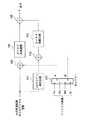
図1は、本発明の第1の実施の形態に係る信号処理装置の概略を示すブロック図である。以下、各ブロックについて説明する。
【0025】
1は、撮像手段たるCCDであり、受光された映像を電気信号に変換して蓄積し、そのアナログ信号を出力する。CCD1の受光部の表面にはカラーフィルターが設けられている。カラーフィルターには、例えば、イエロー(Ye)、シアン(Cy)、マゼンダ(Mz)およびグリーン(G)からなる補色系カラーフィルターや、レッド(R)、グリーン(G)およびブルー(B)からなる純色系カラーフィルターがあり、その配列などを組み合わせると様々な種類のCCDを使用することができる。なお、本発明の第1の実施の形態に係る信号処理装置のCCD1では、例えば、図2に示すように、第nラインの画素31、32、33および34、また、第n+2の画素39、40、41および42において、2画素周期の配列でYeとCyのカラーフィルタの色を割り当て、第n+1ラインの画素35、36、37および38、また、第n+3の画素43、44、45および46において2画素周期の配列でMzとGのカラーフィルタの色を割り当てている。すなわち、Ye、Cy、GおよびMzの色からなるカラーフィルターを割り当てた2画素周期の配列の補色系カラーフィルターを使用する。
【0026】
2は、A/D変換回路であり、CCD1からのアナログ信号を任意ビットのデジタル信号に変換する。通常、このデジタル信号は10ビット程度で出力される。
【0027】
51は、色処理系の一連の処理ブロックであり、最終的には色差信号を出力する。また、A/D変換回路2の出力するデジタル信号中の色の信号の帯域を制限する処理を施す帯域制限手段でもある。色処理系51には、3乃至7の各ブロックの処理が含まれる。
【0028】
52は、輝度処理系の一連の処理ブロックであり、最終的には輝度信号を出力する。輝度処理系52には、8乃至11の各ブロックの処理が含まれる。
【0029】
次に、色処理系51に含まれる各ブロックについて説明する。
【0030】
3は、色補間回路であり、補色系カラーフィルターの各フィルターの色のデジタル信号を組み合わせて各画素毎に補色の4色(Ye,Cy,MzおよびG)を組み合わせた色を作る補間により、補色信号を出力する。
【0031】
4は、マトリクス回路であり、補色信号をマトリクス変換して、純色の3色(R,GおよびB)とし、RGB信号を出力する。なお、カラーフィルターの分光感度特性や被写体の色温度等を考慮して、適宜、マトリクス係数を変えて最適のRGB信号を出力する。
【0032】
5は、色レベル制御手段たる色抑圧回路であり、マトリクス回路4の出力するRGB信号から低輝度部の色ノイズを除去するとともに飽和したCCD1の高輝度な色を含んだ画素の色を抑圧することができる。つまり、輝度信号の低輝度部もしくは高輝度部を検出し、その色のレベルを制御することができ、これを色抑圧という。この回路の詳細については後述するが、この回路中には、図3に示すように検出手段たる輝度レベル検値回路70が含まれている。
【0033】
6は、ガンマ補正回路であり、RGB信号について、例えば、入力10ビットの信号を8ビットで出力するガンマ補正をする。
【0034】
7は、色差マトリクス回路であり、RGB信号を色差信号R−Yおよび色差信号B−Yに変換する。
【0035】
次に、輝度処理系52に含まれる各ブロックについて説明する。
【0036】
8は、色キャリア除去回路であり、A/D変換回路2からのデジタル信号をローパスフィルター等に通して、色キャリア成分を除去して輝度信号のみを出力する。
【0037】
9は、輝度色差補正回路であり、被写体の色温度がCCD1のカラーフィルターにあらかじめ設定された色温度に比べ大きくずれている場合に輝度信号中の色成分のバランスも崩れてしまうので、これを色差信号で補正している。例えば、被写体の色温度がCCD1のカラーフィルターにあらかじめ設定された色温度に比べ低い場合に、信号処理装置により処理され再現された被写体の赤い部分の輝度成分が大きくなって忠実に、色を再現できなくなるので、これを補正する。
【0038】
10は、アパーチャー補正回路であり、受光された映像がCCD1に到達する以前の図示しない光学ローパスフィルターや色キャリヤ除去回路8のローパスフィルター等で失われた高域の信号成分を補正する。
【0039】
11は、ガンマ補正回路であり、輝度信号について、例えば、入力10ビットの信号を8ビットで出力するガンマ補正をする。TVモニター等の逆ガンマ特性を補い、画面上でリニアーな映像を映し出すための補正回路である。また、TVモニターだけでなく、プリンター出力やJPEG圧縮するため、および高画質化のためにも重要な回路ブロックである。
【0040】
ここで、色処理系51と輝度処理系52との間に位置する12は、補正用マトリクス回路であり、色処理系51の色抑圧回路5のRGB信号出力から輝度処理系52の輝度色差補正回路9で使用する輝度色差補正用の色差信号を作るための回路である。
【0041】
次に、本発明の第1の実施の形態に係る信号処理装置の色抑圧回路5について図3を参照して説明する。
【0042】
色抑圧回路5は、輝度マトリクス回路69、輝度レベル検値回路70、乗算器61乃至64、加算器65乃至67、そして減算器68から構成されている。
【0043】
輝度マトリクス回路69は、従来の信号処理装置の色抑圧回路にはなかった回路である。従来の色抑圧回路においては、図14に示すように、輝度レベル検値回路71で色ゲイン係数kを算出し、そして、入力信号である色差信号R−Yおよび色差信号B−Yのそれぞれに乗算器72および73で、色ゲイン係数kとを掛け合わせて、色差信号k(R−Y)および色差信号k(B−Y)を出力していることからも分かるように、色抑圧回路に入出力する信号が色差信号であった。しかしながら、本発明の第1の実施の形態の色抑圧回路5に入出力される信号はRGB信号であるため、RGB信号を輝度信号Yにマトリクス変換する輝度マトリクス回路69を導入している。
【0044】
本発明の第1の実施の形態の輝度レベル検値回路70は、図4に示すように、ローパスフィルター(LPF)91、コンパレーター92および93、低輝度傾き係数回路94、高輝度傾き係数回路95、リミッタ97および98、セレクタ99から構成され、色抑圧回路5の内部で、入力される輝度信号Yに応じて色ゲイン係数kを出力する。
【0045】
ローパスフィルター(LPF)91は、入力した輝度信号の帯域を制限する。このローパスフィルター(LPF)91の周波数特性は、色抑圧される色の信号の周波数帯域より広帯域か、もしくは同等となっている。色抑圧される色の信号より狭帯域の場合、色抑圧すべき色の信号だけでなくその周辺の色の信号をも抑圧してしまうためである。また、色抑圧される色の信号を、指定の画素だけでなくその周辺も含めて色抑圧する場合、ローパスフィルター(LPF)91は、対象とする画素を広げて周辺の画素の色抑圧を行う。従って、輝度部の検出のための信号の周波数帯域が色抑圧をする色差信号の周波数帯域より狭帯域とならないため、正しく飽和している画素を色抑圧することが可能となる。
【0046】
コンパレーター92は、基準値である低輝度部色ノイズ境界レベル(A)と、ローパスフィルター(LPF)91の出力である輝度信号Yのレベルとを比較する。比較した結果、輝度信号Yのレベルが低輝度部色ノイズ境界レベル(A)以上の場合、リミッタ97を制御して、色ゲイン係数kを1とする。一方、輝度信号Yのレベルが低輝度部色ノイズ境界レベル(A)以下の場合、ローパスフィルター(LPF)91の出力に低輝度部傾き係数回路94において、低輝度部側の増加直線の傾きaの係数を掛け、リミッタ97から出力する。この傾きaの係数が大きくて、輝度信号Yのレベルが低輝度部色ノイズ境界レベル(A)に到達する前に色ゲイン係数kが1を超える場合、リミッタ97を制御して色ゲイン係数を1に固定する。
【0047】
コンパレーター93は、基準値である高輝度部色抑圧境界レベル(B)とローパスフィルター(LPF)91との出力を比較する。比較した結果、輝度信号Yのレベルが高輝度部色抑圧境界レベル(B)以下の場合、セレクタ99がリミッタ97の出力側に選択され、色ゲイン係数kを1とする。一方、輝度信号Yのレベルが高輝度部色抑圧境界レベル(B)以上の場合、セレクタ99がリミッタ98の出力側に選択され、ローパスフィルター(LPF)91の出力に、高輝度部傾き係数回路95で係数−bを掛けた信号とkに相当するオフセット値を加算し、傾き−bの係数と加算器100により、高輝度部側の減少直線を実現している。なお、リミッタ98は、出力が負にならないようにしている。
【0048】
従って、輝度レベル検値回路70は、輝度信号Yのレベルから色ゲイン係数kを出力することができるが、その関係は図5に示すようになる。
【0049】
輝度レベル検値回路70は、低輝度部色ノイズ境界レベル(A)までは、輝度信号のレベルが上昇すると色ゲイン係数kを直線的な傾きaの軌跡で増加させて算出し、低輝度部色のノイズを除去している。また、輝度レベル検値回路70は、低輝度部色ノイズ境界レベル(A)より、輝度信号のレベルが上昇すると色ゲイン係数kを一定の1にして算出するが、高輝度部色抑圧境界レベル(B)以上の輝度信号のレベルでは、輝度信号のレベルの上昇とともに色ゲイン係数kを直線的な傾き−bの軌跡で減少させて算出し、高輝度部の色を抑圧している。
【0050】
次に、上記色抑圧回路5の動作について、図3を参照して説明する。
【0051】
上述したように色抑圧回路5に入力される信号はRGB信号であり、輝度マトリクス回路69において、RGB信号を以下の式に導かれるマトリクス変換により輝度信号Yに変換し、色抑圧することができる。
【0052】
【数1】
【0053】
【数2】
【0054】
【数3】
R=Y+k(R−Y)=kR+(Y−kY) …(4)
G=Y+k(G−Y)=kG+(Y−kY) …(5)
B=Y+k(B−Y)=kB+(Y−kY) …(6)
となる。
【0055】
そこで、色抑圧回路5においては、図3に示すように、先ず、上述した輝度レベル検値回路70において、輝度信号Yから色差信号を色抑圧するための係数である0から1の色ゲイン係数kが算出される。また、入力信号であるRGB信号のR信号、G信号およびB信号のそれぞれは、乗算器61、62および63で、算出された色ゲイン係数kと掛け合わせられる。一方、輝度マトリクス回路69において、入力信号であるRGB信号のR信号、G信号およびB信号からマトリクス変換された輝度信号Yは、乗算器64で色ゲイン係数kと掛け合わされ、減算器68でもとの輝度信号Yから減算され(Y−kY)の出力を得る。従って、上述したようにk倍されたR信号、G信号およびB信号に、(Y−kY)の出力を加算器65、66および67で加えて、色抑圧したRGB信号とする。すなわち、上述した4式、5式および6式の最右辺が出力される。これらの色抑圧したRGB信号は、色ゲイン係数kが0に近づくにつれ、もとのRGB信号のレベルが減少して色が抑圧され、反対に色ゲイン係数kが1の場合は、もとのRGB信号のみになる。そこで、色抑圧回路5は、入力されるRGB信号の低輝度部の色のノイズを除去するとともに飽和したCCD1の高輝度な色を含んだ画素の色を抑圧することが可能となる。
【0056】
次に、本発明の第1の実施の形態に係る信号処理装置の信号処理の作用について、図1を参照して説明する。
【0057】
受光された被写体像の映像は、CCD1で電気信号に変換され、A/D変換回路2においてアナログ信号からデジタル信号に変換される。変換されたデジタル信号は、色処理系51と輝度信号系52に分かれて処理されることになる。
【0058】
色処理系51では、A/D変換回路2の出力するデジタル信号が色補間回路3において、CCD1の各画素についてイエロー(Ye)、シアン(Cy)、マゼンダ(Mz)およびグリーン(G)からなる4色の補色信号で出力される。補色信号は、マトリクス回路4で、レッド(R)、グリーン(G)およびブルー(B)からなる純色に変換され、RGB信号として出力される。次に、色抑圧回路5において、輝度処理系52の色キャリヤ除去回路8の輝度信号のレベルから低輝度部もしくは高輝度部を検出し、RGB信号が低輝度部の色のノイズを除去されるとともに飽和したCCD1の高輝度な色を含んだ画素の色を抑圧される。そして、ガンマ補正回路6において、TVモニター等に映し出すための映像信号にマッチングされ、色差マトリクス回路7で色差信号に変換され出力される。
【0059】
また、色補間回路3等の色処理系51の一連の処理により色の信号の帯域が制限される。つまり、A/D変換回路2の出力するデジタル信号中の色の信号は、色処理系51により帯域を制限される処理を施され、色差信号に変換されている。
【0060】
一方、輝度処理系52では、A/D変換回路2の出力するデジタル信号が色キャリヤ除去回路8において、色キャリア成分が除去され、ほぼ無加工の輝度信号となる。次に、輝度信号は、輝度色差補正回路9において、輝度信号中の色成分のバランスを輝度色差補正用の色差信号で補正される。この輝度色差補正用の色差信号は、色抑圧回路5により処理されたRGB信号出力から補正用マトリクス回路12のマトリクス変換によって作られた色差信号である。次に、輝度信号は、アパーチャー補正回路10で高域部の特性が持ち上げられる。さらに、ガンマ補正回路11において、色処理系51と同様に、ガンマ補正され、最終的な輝度信号が出力される。
【0061】
上述のように、本発明の第1の実施の形態では、輝度処理系52のアパーチャー補正回路10やガンマ補正回路11の処理の前に、RGB信号を色抑圧回路5で色抑圧する処理をすることが可能となり、従来の信号処理装置に比べて色処理系の帯域制限処理が少なくなる。
【0062】
従って、CCD1の飽和した画素の影響が周囲に広がってしまうことが少なくなり、TVモニター等で被写体像を再現する際に、最終出力画像の高輝度部のみならず、高輝度部の周辺までが被写体と異なる偽色によって、画質の劣化を生じる場合も少なくなる。
【0063】
(実施の形態2)
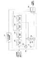
図6は、本発明の第2の実施の形態に係る信号処理装置の概略を示すブロック図である。
【0064】
本発明の第2の実施の形態に係る信号処理装置では、CCD1、A/D変換回路2、色補間回路3、マトリクス回路4、ガンマ補正回路6、色差マトリクス回路7、色キャリヤ除去回路8、輝度色差補正回路9、アパーチャー補正回路10、ガンマ補正回路11および補正用色差マトリクス回路12の各ブロックは、第1の実施の形態に係る信号処理装置と同じであるが、色レベル制御手段たる色抑圧回路13は、上述の本発明の第1の実施の形態と異なり、輝度信号の低輝度部もしくは高輝度部を検出し、色補間回路3の出力する補色に対し、マトリクス回路4の前で各色のレベルを制御して色抑圧を行うことができる点に特徴がある。つまり、本発明の第1の実施の形態に係る信号処理装置では、色処理系51の中の色抑圧回路5は、マトリクス回路4からのRGB信号を処理してガンマ補正回路6へ出力しているのに対し、本発明の第2の実施の形態に係る信号処理装置では、色処理系51の中の色抑圧回路13は、色補間回路3からの補色信号を処理し、マトリクス回路4へ出力しており、この処理手順が第1の実施の形態と異なっており、その他は本発明の実施の形態に係る信号処理と同じである。従って、ここでは特に色抑圧回路13について、図7を参照して説明する。
【0065】
上記色抑圧回路13は、輝度マトリクス回路91、輝度レベル検値回路70、乗算器81乃至85、加算器86乃至89、そして減算器90から構成されている。
【0066】
輝度マトリクス回路91は、色抑圧回路13において、入出力される信号が補色信号であり、この補色信号を輝度信号Yにマトリクス変換するために導入されている。
【0067】
また、輝度レベル検値回路70は、上述した本発明の第1の実施の形態と同じ回路である。
【0068】
次に、上記色抑圧回路13の動作について、図7を参照して説明する。
【0069】
上述したように色抑圧回路13に入力される信号は補色信号であり、輝度マトリクス回路91において、補色信号を以下の式に導かれるマトリクス変換により輝度信号Yに変換し、色抑圧することができる。
【0070】
【数4】
【0071】
【数5】
【0072】
【数6】
Cy=m11[Y+k(R−Y)]+m12[Y+k(G−Y)]+m13[Y+k(B−Y)]=(m11+m12+m13)Y−(m11+m12+m13)kY+k(m11R+m12G+m13B)=(m11+m12+m13)(Y−kY)+kCy
ここで、(m11+m12+m13)は成分比の合計なので1となる。従って、
Cy=(Y−kY)+kCy …(10)
となり、同様にYe,G,Mzについても、
Ye=(Y−kY)+kYe …(11)
G =(Y−kY)+kG …(12)
Mz=(Y−kY)+kMz …(13)
となる。
【0073】
そこで、色抑圧回路13においては、図7に示すように、第1の実施の形態と同様に、先ず、輝度レベル検値回路70において、輝度信号Yから色差信号を色抑圧するための係数である0から1の色ゲイン係数kが算出される。また、入力信号である補色信号のCy信号、Ye信号、Mz信号およびG信号のそれぞれは、乗算器81乃至84で、算出された色ゲイン係数kと掛け合わせられる。一方、輝度マトリクス回路91において、入力信号である補色信号のCy信号、Ye信号、Mz信号およびG信号から変換された輝度信号Yは、乗算器85で色ゲイン係数kと掛け合わされ、減算器90でもとの輝度信号Yから減算され(Y−kY)の出力を得る。従って、上述したようにk倍されたCy信号、Ye信号、Mz信号およびG信号に、(Y−kY)の出力を加算器86乃至89で加えて、色抑圧された補色信号とする。すなわち、上述した10式乃至13の右辺が出力される。これらの色抑圧された補色信号は、色ゲイン係数kが0に近づくにつれ、もとの補色信号のレベルが減少して色が抑圧され、反対に色ゲイン係数kが1の場合は、もとの補色信号のみになる。そこで、色抑圧回路13は、入力される補色信号の低輝度部の色のノイズを除去するとともに飽和したCCD1の高輝度な色を含んだ画素の色を抑圧することが可能となる。
【0074】
次に、本発明の第2の実施の形態に係る信号処理装置の信号処理の作用について図6を参照して説明するが、ここでは特に第1の実施の形態と異なる点について説明する。
【0075】
色処理系51では、色補間回路3においてCCD1の各画素について補色信号が出力される。本発明の第2の実施の形態の色抑圧回路13では、補色信号が色抑圧され、色抑圧された補色信号は、マトリクス回路4で純色のRGB信号に変換され、以後、本発明の第1の実施の形態と同様に処理されて、色差信号が出力される。
【0076】
また、輝度処理系52でも、本発明の第1の実施の形態と同様に処理され輝度信号が出力されるが、本発明の第2の実施の形態の色抑圧回路13の出力が補色信号であるので、マトリクス回路4において変換されたRGB信号から、補正用マトリクス回路12でマトリクス変換した色差信号を用いて、輝度色差補正している。
【0077】
上述のように、本発明の第2の実施の形態では、色処理系51の中で色抑圧回路13が色補間回路3からの補色信号を処理し、マトリクス回路4へ出力しているため、本発明の第1の実施の形態における色抑圧する領域よりもその領域を広げる必要がない。つまり、色処理系の早い段階に色抑圧する処理をするので、不必要に色抑圧する領域を広げることなく、低輝度部の色のノイズを除去し、飽和したCCDの画素の色を抑圧することができる。
【0078】
従って、本発明の第1の実施の形態の信号処理装置よりもCCD1の飽和した画素の影響が周囲に広がってしまうことが少なくなり、TVモニター等で被写体像を再現する際に、最終出力画像の高輝度部のみならず、高輝度部の周辺までが被写体と異なる偽色によって、画質の劣化を生じる場合も少なくなる。
【0079】
(実施の形態3)
図8は、本発明の第3の実施の形態の信号処理装置の概略を示すブロック図である。
【0080】
本発明の第3の実施の形態に係る信号処理装置では、CCD1、A/D変換回路2、色補間回路3、マトリクス回路4、ガンマ補正回路6、色差マトリクス回路7、色キャリヤ除去回路8、輝度色差補正回路9、アパーチャー補正回路10、ガンマ補正回路11および補正用色差マトリクス回路12の各ブロックは、第1の実施の形態に係る信号処理装置と同じであるが、色レベル制御手段たる色抑圧回路21は、上述の本発明の実施の形態と異なり、帯域制限手段たる色処理系51の色補間回路3等の一連の処理により色の信号が帯域制限される前に、輝度信号の低輝度部もしくは高輝度部を検出し、A/D変換回路2の出力するデジタル信号の色のレベルを制御することができる点に特徴がある。従って、ここでは特に色抑圧回路21について、図9を参照して詳細に説明する。
【0081】
上記色抑圧回路21は、図9に示すように、検出手段たるCCD出力飽和検値回路121、ディレイ回路122、輝度信号発生回路123、乗算器124および125、減算器126、そして加算器127とを有しており、低輝度部の色のノイズを除去するとともに飽和したCCD1の高輝度な色を含んだ画素の色を抑圧する回路である。色抑圧回路21は、A/D変換回路の出力するデジタル信号を入力信号として処理しており、このデジタル信号は、色の情報を時系列的に含んでいる。
【0082】
また、入力信号がA/D変換回路の出力するデジタル信号であることから、色抑圧回路21には、図7に示すような第2の実施の形態の色抑圧回路13の4つの乗算器81乃至84は必要なく、同じ役割をする1つの乗算器124で十分である。
【0083】
CCD出力飽和検値回路121は、上述した本発明の第1の実施の形態の輝度レベル検値回路70と同等の回路であり、入力信号のレベルに応じて、色抑圧係数k1を出力する。すなわち、CCD出力飽和検値回路121において、A/D変換回路2の出力するデジタル信号のCCD1の画素の中から指定した画素の色のレベルに合わせて色抑圧係数k1を算出し、出力する。
【0084】
CCD出力飽和検値回路121において、図5に示す輝度信号Yのレベル(横軸)と色ゲイン係数k(縦軸)との上述した関係のように、低輝度部側では入力デジタル信号のレベルの上昇に合わせて色抑圧係数k1が大きくなり、高輝度部側では入力デジタル信号のレベルの上昇に合わせて色抑圧係数k1が小さくなる。従って、低輝度部側の色のノイズを除去するとともに飽和したCCD1の高輝度な色を含んだ画素の色を抑圧する色抑圧を同一の回路で行うことができる。
【0085】
また、ディレイ回路122は、A/D変換回路2の出力するデジタル信号をCCD出力飽和検値回路121の出力のタイミングに合わせて、時間を遅れさせる回路である。通常、フリップフロップ等が用いられている。
【0086】
次に、輝度信号発生回路123は、CCD1の画素の中から指定した画素と、その周囲の画素から輝度信号Yを作り出す回路である。つまり、この輝度信号Yは、CCD出力飽和検値回路121で飽和を検値したCCD1の画素とその周囲の画素から輝度信号Yを作り出した場合、色抑圧が必要となる。例えば、図2に示すようなカラーフィルター配列のCCDにおいて、Yeのカラーフィルターを持つ画素41が飽和した場合、画素41の飽和の影響を受ける輝度信号は、画素36,37,40および41からなる輝度信号Y1と、画素37,38,41および42からなる輝度信号Y2と、画素40,41,44および45からなる輝度信号Y3と、画素41,42,45および46からなる輝度信号Y4の4つであり、この画素36,37,38,40,41,42,44,45および46に対して同一の色抑圧係数k1を掛けて色抑圧する必要がある。
【0087】
輝度信号発生回路123は、図10に示すように、1水平ラインデータ遅延回路131、乗算器132および133、ホールド加算回路134および135、加算器136、そして、セレクター137を有している。
【0088】
1水平ラインデータ遅延回路131は、A/D変換回路2の出力するデジタル信号の中で、CCD1の1水平ライン分の画素データを遅らせることができ、SRAM等にCCD1の1水平ライン分の画素データを記憶して、読み出す回路等で構成されている。
【0089】
セレクター137は、A/D変換回路2の出力するデジタル信号が色の情報を時系列的に含んでいるため、乗算器132および133で乗算する場合の色の情報、つまり補色のYe,Cy,GおよびMzのどれか一つに合わせて、RGBに変換するためのマトリクス係数を適宜最適になるように選択し、後述する式(14)のマトリクス係数によりA/D変換回路2の出力するデジタル信号を輝度信号Yに変換するための回路である。
【0090】
また、乗算器132および133は、図2に示すように水平方向に隣り合ったCCD1の画素のデータを乗算しており、ホールド加算回路134および135は、これらのデータを重み付けし、加算器136は、ホールド加算回路134からの信号とホールド加算回路135からの信号とを加えている。
【0091】
従って、輝度信号発生回路123は、色の情報を時系列的に含んでいるA/D変換回路からのデジタル信号を、RGB信号に変換し、その後、次の式(14)に示されるように変換し、輝度信号Yを出力する動作をする。
【0092】
【数7】
【0093】
ディレイ回路122からタイミングを合わせて出力されたデジタル信号は、CCD出力飽和検値回路121において、算出された色抑圧係数k1を乗算器124で乗算される。また、輝度信号回路において発生した輝度信号Yは、色抑圧係数k1を乗算器125で乗算し、減算器126においてもとの輝度信号Yから減算されることから、(Y−k1Y)が出力される。従って、加算器127において演算結果が求まり、時系列的に色抑圧されたデジタル信号が出力される。
【0094】
色抑圧したデジタル信号は、色抑圧係数k1が0に近づくにつれ、もとのデジタル信号のレベルが減少して色が抑圧され、反対に色抑圧係数k1が1の場合は、もとのデジタル信号のみになる。すなわち、デジタル信号の低輝度部の色のノイズを除去するとともに飽和したCCD1の高輝度な色を含んだ画素の色を抑圧することが可能となる。
【0095】
次に、本発明の第3の実施の形態に係る信号処理装置の信号処理の作用について図8を参照して説明するが、ここでは特に第1の実施の形態と異なる点について説明する。
【0096】
色処理系51では、初めに、A/D変換回路2のの出力するデジタル信号が、色抑圧回路21により色抑圧され、色補間回路3において、CCD1の各画素についてイエロー(Ye)、シアン(Cy)、マゼンダ(Mz)およびグリーン(G)からなる4色の補色信号で出力される。補色信号は、マトリクス回路4で、レッド(R)、グリーン(G)およびブルー(B)からなる純色に変換され、RGB信号として出力される。次に、ガンマ補正回路6、色差マトリクス回路7で処理が行なわれて、色差信号R−Yおよび色差信号B−Yとなり出力される。
【0097】
一方、輝度処理系52では、本発明の第1の実施の形態のように、マトリクス回路4からのRGB信号から、補正用マトリクス回路12で輝度色差補正信号を作り、色キャリア除去後の輝度信号に対して輝度色差補正を行い、その後アパーチャー補正とガンマ補正とをし、輝度信号を出力する。また、上述した色抑圧回路21の回路中に輝度信号発生回路123があるため、色キャリヤ除去回路8の出力である輝度信号が色抑圧回路21へ入力されていない。
【0098】
上述のように、本発明の第3の実施の形態では、A/D変換回路2の出力するデジタル信号により色抑圧している。色抑圧する処理を色処理系の初期段階で行うことにより、色処理系の一連の処理による帯域制限の影響を受ける前に色抑圧処理をすることができるので、飽和したCCDの画素の影響が周囲に広がることはなく、TVモニター等で被写体像を再現する際に、高画質な画像を得る正しい色処理をすることができる。
【0099】
(実施の形態4)
本発明の第4の実施の形態に係る信号処理装置では、本発明の第3の実施の形態で述べた図8に示す色抑圧回路21の代わりに、色補正回路を用いる場合について説明する。つまり、色抑圧係数k1を掛けて色抑圧するのでなく、CCDの画素の飽和を検出した場合、飽和した画素の周囲の画素から補間することにより飽和画素を補正する。
【0100】
従って、色補正回路の他のブロックの処理は、第3の実施の形態と同じであり、色補正回路について、以下説明することとする。
【0101】
色補正回路の補間には、1次元および2次元のリニアー補間、または、補間するための画素の領域を広げて、ローパスフィルターの特性により補間等を行う場合がある。
【0102】
先ず、1次元のリニアー補間を行う場合について説明する。
【0103】
図11は、1次元のリニアー補間で色補正するのための色補正回路であり、CCD出力飽和検出回路141、補間回路142およびセレクター143から構成されている。
【0104】
CCD出力飽和検出回路141は、A/D変換回路2の出力するデジタル信号の出力が飽和している場合に1を出力し、飽和していない場合に0を出力する。
【0105】
補間回路142は、CCDに飽和した画素がある場合、飽和したCCDの画素の周囲にある同色の画素から飽和した画素を補うための回路であり、1次元のリニアー補間を用いた場合を示している。
【0106】
セレクター143は、CCD出力飽和検出回路141の出力により切り替えられる。通常、A/D変換回路2の出力するデジタル信号がそのまま出力されるように選択されているが、CCDに飽和した画素がある場合、セレクターが切り替わり、補間回路142から飽和した画素の補間されたデジタル信号が出力される。
【0107】
ここで、補間回路142は、CCD1の同色の画素の間隔分の遅延量のディレイ回路144および147と、加算器145と、1/2回路146とを有している。また、1/2回路146は、具体的にはデータをローサイドバンド(LSB)側に1ビットシフトする働きをする。従って、CCDの画素の飽和を検出した場合、飽和した画素の周囲の画素の信号を使用できるようになる。
【0108】
次に、補間用の画素の周囲領域を広げてローパスフィルター特性の補間を行う場合について説明する。
【0109】
補間用の画素の周囲領域を広げてローパスフィルター特性の補間を行う場合、1次元のリニアー補間で色補正するのための補間回路142とは、補間回路158が、図12に示すように、ディレイ回路154、155、156、および157の4つを用い、係数回路151および152、そして加算器153、159および160から構成される点で異なっている。ここで、補間回路158の補間動作は、A/D変換回路2の出力するデジタル信号の入力とディレイ回路157の出力を加算器159で加算し、ディレイ回路154とディレイ回路156の出力を加算器160で加算して、それぞれ係数回路151および152で所定の係数を乗算し、加算器153でそれぞれを加算することによる。つまり、補間回路158は、係数回路151および152の係数によりフィルター特性が定まるデジタルフィルターを構成している。なお、補間回路158以外は、図11に示す1次元のリニアー補間を用いた場合と同じである。
【0110】
上述のように、本発明の第4の実施の形態では、CCDに飽和した画素がある場合、色抑圧する代わりに、飽和したCCDの画素の周囲にある同色の画素から飽和した画素を補う処理をすることにより、色抑圧回路よりもゲート規模の小さい回路とすることができる。
【0111】
また、本発明の第4の実施の形態では、本発明の第3の実施の形態の信号処理装置と同様に、色補正回路による処理を色処理系の初期段階で行うことにより、色処理系の一連の処理による帯域制限の影響を受けることがない。そこで、飽和したCCDの画素の影響が周囲に広がることはなく、TVモニター等で被写体像を再現する際に、高画質な画像を得る正しい色処理をすることができる。
【0112】
また、人の顔等の被写体像の場合、頭部や鼻の光を反射している高輝度部は、色抑圧よりも補間回路で処理した方がより自然な画像を再現することができる。
【0113】
【発明の効果】
上述したように、本発明によれば、色度処理系のアパーチャー補正やガンマ補正の前に、RGB信号、補正信号、デジタル信号を色抑圧回路で処理することにより、従来の信号処理装置と比較して、色信号の低輝度部の色のノイズを除去するとともに飽和している高輝度な色を含んだ画素を正しく色抑圧することができるので、飽和したCCDの画素の影響が周囲に広がることはなく、TVモニター等で被写体像を再現する際に、高画質な画像を得る正しい色処理をすることができる。
【0114】
デジタル信号を色補正回路で処理することにより、さらに、自然な画像を再現することができる。
【図面の簡単な説明】
【図1】本発明の第1の実施の形態に係る信号処理装置の概略の構成を示すブロック図である。
【図2】本発明の第1の実施の形態のCCDの補色のカラーフィルターを説明するための図である。
【図3】本発明の第1の実施の形態の色抑圧回路について説明するための図である。
【図4】本発明の第1の実施の形態の輝度レベル検値回路について説明するための図である。
【図5】本発明の第1の実施の形態の輝度レベル検値回路の輝度信号Yのレベルから色ゲイン係数kを出力する関係について説明するための図である。
【図6】本発明の第2の実施の形態に係る信号処理装置の概略の構成を示すブロック図である。
【図7】本発明の第2の実施の形態の色抑圧回路について説明するための図である。
【図8】本発明の第3の実施の形態に係る信号処理装置の概略の構成を示すブロック図である。
【図9】本発明の第3の実施の形態の色抑圧回路について説明するための図である。
【図10】本発明の第3の実施の形態の輝度信号発生回路について説明するための図である。
【図11】本発明の第4の実施の形態の色補正回路について、1次元のリニアー補間を用いた場合を説明するための図である。
【図12】本発明の第4の実施の形態の色補正回路について、補間用の画素の周囲領域を広げてローパスフィルター特性の補間を行う場合を説明するための図である。
【図13】従来の信号処理装置の概略の構成を示すブロック図である。
【図14】従来の色抑圧回路について説明するための図である。
【符号の説明】
1 CCD
2 A/D変換回路
3 色補間回路
4 マトリクス回路
5、13、20、21 色抑圧回路
6、11 ガンマ補正回路
7 色差マトリクス回路
8 色キャリヤ除去回路
9 輝度色差補正回路
10 アパーチャー補正回路
12 補正用マトリクス回路
69 輝度マトリクス回路
70、71 輝度レベル検値回路
91 ローパスフィルター
94 低輝度部傾き係数回路
95 高輝度部傾き係数回路
97、98 リミッタ
99、137 セレクター
121 CCD出力飽和検値回路
122 ディレイ回路
123 輝度信号発生回路
131 1水平ライン遅延回路
141 CCD出力飽和検出回路
144、147、154、155、156、157 ディレイ回路[0001]
BACKGROUND OF THE INVENTION
The present invention relates to an imaging output signal processing apparatus and an imaging signal processing method for converting a subject image into an image signal and processing it into a luminance signal and a color difference signal.
[0002]
[Prior art]
Conventionally, an imaging output signal processing apparatus that converts a subject image into an image signal and processes it into a luminance signal and a color difference signal performs processing according to a signal processing block as shown in FIG.
[0003]
The received image of the subject image is converted into an electrical signal by the
[0004]
In the
[0005]
Further, the band of the color signal is limited by a series of processes of the
[0006]
On the other hand, in the
[0007]
[Problems to be solved by the invention]
Conventionally, the
[0008]
However, when the pixel of the
[0009]
Further, since color suppression processing is performed at the final stage of the
[0010]
On the other hand, when the above-described color suppression is performed, the color information of the final output video is lost due to the suppression even around the subject, which may cause deterioration in image quality.
[0011]
Further, the frequency band of the signal for detecting the saturated high luminance portion of the
[0012]
The present invention has been made in view of the above circumstances, and the present invention reduces the influence of the color signal being band-limited by the color processing system, and enables signal processing to obtain a non-degraded image. An object is to provide an apparatus and a signal processing method for imaging.
[0013]
[Means for Solving the Problems]
In order to solve the above problems, a signal processing apparatus according to a first aspect of the present invention is a signal processing apparatus for converting a subject image into an image signal and processing the image signal into a luminance signal and a color difference signal. Imaging means for converting and storing the image signal into the image signal, detection means for detecting a low-luminance portion or a high-luminance portion of the image signal accumulated by the imaging means, and a low-luminance portion detected by the detection means or Color level control means for controlling the level of the color signal of the high-luminance portion, and color interpolation processing of the color signal of the image signal to limit the band, gamma correction of the color signal of the band limited, Color processing means for processing the signal of the color subjected to gamma correction into a color difference signal, and the detection means uses the color level control unit as an image signal for detecting the low luminance part or the high luminance part. Hirotai than the frequency band of the color signal is controlled byRegional A luminance signal having a frequency band is used, and the color level control unit is configured to use the high luminance part or the low luminance of the color signal before the color signal in the processing path of the color processing unit is gamma corrected. Control is performed so as to suppress the color gain of the portion.
[0014]
Preferably, in
[0015]
Preferably, the
[0016]
Also preferably, the
[0018]
In order to solve the above-described problem, an imaging signal processing method according to a fifth aspect of the present invention is an imaging signal processing method for converting a subject image into an image signal and processing the image signal into a luminance signal and a color difference signal. A detection step for detecting a low-luminance portion or a high-luminance portion of the image signal; a color level control step for controlling a color signal level of the low-luminance portion or the high-luminance portion detected by the detection step; and the image A color processing step of limiting a band by performing color interpolation processing on a signal color signal, performing gamma correction on the signal of the color whose band is limited, and processing the signal of the color subjected to gamma correction into the color difference signal; And the detecting step is wider than the frequency band of the color signal controlled by the color level control step as an image signal for detecting the low luminance portion or the high luminance portion.Regional A luminance signal having a frequency band is used, and the color level control step is executed before gamma correction of the color signal in the color processing step, and the color signal of the high luminance portion or the low luminance portion of the color signal is executed. Control is performed to suppress the color gain.
[0019]
Preferably, in claim 5, the color level control step controls the level of the color signal before the band of the color signal is limited. It is characterized by.
[0020]
Preferably, the claim5 The color level control step is characterized in that the color level is color-suppressed in accordance with the detected color signal.
[0021]
Also preferably, the claims5 The color level control step performs color interpolation according to the detected color signal.
[0023]
DETAILED DESCRIPTION OF THE INVENTION
Hereinafter, embodiments of the present invention will be described in detail with reference to the drawings.
[0024]
(Embodiment 1)
FIG. 1 is a block diagram showing an outline of a signal processing apparatus according to the first embodiment of the present invention. Hereinafter, each block will be described.
[0025]
[0026]
[0027]
51 is a series of processing blocks of the color processing system, and finally outputs a color difference signal. Further, it is also a band limiting means for performing processing for limiting the band of the color signal in the digital signal output from the A /
[0028]
52 is a series of processing blocks of the luminance processing system, and finally outputs a luminance signal. The
[0029]
Next, each block included in the
[0030]
3 is a color interpolation circuit, which combines the digital signals of the colors of the respective filters of the complementary color system color filter to interpolate colors that combine four complementary colors (Ye, Cy, Mz, and G) for each pixel, Outputs complementary color signals.
[0031]
[0032]
Reference numeral 5 denotes a color suppression circuit as color level control means, which removes the color noise of the low luminance part from the RGB signal output from the
[0033]
[0034]
[0035]
Next, each block included in the
[0036]
A color
[0037]
[0038]
[0039]
[0040]
Here, 12 positioned between the
[0041]
Next, the color suppression circuit 5 of the signal processing apparatus according to the first embodiment of the present invention will be described with reference to FIG.
[0042]
The color suppression circuit 5 includes a
[0043]
The
[0044]
As shown in FIG. 4, the luminance
[0045]
The low pass filter (LPF) 91 limits the band of the input luminance signal. The frequency characteristic of the low-pass filter (LPF) 91 is wider than or equal to the frequency band of the color signal to be color-suppressed. This is because, when the band is narrower than the color-suppressed color signal, not only the color signal to be color-suppressed but also the surrounding color signals are suppressed. Further, when the color signal to be color-suppressed includes not only the designated pixel but also its periphery, the low-pass filter (LPF) 91 widens the target pixel and performs color suppression on the peripheral pixels. . Therefore, since the frequency band of the signal for detecting the luminance part is not narrower than the frequency band of the color difference signal for color suppression, it is possible to suppress the color of pixels that are correctly saturated.
[0046]
The
[0047]
The
[0048]
Therefore, the luminance
[0049]
The luminance
[0050]
Next, the operation of the color suppression circuit 5 will be described with reference to FIG.
[0051]
As described above, the signal input to the color suppression circuit 5 is an RGB signal. In the
[0052]
[Expression 1]
[0053]
[Expression 2]
[0054]
[Equation 3]
R = Y + k (R−Y) = kR + (Y−kY) (4)
G = Y + k (G−Y) = kG + (Y−kY) (5)
B = Y + k (B−Y) = kB + (Y−kY) (6)
It becomes.
[0055]
Therefore, in the color suppression circuit 5, as shown in FIG. 3, first, in the above-described luminance
[0056]
Next, the operation of the signal processing of the signal processing apparatus according to the first embodiment of the present invention will be described with reference to FIG.
[0057]
The received image of the subject image is converted into an electrical signal by the
[0058]
In the
[0059]
Further, the band of the color signal is limited by a series of processes of the
[0060]
On the other hand, in the
[0061]
As described above, in the first embodiment of the present invention, before the processing of the
[0062]
Therefore, the influence of the saturated pixels of the
[0063]
(Embodiment 2)
FIG. 6 is a block diagram showing an outline of a signal processing apparatus according to the second embodiment of the present invention.
[0064]
In the signal processing apparatus according to the second embodiment of the present invention, the
[0065]
The
[0066]
The
[0067]
The luminance
[0068]
Next, the operation of the
[0069]
As described above, the signal input to the
[0070]
[Expression 4]
[0071]
[Equation 5]
[0072]
[Formula 6]
Cy = m11 [Y + k (R−Y)] + m12 [Y + k (G−Y)] + m13 [Y + k (B−Y)] = (m11 + m12 + m13) Y− (m11 + m12 + m13) kY + k (m11R + m12G + m13B) = (m11 + m12 + m13) (Y−kY) ) + KCy
Here, (m11 + m12 + m13) is 1 because it is the sum of the component ratios. Therefore,
Cy = (Y−kY) + kCy (10)
Similarly, for Ye, G, and Mz,
Ye = (Y−kY) + kYe (11)
G = (Y−kY) + kG (12)
Mz = (Y−kY) + kMz (13)
It becomes.
[0073]
Therefore, in the
[0074]
Next, the operation of the signal processing of the signal processing apparatus according to the second embodiment of the present invention will be described with reference to FIG. 6, and here, in particular, points different from the first embodiment will be described.
[0075]
In the
[0076]
The
[0077]
As described above, in the second embodiment of the present invention, the
[0078]
Accordingly, the influence of the saturated pixel of the
[0079]
(Embodiment 3)
FIG. 8 is a block diagram showing an outline of a signal processing apparatus according to the third embodiment of the present invention.
[0080]
In the signal processing apparatus according to the third embodiment of the present invention, the
[0081]
As shown in FIG. 9, the
[0082]
Since the input signal is a digital signal output from the A / D conversion circuit, the
[0083]
The CCD output
[0084]
In the CCD output
[0085]
The
[0086]
Next, the luminance
[0087]
As shown in FIG. 10, the luminance
[0088]
The one horizontal line
[0089]
Since the digital signal output from the A /
[0090]
Further, as shown in FIG. 2, the
[0091]
Therefore, the luminance
[0092]
[Expression 7]
[0093]
The digital signal output in time from the
[0094]
As the color suppression coefficient k1 approaches 0, the color-suppressed digital signal has its original digital signal level reduced to suppress the color. On the contrary, when the color suppression coefficient k1 is 1, the original digital signal Become only. That is, it is possible to remove the color noise of the low luminance part of the digital signal and suppress the color of the pixel including the saturated high luminance color of the
[0095]
Next, the operation of the signal processing of the signal processing apparatus according to the third embodiment of the present invention will be described with reference to FIG. 8, and here, in particular, the differences from the first embodiment will be described.
[0096]
In the
[0097]
On the other hand, in the
[0098]
As described above, in the third embodiment of the present invention, color suppression is performed by the digital signal output from the A /
[0099]
(Embodiment 4)
In the signal processing apparatus according to the fourth embodiment of the present invention, a case will be described in which a color correction circuit is used instead of the
[0100]
Accordingly, the processing of the other blocks in the color correction circuit is the same as that in the third embodiment, and the color correction circuit will be described below.
[0101]
In the interpolation of the color correction circuit, there is a case where one-dimensional and two-dimensional linear interpolation, or an area of a pixel to be interpolated is expanded and interpolation or the like is performed according to the characteristics of the low-pass filter.
[0102]
First, a case where one-dimensional linear interpolation is performed will be described.
[0103]
FIG. 11 shows a color correction circuit for performing color correction by one-dimensional linear interpolation, and includes a CCD output
[0104]
The CCD output
[0105]
The
[0106]
The
[0107]
Here, the
[0108]
Next, a case where the surrounding area of the interpolation pixel is expanded to perform the low-pass filter characteristic interpolation will be described.
[0109]
When performing interpolation with low-pass filter characteristics by expanding the surrounding area of the pixel for interpolation, the
[0110]
As described above, in the fourth embodiment of the present invention, when there is a saturated pixel in the CCD, a process for compensating for a saturated pixel from pixels of the same color around the saturated CCD pixel instead of performing color suppression. By doing this, a circuit having a smaller gate scale than the color suppression circuit can be obtained.
[0111]
Further, in the fourth embodiment of the present invention, similarly to the signal processing apparatus of the third embodiment of the present invention, the processing by the color correction circuit is performed at the initial stage of the color processing system, thereby the color processing system. It is not affected by the bandwidth limitation by the series of processes. Therefore, the influence of the saturated CCD pixel does not spread to the surroundings, and correct color processing for obtaining a high-quality image can be performed when the subject image is reproduced on a TV monitor or the like.
[0112]
In the case of a subject image such as a human face, a high-intensity part reflecting light from the head or nose can reproduce a natural image by processing with an interpolation circuit rather than color suppression.
[0113]
【The invention's effect】
As described above, according to the present invention, before the aperture correction and the gamma correction of the chromaticity processing system, the RGB signal, the correction signal, and the digital signal are processed by the color suppression circuit, thereby comparing with the conventional signal processing apparatus. do it,Removes color noise in the low-brightness part of the color signal and correctly suppresses pixels that contain saturated high-brightness colors Therefore, the influence of the saturated CCD pixel does not spread to the surroundings, and correct color processing for obtaining a high-quality image can be performed when the subject image is reproduced on a TV monitor or the like.
[0114]
By processing the digital signal with the color correction circuit, a more natural image can be reproduced.
[Brief description of the drawings]
FIG. 1 is a block diagram showing a schematic configuration of a signal processing apparatus according to a first embodiment of the present invention.
FIG. 2 is a diagram for explaining a complementary color filter of the CCD according to the first embodiment of the present invention;
FIG. 3 is a diagram for explaining a color suppression circuit according to the first embodiment of this invention;
FIG. 4 is a diagram for explaining a luminance level detection circuit according to the first embodiment of the present invention;
FIG. 5 is a diagram for explaining a relationship of outputting a color gain coefficient k from the level of the luminance signal Y of the luminance level detection circuit according to the first embodiment of the present invention.
FIG. 6 is a block diagram showing a schematic configuration of a signal processing apparatus according to a second embodiment of the present invention.
FIG. 7 is a diagram for explaining a color suppression circuit according to a second embodiment of the present invention.
FIG. 8 is a block diagram showing a schematic configuration of a signal processing apparatus according to a third embodiment of the present invention.
FIG. 9 is a diagram for explaining a color suppression circuit according to a third embodiment of the present invention.
FIG. 10 is a diagram for explaining a luminance signal generation circuit according to a third embodiment of the present invention.
FIG. 11 is a diagram for explaining a case where one-dimensional linear interpolation is used in a color correction circuit according to a fourth embodiment of the present invention.
FIG. 12 is a diagram for explaining a case where a low-pass filter characteristic interpolation is performed by expanding a surrounding area of an interpolation pixel in a color correction circuit according to a fourth embodiment of the present invention.
FIG. 13 is a block diagram showing a schematic configuration of a conventional signal processing apparatus.
FIG. 14 is a diagram for explaining a conventional color suppression circuit;
[Explanation of symbols]
1 CCD
2 A / D conversion circuit
3-color interpolation circuit
4 Matrix circuit
5, 13, 20, 21 Color suppression circuit
6, 11 Gamma correction circuit
7 Color difference matrix circuit
8 color carrier removal circuit
9 Luminance color difference correction circuit
10 Aperture correction circuit
12 Matrix circuit for correction
69 Luminance matrix circuit
70, 71 Luminance level detection circuit
91 Low-pass filter
94 Low luminance part slope coefficient circuit
95 High luminance part slope coefficient circuit
97, 98 limiter
99, 137 selector
121 CCD output saturation detection circuit
122 Delay circuit
123 Luminance signal generation circuit
131 1 horizontal line delay circuit
141 CCD output saturation detection circuit
144, 147, 154, 155, 156, 157 Delay circuit
Claims (8)
Translated fromJapanese前記被写体像を前記画像信号に変換し蓄積するための撮像手段と、
前記撮像手段により蓄積された画像信号の低輝度部もしくは高輝度部を検出する検出手段と、
前記検出手段により検出された低輝度部もしくは高輝度部の色の信号のレベルを制御する色レベル制御手段と、
前記画像信号の色の信号を色補間処理して帯域を制限し、帯域を制限された前記色の信号をガンマ補正し、ガンマ補正された前記色の信号を色差信号に処理する色処理手段とを有し、
前記検出手段は、前記低輝度部もしくは前記高輝度部を検出するための画像信号として、前記色レベル制御手段により制御される色の信号の周波数帯域より広帯域の周波数帯域を有する輝度信号を用いており、
前記色レベル制御手段は、前記色処理手段の処理経路中の前記色の信号がガンマ補正される前に前記色の信号の前記高輝度部もしくは低輝度部の色ゲインを抑えるように制御することを特徴とする信号処理装置。In a signal processing device that converts a subject image into an image signal and processes the image signal into a luminance signal and a color difference signal,
Imaging means for converting and storing the subject image into the image signal;
Detecting means for detecting a low-luminance part or a high-luminance part of the image signal accumulated by the imaging means;
Color level control means for controlling the level of the color signal of the low-luminance part or high-luminance part detected by the detection means;
Color processing means for limiting a band by performing color interpolation processing on the color signal of the image signal, performing gamma correction on the signal of the color whose band is limited, and processing the signal of the color subjected to gamma correction into a color difference signal; Have
Said detecting means, said as an image signal to detect the low luminance portion or the high luminance portion, the luminance signal having a frequency bandof Hirotaiband than the frequency band of the color signal is controlled by the color level control means Used
The color level control means performs control so as to suppress the color gain of the high luminance part or low luminance part of the color signal before the color signal in the processing path of the color processing means is gamma corrected. A signal processing device.
前記画像信号の低輝度部もしくは高輝度部を検出する検出ステップと、
前記検出ステップにより検出された低輝度部もしくは高輝度部の色の信号のレベルを制御する色レベル制御ステップと、
前記画像信号の色の信号を色補間処理して帯域を制限し、帯域を制限された前記色の信号をガンマ補正し、ガンマ補正された前記色の信号を前記色差信号に処理する色処理ステップとを有し、
前記検出ステップは、前記低輝度部もしくは前記高輝度部を検出するための画像信号として、前記色レベル制御ステップにより制御される色の信号の周波数帯域より広帯域の周波数帯域を有する輝度信号を用いており、
前記色レベル制御ステップを前記色処理ステップの中の前記色の信号をガンマ補正する前に実行し前記色の信号の前記高輝度部もしくは低輝度部の色ゲインを抑えるように制御することを特徴とする撮像用信号処理方法。In an imaging signal processing method for converting a subject image into an image signal and processing the image signal into a luminance signal and a color difference signal,
A detection step of detecting a low-luminance part or a high-luminance part of the image signal;
A color level control step for controlling the level of the color signal of the low-luminance portion or the high-luminance portion detected by the detection step;
A color processing step of performing color interpolation processing on the color signal of the image signal to limit the band, performing gamma correction on the color signal on which the band is limited, and processing the gamma corrected color signal into the color difference signal And
Said detecting step, the as an image signal to detect the low luminance portion or the high luminance portion, the luminance signal having a frequency bandof Hirotaiband than the frequency band of the color signal is controlled by the color level control step Used
The color level control step is executed before gamma correction of the color signal in the color processing step, and control is performed so as to suppress the color gain of the high luminance portion or low luminance portion of the color signal. An imaging signal processing method.
Priority Applications (2)
| Application Number | Priority Date | Filing Date | Title |
|---|---|---|---|
| JP12967198AJP3969836B2 (en) | 1998-04-24 | 1998-04-24 | Signal processing apparatus and imaging signal processing method |
| US09/295,323US7061528B1 (en) | 1998-04-24 | 1999-04-20 | Signal processing apparatus which suppresses a color signal according to luminance level |
Applications Claiming Priority (1)
| Application Number | Priority Date | Filing Date | Title |
|---|---|---|---|
| JP12967198AJP3969836B2 (en) | 1998-04-24 | 1998-04-24 | Signal processing apparatus and imaging signal processing method |
Publications (2)
| Publication Number | Publication Date |
|---|---|
| JPH11313336A JPH11313336A (en) | 1999-11-09 |
| JP3969836B2true JP3969836B2 (en) | 2007-09-05 |
Family
ID=15015286
Family Applications (1)
| Application Number | Title | Priority Date | Filing Date |
|---|---|---|---|
| JP12967198AExpired - Fee RelatedJP3969836B2 (en) | 1998-04-24 | 1998-04-24 | Signal processing apparatus and imaging signal processing method |
Country Status (2)
| Country | Link |
|---|---|
| US (1) | US7061528B1 (en) |
| JP (1) | JP3969836B2 (en) |
Families Citing this family (14)
| Publication number | Priority date | Publication date | Assignee | Title |
|---|---|---|---|---|
| US7330209B2 (en)* | 1999-12-20 | 2008-02-12 | Texas Instruments Incorporated | Digital still camera system and complementary-color-filtered array interpolation method |
| JP4822630B2 (en)* | 2001-08-14 | 2011-11-24 | キヤノン株式会社 | Color signal processing apparatus, imaging apparatus, and control method thereof |
| JP4479457B2 (en) | 2004-05-27 | 2010-06-09 | ソニー株式会社 | Image processing apparatus, image processing method, and computer program |
| JP4539278B2 (en)* | 2004-10-13 | 2010-09-08 | ソニー株式会社 | Image processing apparatus, image processing method, and computer program |
| JP4770154B2 (en) | 2004-11-08 | 2011-09-14 | ソニー株式会社 | Image processing apparatus, image processing method, and computer program |
| JP4956988B2 (en) | 2005-12-19 | 2012-06-20 | カシオ計算機株式会社 | Imaging device |
| JP4687451B2 (en)* | 2005-12-27 | 2011-05-25 | カシオ計算機株式会社 | Imaging device and through image display method |
| US7911486B2 (en)* | 2006-10-30 | 2011-03-22 | Himax Display, Inc. | Method and device for images brightness control, image processing and color data generation in display devices |
| US8532427B2 (en)* | 2011-09-28 | 2013-09-10 | The United States Of America As Represented By The Secretary Of The Army | System and method for image enhancement |
| US8594455B2 (en)* | 2011-09-28 | 2013-11-26 | The United States Of America As Represented By The Secretary Of The Army | System and method for image enhancement and improvement |
| JP2010199659A (en)* | 2009-02-23 | 2010-09-09 | Panasonic Corp | Image processing apparatus and image processing method |
| JP5503497B2 (en)* | 2010-10-26 | 2014-05-28 | パナソニック株式会社 | Image signal processing apparatus, image signal processing method and program |
| TWI484823B (en)* | 2011-02-18 | 2015-05-11 | Pixart Imaging Inc | Image system and denoising method thereof |
| JP2013026722A (en)* | 2011-07-19 | 2013-02-04 | Toshiba Corp | Image processing apparatus |
Family Cites Families (18)
| Publication number | Priority date | Publication date | Assignee | Title |
|---|---|---|---|---|
| US4680624A (en)* | 1983-07-25 | 1987-07-14 | Hitachi, Ltd. | Signal processing circuit for a color video camera providing shading correction by varying the black clamping level |
| US4799105A (en)* | 1984-03-14 | 1989-01-17 | International Business Machines Corporation | Modified technique for suppression of flicker in interlaced video images |
| US4825293A (en)* | 1986-10-16 | 1989-04-25 | Fuji Photo Film Co., Ltd. | Sensitivity compensating method for solid-state image pickup element used in electronic still camera |
| JPS63219291A (en)* | 1986-12-12 | 1988-09-12 | Hitachi Ltd | White balance control device |
| US4903121A (en)* | 1987-05-14 | 1990-02-20 | Matsushita Electric Industrial Co., Ltd. | Image pick up apparatus having pixel compensation circuit |
| US5583568A (en)* | 1988-08-26 | 1996-12-10 | Canon Kabushiki Kaisha | Solid state image pickup apparatus having improved luminance control |
| US5581298A (en)* | 1988-11-09 | 1996-12-03 | Canon Kabushiki Kaisha | Color signal processing apparatus using plural luminance signals |
| JP3035930B2 (en)* | 1989-10-19 | 2000-04-24 | ソニー株式会社 | Color solid-state imaging device |
| JP2518942B2 (en)* | 1989-12-08 | 1996-07-31 | 富士写真フイルム株式会社 | Electronic still camera automatic exposure device |
| US5295001A (en)* | 1990-11-01 | 1994-03-15 | Canon Kabushiki Kaisha | Image sensing apparatus having tone control function |
| US5319449A (en)* | 1991-04-17 | 1994-06-07 | Fuji Photo Film Company, Limited | White balance control device and video camera with a white balance control device |
| JP3666881B2 (en)* | 1992-01-20 | 2005-06-29 | キヤノン株式会社 | Imaging device |
| DE69331347T2 (en)* | 1992-10-09 | 2002-06-13 | Sony Corp., Tokio/Tokyo | The solid state imaging device |
| US5541648A (en)* | 1992-10-09 | 1996-07-30 | Canon Kabushiki Kaisha | Color image pickup apparatus having a plurality of color filters arranged in an offset sampling structure |
| US5548330A (en)* | 1992-12-24 | 1996-08-20 | Canon Kabushiki Kaisha | Image pickup device for generating a corrected luminance signal |
| JP3242515B2 (en)* | 1993-12-24 | 2001-12-25 | キヤノン株式会社 | Imaging device |
| EP0784399B1 (en)* | 1994-09-30 | 2006-04-12 | Matsushita Electric Industrial Co., Ltd. | Image pickup device |
| JP3707187B2 (en)* | 1996-09-18 | 2005-10-19 | コニカミノルタホールディングス株式会社 | Electronic camera |
- 1998
- 1998-04-24JPJP12967198Apatent/JP3969836B2/ennot_activeExpired - Fee Related
- 1999
- 1999-04-20USUS09/295,323patent/US7061528B1/ennot_activeExpired - Fee Related
Also Published As
| Publication number | Publication date |
|---|---|
| US7061528B1 (en) | 2006-06-13 |
| JPH11313336A (en) | 1999-11-09 |
Similar Documents
| Publication | Publication Date | Title |
|---|---|---|
| JP4003399B2 (en) | Image processing apparatus and method, and recording medium | |
| US5548330A (en) | Image pickup device for generating a corrected luminance signal | |
| US6040858A (en) | Method and apparatus for expanding the dynamic range of sensed color images | |
| US8081239B2 (en) | Image processing apparatus and image processing method | |
| JP3969836B2 (en) | Signal processing apparatus and imaging signal processing method | |
| EP2053842A2 (en) | Noise correction circuit, imaging apparatus, and noise correction method | |
| JP4040171B2 (en) | Signal processing device | |
| JP2004328564A (en) | Color correcting apparatus, color correcting method, color correcting program, and digital camera using color correcting apparatus | |
| JP3919389B2 (en) | Signal processing apparatus and signal processing method | |
| JP4240261B2 (en) | Image processing apparatus and method, and recording medium | |
| JPH11220745A (en) | Device and method for camera signal processing | |
| JP3022237B2 (en) | Video signal processing device | |
| JP4086572B2 (en) | Video signal processing device | |
| JP3837881B2 (en) | Image signal processing method and electronic camera | |
| JPH11220749A (en) | Camera signal processor and camera signal processing method | |
| JP4960597B2 (en) | White balance correction apparatus and method, and imaging apparatus | |
| US8854256B2 (en) | Image capture apparatus and method of controlling the same | |
| KR100596639B1 (en) | Fault Correction Device of Image Sensor | |
| JP4099010B2 (en) | Signal processing circuit | |
| JPH11220744A (en) | Camera signal processor and camera signal processing method | |
| JPWO2018061615A1 (en) | Imaging device | |
| JP2698404B2 (en) | Luminance signal processing device | |
| US5677528A (en) | Solid-State imaging apparatus with a coefficient multiplying circuit | |
| JP2008109468A (en) | Color signal processing circuit and camera device | |
| US9092882B2 (en) | Image processing apparatus |
Legal Events
| Date | Code | Title | Description |
|---|---|---|---|
| A621 | Written request for application examination | Free format text:JAPANESE INTERMEDIATE CODE: A621 Effective date:20040609 | |
| RD03 | Notification of appointment of power of attorney | Free format text:JAPANESE INTERMEDIATE CODE: A7423 Effective date:20060208 | |
| A977 | Report on retrieval | Free format text:JAPANESE INTERMEDIATE CODE: A971007 Effective date:20061020 | |
| A131 | Notification of reasons for refusal | Free format text:JAPANESE INTERMEDIATE CODE: A131 Effective date:20061031 | |
| A521 | Request for written amendment filed | Free format text:JAPANESE INTERMEDIATE CODE: A523 Effective date:20061226 | |
| A02 | Decision of refusal | Free format text:JAPANESE INTERMEDIATE CODE: A02 Effective date:20070130 | |
| A521 | Request for written amendment filed | Free format text:JAPANESE INTERMEDIATE CODE: A523 Effective date:20070327 | |
| A911 | Transfer to examiner for re-examination before appeal (zenchi) | Free format text:JAPANESE INTERMEDIATE CODE: A911 Effective date:20070501 | |
| TRDD | Decision of grant or rejection written | ||
| A01 | Written decision to grant a patent or to grant a registration (utility model) | Free format text:JAPANESE INTERMEDIATE CODE: A01 Effective date:20070529 | |
| A61 | First payment of annual fees (during grant procedure) | Free format text:JAPANESE INTERMEDIATE CODE: A61 Effective date:20070605 | |
| R150 | Certificate of patent or registration of utility model | Free format text:JAPANESE INTERMEDIATE CODE: R150 | |
| FPAY | Renewal fee payment (event date is renewal date of database) | Free format text:PAYMENT UNTIL: 20110615 Year of fee payment:4 | |
| FPAY | Renewal fee payment (event date is renewal date of database) | Free format text:PAYMENT UNTIL: 20120615 Year of fee payment:5 | |
| FPAY | Renewal fee payment (event date is renewal date of database) | Free format text:PAYMENT UNTIL: 20120615 Year of fee payment:5 | |
| FPAY | Renewal fee payment (event date is renewal date of database) | Free format text:PAYMENT UNTIL: 20130615 Year of fee payment:6 | |
| LAPS | Cancellation because of no payment of annual fees |