JP3968713B2 - Flat display device and testing method of flat display device - Google Patents
Flat display device and testing method of flat display deviceDownload PDFInfo
- Publication number
- JP3968713B2 JP3968713B2JP2003186430AJP2003186430AJP3968713B2JP 3968713 B2JP3968713 B2JP 3968713B2JP 2003186430 AJP2003186430 AJP 2003186430AJP 2003186430 AJP2003186430 AJP 2003186430AJP 3968713 B2JP3968713 B2JP 3968713B2
- Authority
- JP
- Japan
- Prior art keywords
- signal line
- display device
- wiring pattern
- flat display
- display unit
- Prior art date
- Legal status (The legal status is an assumption and is not a legal conclusion. Google has not performed a legal analysis and makes no representation as to the accuracy of the status listed.)
- Expired - Lifetime
Links
Images


Classifications
- G—PHYSICS
- G09—EDUCATION; CRYPTOGRAPHY; DISPLAY; ADVERTISING; SEALS
- G09G—ARRANGEMENTS OR CIRCUITS FOR CONTROL OF INDICATING DEVICES USING STATIC MEANS TO PRESENT VARIABLE INFORMATION
- G09G3/00—Control arrangements or circuits, of interest only in connection with visual indicators other than cathode-ray tubes
- G09G3/20—Control arrangements or circuits, of interest only in connection with visual indicators other than cathode-ray tubes for presentation of an assembly of a number of characters, e.g. a page, by composing the assembly by combination of individual elements arranged in a matrix no fixed position being assigned to or needed to be assigned to the individual characters or partial characters
- G09G3/34—Control arrangements or circuits, of interest only in connection with visual indicators other than cathode-ray tubes for presentation of an assembly of a number of characters, e.g. a page, by composing the assembly by combination of individual elements arranged in a matrix no fixed position being assigned to or needed to be assigned to the individual characters or partial characters by control of light from an independent source
- G09G3/36—Control arrangements or circuits, of interest only in connection with visual indicators other than cathode-ray tubes for presentation of an assembly of a number of characters, e.g. a page, by composing the assembly by combination of individual elements arranged in a matrix no fixed position being assigned to or needed to be assigned to the individual characters or partial characters by control of light from an independent source using liquid crystals
- G—PHYSICS
- G09—EDUCATION; CRYPTOGRAPHY; DISPLAY; ADVERTISING; SEALS
- G09G—ARRANGEMENTS OR CIRCUITS FOR CONTROL OF INDICATING DEVICES USING STATIC MEANS TO PRESENT VARIABLE INFORMATION
- G09G3/00—Control arrangements or circuits, of interest only in connection with visual indicators other than cathode-ray tubes
- G09G3/006—Electronic inspection or testing of displays and display drivers, e.g. of LED or LCD displays
- G—PHYSICS
- G09—EDUCATION; CRYPTOGRAPHY; DISPLAY; ADVERTISING; SEALS
- G09G—ARRANGEMENTS OR CIRCUITS FOR CONTROL OF INDICATING DEVICES USING STATIC MEANS TO PRESENT VARIABLE INFORMATION
- G09G3/00—Control arrangements or circuits, of interest only in connection with visual indicators other than cathode-ray tubes
- G09G3/20—Control arrangements or circuits, of interest only in connection with visual indicators other than cathode-ray tubes for presentation of an assembly of a number of characters, e.g. a page, by composing the assembly by combination of individual elements arranged in a matrix no fixed position being assigned to or needed to be assigned to the individual characters or partial characters
- G—PHYSICS
- G09—EDUCATION; CRYPTOGRAPHY; DISPLAY; ADVERTISING; SEALS
- G09G—ARRANGEMENTS OR CIRCUITS FOR CONTROL OF INDICATING DEVICES USING STATIC MEANS TO PRESENT VARIABLE INFORMATION
- G09G2300/00—Aspects of the constitution of display devices
- G09G2300/04—Structural and physical details of display devices
- G09G2300/0421—Structural details of the set of electrodes
- G09G2300/0426—Layout of electrodes and connections
- G—PHYSICS
- G09—EDUCATION; CRYPTOGRAPHY; DISPLAY; ADVERTISING; SEALS
- G09G—ARRANGEMENTS OR CIRCUITS FOR CONTROL OF INDICATING DEVICES USING STATIC MEANS TO PRESENT VARIABLE INFORMATION
- G09G2300/00—Aspects of the constitution of display devices
- G09G2300/08—Active matrix structure, i.e. with use of active elements, inclusive of non-linear two terminal elements, in the pixels together with light emitting or modulating elements
- G—PHYSICS
- G09—EDUCATION; CRYPTOGRAPHY; DISPLAY; ADVERTISING; SEALS
- G09G—ARRANGEMENTS OR CIRCUITS FOR CONTROL OF INDICATING DEVICES USING STATIC MEANS TO PRESENT VARIABLE INFORMATION
- G09G2310/00—Command of the display device
- G09G2310/02—Addressing, scanning or driving the display screen or processing steps related thereto
- G09G2310/0243—Details of the generation of driving signals
- G09G2310/0248—Precharge or discharge of column electrodes before or after applying exact column voltages
- G—PHYSICS
- G09—EDUCATION; CRYPTOGRAPHY; DISPLAY; ADVERTISING; SEALS
- G09G—ARRANGEMENTS OR CIRCUITS FOR CONTROL OF INDICATING DEVICES USING STATIC MEANS TO PRESENT VARIABLE INFORMATION
- G09G2330/00—Aspects of power supply; Aspects of display protection and defect management
- G09G2330/12—Test circuits or failure detection circuits included in a display system, as permanent part thereof
- G—PHYSICS
- G09—EDUCATION; CRYPTOGRAPHY; DISPLAY; ADVERTISING; SEALS
- G09G—ARRANGEMENTS OR CIRCUITS FOR CONTROL OF INDICATING DEVICES USING STATIC MEANS TO PRESENT VARIABLE INFORMATION
- G09G3/00—Control arrangements or circuits, of interest only in connection with visual indicators other than cathode-ray tubes
- G09G3/20—Control arrangements or circuits, of interest only in connection with visual indicators other than cathode-ray tubes for presentation of an assembly of a number of characters, e.g. a page, by composing the assembly by combination of individual elements arranged in a matrix no fixed position being assigned to or needed to be assigned to the individual characters or partial characters
- G09G3/34—Control arrangements or circuits, of interest only in connection with visual indicators other than cathode-ray tubes for presentation of an assembly of a number of characters, e.g. a page, by composing the assembly by combination of individual elements arranged in a matrix no fixed position being assigned to or needed to be assigned to the individual characters or partial characters by control of light from an independent source
- G09G3/36—Control arrangements or circuits, of interest only in connection with visual indicators other than cathode-ray tubes for presentation of an assembly of a number of characters, e.g. a page, by composing the assembly by combination of individual elements arranged in a matrix no fixed position being assigned to or needed to be assigned to the individual characters or partial characters by control of light from an independent source using liquid crystals
- G09G3/3611—Control of matrices with row and column drivers
- G09G3/3648—Control of matrices with row and column drivers using an active matrix
- Y—GENERAL TAGGING OF NEW TECHNOLOGICAL DEVELOPMENTS; GENERAL TAGGING OF CROSS-SECTIONAL TECHNOLOGIES SPANNING OVER SEVERAL SECTIONS OF THE IPC; TECHNICAL SUBJECTS COVERED BY FORMER USPC CROSS-REFERENCE ART COLLECTIONS [XRACs] AND DIGESTS
- Y10—TECHNICAL SUBJECTS COVERED BY FORMER USPC
- Y10S—TECHNICAL SUBJECTS COVERED BY FORMER USPC CROSS-REFERENCE ART COLLECTIONS [XRACs] AND DIGESTS
- Y10S345/00—Computer graphics processing and selective visual display systems
- Y10S345/904—Display with fail/safe testing feature
Landscapes
- Engineering & Computer Science (AREA)
- Physics & Mathematics (AREA)
- Computer Hardware Design (AREA)
- General Physics & Mathematics (AREA)
- Theoretical Computer Science (AREA)
- Liquid Crystal (AREA)
- Crystallography & Structural Chemistry (AREA)
- Chemical & Material Sciences (AREA)
- Control Of Indicators Other Than Cathode Ray Tubes (AREA)
- Liquid Crystal Display Device Control (AREA)
- Devices For Indicating Variable Information By Combining Individual Elements (AREA)
- Electroluminescent Light Sources (AREA)
- Tests Of Electronic Circuits (AREA)
- Control Of El Displays (AREA)
Description
Translated fromJapanese【0001】
【発明の属する技術分野】
本発明は、フラットディスプレイ装置及びフラットディスプレイ装置の試験方法に関し、例えば絶縁基板上に駆動回路を一体に形成した液晶表示装置に適用することができる。本発明は、画素の容量に係る配線パターンのうち、共通線側を独立に外部にてプリチャージ回路に接続することにより、耐圧の低いトランジスタを用いて構成する場合であっても、信頼性の劣化を有効に回避して確実に欠陥画素に係るスクリーニングを実行することができるようにする。
【0002】
【従来の技術】
近年、例えばPDA、携帯電話等の携帯端末装置に適用されるフラットディスプレイ装置である液晶表示装置においては、液晶表示パネルを構成する絶縁基板であるガラス基板上に、液晶表示パネルの駆動回路を一体に構成するものが提供されるようになされている。
【0003】
このような液晶表示装置は、液晶セル、この液晶セルのスイッチング素子であるポリシリコンTFT(Thin Film Transistor;薄膜トランジスタ)、保持容量とにより各画素が形成され、この画素をマトリックス状に配置して表示部が形成され、この表示部の周囲に配置した各種の駆動回路により表示部を駆動して各種の画像を表示するようになされている。
【0004】
液晶表示装置においては、このようにマトリックス状に配置した多数の画素において、1つでも欠陥が発生すると、この欠陥画素が明るい輝点として観察されて表示画像の品位を著しく損ねることになる。このため特開2002−221547号公報等に、この種の欠陥画素の検出方法が種々に提案されるようになされている。
【0005】
【特許文献1】
特開2002−221547号公報
【0006】
【発明が解決しようとする課題】
ところで液晶表示装置においては、出荷時の検査によっては欠陥画素が検出されないものであっても、市場における使用により欠陥画素が発生するものがある。これにより本願出願人においては、加速試験によるスクリーニングにより、この種の市場において発生する欠陥画素を出荷検査時に検出できるようになされている。
【0007】
すなわち図3に示すように、液晶表示装置においては、液晶セル2、ポリシリコンTFT3、保持容量4とにより各画素が形成され、このポリシリコンTFT3が信号線(列線)LC及びゲート線(行線)LRによりそれぞれ水平駆動回路及び垂直駆動回路に接続される。スクリーニングの試験においては、保持容量4の信号線側とは逆側電極の配線パターンである共通線COMに、符号Aにより示すようなパルス状の高電圧を印加することにより、市場において欠陥画素となる画素について、事前に欠陥画素として検出できるようにするものである。なおここでこのパルス状電圧は、通常の動作電圧の2倍程度の、波高値が15〔V〕程度に設定され、良品である何ら市場にて欠陥画素とならない画素におけるトランジスタ3と容量4との間の耐圧Vaより大きな電圧に設定される。
【0008】
このため図4に示すように、この種の液晶表示装置1においては、信号線LCを所定電位にプリチャージするCS駆動回路9からの配線パターンが外部端子T1、T2を介して、一旦、外部に引き出されるようになされ、これにより所定の試験装置に接続してスクリーニングの試験を実行し、さらには各種の試験を実行できるようになされている。
【0009】
すなわちこの図4に示す液晶表示装置1においては、液晶セル2、ポリシリコンTFT3、保持容量4とによる画素がガラス基板10上にマトリックス状に配置されて表示部11が形成され、この表示部11の信号線LC及びゲート線LRがそれぞれ水平駆動回路12、垂直駆動回路13に接続される。ここで水平駆動回路12及び垂直駆動回路13は、表示部11の周囲、ガラス基板10上に形成され、水平駆動回路12は、各画素の階調を示す階調データを順次入力して各画素の駆動信号をライン単位で順次表示部11に出力し、垂直駆動回路13は、この水平駆動回路12の出力を選択する選択信号を表示部11に出力する。これにより液晶表示装置1では、マトリックス状に配置してなる表示部の画素を、ゲート線LRにより選択して信号線LCにより駆動することにより表示部11に所望の画像を表示するようになされている。
【0010】
液晶表示装置1では、アクティブ素子であるトランジスタによるスイッチ回路15を介して水平駆動回路12と信号線LCとの接続を遮断できるように構成され、また同様のスイッチ回路16を介して、信号線LCを共通線COMに接続できるように構成される。これにより液晶表示装置1では、それぞれスイッチ回路15及び16をオフ状態及びオン状態に設定してCS駆動回路9により信号線LCを所定電圧にプリチャージした後、スイッチ回路15及び16をオン状態及びオフ状態に切り換えて、各画素を駆動できるようになされている。なおこのようなプリチャージにおいては、フレーム反転、ライン反転等の、液晶表示装置1における駆動の形式に応じて、所定のタイミングにより実行される。なおこの図4に示す構成において、Cは外付の容量であり、18はパッド電極である。
【0011】
スクリーニングの試験においては、端子T1及びT2間の接続を遮断した状態で、プリチャージに供するスイッチ回路15及び16をオフ状態及びオン状態に設定して端子T2に所定電圧を印加することにより、保持容量4の両端電圧を所定電圧に設定した後、スイッチ回路16をオフ状態に設定して図3について上述したようなパルス状電圧を端子T2より印加することにより実行されるようになされている。
【0012】
しかしながらこのような試験方法においては、保持容量4だけでなく、スイッチ回路16にもパルス状の高電圧が印加されることになる。これにより耐圧の高いトランジスタを使用している場合には、何ら問題なくスクリーニングできるのに対し、耐圧の低いトランジスタにより液晶表示装置1を構成した場合、このスクリーニングの試験により却って液晶表示装置1の信頼性が劣化する問題がある。
【0013】
本発明は以上の点を考慮してなされたもので、耐圧の低いトランジスタを用いて構成する場合であっても、信頼性の劣化を有効に回避して確実に欠陥画素に係るスクリーニングを実行することができるフラットディスプレイ装置及びフラットディスプレイ装置の試験方法を提案しようとするものである。
【0014】
【課題を解決するための手段】
かかる課題を解決するため請求項1の発明においては、マトリックス状に画素を配置してなる表示部と、表示部の画素をゲート線により選択して信号線により駆動することにより表示部に所望の画像を表示する駆動回路とを一体に基板上に形成してなるフラットディスプレイ装置に適用する。請求項1の発明においては、所定のタイミングで信号線をプリチャージするプリチャージ回路を有し、画素が、ゲート線による選択により信号線の電位により充電される容量を有し、少なくとも容量の、信号線側とは逆側の電極に接続された電極側の配線パターンが、信号線をプリチャージ回路に接続する信号線側の配線パターンとは絶縁されて、基板の外部によりプリチャージ回路に接続されるようにする。
【0015】
また請求項3の発明においては、マトリックス状に画素を配置してなる表示部と、表示部の画素をゲート線により選択して信号線により駆動することにより表示部に所望の画像を表示する駆動回路とを一体に基板上に形成してなるフラットディスプレイ装置の試験方法に適用する。請求項3の発明は、このフラットディスプレイ装置は、所定のタイミングで信号線をプリチャージするプリチャージ回路を有し、画素が、ゲート線による選択により信号線の電位により充電される容量を有し、少なくとも容量の、信号線側とは逆側の電極に接続された電極側の配線パターンが、信号線をプリチャージ回路に接続する信号線側の配線パターンとは絶縁されて、基板の外部によりプリチャージ回路に接続され、フラットディスプレイ装置の試験方法は、電極側の配線パターンを基板の外部に引き出す箇所と、信号線側の配線パターンをプリチャージ回路に接続する箇所との間でパルス状の電圧を印加して画素の欠陥に係る箇所を検出可能とする。
【0016】
請求項1の構成により、マトリックス状に画素を配置してなる表示部と、表示部の画素をゲート線により選択して信号線により駆動することにより表示部に所望の画像を表示する駆動回路とを一体に基板上に形成してなるフラットディスプレイ装置に適用して、所定のタイミングで信号線をプリチャージするプリチャージ回路を有し、画素が、ゲート線による選択により信号線の電位により充電される容量を有し、少なくとも容量の、信号線側とは逆側の電極に接続された電極側の配線パターンが、信号線をプリチャージ回路に接続する信号線側の配線パターンとは絶縁されて、基板の外部によりプリチャージ回路に接続されるようにすれば、この外部接続の箇所を遮断して信号線側を所定電位に保持した状態で、電極側の配線パターンにパルス状の電圧を印加することにより、信号線側に高電圧が印加されないようにしてスクリーニングの試験を実行することができる。これにより信号線側に設けられるTFT等によるアクティブに対しては、高電圧の印加を回避し得、耐圧の低いアクティブ素子を用いて構成する場合であっても、信頼性の劣化を有効に回避して確実に欠陥画素に係るスクリーニングを実行することができる。
【0017】
これにより請求項3の構成によれば、耐圧の低いアクティブ素子を用いて構成する場合であっても、信頼性の劣化を有効に回避して確実に欠陥画素に係るスクリーニングを実行することができるフラットディスプレイ装置の試験方法を提供することができる。
【0018】
【発明の実施の形態】
以下、適宜図面を参照しながら本発明の実施の形態を詳述する。
【0019】
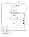
図1は、図4との対比により本発明の実施の形態に係る液晶表示装置を示すブロック図である。この液晶表示装置21において、図4について上述した液晶表示装置1と同一の構成は、対応する符号を付して示し、重複した説明は省略する。
【0020】
この液晶表示装置21は、マトリックス状に画素を配置してなる表示部11と、この表示部11の画素をゲート線LRにより選択して信号線LCにより駆動することにより表示部11に所望の画像を表示する駆動回路12、13とが一体にガラス基板上に形成されるようになされている。また所定のタイミングで信号線LCをプリチャージするプリチャージ回路としてCS駆動回路9がこのガラス基板10上に設けられるようになされている。
【0021】
この液晶表示装置21においては、このプリチャージの処理に係る信号線LC側の配線パターンLCCが、この基板10上でCS駆動回路9に接続され、スイッチ回路16を介して信号線LCに接続される。また保持容量4の信号線側とは逆側の配線パターンである共通線COMが、この信号線LC側の配線パターンLCCと絶縁されて、端子T2に接続され、またこの端子T2に隣接する端子T1に信号線LC側の配線パターンLCCが接続されるようになされている。これによりこの液晶表示装置21では、保持容量4の、信号線LC側とは逆側の電極に接続された電極側の配線パターンCOMが、信号線LCをプリチャージ回路9に接続する信号線側の配線パターンLCCとは絶縁されて、基板10の外部によりプリチャージ回路9に接続されるようになされている。
【0022】
これにより液晶表示装置21では、従来構成に係る液晶表示装置1(図4)とは異なる経路により信号線LCを保持容量4の電位にプリチャージした後、水平駆動回路12、垂直駆動回路13による駆動により各画素を駆動して所望の画像を表示するようになされている。
【0023】
これに対して図2は、検査時におけるこの液晶表示装置21と試験装置22との接続を示すブロック図である。この実施の形態では、ガラス基板10上に各種駆動回路12、13、表示部11等を作成した後、この試験装置22により各種動作試験を実行する。ここでこの動作試験においては、コンピュータ23により試験装置22の動作を制御して、試験装置22から動作基準用のクロック、テストに係る各種表示用のデータを液晶表示装置21に出力して液晶表示装置21の動作を確認することにより実行される。この実施の形態においては、このようにして実行される試験項目の1つに、欠陥画素に係るスクリーニングの試験が設けられる。
【0024】
このスクリーニングの試験において、試験装置22は、スイッチ回路15、16をそれぞれオフ状態、オン状態に設定して、端子T1及びT2を所定電位に設定する。なおこの実施の形態では、例えばこの端子T1及びT2を試験装置22のグランドラインに接続することにより、この所定電位がアース電位に設定される。
【0025】
続いて試験装置22は、端子T2をアース電位より切り離し、図3について上述したパルス状の高電圧を印加する。これによりこの実施の形態では、各画素において、トランジスタ3と保持容量4との間に動作電圧以上の電圧を印加し、市場において欠陥画素に至る画素については、続く欠陥画素の検出処理において、検出可能とするようになされている。
【0026】
しかしてこの実施の形態においては、このように画素の容量4に係る配線パターンLCC、COMのうち、共通線COM側を独立に外部にてプリチャージ回路9に接続することにより、スイッチ回路16には高電圧を印加しないようにしてスクリーニングの試験を実行し得、これにより耐圧の低いトランジスタを用いて構成する場合であっても、信頼性の劣化を有効に回避して確実に欠陥画素に係るスクリーニングを実行することができる。
【0027】
以上の構成によれば、このように画素の容量に係る配線パターンのうち、共通線側を独立に外部にてプリチャージ回路に接続することにより、耐圧の低いトランジスタを用いて構成する場合であっても、信頼性の劣化を有効に回避して確実に欠陥画素に係るスクリーニングを実行することができる。
【0028】
なお上述の実施の形態においては、共通線COMだけを外部接続とする場合について述べたが、本発明はこれに限らず、併せて信号線側の配線パターンLCCについても外部でSC駆動回路に接続するようにしてもよい。
【0029】
また上述の実施の形態においては、ガラス基板上に表示部等を作成してなるTFT液晶に本発明を適用する場合について述べたが、本発明はこれに限らず、CGS(Continuous Grain Silicon)液晶等、各種の液晶表示装置、さらにはEL(Electro Luminescence)表示装置等、種々のフラットディスプレイ装置に広く適用することができる。
【0030】
【発明の効果】
上述のように本発明によれば、画素の容量に係る配線パターンのうち、共通線側を独立に外部にてプリチャージ回路に接続することにより、耐圧の低いトランジスタを用いて構成する場合であっても、信頼性の劣化を有効に回避して確実に欠陥画素に係るスクリーニングを実行することができる。
【図面の簡単な説明】
【図1】本発明の実施の形態に係る液晶表示装置を示すブロック図である。
【図2】図1の液晶表示装置の試験の説明に供するブロック図である。
【図3】欠陥画素のスクリーニングの説明に供する接続図である。
【図4】従来の液晶表示装置を示すブロック図である。
【符号の説明】
1、21……液晶表示装置、2……液晶セル、3……TFT、4……保持容量、9……CS駆動回路、10……ガラス基板、11……表示部、15、16……スイッチ回路[0001]
BACKGROUND OF THE INVENTION
The present invention relates to a flat display device and a test method for the flat display device, and can be applied to, for example, a liquid crystal display device in which a drive circuit is integrally formed on an insulating substrate. In the present invention, the wiring pattern relating to the capacitance of the pixel is connected to the precharge circuit externally independently on the common line side, so that reliability can be ensured even in the case of using a transistor with a low breakdown voltage. It is possible to effectively perform the screening related to the defective pixel by effectively avoiding the deterioration.
[0002]
[Prior art]
In recent years, in a liquid crystal display device which is a flat display device applied to a portable terminal device such as a PDA or a mobile phone, a driving circuit for the liquid crystal display panel is integrated on a glass substrate which is an insulating substrate constituting the liquid crystal display panel. What is configured is to be provided.
[0003]
In such a liquid crystal display device, each pixel is formed by a liquid crystal cell, a polysilicon TFT (Thin Film Transistor) which is a switching element of the liquid crystal cell, and a storage capacitor, and the pixels are arranged in a matrix form for display. The display unit is formed, and the display unit is driven by various drive circuits arranged around the display unit to display various images.
[0004]
In the liquid crystal display device, when even one of the pixels arranged in a matrix is defective, the defective pixel is observed as a bright luminescent spot, and the quality of the display image is significantly impaired. For this reason, various methods for detecting this type of defective pixel have been proposed in Japanese Patent Application Laid-Open No. 2002-221547.
[0005]
[Patent Document 1]
Japanese Patent Laid-Open No. 2002-221547 [0006]
[Problems to be solved by the invention]
By the way, in some liquid crystal display devices, defective pixels are generated by use in the market even if defective pixels are not detected by inspection at the time of shipment. As a result, the applicant of the present application can detect defective pixels generated in this kind of market at the time of shipping inspection by screening by an accelerated test.
[0007]
That is, as shown in FIG. 3, in the liquid crystal display device, each pixel is formed by the
[0008]
Therefore, as shown in FIG. 4, in this type of liquid
[0009]
That is, in the liquid
[0010]
The liquid
[0011]
In the screening test, in a state where the connection between the terminals T1 and T2 is cut off, the
[0012]
However, in such a test method, a pulsed high voltage is applied not only to the storage capacitor 4 but also to the
[0013]
The present invention has been made in consideration of the above points, and even in the case of using a transistor with a low withstand voltage, it is possible to effectively avoid the deterioration of reliability and reliably carry out screening relating to defective pixels. It is intended to propose a flat display device and a test method for the flat display device.
[0014]
[Means for Solving the Problems]
In order to solve such a problem, in the first aspect of the invention, a display unit in which pixels are arranged in a matrix and a pixel in the display unit is selected by a gate line and driven by a signal line to thereby obtain a desired display unit. The present invention is applied to a flat display device in which a drive circuit for displaying an image is integrally formed on a substrate. In the first aspect of the present invention, the pixel line has a precharge circuit for precharging the signal line at a predetermined timing, the pixel has a capacity charged by the potential of the signal line by selection by the gate line, and at least the capacity of The wiring pattern on the electrode side connected to the electrode on the opposite side to the signal line side is insulated from the wiring pattern on the signal line side that connects the signal line to the precharge circuit, and connected to the precharge circuit outside the substrate To be.
[0015]
According to a third aspect of the present invention, there is provided a display unit in which pixels are arranged in a matrix, and driving for displaying a desired image on the display unit by selecting a pixel of the display unit by a gate line and driving it by a signal line. The present invention is applied to a test method for a flat display device in which a circuit is integrally formed on a substrate. According to a third aspect of the present invention, the flat display device has a precharge circuit for precharging the signal line at a predetermined timing, and the pixel has a capacity charged by the potential of the signal line by selection by the gate line. The wiring pattern on the electrode side connected to the electrode opposite to the signal line side of at least the capacitance is insulated from the wiring pattern on the signal line side connecting the signal line to the precharge circuit, A test method for a flat display device connected to a precharge circuit is a pulse-like method between a part where an electrode-side wiring pattern is drawn out of a substrate and a part where asignal line-side wiring pattern is connected to a precharge circuit. It is possible to detect a location related to a pixel defect by applying a voltage.
[0016]
According to the configuration of the first aspect, a display unit in which pixels are arranged in a matrix form, and a drive circuit that displays a desired image on the display unit by selecting pixels of the display unit by gate lines and driving them by signal lines Is applied to a flat display device formed integrally on a substrate, and has a precharge circuit that precharges a signal line at a predetermined timing, and the pixel is charged by the potential of the signal line by selection by the gate line. The wiring pattern on the electrode side connected to the electrode opposite to the signal line side of the capacitor is insulated from the wiring pattern on the signal line side connecting the signal line to the precharge circuit. If the precharge circuit is connected to the outside of the substrate, the external connection portion is cut off and the signal line side is held at a predetermined potential, and the wiring pattern on the electrode side is connected. By applying the scan-like voltage, high voltage so as not applied to the signal line side can perform a test screening. As a result, the application of high voltage can be avoided for active by TFT etc. provided on the signal line side, and even if it is configured using active elements with low withstand voltage, deterioration of reliability is effectively avoided. Thus, screening related to the defective pixel can be executed reliably.
[0017]
Thereby, according to the structure of
[0018]
DETAILED DESCRIPTION OF THE INVENTION
Hereinafter, embodiments of the present invention will be described in detail with reference to the drawings as appropriate.
[0019]
FIG. 1 is a block diagram showing a liquid crystal display device according to an embodiment of the present invention in comparison with FIG. In this liquid
[0020]
The liquid
[0021]
In the liquid
[0022]
As a result, in the liquid
[0023]
On the other hand, FIG. 2 is a block diagram showing the connection between the liquid
[0024]
In this screening test, the
[0025]
Subsequently, the
[0026]
In this embodiment, therefore, the common line COM side of the wiring patterns LCC and COM related to the capacitor 4 of the pixel is connected to the precharge circuit 9 outside independently in this way. Can perform a screening test without applying a high voltage, thereby effectively avoiding deterioration of reliability even when a transistor with a low withstand voltage is used. Screening can be performed.
[0027]
According to the above configuration, in the wiring pattern related to the capacitance of the pixel as described above, the common line side is independently connected to the precharge circuit externally, so that a transistor with a low breakdown voltage is used. However, it is possible to effectively avoid the deterioration of the reliability and execute the screening related to the defective pixel with certainty.
[0028]
In the above-described embodiment, the case where only the common line COM is externally connected has been described. However, the present invention is not limited to this, and the wiring pattern LCC on the signal line side is also externally connected to the SC drive circuit. You may make it do.
[0029]
In the above-described embodiment, the case where the present invention is applied to a TFT liquid crystal in which a display portion or the like is formed on a glass substrate has been described. However, the present invention is not limited to this, and a CGS (Continuous Grain Silicon) liquid crystal is used. The present invention can be widely applied to various flat display devices such as various liquid crystal display devices and EL (Electro Luminescence) display devices.
[0030]
【The invention's effect】
As described above, according to the present invention, among the wiring patterns related to the capacitance of the pixel, the common line side is independently connected to the precharge circuit externally so that a transistor with a low breakdown voltage is used. However, it is possible to effectively avoid the deterioration of the reliability and execute the screening related to the defective pixel with certainty.
[Brief description of the drawings]
FIG. 1 is a block diagram showing a liquid crystal display device according to an embodiment of the present invention.
FIG. 2 is a block diagram for explaining a test of the liquid crystal display device of FIG. 1;
FIG. 3 is a connection diagram for explaining defective pixel screening;
FIG. 4 is a block diagram showing a conventional liquid crystal display device.
[Explanation of symbols]
DESCRIPTION OF
Claims (3)
Translated fromJapanese所定のタイミングで前記信号線をプリチャージするプリチャージ回路を有し、
前記画素が、
前記ゲート線による選択により前記信号線の電位により充電される容量を有し、
少なくとも前記容量の、前記信号線側とは逆側の電極に接続された電極側の配線パターンが、前記信号線を前記プリチャージ回路に接続する信号線側の配線パターンとは絶縁されて、前記基板の外部により前記プリチャージ回路に接続される
ことを特徴とするフラットディスプレイ装置。A display unit in which pixels are arranged in a matrix and a drive circuit that displays a desired image on the display unit by selecting the pixels of the display unit by gate lines and driving them by signal lines are integrally formed on a substrate. In the flat display device formed in
A precharge circuit for precharging the signal line at a predetermined timing;
The pixel is
A capacitor charged by the potential of the signal line by selection by the gate line;
The wiring pattern on the electrode side connected to the electrode opposite to the signal line side of at least the capacitor is insulated from the wiring pattern on the signal line side connecting the signal line to the precharge circuit, and A flat display device connected to the precharge circuit from outside the substrate.
前記アクティブ素子が、低温ポリシリコン又はCGSによる素子である
ことを特徴とする請求項1に記載のフラットディスプレイ装置。The wiring pattern on the signal line side is connected to the signal line via a switch circuit by an active element,
The flat display device according to claim 1, wherein the active element is an element made of low-temperature polysilicon or CGS.
前記フラットディスプレイ装置は、
所定のタイミングで前記信号線をプリチャージするプリチャージ回路を有し、
前記画素が、
前記ゲート線による選択により前記信号線の電位により充電される容量を有し、
少なくとも前記容量の、前記信号線側とは逆側の電極に接続された電極側の配線パターンが、前記信号線を前記プリチャージ回路に接続する信号線側の配線パターンとは絶縁されて、前記基板の外部により前記プリチャージ回路に接続され、
前記フラットディスプレイ装置の試験方法は、
前記電極側の配線パターンを前記基板の外部に引き出す箇所と、前記信号線側の配線パターンを前記プリチャージ回路に接続する箇所との間でパルス状の電圧を印加して前記画素の欠陥に係る箇所を検出可能とする
ことを特徴とするフラットディスプレイ装置の試験方法。A display unit in which pixels are arranged in a matrix and a drive circuit that displays a desired image on the display unit by selecting the pixels of the display unit by gate lines and driving them by signal lines are integrally formed on a substrate. In the test method of the flat display device formed in
The flat display device is:
A precharge circuit for precharging the signal line at a predetermined timing;
The pixel is
A capacitor charged by the potential of the signal line by selection by the gate line;
The wiring pattern on the electrode side connected to the electrode opposite to the signal line side of at least the capacitor is insulated from the wiring pattern on the signal line side connecting the signal line to the precharge circuit, and Connected to the precharge circuit by the outside of the substrate,
The test method of the flat display device is:
A pulse-like voltage is applied between a location where the wiring pattern on the electrode side is drawn out of the substrate and a location wherethe wiring patternon the signal line side is connected to the precharge circuit. A test method for a flat display device, characterized in that the location can be detected.
Priority Applications (6)
| Application Number | Priority Date | Filing Date | Title |
|---|---|---|---|
| JP2003186430AJP3968713B2 (en) | 2003-06-30 | 2003-06-30 | Flat display device and testing method of flat display device |
| SG200403676-0ASG148018A1 (en) | 2003-06-30 | 2004-06-23 | Flat display apparatus and flat display apparatus testing method |
| KR1020040047597AKR101024621B1 (en) | 2003-06-30 | 2004-06-24 | Flat display device and test method of flat display device |
| TW093118890ATWI254907B (en) | 2003-06-30 | 2004-06-28 | Flat display apparatus and flat display apparatus testing method |
| US10/876,450US7639034B2 (en) | 2003-06-30 | 2004-06-28 | Flat display apparatus and flat display apparatus testing method |
| CNB2004100625451ACN100354918C (en) | 2003-06-30 | 2004-06-30 | Flat display apparatus and flat display apparatus testing method |
Applications Claiming Priority (1)
| Application Number | Priority Date | Filing Date | Title |
|---|---|---|---|
| JP2003186430AJP3968713B2 (en) | 2003-06-30 | 2003-06-30 | Flat display device and testing method of flat display device |
Publications (2)
| Publication Number | Publication Date |
|---|---|
| JP2005017989A JP2005017989A (en) | 2005-01-20 |
| JP3968713B2true JP3968713B2 (en) | 2007-08-29 |
Family
ID=34100166
Family Applications (1)
| Application Number | Title | Priority Date | Filing Date |
|---|---|---|---|
| JP2003186430AExpired - LifetimeJP3968713B2 (en) | 2003-06-30 | 2003-06-30 | Flat display device and testing method of flat display device |
Country Status (6)
| Country | Link |
|---|---|
| US (1) | US7639034B2 (en) |
| JP (1) | JP3968713B2 (en) |
| KR (1) | KR101024621B1 (en) |
| CN (1) | CN100354918C (en) |
| SG (1) | SG148018A1 (en) |
| TW (1) | TWI254907B (en) |
Families Citing this family (9)
| Publication number | Priority date | Publication date | Assignee | Title |
|---|---|---|---|---|
| JP4615276B2 (en)* | 2004-09-21 | 2011-01-19 | シャープ株式会社 | Content data distribution apparatus and content data distribution system |
| US8836621B2 (en)* | 2004-12-15 | 2014-09-16 | Nlt Technologies, Ltd. | Liquid crystal display apparatus, driving method for same, and driving circuit for same |
| JP2008164289A (en)* | 2005-05-18 | 2008-07-17 | Koninkl Philips Electronics Nv | Liquid crystal display testing circuit, liquid crystal display built in with the same, and liquid crystal display testing method |
| TWI357981B (en)* | 2007-01-30 | 2012-02-11 | Au Optronics Corp | Testing system and method of liquid crystal displa |
| CN100485472C (en)* | 2007-08-31 | 2009-05-06 | 友达光电股份有限公司 | Liquid crystal display with pre-charging circuit |
| CN105788501B (en)* | 2016-05-20 | 2019-12-10 | 京东方科技集团股份有限公司 | Organic electroluminescent display panel, aging test device, aging test method and display device |
| CN110310608B (en)* | 2018-03-27 | 2021-01-05 | 京东方科技集团股份有限公司 | Control circuit, test equipment and test method of liquid crystal display panel |
| WO2020003445A1 (en)* | 2018-06-28 | 2020-01-02 | 堺ディスプレイプロダクト株式会社 | Display panel, method for inspecting display panel, and method for manufacturing display panel |
| CN109889278A (en)* | 2019-02-20 | 2019-06-14 | 维沃移动通信有限公司 | Mobile terminal and method for improving call quality |
Family Cites Families (26)
| Publication number | Priority date | Publication date | Assignee | Title |
|---|---|---|---|---|
| JPH0272392A (en)* | 1988-09-07 | 1990-03-12 | Hitachi Ltd | Inspecting and correcting method for active matrix type display device |
| JPH06183561A (en) | 1992-12-18 | 1994-07-05 | Canon Inc | Moving stage device |
| JP3086764B2 (en) | 1993-02-22 | 2000-09-11 | キヤノン株式会社 | Hydrostatic bearing device |
| JP3164960B2 (en) | 1994-02-18 | 2001-05-14 | キヤノン株式会社 | Stage equipment |
| JPH08229759A (en) | 1995-02-24 | 1996-09-10 | Canon Inc | Positioning device and device manufacturing apparatus and method |
| JP3634483B2 (en) | 1996-02-13 | 2005-03-30 | キヤノン株式会社 | Stage apparatus, and exposure apparatus and device production method using the same |
| JP3635600B2 (en) | 1996-08-29 | 2005-04-06 | キヤノン株式会社 | Feeder |
| JP3907252B2 (en) | 1996-12-05 | 2007-04-18 | キヤノン株式会社 | Exposure apparatus, device manufacturing method, stage apparatus, and origin finding method |
| US6028376A (en) | 1997-04-22 | 2000-02-22 | Canon Kabushiki Kaisha | Positioning apparatus and exposure apparatus using the same |
| JP3648976B2 (en)* | 1998-03-24 | 2005-05-18 | セイコーエプソン株式会社 | Active matrix substrate, liquid crystal device, electronic apparatus, and inspection method of active matrix substrate |
| JP4081852B2 (en)* | 1998-04-30 | 2008-04-30 | ソニー株式会社 | Matrix driving method for organic EL element and matrix driving apparatus for organic EL element |
| JP3413122B2 (en) | 1998-05-21 | 2003-06-03 | キヤノン株式会社 | Positioning apparatus, exposure apparatus using the same, and device manufacturing method |
| KR100324914B1 (en)* | 1998-09-25 | 2002-02-28 | 니시무로 타이죠 | Test method of substrate |
| TW521241B (en)* | 1999-03-16 | 2003-02-21 | Sony Corp | Liquid crystal display apparatus, its driving method, and liquid crystal display system |
| JP4894081B2 (en)* | 2000-06-14 | 2012-03-07 | ソニー株式会社 | Display device and driving method thereof |
| JP2002075855A (en) | 2000-06-14 | 2002-03-15 | Canon Inc | Self-weight compensator, stage apparatus using the same, exposure apparatus and device manufacturing method using the same |
| JP4473427B2 (en) | 2000-08-03 | 2010-06-02 | エーユー オプトロニクス コーポレイション | Array substrate inspection method and inspection apparatus |
| JP2002280283A (en) | 2001-03-16 | 2002-09-27 | Canon Inc | Substrate processing equipment |
| JP2002349569A (en) | 2001-05-25 | 2002-12-04 | Canon Inc | Hydrostatic bearing device and stage device using the same |
| TW511047B (en)* | 2001-06-12 | 2002-11-21 | Prime View Int Co Ltd | Scan driving circuit and method for an active matrix liquid crystal display |
| KR100819138B1 (en)* | 2001-08-25 | 2008-04-21 | 엘지.필립스 엘시디 주식회사 | Driving device of electroluminescence panel and driving method thereof |
| US6638787B1 (en)* | 2001-12-04 | 2003-10-28 | Pulnix America, Inc. | High-frame-rate CCD imaging devices made in low-production runs from otherwise ordinary and inexpensive CCD devices |
| JP3714243B2 (en)* | 2001-12-11 | 2005-11-09 | セイコーエプソン株式会社 | Semiconductor device, electro-optical device, and electronic apparatus |
| KR100421053B1 (en)* | 2002-02-22 | 2004-03-04 | 삼성전자주식회사 | Precharge Method and Precharge voltage generation circuit of signal line |
| TW577135B (en)* | 2002-10-21 | 2004-02-21 | Au Optronics Corp | Die size control for polysilicon film and the inspection method thereof |
| US6999051B2 (en)* | 2003-06-11 | 2006-02-14 | Toppoly Optoelectronics Corp. | Light-on aging test system for flat panel display |
- 2003
- 2003-06-30JPJP2003186430Apatent/JP3968713B2/ennot_activeExpired - Lifetime
- 2004
- 2004-06-23SGSG200403676-0Apatent/SG148018A1/enunknown
- 2004-06-24KRKR1020040047597Apatent/KR101024621B1/ennot_activeExpired - Lifetime
- 2004-06-28USUS10/876,450patent/US7639034B2/enactiveActive
- 2004-06-28TWTW093118890Apatent/TWI254907B/ennot_activeIP Right Cessation
- 2004-06-30CNCNB2004100625451Apatent/CN100354918C/ennot_activeExpired - Lifetime
Also Published As
| Publication number | Publication date |
|---|---|
| US20050024306A1 (en) | 2005-02-03 |
| TWI254907B (en) | 2006-05-11 |
| SG148018A1 (en) | 2008-12-31 |
| CN100354918C (en) | 2007-12-12 |
| US7639034B2 (en) | 2009-12-29 |
| JP2005017989A (en) | 2005-01-20 |
| CN1577469A (en) | 2005-02-09 |
| KR101024621B1 (en) | 2011-03-25 |
| KR20050005775A (en) | 2005-01-14 |
| TW200514011A (en) | 2005-04-16 |
Similar Documents
| Publication | Publication Date | Title |
|---|---|---|
| US7456647B2 (en) | Liquid crystal display panel and testing and manufacturing methods thereof | |
| JP4006304B2 (en) | Image display device | |
| US6909304B2 (en) | Display device and scanning circuit testing method | |
| US20070080913A1 (en) | Display device and testing method for display device | |
| US20020070750A1 (en) | Test method of electro-optical device, test circuit of electro-optical device, electro-optical device, and electronic equipment | |
| US7705819B2 (en) | Display device | |
| US20060119755A1 (en) | Liquid crystal display device | |
| JP3968713B2 (en) | Flat display device and testing method of flat display device | |
| JPH01130131A (en) | Driver-containing active matrix panel | |
| JP3424302B2 (en) | Liquid crystal display | |
| JP4637868B2 (en) | Image display device | |
| JP2010243644A (en) | Display device and inspection device | |
| JP2003157053A (en) | Liquid crystal display device, its inspection method and its inspection device | |
| JP2002258231A (en) | Liquid crystal display substrate, information terminal device, liquid crystal display substrate inspection device, liquid crystal display substrate inspection method, and program | |
| JP3177702B2 (en) | Inspection method of liquid crystal display | |
| JP4661293B2 (en) | Display device defect detection method and display device defect detection device | |
| JP2010243643A (en) | Display device and inspection device | |
| JPH1082814A (en) | Image display device and inspection method of image display device | |
| JP2003114658A (en) | Display device and inspection method thereof | |
| JP3191898B2 (en) | Inspection method for thin film transistor array | |
| JP2001033813A (en) | Inspection method of liquid crystal display | |
| JPH0980478A (en) | Defect detection method for matrix type display device | |
| JP2001352072A (en) | Thin film transistor array | |
| KR20050031278A (en) | Test device for examining a panel of liquid crystal display device | |
| KR20040060024A (en) | Frame and the driving method for TFT bias-aging |
Legal Events
| Date | Code | Title | Description |
|---|---|---|---|
| A621 | Written request for application examination | Free format text:JAPANESE INTERMEDIATE CODE: A621 Effective date:20041224 | |
| A977 | Report on retrieval | Free format text:JAPANESE INTERMEDIATE CODE: A971007 Effective date:20070115 | |
| A131 | Notification of reasons for refusal | Free format text:JAPANESE INTERMEDIATE CODE: A131 Effective date:20070117 | |
| A521 | Request for written amendment filed | Free format text:JAPANESE INTERMEDIATE CODE: A523 Effective date:20070316 | |
| TRDD | Decision of grant or rejection written | ||
| A01 | Written decision to grant a patent or to grant a registration (utility model) | Free format text:JAPANESE INTERMEDIATE CODE: A01 Effective date:20070511 | |
| A61 | First payment of annual fees (during grant procedure) | Free format text:JAPANESE INTERMEDIATE CODE: A61 Effective date:20070524 | |
| R151 | Written notification of patent or utility model registration | Ref document number:3968713 Country of ref document:JP Free format text:JAPANESE INTERMEDIATE CODE: R151 | |
| FPAY | Renewal fee payment (event date is renewal date of database) | Free format text:PAYMENT UNTIL: 20100615 Year of fee payment:3 | |
| FPAY | Renewal fee payment (event date is renewal date of database) | Free format text:PAYMENT UNTIL: 20100615 Year of fee payment:3 | |
| FPAY | Renewal fee payment (event date is renewal date of database) | Free format text:PAYMENT UNTIL: 20110615 Year of fee payment:4 | |
| R250 | Receipt of annual fees | Free format text:JAPANESE INTERMEDIATE CODE: R250 | |
| FPAY | Renewal fee payment (event date is renewal date of database) | Free format text:PAYMENT UNTIL: 20120615 Year of fee payment:5 | |
| R250 | Receipt of annual fees | Free format text:JAPANESE INTERMEDIATE CODE: R250 | |
| FPAY | Renewal fee payment (event date is renewal date of database) | Free format text:PAYMENT UNTIL: 20130615 Year of fee payment:6 | |
| R250 | Receipt of annual fees | Free format text:JAPANESE INTERMEDIATE CODE: R250 | |
| FPAY | Renewal fee payment (event date is renewal date of database) | Free format text:PAYMENT UNTIL: 20130615 Year of fee payment:6 | |
| S111 | Request for change of ownership or part of ownership | Free format text:JAPANESE INTERMEDIATE CODE: R313113 | |
| FPAY | Renewal fee payment (event date is renewal date of database) | Free format text:PAYMENT UNTIL: 20130615 Year of fee payment:6 | |
| R350 | Written notification of registration of transfer | Free format text:JAPANESE INTERMEDIATE CODE: R350 | |
| R250 | Receipt of annual fees | Free format text:JAPANESE INTERMEDIATE CODE: R250 | |
| R250 | Receipt of annual fees | Free format text:JAPANESE INTERMEDIATE CODE: R250 | |
| R250 | Receipt of annual fees | Free format text:JAPANESE INTERMEDIATE CODE: R250 | |
| R250 | Receipt of annual fees | Free format text:JAPANESE INTERMEDIATE CODE: R250 | |
| R250 | Receipt of annual fees | Free format text:JAPANESE INTERMEDIATE CODE: R250 | |
| R250 | Receipt of annual fees | Free format text:JAPANESE INTERMEDIATE CODE: R250 | |
| R250 | Receipt of annual fees | Free format text:JAPANESE INTERMEDIATE CODE: R250 | |
| R250 | Receipt of annual fees | Free format text:JAPANESE INTERMEDIATE CODE: R250 | |
| S111 | Request for change of ownership or part of ownership | Free format text:JAPANESE INTERMEDIATE CODE: R313111 | |
| R250 | Receipt of annual fees | Free format text:JAPANESE INTERMEDIATE CODE: R250 | |
| R350 | Written notification of registration of transfer | Free format text:JAPANESE INTERMEDIATE CODE: R350 | |
| R250 | Receipt of annual fees | Free format text:JAPANESE INTERMEDIATE CODE: R250 | |
| R250 | Receipt of annual fees | Free format text:JAPANESE INTERMEDIATE CODE: R250 | |
| EXPY | Cancellation because of completion of term |