JP3968187B2 - Semiconductor device and manufacturing method thereof - Google Patents
Semiconductor device and manufacturing method thereofDownload PDFInfo
- Publication number
- JP3968187B2 JP3968187B2JP08823599AJP8823599AJP3968187B2JP 3968187 B2JP3968187 B2JP 3968187B2JP 08823599 AJP08823599 AJP 08823599AJP 8823599 AJP8823599 AJP 8823599AJP 3968187 B2JP3968187 B2JP 3968187B2
- Authority
- JP
- Japan
- Prior art keywords
- semiconductor device
- trimming
- adjustment circuit
- laser
- semiconductor chip
- Prior art date
- Legal status (The legal status is an assumption and is not a legal conclusion. Google has not performed a legal analysis and makes no representation as to the accuracy of the status listed.)
- Expired - Fee Related
Links
Images


Classifications
- H—ELECTRICITY
- H01—ELECTRIC ELEMENTS
- H01L—SEMICONDUCTOR DEVICES NOT COVERED BY CLASS H10
- H01L2224/00—Indexing scheme for arrangements for connecting or disconnecting semiconductor or solid-state bodies and methods related thereto as covered by H01L24/00
- H01L2224/01—Means for bonding being attached to, or being formed on, the surface to be connected, e.g. chip-to-package, die-attach, "first-level" interconnects; Manufacturing methods related thereto
- H01L2224/42—Wire connectors; Manufacturing methods related thereto
- H01L2224/47—Structure, shape, material or disposition of the wire connectors after the connecting process
- H01L2224/48—Structure, shape, material or disposition of the wire connectors after the connecting process of an individual wire connector
- H01L2224/4805—Shape
- H01L2224/4809—Loop shape
- H01L2224/48091—Arched
- H—ELECTRICITY
- H01—ELECTRIC ELEMENTS
- H01L—SEMICONDUCTOR DEVICES NOT COVERED BY CLASS H10
- H01L2224/00—Indexing scheme for arrangements for connecting or disconnecting semiconductor or solid-state bodies and methods related thereto as covered by H01L24/00
- H01L2224/01—Means for bonding being attached to, or being formed on, the surface to be connected, e.g. chip-to-package, die-attach, "first-level" interconnects; Manufacturing methods related thereto
- H01L2224/42—Wire connectors; Manufacturing methods related thereto
- H01L2224/47—Structure, shape, material or disposition of the wire connectors after the connecting process
- H01L2224/48—Structure, shape, material or disposition of the wire connectors after the connecting process of an individual wire connector
- H01L2224/481—Disposition
- H01L2224/48151—Connecting between a semiconductor or solid-state body and an item not being a semiconductor or solid-state body, e.g. chip-to-substrate, chip-to-passive
- H01L2224/48221—Connecting between a semiconductor or solid-state body and an item not being a semiconductor or solid-state body, e.g. chip-to-substrate, chip-to-passive the body and the item being stacked
- H01L2224/48245—Connecting between a semiconductor or solid-state body and an item not being a semiconductor or solid-state body, e.g. chip-to-substrate, chip-to-passive the body and the item being stacked the item being metallic
- H01L2224/48247—Connecting between a semiconductor or solid-state body and an item not being a semiconductor or solid-state body, e.g. chip-to-substrate, chip-to-passive the body and the item being stacked the item being metallic connecting the wire to a bond pad of the item
- H—ELECTRICITY
- H01—ELECTRIC ELEMENTS
- H01L—SEMICONDUCTOR DEVICES NOT COVERED BY CLASS H10
- H01L2924/00—Indexing scheme for arrangements or methods for connecting or disconnecting semiconductor or solid-state bodies as covered by H01L24/00
- H01L2924/15—Details of package parts other than the semiconductor or other solid state devices to be connected
- H01L2924/181—Encapsulation
Landscapes
- Laser Beam Processing (AREA)
- Structures Or Materials For Encapsulating Or Coating Semiconductor Devices Or Solid State Devices (AREA)
- Semiconductor Integrated Circuits (AREA)
- Design And Manufacture Of Integrated Circuits (AREA)
Description
Translated fromJapanese【0001】
【発明の属する技術分野】
本発明は、半導体装置の製造方法及び半導体装置に関し、特に、レーザートリミングを用いて素子調整値の変更が可能な調整回路が半導体チップ上に形成されている半導体装置及びその製造方法に関する。
【0002】
【従来の技術】
従来この種の半導体装置としては、例えば、実開平6−13148号公報に示すようなものがある(以下、第1従来技術と呼ぶ、図3参照)。
【0003】
すなわち、透明のプラスチックでモールドされたICであって、ウェハーチップの見える部分1Aだけ紫外光が透過するようにし、それ以外の部分が外部光を遮断するように塗装、印刷、蒸着等によって覆われた構造を有する半導体装置である。ここでは、EP−ROM等のICに紫外線を透明なプラスチックパッケージの外部から照射してEP−ROM(紫外線消去型ROM)の記憶内容を消去することが開示されている。
【0004】
また、従来この種の半導体装置の製造方法としては、例えば、特開平5−94905号公報に示すようなものがある(以下、第2従来技術と呼ぶ、図4参照)。
【0005】
すなわち、半導体装置2Bを光学的に不透明な樹脂5Bで被覆した後に、抵抗体3Bにレーザ光を照射して半導体装置2Bと共に基板1B上に形成された抵抗体3Bの一部をレーザ光でカットする抵抗体トリミング方法である。これにより、微調整済みの調整値がずれないように抵抗体3Bをトリミングできることが示されている。更に、レーザ光は光学的に不透明な樹脂5Bにより遮断され、樹脂5Bに覆われた半導体装置2Bはレーザ光の影響を受けなくなるといった効果が開示されている。
【0006】
一方、レーザートリミングを要するIC(半導体装置)では、レーザートリミングヒューズや配線をレーザーでトリミングすることで電圧、電流、周波数等を微調整している。
【0007】
ここで、トリミングとは、一般的にヒューズや配線を切削する、即ち切断又はその一部分を削り取ることを意味するが、配線等を接続や溶接することも可能である。
【0008】
このような半導体装置において、レーザーレーザートリミングはウェハ状態で行われ、その後、アセンブリ工程を経てパッケージに組み立てられる。
【0009】
具体的には、レーザートリミングを用いて素子調整値の変更が可能な調整回路が半導体チップ上に形成されている半導体装置をユーザに製品出荷やサンプル出荷する場合、定電圧源の電圧値、定電流源の電流値、動作周波数等の特性値(素子調整値)のユーザ先からの指定に応じて調整回路の素子調整値を変更する作業(以降、ユーザカスタマイズ作業工程と呼ぶ)を行うことが必要となる(以下、第3従来技術と呼ぶ)。
【0010】
このようなユーザカスタマイズ作業工程を行う場合、ウェハー上に形成されている半導体チップに対してユーザの要求に応じたレーザートリミングを実行した後、アセンブリを行い、最後にファイナルテストを実行し、合格した半導体装置をユーザに製品出荷やサンプル出荷していた。
【0011】
ここで、アセンブリとは、半導体チップをウェハーから切り出し、切り出した半導体チップをタブ上にマウントする作業を行い、続いて、マウントされた半導体チップとリードフレームとをワイヤーボンド接続し、続いて、ワイヤーボンド接続の済んだ半導体チップをモールド材等を用いてパッケージ化する工程を意味する。
【0012】
また、ファイナルテストとは、アセンブリ工程を行った後のパッケージ化された半導体チップが、ユーザの要求に応じた素子調整値になっているか否かを試験する工程を意味する。
【0013】
【発明が解決しようとする課題】
しかしながら、このような第1従来技術は、ウェハーチップの見える部分1Aだけ透過する光が紫外光であり、この紫外光を用いたEP−ROMの記憶内容の消去を目的としており、素子調整値の変更が可能な調整回路が半導体チップ上に形成されている半導体装置に呈するレーザートリミングとは適用技術分野が異なる。
【0014】
また、第2従来技術は、樹脂5Bは半導体装置2Bからレーザ光を光学的に遮断するために用いられている遮蔽物であり、このような樹脂5Bを介したレーザートリミングは不可能であるという問題点があった。
【0015】
一方第3従来技術は、ユーザカスタマイズ作業工程を行う場合、レーザートリミングを実行した後、アセンブリ及びファイナルテストを実行し、合格した半導体装置をユーザに製品出荷やサンプル出荷していたため、ユーザから受注してから実際にサンプル品をユーザに納品するまでに1から3カ月程度を要してして納期が長くなってしまい、ユーザからの注文に即応した迅速な製品出荷やサンプル出荷ができず、高い顧客満足を得ることが難しいという技術的課題があった。
【0016】
第3従来技術において、ユーザ先への納期を短くしようとした場合、ユーザの要求を予想した各種の特性値のサンプル在庫を常時ストックしておく必要が性が生じ、半導体装置の在庫量が膨大な量となってしまうという弊害があった。また、レーザートリミング→アセンブリ→ファイナルテストの順番でユーザからの依頼がある度にユーザカスタマイズ作業工程をおこなっていたのでは、アセンブリ工程での時間が長くかかるために、非常に生産性が悪いという技術的課題があった。
また、第3従来技術は、レーザートリミング後にパッケージ化を行っているため、モールド材等と半導体チップとの間で発生する応力によってトリミング当初の設定値が経時変化してしまった場合に再びトリミングを実行することができないというという技術的課題があった。
【0017】
本発明は、このような従来の問題点を解決することを課題としており、特に、レーザートリミングを全くまたは一部だけ実行していない半導体チップに対してアセンブリを行い、少量の半導体装置を予め作成してストックしておき、ユーザからの注文を受けた場合に、ユーザが要求する素子調整値に応じたレーザートリミングを実行するようなユーザカスタマイズ作業工程を実行し、続いて、ファイナルテストを実行し、合格した半導体装置をユーザに製品出荷やサンプル出荷することにより、ユーザから受注した後にサンプル品をユーザに納品するまでの期間を数日程度までに短縮した生産性の向上を実現し、ユーザからの注文に即応した迅速な製品出荷やサンプル出荷を実現して高い顧客満足を得ることを目的としている。
【0018】
更に、ユーザ先への納期の短縮を図ることにより、ユーザの要求を予想した各種の特性値のサンプル在庫を常時ストックしておく必要性を無くし、半導体装置の在庫量の縮小が可能となる。
【0019】
更に、モールド材等と半導体チップとの間で発生する応力によってトリミング当初の設定値が経時変化してしまった場合であっても、再びトリミングを実行することができるようにすることを目的としている。
【0020】
【課題を解決するための手段】
上記課題を解決するため成された請求項1は、レーザートリミングを用いて素子調整値の変更が可能な調整回路が半導体チップ上に形成されている半導体装置において、
透明性樹脂材料で封止された半導体パッケージの梨子地状の表面に、所定波長範囲のレーザービームに対して前記調整回路の一部を切削するのに充分なエネルギーを透過させるために表面を滑らかにする透明性材料による透明化処理が施されている
ことを特徴とする半導体装置である。
【0021】
請求項1に記載の発明によれば、レーザートリミングを全くまたは一部だけ実行していない半導体チップに対してアセンブリを行い、少量の半導体装置を予め作成してストックしておき、ユーザからの注文を受けた場合に、ユーザが要求する素子調整値に応じたレーザートリミングを実行するようなユーザカスタマイズ作業工程を実行し、続いて、ファイナルテストを実行し、合格した半導体装置をユーザに製品出荷やサンプル出荷することができるようになる。
【0022】
これにより、ユーザから受注してから実際にサンプル品をユーザに納品するまでの期間を数日程度までに短縮し、ユーザからの注文に即応した迅速な製品出荷やサンプル出荷を実現し、高い顧客満足を得ることができるようになる。
【0023】
更に、このようにユーザ先への納期の短縮を図ることにより、ユーザの要求を予想した各種の特性値のサンプル在庫を常時ストックしておく必要性を無くし、半導体装置の在庫量の縮小を図ることができるようになる。
更に、モールド材等と半導体チップとの間で発生する応力によってトリミング当初の設定値が経時変化してしまった場合であっても、再びトリミングを実行することができるようになる。
更に、パッケージ表面でレーザービームが散乱されずに半導体チップに照射することができる。
【0024】
また請求項2は、前記透明性材料が、油または水であることを特徴とする請求項1に記載の半導体装置である。
また請求項3は、前記調整回路の一部が前記半導体チップの上面から前記透明性材料および透明性樹脂材料を介して前記調整回路に集光されたレーザービームによって切削されて、前記素子調整値が目標値に設定されていることを特徴とする請求項1または2に記載の半導体装置である。
【0025】
請求項2および3に記載の発明によれば、請求項1に記載の効果と同様の効果を奏する。
【0026】
また請求項4は、レーザートリミングを用いて素子調整値の変更が可能な調整回路が半導体チップ上に形成されている半導体装置の製造方法において、
所定波長範囲のレーザービームに対して前記調整回路の一部を切削するのに充分なエネルギーを透過する透明性樹脂材料を用いて前記半導体チップをパッケージ化する工程と、
前記パッケージ化する工程後に、パッケージの梨子地状の表面のレーザービームを入射する部分を透明性材料により滑らかにする透明化処理工程と、
前記透明化処理工程後に前記レーザービームを前記半導体チップの上面から前記透明性材料および透明性樹脂材料を介して前記調整回路に集光し前記調整回路の一部を切削して前記素子調整値を目標値に設定するトリミング工程と
を有することを特徴とする半導体装置の製造方法である。
【0027】
請求項3に記載の発明によれば、請求項1に記載の効果と同様の効果を奏する。
【0028】
【発明の実施の形態】
(第1実施形態)
初めに、本発明の半導体装置の第1実施形態を説明する。
【0029】
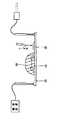
図1は、本発明の半導体装置の第1実施形態を説明するための素子断面図である。
【0030】
図1に示す半導体装置は、レーザートリミングを用いて素子調整値の変更が可能な調整回路12が半導体チップ上に形成され、同時に、前記半導体チップが、所定波長範囲λ1〜λ2のレーザービーム13に対して前記調整回路の一部を切削するのに充分なエネルギーを透過する透明性材料14を用いてパッケージされている点に特徴を有している。
【0031】
トリミングする素子調整値(特性項目)としては、検出電圧値、出力電圧値、発振周波数、出力電流等が挙げられる。
【0032】
半導体装置としては、ボルテージレギュレータIC、ボルテージディテクタIC,DC/DCコンバータIC、定電流IC、定電圧IC等のIC、温度センサー、湿度センサー、ガスセンサー、加速度センサー等が考えられる。以下の説明では、半導体装置をボルテージレギュレータ10とし、半導体チップをボルテージレギュレータチップ11として説明する。
【0033】
このボルテージレギュレータ10に内蔵されているボルテージレギュレータチップ11には、レーザー加工用(レーザートリミング用)のヒューズ、配線又は抵抗素子が、レーザートリミングの対象として形成されている。
【0034】
ここで、ヒューズ又は配線、抵抗は、ボルテージレギュレータチップ11上に形成され、レーザー加工(レーザートリミング)されるものであって、レーザーにより加工されることでボルテージレギュレータチップ11の出力電圧、出力電流、発振周波数、抵抗値、応答速度等の特性を調整できる。
【0035】
ヒューズ又は配線、抵抗の材料としてはアルミニウム(元素記号:Al)、金(元素記号:Au)、銅(元素記号:Cu)、白金(元素記号:Pt)、チタン(元素記号:Ti)、タングステン(元素記号:W)等の金属やポリシリコン、Si拡散層等が用いられる。
【0036】
ヒューズ又は配線、抵抗の上層の保護膜としては、従来より用いられている酸化膜(SiO2)、PSG膜、BPSG膜、窒化膜(SiN)等が適用できる。これらは通常の配線間の絶縁膜やパッシベーション膜をそのまま用いれば良い。望ましくは、これらの中の膜で硬質でない膜質のものを用い、通常と同じかやや厚めの膜厚とするのが良い。又、ポリイミド膜については、レーザビームの透過率を低下させることにつながるので、ヒューズ等の上層の保護膜としてはあまり適さないが、膜厚を薄くすれば適用できる。
【0037】
また、このボルテージレギュレータ10における調整回路としては、具体的には、基準電圧や基準電流の微調整を行うためのラダー抵抗網が考えられる。
【0038】
ここでは、調整回路をラダー抵抗網12とし、レーザートリミングでラダー抵抗網12に対する抵抗値の微調整を行うものとする。
【0039】
使用するレーザは、ヒューズ又は電線抵抗を加工するためのもので、YAGレーザ(基本発振波長=1.06μm)等の固体レーザやCO2レーザ(基本発振波長=10.6μm)等のガスレーザを用いることができる。
【0040】
ここでは、YAGレーザを用いる場合で説明する。YAGレーザは、基本波長がおおよそ1064nmであり、YAGレーザの2次高調波を用いる場合は、レーザートリミング波長はおおよそ532nm(=1064/2)であり、3次高調波を用いる場合は、レーザートリミング波長はおおよそ355nm(=1064/3)である。このため、所定波長範囲λ1〜λ2は300〜1100nm程度となる。
【0041】
次に、第1実施形態の透明性材料14は、おおよそ300〜1100nm程度の所定波長範囲に対して半導体チップ上の調整回路の一部を切削するのに充分なエネルギーを透過する透過率を有している。なお、第1実施形態における透明とは、レーザートリミング波長に対して低い吸収率を有することを意味しており、実用的には、レーザートリミング波長に対して20%以下の吸収率であればよい。ここでは、透明性材料14としてエポキシ樹脂封止剤を用いている。
【0042】
続いて、図1のボルテージレギュレータ10の製造方法の第1実施形態を説明する。
【0043】
図2は、図1のボルテージレギュレータ10の製造方法の第1実施形態を説明するためのプロセス図である。
【0044】
第1実施形態のパッケージの方法としては、トランスファモールド、ポッティング、ディッピング、インジェクションモールド等を用いることができる。尚、これらのパッケージ材料は、パッケージ後に、前述のヒューズ又は配線、抵抗等の上層の保護膜と密着した形態でも良いが、前記保護膜と直接に接触しない状態でパッケージされていて、その空間に不活性ガス等が充填されている形態でも良い。
【0045】
パッケージ形態は、CSP(Chip Size Package)、BGA(Ball Grid Array)パッケージ、QFP(Quad FlatPackage),SOP(Small Outline Package),DIP(Dual Inline Package)等を広く用いることができる。
【0046】
第1実施形態では、先ずアセンブリ工程を行う。すなわち、ウェハーから切り出したボルテージレギュレータチップ11をタブ17上にマウントし、続いて、マウントされたボルテージレギュレータチップ11とリードフレーム16とをボンディングワイヤー15を介してワイヤーボンド接続し、続いて、ワイヤーボンド接続の済んだボルテージレギュレータチップ11をエポキシ樹脂封止剤14を用いてパッケージ化までの工程を行う。
【0047】
次に、レーザートリミングを実施してラダー抵抗網12の抵抗値の変更を行う。
すなわち、ボルテージレギュレータ10は、ボルテージレギュレータチップ11上にラダー抵抗網12が形成されており、レーザトリミングによってその一部を切断して抵抗値を調整する。
【0048】
具体的には、ボルテージレギュレータ10をレーザートリミングしない状態、又は一部レーザートリミングした状態でパッケージ化する。パッケージには、一般に使用されている黒色のエポキシ樹脂封止剤ではなく、透明のエポキシ樹脂封止剤14を用いることで、組み立てた後にレーザートリミングすることが可能となる。
【0049】
ここでパッケージ化とは、前述の所定波長範囲λ1〜λ2のYAGレーザービーム13に対して半導体チップ上の調整回路の一部を切断するのに充分なエネルギーを透過するエポキシ樹脂封止剤14を用いてボルテージレギュレータチップ11を所定のパッケージ形状に作製する工程である。
【0050】
トリミング工程とは、モールド工程後に、YAGレーザービーム13をボルテージレギュレータチップ11の上面からエポキシ樹脂封止剤14を介してラダー抵抗網12に集光しラダー抵抗網12の一部を切断してラダー抵抗網12の抵抗値Pを目標値に設定する工程である。
【0051】
トリミング工程後は、透明パッケージとして使用してもよいし、必要であれば塗装、印刷、接着、蒸着等の手法でボルテージレギュレータチップ11を遮光してもよい。
【0052】
第1実施形態では、従来のレーザートリミング→アセンブリ工程→ファイナルテスト工程の順番でユーザからの依頼がある度にユーザカスタマイズ作業工程をおこなう代わりに、トリミング工程を実行していないボルテージレギュレータチップ11に対してパッケージ化工程を含むアセンブリ工程を実行してボルテージレギュレータ10を予め作成してストックしておき、ユーザからの依頼に応じてトリミング工程→ファイナルテスト工程の順番でユーザカスタマイズ作業工程を実行する点に特徴を有している。
【0053】
ここで、ファイナルテスト工程とは、トリミング工程を実行した後のボルテージレギュレータチップ11が、ユーザの要求に応じたラダー抵抗網12の抵抗値Pになっているか否かを試験する工程を意味する。
【0054】
以上説明したように、上記の実施形態によれば、レーザートリミングを全くまたは一部だけ実行していないボルテージレギュレータチップ11に対してボンディング工程を実行してボルテージレギュレータ10を少量予め作製してストックしておき、ユーザからの注文を受けた場合に、ユーザが要求するラダー抵抗網12の抵抗値に応じたレーザートリミングを実行するようなユーザカスタマイズ作業工程を実行し、続いて、ファイナルテスト工程を実行し、合格したボルテージレギュレータ10をユーザに製品出荷やサンプル出荷することができるようになる。
【0055】
これにより、ユーザから受注してから実際にサンプル品をユーザに納品するまでの期間を数日程度までに短縮した生産性の向上を実現し、ユーザからの注文に即応した迅速な製品出荷やサンプル出荷を実現し、高い顧客満足を得ることができるようになる。
【0056】
更に、このようにユーザ先への納期の短縮を図ることにより、ユーザの要求を予想した各種の特性値のサンプル在庫を常時ストックしておく必要性を無くし、ボルテージレギュレータ10の在庫量の縮小が可能となる。
更に、モールド材等とボルテージレギュレータチップ11との間で発生する応力によってトリミング当初の設定値が経時変化してしまった場合であっても、再びトリミングを行うことができるようになる。
(第2実施形態)
次に、本発明のボルテージレギュレータ10の第2実施形態を説明する。なお、第1実施形態において既に記述したものと同一の部分については、同一符号を付し、重複した説明は省略する。
【0057】
第2実施形態のボルテージレギュレータ10では、第1実施形態の透明性モールド材14がパッケージ化された時に、その表面が梨子地(なしじ)状になっている点に特徴を有している。ここで、梨子地状の表面状態とは、透明性モールド樹脂14のパッケージ化された表面が磨りガラス(曇りガラス)のようにざらざらしたきめの粗さを意味している。このようにパッケージの表面が梨子地状になっている場合、このままでは、トリミング用のYAGレーザービーム13はパッケージ表面で散乱されてしまうため、第1実施形態のようにダイレクトにYAGレーザービーム13を調整回路12に照射することは難しい。そこで、第2実施形態では、レーザートリミングを実行する際にパッケージ表面のYAGレーザービーム13を入射する部分に油や水を塗布しパッケージ表面を滑らかにしてYAGレーザービーム13を透過できるようにする工程(以降、透明化処理工程と呼ぶことにする)を前述のトリミング工程の前に追加している。
以下の説明では、このような透明性モールド材14を梨子地表面処理モールド樹脂14と呼ぶことにする。
ここで、第2実施形態の梨子地表面処理モールド材14は、前述の油や水をその表面に塗布した状態では、おおよそ300〜1100nm程度の所定波長範囲に対して半導体チップ状の調整回路の一部を切断するのに充分なエネルギーを透過する透明性を有している。
【0058】
第2実施形態のパッケージの方法と、パッケージ形態については、第1実施形態と同様である。
【0059】
また、第2実施形態のアセンブリ工程も、第1実施形態と同様である。
【0060】
次に、アセンブリ工程を経てパッケージ化されたボルテージレギュレータ10のパッケージ表面に油や水を塗布して、YAGレーザビーム13を透過できるように、透明化処理工程を行う。
【0061】
更に、その後に、第1実施形態と同様に、レーザトリミングによってラダー抵抗網12の一部を切断して抵抗値を調整する。
【0062】
ここで、透明化処理工程とは、パッケージ表面のYAGレーザービーム13を入射する部分に油や水を塗布して、パッケージ表面を滑らかにしてYAGレーザービーム13を透過できるようにする工程である。
【0063】
また、トリミング工程は、YAGレーザービーム13をボルテージレギュレータチップ11の上面から透明化処理が施された梨子地表面処理モールド樹脂14を介してラダー抵抗網12に集光しラダー抵抗網12の一部を切断してラダー抵抗網12の抵抗値を目標値に設定する工程である。
【0064】
これにより、第2実施形態でも、第1実施形態と同様の効果を奏する。
【0065】
【発明の効果】
本発明にかかる半導体装置及びその製造方法によれば、半導体チップのパッケージ化後もレーザーによりヒューズや配線を加工できるため、ユーザーの要求に合った製品を短納期で供給できる。更に加えて、多種多様な特性値の製品在庫を持つ必要がなくなり、生産性が向上する。更に加えて、パッケージ材と半導体チップとの間で発生する応力によってトリミング当初の設定値が経時変化してしまった場合であっても再びトリミングを実行することができるようになる。更に加えて、パッケージ表面でレーザービームが散乱されずに半導体チップに照射することができる。
【図面の簡単な説明】
【図1】本発明の半導体装置の第1実施形態を説明するための素子断面図である。
【図2】図1の半導体装置の製造方法の第1実施形態を説明するためのプロセス図である。
【図3】第1従来技術を説明するための説明するための素子断面図である。
【図4】第2従来技術を説明するための説明するための素子断面図である。
【符号の説明】
10…半導体装置
11…半導体チップ
12…調整回路(ヒューズ、配線)
13…レーザービーム
14…透明性材料(パッケージ材)
15…ボンディングワイヤー
16…リードフレーム
17…タブ[0001]
BACKGROUND OF THE INVENTION
The present invention relates to a semiconductor device manufacturing method and a semiconductor device, and more particularly to a semiconductor device in which an adjustment circuit capable of changing an element adjustment value using laser trimming is formed on a semiconductor chip and a manufacturing method thereof.
[0002]
[Prior art]
Conventionally, as this type of semiconductor device, for example, there is one as shown in Japanese Utility Model Laid-Open No. 6-13148 (hereinafter referred to as first prior art, see FIG. 3).
[0003]
That is, it is an IC molded with a transparent plastic, and it is covered by painting, printing, vapor deposition, etc. so that ultraviolet light can be transmitted only through the
[0004]
Further, as a conventional method for manufacturing this type of semiconductor device, for example, there is a method as disclosed in Japanese Patent Laid-Open No. 5-94905 (hereinafter referred to as second prior art, see FIG. 4).
[0005]
That is, after covering the semiconductor device 2B with the optically
[0006]
On the other hand, in an IC (semiconductor device) that requires laser trimming, the voltage, current, frequency, etc. are finely adjusted by trimming a laser trimming fuse or wiring with a laser.
[0007]
Here, trimming generally means cutting a fuse or wiring, that is, cutting or scraping a part thereof, but wiring or the like can also be connected or welded.
[0008]
In such a semiconductor device, laser laser trimming is performed in a wafer state, and then assembled into a package through an assembly process.
[0009]
Specifically, when a semiconductor device in which an adjustment circuit capable of changing an element adjustment value using laser trimming is formed on a semiconductor chip is shipped to a user or shipped as a sample, the voltage value of the constant voltage source, An operation of changing the element adjustment value of the adjustment circuit (hereinafter referred to as a user customization work process) in accordance with designation from the user of a characteristic value (element adjustment value) such as a current value of the current source and an operating frequency (element adjustment value). This is necessary (hereinafter referred to as third prior art).
[0010]
When performing such user customization work process, after performing laser trimming according to the user's request on the semiconductor chip formed on the wafer, assembly is performed, and finally the final test is performed and passed. Semiconductor devices were shipped to users as products and samples.
[0011]
Here, the assembly means that the semiconductor chip is cut out from the wafer, the cut semiconductor chip is mounted on the tab, the mounted semiconductor chip and the lead frame are connected by wire bonding, and then the wire is connected. It means a process of packaging a semiconductor chip after bond connection using a molding material or the like.
[0012]
The final test means a process of testing whether or not the packaged semiconductor chip after the assembly process has an element adjustment value according to a user's request.
[0013]
[Problems to be solved by the invention]
However, the first prior art as described above is intended to erase the stored contents of the EP-ROM using the ultraviolet light because the light transmitted through only the
[0014]
According to the second prior art, the
[0015]
On the other hand, in the third prior art, when performing the user customization work process, after performing laser trimming, assembly and final test are performed, and the semiconductor device that has passed is shipped to the user as a product shipment or sample shipment. It takes about 1 to 3 months to deliver the sample product to the user after that, and the delivery time becomes longer, and it is not possible to quickly ship the product or sample in response to the order from the user. There was a technical problem that it was difficult to obtain customer satisfaction.
[0016]
In the third prior art, when it is attempted to shorten the delivery date to the user, it becomes necessary to always stock sample stocks of various characteristic values expected by the user, and the stock amount of the semiconductor device is enormous. There was a negative effect that it would be a large amount. Also, if the user customization work process is performed every time there is a request from the user in the order of laser trimming → assembly → final test, it takes a long time in the assembly process, so the technology is very poor in productivity. There was a problem.
In the third prior art, since packaging is performed after laser trimming, trimming is performed again when the initial setting value of the trimming changes with time due to stress generated between the molding material and the semiconductor chip. There was a technical problem that it could not be implemented.
[0017]
An object of the present invention is to solve such a conventional problem, and in particular, an assembly is performed on a semiconductor chip that has not been subjected to laser trimming at all or only partially, and a small amount of semiconductor device is produced in advance. When a user order is received, a user customization work process is performed to perform laser trimming according to the element adjustment value requested by the user, followed by a final test. By delivering products and samples to semiconductor users who have passed the test, the productivity of the product has been reduced by shortening the time required to deliver the sample product to the user after receiving an order from the user. The goal is to achieve high customer satisfaction by realizing quick product shipments and sample shipments in response to customer orders.
[0018]
Furthermore, by shortening the delivery date to the user, it is not necessary to always stock sample stocks of various characteristic values expected by the user, and the stock quantity of the semiconductor device can be reduced.
[0019]
Further, it is an object to enable trimming to be executed again even when the initial setting value of trimming has changed over time due to stress generated between the mold material and the semiconductor chip. .
[0020]
[Means for Solving the Problems]
Claim 1 made to solve the above problem is a semiconductor device in which an adjustment circuit capable of changing an element adjustment value using laser trimming is formed on a semiconductor chip.
The surface of the semiconductor package sealed with a transparent resin material has a smooth surface so that the laser beam in a predetermined wavelength range can transmit a sufficient amount of energy to cut a part of the adjustment circuit. The semiconductor device is characterized by being subjected to a transparency treatment with a transparent material.
[0021]
According to the first aspect of the present invention, assembly is performed on a semiconductor chip that has not been subjected to laser trimming at all or only partially, and a small amount of semiconductor devices are created and stocked in advance, and an order from a user is obtained. In response, the user customization work process is performed to perform laser trimming according to the element adjustment value requested by the user, followed by the final test, and the passed semiconductor device is shipped to the user. Samples can be shipped.
[0022]
As a result, the period from when an order is received from the user until the sample is actually delivered to the user is shortened to a few days, and prompt product shipment and sample shipment in response to the order from the user are realized. You will get satisfaction.
[0023]
Further, by shortening the delivery time to the user in this way, it is not necessary to always stock sample stocks of various characteristic values expected by the user, and the stock amount of the semiconductor device is reduced. Will be able to.
Further, even when the initial setting value for trimming changes with time due to the stress generated between the mold material and the semiconductor chip, trimming can be performed again.
Further, the semiconductor chip can be irradiated without being scattered by the laser beam on the package surface.
[0024]
A second aspect of the presentinvention isthe semiconductor device according to the first aspect ,wherein the transparent material is oil or water.
The third aspect, is cut by the laserover beam focused on the adjustment circuit through the transparent materialand a transparent resin material part from the upper surface of the semiconductor chip of the adjusting circuit, the device adjusts3. The semiconductor device according to claim 1, wherein the value is set to a target value.
[0025]
According to invention of Claim 2and 3 , there exists an effect similar to the effect of Claim 1.
[0026]
According to a fourth aspect of the present invention, there is provided a semiconductor device manufacturing method in which an adjustment circuit capable of changing an element adjustment value using laser trimming is formed on a semiconductor chip.
Packaging the semiconductor chip with a transparent resin material that transmits sufficient energy to cut a portion of the adjustment circuit for a laser beam in a predetermined wavelength range;
After the packaging step, a transparent treatment step of smoothing the portion where the laser beam is incident onthe pear-like surface of the package with a transparent material,
After the transparentizing step, the laser beam is focused on the adjustment circuit from the upper surface of the semiconductor chip via the transparent material and the transparent resin material, and a part of the adjustment circuit is cut to obtain the element adjustment value. And a trimming process for setting the target value.
[0027]
According to invention of Claim 3, there exists an effect similar to the effect of Claim 1.
[0028]
DETAILED DESCRIPTION OF THE INVENTION
(First embodiment)
First, a first embodiment of a semiconductor device of the present invention will be described.
[0029]
FIG. 1 is an element cross-sectional view for explaining a first embodiment of a semiconductor device of the present invention.
[0030]
In the semiconductor device shown in FIG. 1, an
[0031]
Examples of element adjustment values (characteristic items) to be trimmed include a detection voltage value, an output voltage value, an oscillation frequency, and an output current.
[0032]
Examples of semiconductor devices include voltage regulator ICs, voltage detector ICs, DC / DC converter ICs, constant current ICs, constant voltage ICs, and the like, temperature sensors, humidity sensors, gas sensors, acceleration sensors, and the like. In the following description, the semiconductor device is described as a
[0033]
In the
[0034]
Here, the fuse, wiring, or resistor is formed on the
[0035]
As materials for fuses, wiring, and resistors, aluminum (element symbol: Al), gold (element symbol: Au), copper (element symbol: Cu), platinum (element symbol: Pt), titanium (element symbol: Ti), tungsten A metal such as (element symbol: W), polysilicon, Si diffusion layer, or the like is used.
[0036]
Conventionally used oxide films (SiO2 ), PSG films, BPSG films, nitride films (SiN), etc. can be used as the protective film for the upper layer of the fuse, wiring, or resistor. For these, an insulating film or a passivation film between normal wirings may be used as it is. Desirably, a non-hard film is used among these films, and the film thickness may be the same as or slightly thicker than usual. In addition, the polyimide film is not suitable as an upper protective film such as a fuse because it leads to a decrease in the transmittance of the laser beam, but it can be applied if the film thickness is reduced.
[0037]
Further, as an adjustment circuit in the
[0038]
Here, it is assumed that the adjustment circuit is a
[0039]
The laser to be used is for processing a fuse or a wire resistance, and a solid-state laser such as a YAG laser (basic oscillation wavelength = 1.06 μm) or a gas laser such as a CO2 laser (basic oscillation wavelength = 10.6 μm) is used. be able to.
[0040]
Here, a case where a YAG laser is used will be described. The YAG laser has a fundamental wavelength of approximately 1064 nm. When the second harmonic of the YAG laser is used, the laser trimming wavelength is approximately 532 nm (= 1064/2). When the third harmonic is used, the laser trimming is performed. The wavelength is approximately 355 nm (= 1064/3). For this reason, the predetermined wavelength range λ1 to λ2 is about 300 to 1100 nm.
[0041]
Next, the
[0042]
Next, a first embodiment of a method for manufacturing the
[0043]
FIG. 2 is a process diagram for explaining the first embodiment of the manufacturing method of the
[0044]
As a packaging method of the first embodiment, transfer molding, potting, dipping, injection molding, or the like can be used. These packaging materials may be in close contact with the upper protective film such as the above-mentioned fuse, wiring, or resistor after packaging, but are packaged in a state where they are not in direct contact with the protective film, It may be in a form filled with an inert gas or the like.
[0045]
As the package form, CSP (Chip Size Package), BGA (Ball Grid Array) package, QFP (Quad Flat Package), SOP (Small Outline Package), DIP (Dual Inline Package), etc. can be widely used.
[0046]
In the first embodiment, an assembly process is first performed. That is, the
[0047]
Next, laser trimming is performed to change the resistance value of the
That is, in the
[0048]
Specifically, the
[0049]
Here, packaging means that an
[0050]
In the trimming process, after the molding process, the
[0051]
After the trimming process, it may be used as a transparent package, or the
[0052]
In the first embodiment, instead of performing the user customization work process every time there is a request from the user in the order of conventional laser trimming → assembly process → final test process, the
[0053]
Here, the final test process means a process of testing whether or not the
[0054]
As described above, according to the above-described embodiment, a small amount of the
[0055]
As a result, productivity has been improved by shortening the period from when an order is received from the user to when the sample product is actually delivered to the user to a few days. Shipment can be realized and high customer satisfaction can be obtained.
[0056]
Further, by shortening the delivery time to the user in this way, it is not necessary to always stock sample stocks of various characteristic values expected by the user, and the stock amount of the
Further, even when the initial setting value of the trimming changes with time due to the stress generated between the mold material and the
(Second Embodiment)
Next, a second embodiment of the
[0057]
The
In the following description, such a
Here, the pear ground surface
[0058]
The packaging method and package form of the second embodiment are the same as those of the first embodiment.
[0059]
The assembly process of the second embodiment is the same as that of the first embodiment.
[0060]
Next, oil or water is applied to the package surface of the
[0061]
Further, similarly to the first embodiment, a part of the
[0062]
Here, the transparentizing process is a process in which oil or water is applied to a portion of the package surface where the
[0063]
Further, in the trimming step, the
[0064]
Thereby, also in 2nd Embodiment, there exists an effect similar to 1st Embodiment.
[0065]
【The invention's effect】
According to the semiconductor device and the manufacturing method thereof according to the present invention, since the fuse and the wiring can be processed by the laser even after the semiconductor chip is packaged, a product meeting the user's request can be supplied in a short delivery time. In addition, it is not necessary to have a product inventory with a wide variety of characteristic values, thereby improving productivity. In addition, trimming can be performed again even when the initial trimming value changes with time due to the stress generated between the package material and the semiconductor chip.In addition, the semiconductor chip can be irradiated without being scattered by the laser beam on the package surface.
[Brief description of the drawings]
FIG. 1 is an element cross-sectional view for explaining a first embodiment of a semiconductor device of the invention.
2 is a process diagram for explaining a first embodiment of a method for producing the semiconductor device of FIG. 1; FIG.
FIG. 3 is an element cross-sectional view for explaining the first prior art.
FIG. 4 is an element cross-sectional view for explaining the second prior art.
[Explanation of symbols]
DESCRIPTION OF
13 ...
15 ...
Claims (4)
Translated fromJapanese透明性樹脂材料で封止された半導体パッケージの梨子地状の表面に、所定波長範囲のレーザービームに対して前記調整回路の一部を切削するのに充分なエネルギーを透過させるために表面を滑らかにする透明性材料による透明化処理が施されている
ことを特徴とする半導体装置。In a semiconductor device in which an adjustment circuit capable of changing an element adjustment value using laser trimming is formed on a semiconductor chip,
The surface of the semiconductor package encapsulated with a transparent resin material is smooth so that the laser beam in a predetermined wavelength range can transmit a sufficient amount of energy to cut a part of the adjustment circuit. A semiconductor device characterized by being subjected to a transparency treatment with a transparent material.
所定波長範囲のレーザービームに対して前記調整回路の一部を切削するのに充分なエネルギーを透過する透明性樹脂材料を用いて前記半導体チップをパッケージ化する工程と、
前記パッケージ化する工程後に、パッケージの梨子地状の表面のレーザービームを入射する部分を透明性材料により滑らかにする透明化処理工程と、
前記透明化処理工程後に前記レーザービームを前記半導体チップの上面から前記透明性材料および透明性樹脂材料を介して前記調整回路に集光し前記調整回路の一部を切削して前記素子調整値を目標値に設定するトリミング工程と
を有することを特徴とする半導体装置の製造方法。In a method for manufacturing a semiconductor device in which an adjustment circuit capable of changing an element adjustment value using laser trimming is formed on a semiconductor chip,
Packaging the semiconductor chip with a transparent resin material that transmits sufficient energy to cut a portion of the adjustment circuit for a laser beam in a predetermined wavelength range;
After the packaging step, a transparent treatment step of smoothing the portion where the laser beam is incident onthe pear-like surface of the package with a transparent material,
After the transparentizing step, the laser beam is focused on the adjustment circuit from the upper surface of the semiconductor chip via the transparent material and the transparent resin material, and a part of the adjustment circuit is cut to obtain the element adjustment value. And a trimming step of setting the target value.
Priority Applications (1)
| Application Number | Priority Date | Filing Date | Title |
|---|---|---|---|
| JP08823599AJP3968187B2 (en) | 1998-04-01 | 1999-03-30 | Semiconductor device and manufacturing method thereof |
Applications Claiming Priority (3)
| Application Number | Priority Date | Filing Date | Title |
|---|---|---|---|
| JP10-88518 | 1998-04-01 | ||
| JP8851898 | 1998-04-01 | ||
| JP08823599AJP3968187B2 (en) | 1998-04-01 | 1999-03-30 | Semiconductor device and manufacturing method thereof |
Publications (2)
| Publication Number | Publication Date |
|---|---|
| JPH11345940A JPH11345940A (en) | 1999-12-14 |
| JP3968187B2true JP3968187B2 (en) | 2007-08-29 |
Family
ID=26429650
Family Applications (1)
| Application Number | Title | Priority Date | Filing Date |
|---|---|---|---|
| JP08823599AExpired - Fee RelatedJP3968187B2 (en) | 1998-04-01 | 1999-03-30 | Semiconductor device and manufacturing method thereof |
Country Status (1)
| Country | Link |
|---|---|
| JP (1) | JP3968187B2 (en) |
Families Citing this family (3)
| Publication number | Priority date | Publication date | Assignee | Title |
|---|---|---|---|---|
| JP5165925B2 (en)* | 2007-05-29 | 2013-03-21 | セイコーインスツル株式会社 | Semiconductor device |
| WO2010035608A1 (en)* | 2008-09-25 | 2010-04-01 | Semiconductor Energy Laboratory Co., Ltd. | Semiconductor device and manufacturing method thereof |
| WO2015037166A1 (en)* | 2013-09-11 | 2015-03-19 | パナソニックIpマネジメント株式会社 | Semiconductor device |
- 1999
- 1999-03-30JPJP08823599Apatent/JP3968187B2/ennot_activeExpired - Fee Related
Also Published As
| Publication number | Publication date |
|---|---|
| JPH11345940A (en) | 1999-12-14 |
Similar Documents
| Publication | Publication Date | Title |
|---|---|---|
| US5595934A (en) | Method for forming oxide protective film on bonding pads of semiconductor chips by UV/O3 treatment | |
| US6259151B1 (en) | Use of barrier refractive or anti-reflective layer to improve laser trim characteristics of thin film resistors | |
| KR100359535B1 (en) | Semiconductor device and manufacture thereof | |
| JP4847415B2 (en) | Wafer level packaging method using low aspect ratio wafer through-holes | |
| US4142203A (en) | Method of assembling a hermetically sealed semiconductor unit | |
| US20110215446A1 (en) | Chip package and method for fabricating the same | |
| JP2002521837A (en) | Method and apparatus for sealing a hermetic lid to a semiconductor die | |
| US5612853A (en) | Package for a power semiconductor device | |
| US20060187719A1 (en) | Semiconductor package, ID generating system thereof, ID recognizing system thereof, ID recognition method thereof, semiconductor integrated circuit chip, ID generating system thereof, ID recognizing system thereof, and ID recognition method thereof | |
| CN101150097A (en) | Semiconductor device and manufacturing method thereof | |
| JP3968187B2 (en) | Semiconductor device and manufacturing method thereof | |
| US6083766A (en) | Packaging method of thin film passive components on silicon chip | |
| US20040183155A1 (en) | Semiconductor device and method of manufacturing the same | |
| EP0090566A2 (en) | Semiconductor device package | |
| Chungpaiboonpatana et al. | Packaging of copper/low-k IC devices: A novel direct fine pitch gold wirebond ball interconnects onto copper/low-k terminal pads | |
| JPH0680695B2 (en) | Semiconductor device | |
| CN113871492A (en) | Apparatus for optoelectronic components, manufacturing method, and optoelectronic components | |
| JPS63104455A (en) | Filler for filling sealing resin and its manufacture | |
| JP2839143B2 (en) | Protective element for semiconductor device | |
| JP2508293B2 (en) | Semiconductor device and manufacturing method thereof | |
| Gee et al. | Stress related offset voltage shift in a precision operational amplifier | |
| JPH118337A (en) | Resin-sealed optical semiconductor device and manufacture thereof | |
| CN108257884A (en) | Semiconductor devices and forming method thereof | |
| JPH1079466A (en) | Semiconductor device | |
| JPH0521653A (en) | Resin sealed type semiconductor device |
Legal Events
| Date | Code | Title | Description |
|---|---|---|---|
| A131 | Notification of reasons for refusal | Free format text:JAPANESE INTERMEDIATE CODE: A131 Effective date:20061017 | |
| A521 | Written amendment | Free format text:JAPANESE INTERMEDIATE CODE: A523 Effective date:20061208 | |
| A02 | Decision of refusal | Free format text:JAPANESE INTERMEDIATE CODE: A02 Effective date:20070109 | |
| A521 | Written amendment | Free format text:JAPANESE INTERMEDIATE CODE: A523 Effective date:20070312 | |
| A911 | Transfer of reconsideration by examiner before appeal (zenchi) | Free format text:JAPANESE INTERMEDIATE CODE: A911 Effective date:20070418 | |
| TRDD | Decision of grant or rejection written | ||
| A01 | Written decision to grant a patent or to grant a registration (utility model) | Free format text:JAPANESE INTERMEDIATE CODE: A01 Effective date:20070515 | |
| A61 | First payment of annual fees (during grant procedure) | Free format text:JAPANESE INTERMEDIATE CODE: A61 Effective date:20070604 | |
| R150 | Certificate of patent or registration of utility model | Free format text:JAPANESE INTERMEDIATE CODE: R150 | |
| FPAY | Renewal fee payment (event date is renewal date of database) | Free format text:PAYMENT UNTIL: 20110608 Year of fee payment:4 | |
| FPAY | Renewal fee payment (event date is renewal date of database) | Free format text:PAYMENT UNTIL: 20110608 Year of fee payment:4 | |
| FPAY | Renewal fee payment (event date is renewal date of database) | Free format text:PAYMENT UNTIL: 20120608 Year of fee payment:5 | |
| FPAY | Renewal fee payment (event date is renewal date of database) | Free format text:PAYMENT UNTIL: 20130608 Year of fee payment:6 | |
| LAPS | Cancellation because of no payment of annual fees |