JP3966506B2 - Semiconductor memory device - Google Patents
Semiconductor memory deviceDownload PDFInfo
- Publication number
- JP3966506B2 JP3966506B2JP2002205149AJP2002205149AJP3966506B2JP 3966506 B2JP3966506 B2JP 3966506B2JP 2002205149 AJP2002205149 AJP 2002205149AJP 2002205149 AJP2002205149 AJP 2002205149AJP 3966506 B2JP3966506 B2JP 3966506B2
- Authority
- JP
- Japan
- Prior art keywords
- segment
- array
- data
- unit array
- unit
- Prior art date
- Legal status (The legal status is an assumption and is not a legal conclusion. Google has not performed a legal analysis and makes no representation as to the accuracy of the status listed.)
- Expired - Fee Related
Links
- 239000004065semiconductorSubstances0.000titleclaimsdescription15
- 238000003491arrayMethods0.000claimsdescription50
- 230000004044responseEffects0.000claimsdescription39
- 230000036316preloadEffects0.000claimsdescription33
- 230000003213activating effectEffects0.000claimsdescription5
- 230000000873masking effectEffects0.000claimsdescription2
- 238000010586diagramMethods0.000description16
- JVTAAEKCZFNVCJ-REOHCLBHSA-NL-lactic acidChemical compoundC[C@H](O)C(O)=OJVTAAEKCZFNVCJ-REOHCLBHSA-N0.000description6
- 229920001432poly(L-lactide)Polymers0.000description6
- 230000006870functionEffects0.000description5
- 239000002184metalSubstances0.000description5
- 208000032074autosomal dominant 3 intellectual disabilityDiseases0.000description4
- 201000000185autosomal dominant non-syndromic intellectual disability 3Diseases0.000description4
- 101100481703Arabidopsis thaliana TMK2 geneProteins0.000description3
- 101000945093Homo sapiens Ribosomal protein S6 kinase alpha-4Proteins0.000description3
- 101150076031RAS1 geneProteins0.000description3
- 101150045048Ras85D geneProteins0.000description3
- 102100033644Ribosomal protein S6 kinase alpha-4Human genes0.000description3
- 101000945096Homo sapiens Ribosomal protein S6 kinase alpha-5Proteins0.000description2
- 102100033645Ribosomal protein S6 kinase alpha-5Human genes0.000description2
- 238000004590computer programMethods0.000description2
- 238000000034methodMethods0.000description2
- 101100481702Arabidopsis thaliana TMK1 geneProteins0.000description1
- 101100086437Drosophila melanogaster Rap1 geneProteins0.000description1
- 101100247326Mucor circinelloides f. lusitanicus RAS3 geneProteins0.000description1
- 102000002273Polycomb Repressive Complex 1Human genes0.000description1
- 108010000598Polycomb Repressive Complex 1Proteins0.000description1
- 208000032610autosomal dominant 2 intellectual disabilityDiseases0.000description1
- 201000000188autosomal dominant non-syndromic intellectual disability 2Diseases0.000description1
- 230000002779inactivationEffects0.000description1
- 238000000926separation methodMethods0.000description1
- 230000003068static effectEffects0.000description1
- 230000001360synchronised effectEffects0.000description1
Images


Landscapes
- Dram (AREA)
Description
Translated fromJapanese【0001】
【発明の属する技術分野】
本発明は、半導体記憶装置に関し、さらに詳しくは、バースト動作を途中で切り換えるバースト割込機能を有する半導体記憶装置に関する。
【0002】
【従来の技術】
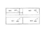
図11は、従来のDDR(Double Data Rate)−SDRAM(Synchronous Dynamic Random Accesses Memory)の全体構成を示すレイアウト図である。図11を参照して、このSDRAMは4個のバンクBNK0〜BNK3から構成され、16ビットのデータを入出力し、256Mビットの記憶容量を有する。
【0003】
各バンクBNKi(i=0〜3)は、8K個のワード線(図示せず)と、8K個のビット線対(図示せず)と、8K個のセンスアンプ(図示せず)とを含み、64Mビットの記憶容量を有する。各バンクBNKiは16ビットのデータを入出力する。
【0004】
各バンクBNKiは、16個のアレイに分割される。図11では、バンクBNK0のアレイARY2及びARY3と、バンクBNK1のアレイARY1が代表的に示される。各アレイは、512個のワード線と、8K個のビット線対と、8K個のセンスアンプとを含み、4Mビットの記憶容量を有する。各アレイは、16ビットのデータを入出力する。
【0005】
このSDRAMは、あるバースト動作を途中で中止して別のバースト動作を開始するバースト割込機能を有する。このバースト割込機能を図12のタイミング図を参照して説明する。ここでは、CAS(Column Address Strobe)レイテンシ(Latency)を「2クロック」、バースト長を「8ビット」とし、バースト読出動作を説明する。このSDRAMはDDR型であるから、8ビットのバーストデータを2ビットごとに別の8ビットのバーストデータに置き換えることができる。具体的には、3ビット目、5ビット目、又は7ビット目以降のバーストデータを別のバーストデータに置き換えることができる。
【0006】
まず、コマンドRAS1が与えられる。このコマンドRAS1は、RAS(Row Address Strobe)に応答してロウアドレスを入力することを意味する。コマンドRAS1により入力されたロウアドレスに応答して、バンクBNK1が活性化され、そのバンクBNK1内のアレイARY1が活性化される。ここでは、バンクBNK1内のアレイARY1が活性化される前に、既にバンクBNK0が活性化され、そのバンクBNK0内のアレイARY2が活性化されている。
【0007】
続いて、コマンドR1CAS1が与えられる。このコマンドR1CAS1は、CASに応答してカラムアドレスを入力することを意味する。コマンドR1CAS1から2クロック後にバースト読出動作が始まる。具体的には、活性化されたバンクBNK1内のアレイARY1のうち、コマンドR1CAS1により入力されたカラムアドレスから連続してデータが読み出される。
【0008】
続いて、コマンドR1CAS1から2クロック後にコマンドR2CAS1が与えられると、このコマンドR2CAS1から2クロック後に別のバースト読出動作が始まる。具体的には、別のバンクBNK0内のアレイARY2のうち、コマンドR2CAS1により入力されたカラムアドレスから連続してデータが読み出される。
【0009】
このとき、コマンドR1CAS1に応答して始まったバースト読出動作は、コマンドR2CAS1に応答して始まったバースト読出動作により割り込まれる。具体的には、コマンドR1CAS1に応答して始まったバースト読出動作は、4ビット目のデータが読み出された後に中止され、5ビット目以降のデータは、コマンドR2CAS1に応答して始まったバースト読出動作により読み出されるデータで置き換えられる。
【0010】
続いて、コマンドR2CAS1から2クロック後にコマンドR2CAS2が与えられると、このコマンドR2CAS2から2クロック後にさらに別のバースト読出動作が始まる。具体的には、同じバンクBNK0内の同じアレイARY2のうち、コマンドR2CAS2により入力された別のカラムアドレスから連続してデータが読み出される。
【0011】
このとき、コマンドR2CAS1に応答して始まったバースト読出動作は、コマンドR2CAS2に応答して始まったバースト読出動作により割り込まれる。具体的には、コマンドR2CAS1に応答して始まったバースト読出動作は、4ビット目のデータが読み出された後に中止され、5ビット目以降のデータは、コマンドR2CAS2に応答して始まったバースト読出動作により読み出される8ビットのデータで置き換えられる。
【0012】
以上のように、従来のSDRAMは、バースト読出動作に割り込みが生じた場合でも、割り込みで入力される新しいアドレスが既に活性化されている別のバンク内のカラムアドレスか、又は現在活性化されている同じバンク内の同じアレイ内の別のカラムアドレスであれば、データをシームレスに出力することができる。しかし、これら以外のカラムアドレスであれば、データをシームレスに出力することはできない。
【0013】
たとえば同じバンクBNK0内であってもアレイARY2から別のアレイARY3にアドレスが移行する場合は、まずアレイARY2がコマンドPRC1に応答してプリチャージされて不活性化され、改めてアレイARY3がコマンドRAS3に応答して活性化されなければならない。この場合、コマンドR3CAS3から2クロック後にようやく8ビットのバースト読出動作が始まる。そのため、出力されるバーストデータに8ビット分の空きが生じ、データレートが低下する。
【0014】
上記のようなバースト読出動作の割り込みは、あるコンピュータプログラムの実行中にもっと優先順位の高い別のコンピュータプログラムが実行される場合に起きる。この場合、割り込みで入力される新しいアドレスが同じロウアドレス内のカラムアドレスであることはほとんどない。したがって、従来のSDRAMはバースト割込機能を備えていても、ほとんど有効に活用できていない。
【0015】
図11に示したSDRAMの場合、16個のアレイのうち1個が選択され、その選択されたアレイ内で1個のワード線が活性化されると、8K個のセンスアンプが活性化される。このSDRAMは16個の入出力を備えているため、1個の入出力当たりのページ長は512(=8K÷16)ビットである。すなわち、シームレスに割り込みを処理できるアドレスは512個しかない。仮に4個のバンクBNK0〜BNK3全てが活性化されていたとしても、シームレスに割り込みを処理できるアドレスは2K(=512×4)個しかない。これは、1個の入出力当たりの全アドレス数である16M(=256M÷16)に比べると非常に少ない。シームレスに割り込みを処理できる確率はこれらのアドレス空間比(2K/16M)で決定され、わずか0.012%でしかない。すなわち、バースト動作割り込み要求のうちの99.998%はシームレスに実行できないことになる。よって、ほとんどの場合、出力されるバーストデータに空きが生じ、データレートが低下してしまう。
【0016】
上記ではバースト割込機能にある問題をバースト読出動作を例に挙げて説明したが、同様の問題はバースト書込動作でも起きる。
【0017】
なお、特開2000−195253号公報(米国特許第6252794号)は、バースト長に対応する数のセンスアンプだけを活性化することによりバースト動作間の空き時間を短くしたSDRAMを開示しているが、バースト動作の割り込みについては全く言及していない。
【0018】
【発明が解決しようとする課題】
本発明の1つの目的は、バースト動作中に割り込みが入ってもシームレスなデータの入出力が可能な半導体記憶装置を提供することである。
【0019】
本発明のもう1つの目的は、バースト動作を途中で切り換える有効な割り込みが起きる確率を高くした半導体記憶装置を提供することである。
【0024】
【課題を解決するための手段】
本発明による半導体記憶装置は、複数のセグメントアレイと、複数のセグメント制御回路とを備える。セグメントアレイの各々は、複数のユニットアレイと、複数のユニットアレイを縦断する複数のカラム選択線とを含む。複数のセグメント制御回路は、複数のセグメントアレイに対応して設けられる。複数のユニットアレイは互いに独立して動作する。ユニットアレイの各々は、複数のワード線と、ラッチ手段と、ロウデコーダとを含む。ラッチ手段は、ロウプリデコード信号をラッチする。ロウデコーダは、ラッチ手段にラッチされたロウプリデコード信号に応答して複数のワード線を選択的に駆動することによりデータを読み出す。セグメント制御回路の各々は、セグメント選択回路と、ユニットアレイ選択回路と、ロウプリデコーダと、カラム選択線ドライバと、第1のプリフェッチラッチ回路とを含む。セグメント選択回路は、対応するセグメントアレイを活性化する。ユニットアレイ選択回路は、対応するセグメントアレイに含まれる複数のユニットアレイを選択的に活性化する。ロウプリデコーダは、ロウアドレス信号をプリデコードしてロウプリデコード信号を出力する。カラム選択線ドライバは、カラムアドレス信号に応答して複数のカラム選択線を選択的に駆動することによりロウデコーダにより読み出されたデータのうち複数ビットのデータを選択する。第1のプリフェッチラッチ回路は、ユニットアレイ選択回路により活性化されたユニットアレイから読み出されかつカラム選択線ドライバにより選択された複数ビットのデータをラッチする。
【0025】
この半導体記憶装置では、セグメントアレイは互いに独立して活性化されるので、活性化された1つのセグメントアレイ内のユニットアレイから複数ビットのデータが連続的に読み出されている間に割り込みが入り、活性化されたもう1つのセグメントアレイから複数ビットのデータが連続的に読み出され得る。そのため、シームレスなバーストデータの出力が可能になる。
【0027】
好ましくは、セグメント制御回路の各々はさらに、第2のプリフェッチラッチ回路を含む。第2のプリフェッチラッチ回路は、ユニットアレイ選択回路により活性化されたもう1つのユニットアレイから読み出されかつカラム選択線ドライバにより選択された複数ビットのデータをラッチする。
【0028】
この場合、活性化された1つのユニットアレイから読み出された複数ビットのデータは第1のプリフェッチラッチ回路にラッチされ、活性化されたもう1つのユニットアレイから読み出された複数ビットのデータは第2のプリフェッチラッチ回路にラッチされる。したがって、1つのセグメントアレイ内のユニットアレイ間でもバースト読出動作の割り込みが可能である。
【0031】
好ましくは、セグメント制御回路の各々はさらに、第1のプリロードラッチ回路を含む。第1のプリロードラッチ回路は、ユニットアレイ選択回路により活性化されたユニットアレイに書き込まれかつカラム選択線ドライバにより選択されるべき複数ビットのデータをラッチする。
【0032】
好ましくは、セグメント制御回路の各々はさらに、第1のプリロードラッチ回路にラッチされた複数ビットのデータを部分的にマスクするマスク手段を含む。
【0033】
この場合、当該ユニットアレイのバースト書込動作中に割り込みが入り、割り込み後に第1のプリロードラッチ回路にラッチされたデータは、当該他のユニットアレイに書き込まれるべきでデータあるから、マスク手段によりマスクされ、当該ユニットアレイには書き込まれない。
【0034】
好ましくは、セグメント制御回路の各々はさらに、第2のプリロードラッチ回路を含む。第2のプリロードラッチ回路は、ユニットアレイ選択回路により活性化されたもう1つのユニットアレイに書き込まれかつカラム選択線ドライバにより選択されるべき複数ビットのデータをラッチする。
【0035】
この場合、活性化された1つのユニットアレイに書き込まれた複数ビットのデータは第1のプリロードラッチ回路にラッチされ、活性化されたもう1つのユニットアレイに書き込まれた複数ビットのデータは第2のプリロードラッチ回路にラッチされる。したがって、1つのセグメントアレイ内のユニットアレイ間でもバースト書込動作の割り込みが可能である。
【0036】
【発明の実施の形態】
以下、本発明の実施の形態を図面を参照して詳しく説明する。図中同一又は相当部分には同一符号を付してその説明を援用する。
【0037】
[第1の実施の形態]
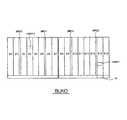
図1を参照して、本発明の第1の実施の形態によるDDR−SDRAMは、4個のブロックBLK0〜BLK3から構成される。各ブロックBLKi(i=0〜3)は、64Mビットの記憶容量を有する。
【0038】
また、各ブロックBLKiに対応して4個の入出力パッド(図3中のIO)が設けられる。よって、このSDRAM全体は16個の入出力パッドを備える。各ブロックBLKiは、対応する4個の入出力パッドを通じて4ビットのデータを入出力する。よって、このSDRAM全体は16ビットのデータを入出力する。
【0039】
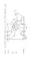
図2は、ブロックBLK0の構成を示すレイアウト図である。他のブロックBLK1〜BLK3の構成はブロックBLK0の構成と基本的に同じであるから、以下ではブロックBLK0の構成を代表的に説明する。
【0040】
図2を参照して、ブロックBLK0は、16個のセグメントアレイ#0〜#15と、4個のメインロウデコーダMRD0〜MRD3とを含む。メインロウデコーダMRD0は、セグメントアレイ#1及び#2の間に配置され、4個のセグメントアレイ#0〜#3により共有される。メインロウデコーダMRD1は、セグメントアレイ#5及び#6の間に配置され、4個のセグメントアレイ#4〜#7により共有される。メインロウデコーダMRD2は、セグメントアレイ#9及び#10の間に配置され、4個のセグメントアレイ#8〜#11により共有される。メインロウデコーダMRD3は、セグメントアレイ#13及び#14の間に配置され、4個のセグメントアレイ#12〜#15により共有される。
【0041】
ブロックBLK0はさらに、16個のセグメントアレイ#0〜#15に対応する16個のセグメント制御回路を含む。図2では、セグメントアレイ#14に対応する1個のセグメント制御回路10が代表的に示されている。各セグメント制御回路は、対応するセグメントアレイを制御する。
【0042】
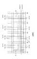
図3は、セグメントアレイ#14及びセグメント制御回路10の構成を示す機能ブロック図である。以下ではセグメントアレイ#14及びセグメント制御回路10の構成を代表的に説明する。
【0043】
図3を参照して、セグメントアレイ#14は、16個のユニットアレイを含む。図3では、1個のユニットアレイUARYが代表的に示されている。各ユニットアレイUARYは、256Kビットの記憶容量を有する。各ユニットアレイUARYは、4個のサブアレイSARYに分割される。
【0044】
セグメント制御回路10は、カラム選択線ドライバ12と、カラムアドレスマスク回路14と、32(=8×4)個のグローバルデータ線対GDLと、4個のプリフェッチラッチ回路PFLと、4個のプリロードラッチ回路PLLとを含む。各サブアレイSARYに対応して8個のグローバルデータ線対GDLが設けられる。各プリフェッチラッチ回路PFLは、対応するサブアレイSARYから8個のグローバルデータ線対GDLを通じて読み出された8ビットのデータを読出イネーブル信号REに応答してラッチする。各プリロードラッチ回路PLLは、8個のグローバルデータ線対GDLを通じて対応するサブアレイSARYに書き込まれるべき8ビットのデータを書込イネーブル信号WEに応答してラッチする。
【0045】
セグメントアレイ#14を含むブロックBLK0はさらに、16個のセグメントアレイ#0〜#15に共通に設けられた4個の読出データバスRDBと、16個のセグメントアレイ#0〜#15に共通に設けられた4個の書込データバスWDBと、4個の入出力パッドIOとを含む。
【0046】
各セグメント制御回路10内の4個のプリフェッチラッチ回路PFLは、4個の読出データバスRDBにそれぞれ接続される。各セグメント制御回路10内の4個のプリロードラッチ回路PLLは、4個の書込データバスWDBにそれぞれ接続される。各入出力パッドIOは、対応する1個の読出データバスRDBと、対応する1個の書込データバスWDBとに接続される。
【0047】
各読出データバスRDBは、対応するプリフェッチラッチ回路PFLから与えられた読出データを2ビットずつ対応する入出力パッドIOに伝送する。各書込データバスWDBは、対応する入出力パッドIOから与えられた書込データを2ビットずつ対応するプリロードラッチ回路PLLに伝送する。
【0048】
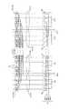
図4は、各ユニットアレイUARYの構成を示すレイアウト図である。図4を参照して、各ユニットアレイUARYは、いわゆる階層ワード線構成を有する。
【0049】
具体的には、各サブアレイSARYは、行に配置された512個のセグメントワード線(単に「ワード線」ともいう。)WLと、64個のセグメントロウデコーダSRDとを含む。各セグメントロウデコーダSRDは、8個のセグメントワード線WLに対応して設けられ、それら対応するセグメントワード線WLを選択的に駆動する。セグメントワード線WLはポリサイドからなり、メモリセルトランジスタ(図示せず)のゲート電極を形成する。
【0050】
各サブアレイSARYはさらに、列に配置された128個のビット線対BLと、それらビット線対BLにそれぞれ接続された128個のセンスアンプSAとを含む。128個のセンスアンプSAは、それらビット線対BLの両側に64個ずつ配置される。よって、ユニットアレイUARY全体は、512個のビット線対BLと、512個のセンスアンプSAとを含む。ビット線対BLは、セグメントワード線WLのポリサイド層よりも下の金属層に形成される。
【0051】
ユニットアレイUARYには、128個のメインワード線MWLが横断する。このうち64個のメインワード線MWL(#14)はこのユニットアレイUARYのセグメントロウデコーダSRDに接続されるが、残り64個のメインワード線MWL(#15)は隣接セグメントアレイ#15内のユニットアレイのセグメントロウデコーダに接続される。メインワード線MWLはメインロウデコーダMRD3の両側から延び出し、図上右側のセグメントアレイ#14及び#15を横断するとともに、図上左側のセグメントアレイ#13及び#12を横断する。メインロウデコーダMRD3は、セグメントアレイ#12〜#15内のメインワード線MWLをロウアドレス信号に応答して選択的に駆動する。メインワード線MWLは、セグメントワード線WLのポリサイド層よりも上の第1の金属層に形成される。
【0052】
各サブアレイSARYには、64個のカラム選択線CSLが縦断する。よって、ユニットアレイUARY全体には、256個のカラム選択線CSLが縦断する。256個のカラム選択線CSLは、カラム選択線ドライバ12に接続される。カラム選択線ドライバ12は、256個のカラム選択線CSLをカラムアドレス信号に応答して選択的に駆動する。カラム選択線CSLは、第1の金属層よりも上の第2の金属層に形成される。
【0053】
各サブアレイSARYにはまた、8個のグローバルデータ線対GDLが縦断する。よって、ユニットアレイUARY全体には、32個のグローバルデータ線対GDLが縦断する。各サブアレイSARYを縦断する8個のグローバルデータ線対GDLは、対応するプリフェッチラッチ回路PFL及びプリロードラッチ回路PLLに接続される。グローバルデータ線対GDLもまた、第2の金属層に形成される。
【0054】
図5は、セグメント制御回路10の構成を示す機能ブロック図である。図5を参照して、セグメント制御回路10は、上述したプリフェッチラッチ回路PFL及びプリロードラッチ回路PLLの他に、セグメント選択回路16と、ユニットアレイ選択回路18と、ロウプリデコーダ20と、ANDゲートG1及びG2とを含む。
【0055】
このSDRAMは16Mビット×16構成であり、24(16M=224)ビットのグローバルアドレス信号GAを受ける。グローバルアドレス信号GAは、4ビットのセグメント選択アドレス信号SSAと、4ビットのユニットアレイ選択アドレス信号UASAと、16ビットのロウ/カラムアドレス信号RCAとからなる。
【0056】
セグメント選択アドレス信号SSAは、16個のセグメントアレイ#0〜#15のうち1個を選択するためのアドレス信号である。ユニットアレイ選択アドレス信号UASAは、選択された1個のセグメントアレイ内において16個のユニットアレイUARYのうち1個を選択するためのアドレス信号である。ロウ/カラムアドレス信号RCAは、選択されたユニットアレイUARYのロウ及びカラムを選択するためのアドレス信号である。
【0057】
セグメント選択回路16は、セグメント選択アドレス信号SSAに応答してセグメント選択信号SSをH(論理ハイ)レベルに活性化する。セグメント選択信号SSは、ANDゲートG1,G2及びユニットアレイ選択回路18に与えられる。セグメント選択信号SSが活性化されると、読出時には、読出イネーブル信号REがHレベルに活性化され、プリフェッチラッチ回路PFLに与えられ、また書込時には、書込イネーブル信号WEがHレベルに活性化され、プリロードラッチ回路PLLに与えられる。
【0058】
また、セグメント選択信号SSが活性化されると、ユニットアレイ選択回路18が活性化される。ユニットアレイ選択回路18は、活性化されると、ユニットアレイ選択アドレス信号UASAに応答して16個のユニットアレイイネーブル信号UAEのうち1個を活性化する。
【0059】
ロウプリデコーダ20は、ロウ/カラムアドレス信号RCAに含まれるロウアドレス信号をプリデコードしてグローバルロウプリデコード信号GRPを出力する。グローバルロウプリデコード信号GRPは、セグメントアレイ#14内の全ユニットアレイUARYを縦断する複数のグローバルロウプリデコード線GRPLに与えられる。
【0060】
図6は、各ユニットアレイUARYにおけるセグメントロウデコーダSRD周辺の構成を示す機能ブロック図である。図6を参照して、各ユニットアレイUARYは、上述した256個のセグメントロウデコーダSRDの他に、アレイタイミング制御回路22と、複数のANDゲートG3と、複数のラッチ回路24と、複数のローカルロウプリデコード線LRPLとを含む。
【0061】
アレイタイミング制御回路22は、対応するユニットアレイイネーブル信号UAEがHレベルに活性化されると活性化され、このユニットアレイUARYの動作を制御する。ANDゲートG3は、対応するユニットアレイイネーブル信号UAEがHレベルに活性化されると、グローバルロウプリデコード信号GRPをラッチ回路24に与える。ラッチ回路24は、グローバルロウプリデコード信号GRPをラッチし、これらをローカルロウプリデコード信号LRPとしてローカルロウプリデコード線LRPLに与える。ローカルロウプリデコード線LRPLは、このユニットアレイUARY内のセグメントロウデコーダSRDに接続される。よって、セグメントロウデコーダSRDは、ローカルロウプリデコード信号LRPに応答してセグメントワード線WLを選択的に活性化する。
【0062】
次に、このような構成を有するSDRAMのバースト読出動作を図7のタイミング図を参照して説明する。
【0063】
まず、コマンドR1A1が与えられ、グローバルアドレス信号GAが入力される。このコマンドR1A1により入力されたグローバルアドレス信号GAは、セグメントアレイ#14を選択するためのセグメントアレイアドレス信号SSAと、セグメントアレイ#14内のユニットアレイUARY1(図2参照)を選択するためのユニットアレイ選択アドレス信号UASAと、ユニットアレイUARY1内のロウ及びカラムを選択するためのロウ/カラムアドレス信号RCAとを含む。
【0064】
セグメント選択回路16は、セグメント選択アドレス信号SSAに応答してセグメント選択信号SSをHレベルに活性化する。セグメント選択信号SSがHレベルに活性化されると、ユニットアレイ選択回路18は、ユニットアレイ選択アドレス信号UASAに応答して、ユニットアレイUARY1を活性化するためのユニットアレイイネーブル信号UAEをHレベルに活性化する。また、セグメント選択信号SSがHレベルに活性化されると、読出時においては、ANDゲートG1から出力される読出イネーブル信号REがHレベルに活性化される。読出イネーブル信号REが活性化されると、セグメント制御回路10内の8個のプリフェッチラッチ回路PFLが活性化される。
【0065】
ロウ/カラムアドレス信号RCAに含まれるロウアドレス信号は、ロウプリデコーダ20によりプリデコードされ、グローバルロウプリデコード信号GRPが生成される。このグローバルロウプリデコード信号GRPは、グローバルロウプリデコード線GRPLに与えられる。
【0066】
ユニットアレイUARY1においては、活性化されたユニットアレイイネーブル信号UAEに応答して、アレイタイミング制御回路22が活性化され、かつグローバルロウプリデコード信号GRPがラッチ回路24にラッチされる。ラッチされたグローバルロウプリデコード信号GRPはローカルロウプリデコード信号LRPとしてセグメントロウデコーダSRDに与えられ、これによりセグメントワード線WLが選択的に活性化される。
【0067】
続いて、ユニットアレイUARY1において、全センスアンプSAが活性化され、さらにカラム選択線ドライバ12により全カラム選択線CSLのうち32個のカラム選択線CSLが活性化される。すなわち、各サブアレイSARYごとに8個のカラム選択線CSLが活性化される。これにより、各サブアレイSARYから同時に読み出された8ビットのデータは8個のグローバルデータ線対GDLを通じて対応する1個のプリフェッチラッチ回路PFLに伝送され、ラッチされる。したがって、4個のサブアレイSARYからなるユニットアレイUARY1全体からは32ビットのデータが同時に読み出され、4個のプリフェッチラッチ回路PFLにラッチされる。
【0068】
各プリフェッチラッチ回路PFLからデータが2ビットずつ読出データバスRDBを通じて伝送され始め、対応する入出力パッドIOから8ビットのバーストデータが出力され始める。
【0069】
上記のように、グローバルロウプリデコード信号GRPはユニットアレイUARY1内のラッチ回路24にラッチされるため、ユニットアレイUARY1はグローバルアドレス信号GAから切り離され、他のユニットアレイから独立した動作が可能になる。ユニットアレイUARY1が他のユニットアレイから独立して動作するために、アレイタイミング制御回路22は、ワード線WLの活性化、センスアンプSAの活性化、メモリセルデータの再書込、ワード線WLの不活性化、ビット線対BLのプリチャージといった一連の動作を自己完結的に制御する。
【0070】
アレイタイミング制御回路22は、ビット線対BLのプリチャージを完了すると、リセット信号RSTをラッチ回路24に与える。これによりグローバルアドレス信号GAからの離隔が解除され、ユニットアレイイネーブル信号UAEが再び活性化されれば、ユニットアレイUARY1は再び選択される。
【0071】
上記のように、ユニットアレイUARY1は他のユニットアレイから独立して動作するため、ユニットアレイUARY1の動作が完了する前に、次のグローバルアドレス信号GAを与えることができる。
【0072】
コマンドR1A1の2クロック後にコマンドR2A1が与えられると、このコマンドR2A1により別のセグメントアレイ#3のユニットアレイUARY2(図2参照)が選択される。ユニットアレイUARY2はユニットアレイUARY1から2クロックだけ遅れて動作するが、ユニットアレイUARY1及びUARY2は相互に独立して動作する。
【0073】
ユニットアレイUARY2もユニットアレイUARY1と同様に動作するため、ユニットアレイUARY2からも8ビットのバーストデータが出力され始める。ユニットアレイUARY2を含むセグメントアレイ#3が選択されたときには、セグメントアレイ#14の読出イネーブル信号REは不活性化される。そのため、セグメントアレイ#14のプリフェッチラッチ回路PFLは不活性化され、ユニットアレイUARY1からの5ビット目以降のバーストデータは出力されない。その代わり、ユニットアレイUARY2からのバーストデータが出力される。
【0074】
コマンドR2A1から2クロック後にユニットアレイUARY1は動作を完了するが、コマンドR1A2により再び動作を開始する。したがって、コマンドR2A1に応答して始まったバースト読出動作は4ビット目のデータ出力後に割り込みにより中止され、その代わりコマンドR1A2に応答したバースト読出動作が始まる。
【0075】
コマンドR1A2の入力から4クロック後にコマンドR1A3が与えられると、ユニットアレイUARY1は動作を一旦完了した後に再び開始するので、コマンドR1A2による8ビットのバーストデータが出力された後、直ちにコマンドR1A3による8ビットのバーストデータが出力される。
【0076】
図8は、カラムアドレスマスク回路14及びその周辺の構成を部分的に示す回路図である。図8では、1個のサブアレイSARYに対応する部分のみが示されている。また、ビット線対BL、グローバルデータ線対GDL0〜GDL7は、2本で1対をなすが、1本の線で示されている。また、ビットスイッチ(カラム選択ゲート)CSGも、2個で1対をなすが、1個のトランスファーゲートで示されている。
【0077】
各サブアレイSARYは、128個のビット線対BLに対応して128個のビットスイッチCSGを含む。このSDRAMはDDR型であるから、カラム選択線CSLは2個のビットスイッチCSGに対応して1個ずつ設けられる。すなわち、8個のビットスイッチCSGに対応して4個のカラム選択線CSLが設けられる。よって、図4にも示したように、各サブアレイSARY全体には64(=4×16)個のカラム選択線CSLが縦断し、さらに8個のグローバルデータ線対GDL0〜GDL7が縦断する。
【0078】
カラムアドレスマスク回路14は、複数のカラム選択線CSLに対応する複数のANDゲートG4を含む。ユニットアレイUARY全体には256個のカラム選択線CSLが縦断しているため、カラムアドレスマスク回路14全体は256個のANDゲートG4を含む。
【0079】
各サブアレイは、16ビットのカラム選択信号CS0〜CS15を受ける。カラム選択信号CS0〜CS15は、カラム選択線ドライバ12により生成される。カラム選択信号CS0〜CS15の各々は、対応する4個のANDゲートG4に与えられる。これら4個のANDゲートG4には、それぞれマスク信号MSK0〜MSK3が与えられる。マスク信号MSK0〜MSK3は、バースト読出時には全てHレベルになる。一方、8ビットデータのバースト書込時において、3ビット目に割り込みが入る場合にはマスク信号MSK0はHレベルになり、マスク信号MSK1〜MSK3はLレベルになる。5ビット目に割り込みが入る場合にはマスク信号MSK0及びMSK1はHレベルになり、マスク信号MSK2及びMSK3はLレベルになる。7ビット目に割り込みが入る場合にはマスク信号MSK0〜MSK2はHレベルになり、マスク信号MSK3はLレベルになる。
【0080】
次に、このSDRAMのバースト書込動作を図9のタイミング図を参照して説明する。
【0081】
図9に示したバースト書込の場合も図7に示したバースト読出の場合と同じタイミングで、コマンドR1A1、R2A1、R1A2、及びR1A3が与えられる。ただし、バースト書込の場合には、各コマンドと同時にバーストデータが入力され始める。
【0082】
コマンドR1A1から2クロック後にコマンドR2A1が与えられるので、コマンドR1A1に応答して前半4ビットのデータは入力されるが、後半4ビットのデータは入力されない。その代わり、コマンドR2A1に応答して前半4ビットのデータが入力される。また、コマンドR2A1から2クロック後にコマンドR1A2が与えられるので、コマンドR2A1に応答して前半4ビットのデータは入力されるが、後半4ビットのデータは入力されない。その代わり、コマンドR1A2に応答して前半4ビットのデータが入力される。コマンドR1A2から4クロック後にコマンドR1A3が与えられるので、コマンドR1A2に応答して8ビットのデータは全て入力される。
【0083】
コマンドR1A1が与えられると、上述したバースト読出時と同様に、セグメントアレイ#14が選択され、さらにセグメントアレイ#14内のユニットアレイUARY1が選択される。ただし、上述したバースト読出時と異なり、書込イネーブル信号WEがHレベルに活性化され、プリロードラッチ回路PLLが活性化される。したがって、コマンドR1A1に応答して入力された前半4ビットのデータと、コマンドR2A1に応答して入力された前半4ビットのデータとは、対応する書込データバスWDBを通じて2ビットずつ伝送され、対応するプリロードラッチ回路PLLにラッチされる。
【0084】
プリロードラッチ回路PLLにラッチされた8ビットのデータは、タイミングT1で対応する8個のグローバルデータ線対GDLを通じてユニットアレイUARY1に向けて伝送される。しかし、この場合は、2クロック後に次のコマンドが与えられているため、マスク信号MSK0及びMSK1はHレベルになるが、マスク信号MSK2及びMSK3はLレベルになる。そのため、伝送された8ビットのデータのうち前半4ビットのデータはユニットアレイUARY1に書き込まれるが、後半4ビットのデータはカラムアドレスマスク回路14によりマスクされ、ユニットアレイUARY1には書き込まれない。
【0085】
コマンドR1A1から2クロック後にコマンドR2A1が与えられるので、セグメントアレイ#3が選択され、さらにそのセグメントアレイ#3内のユニットアレイUARY2が選択される。したがって、コマンドR2A1に応答して入力された前半4ビットのデータは、セグメントアレイ#3に対応するプリロードラッチ回路PLLにもラッチされる。コマンドR2A1から2クロック後にコマンドR1A2が与えられるので、コマンドR1A2に応答して入力された前半4ビットのデータもまたこのプリロードラッチ回路PLLにラッチされる。このプリロードラッチ回路PLLにラッチされた8ビットのデータは、タイミングT2で対応する8個のグローバルデータ線対GDLを通じてユニットアレイUARY2に向けて伝送されるが、コマンドR2A1により入力された前半4ビットのデータのみがユニットアレイUARY2に書き込まれ、後半4ビットのデータはマスクされ、ユニットアレイUARY2には書き込まれない。この後半4ビットのデータは、後述するタイミングT3でセグメントアレイ#14のユニットアレイUARY1に書き込まれる。
【0086】
コマンドR1A2によるバースト書込動作には割り込みが入らないので、コマンドR1A2により入力された8ビットのデータは全て、タイミングT3でセグメントアレイ#14のユニットアレイUARY1に書き込まれる。
【0087】
以上のように、本発明の第1の実施の形態によれば、セグメントアレイ#0〜#15が互いに独立して活性化されるので、あるセグメントアレイ内のあるユニットアレイUARYのバースト動作が割り込まれ、既に活性化されている別のセグメントアレイ内の任意のユニットアレイのバースト動作が直ちに開始される。したがって、シームレスなバーストデータの入出力が可能になる。この第1の実施の形態では、そのような有効な割り込みが起きる確率は93.75%(=15÷16)と、従来の0.012%に比べて飛躍的に高くなる。
【0088】
[第2の実施の形態]
上記第1の実施の形態ではセグメントアレイ間のバースト割込は可能であるが、同じセグメントアレイ内におけるユニットアレイ間のバースト割込は不可能である。したがって、有効な割り込みが起きる確率をさらに高くするためには、セグメントアレイ単位だけでなく、ユニットアレイ単位でも独立したバースト動作を可能にすればよい。
【0089】
具体的には、上記第1の実施の形態では、各セグメントアレイに対応して4個のプリフェッチラッチ回路PFL及び4個のプリロードラッチ回路PLLが設けられているのに対し、この第2の実施の形態では、図10に示すように、8個のプリフェッチラッチ回路PFLA,PFLB及び8個のプリロードラッチ回路PLLA,PLLBが設けられる。すなわち、各サブアレイSARYに対応して2個のプリフェッチラッチ回路PFLA,PFLB及び2個のプリロードラッチ回路PLLA,PLLBが設けられる。
【0090】
また、ユニットアレイ選択回路18により選択されたユニットアレイUARY内のビットスイッチCSGのみが動作するように、カラム選択信号CSがそのユニットアレイ内で活性化されるようにする。より具体的には、各ビットスイッチCSGと直列にもう1つトランスファーゲートを接続し、このトランスファーゲートを各ユニットアレイUARYごとに対応するユニットアレイイネーブル信号UAEに応答してオン・オフさせればよい。
【0091】
この第2の実施の形態によれば、各サブアレイSARYに対応して2個のプリフェッチラッチ回路PFLA,PFLB及び2個のプリロードラッチ回路PLLA,PLLBが設けられているため、8ビットのバースト動作中に2回まで割り込みが可能になる。バースト読出動作の場合は、1回目の割り込み前の8ビットのバーストデータはプリフェッチラッチ回路PFLAにラッチされ、2回目の割り込み前の8ビットのバーストデータはプリフェッチラッチ回路PFLBにラッチされる。一方、バースト書込動作の場合は、1回目の割り込み前の8ビットのバーストデータはプリロードラッチ回路PLLAにラッチされ、2回目の割り込み前の8ビットのバーストデータはプリロードラッチ回路PLLBにラッチされる。
【0092】
また、各ユニットアレイUARYが独立してバースト動作を行うため、セグメントアレイ間だけでなく、同じセグメントアレイ内におけるユニットアレイ間でもバースト割込が可能になる。すなわち、256(=16×16)個のユニットアレイUARYのうちバースト割込が不可能なのは現在バースト動作中の1個のユニットアレイUARY内だけで、他の255個のユニットアレイでは可能である。したがって、有効な割り込みが起きる確率は99.6%(=255÷256)と、上記第1の実施の形態よりも高くなる。
【0093】
[他の実施の形態]
上記第2の実施の形態ではプリフェッチラッチ回路PFLA,PFLB及びプリロードラッチ回路PLLA,PLLBを2個ずつ設けているが、8ビットのバースト動作中に2ビットごと4回までの割り込みを可能にするためには、プリフェッチラッチ回路及びプリロードラッチ回路を4個ずつ設ければよい。
【0094】
また、本発明は、DDR−SDRAMに限定されることなく、通常のSDR(Single Data Rate)型のSDRAM、非同期型DRAM、SRAM(Static Random Accesses Memory)、ROM(Read Only Memory)にも適用可能である。
【0095】
以上、本発明の実施の形態を説明したが、上述した実施の形態は本発明を実施するための例示に過ぎない。よって、本発明は上述した実施の形態に限定されることなく、その趣旨を逸脱しない範囲内で上述した実施の形態を適宜変形して実施することが可能である。
【図面の簡単な説明】
【図1】本発明の第1の実施の形態によるDDR−SDRAMの全体構成を示すレイアウト図である。
【図2】図1中の各ブロックの構成を示すレイアウト図である。
【図3】図2中の各セグメントアレイ、セグメント制御回路及びその周辺の構成を示す機能ブロック図である。
【図4】図3中の各ユニットアレイの構成を示すレイアウト図である。
【図5】図2中のセグメント制御回路の構成を示す機能ブロック図である。
【図6】図4中のユニットアレイにおけるセグメントロウデコーダ周辺の構成を示す機能ブロック図である。
【図7】図1に示したSDRAMのバースト読出動作を示すタイミング図である。
【図8】図3中のカラムアドレスマスク回路及びその周辺の構成を部分的に示す回路図である。
【図9】図1に示したSDRAMのバースト書込動作を示すタイミング図である。
【図10】本発明の第2の実施の形態によるSDRAMにおける各セグメントアレイ、セグメント制御回路及びその周辺の構成を示す機能ブロック図である。
【図11】従来のSDRAMの全体構成を示すレイアウト図である。
【図12】図11に示した従来のSDRAMのバースト読出動作を示すタイミング図である。
【符号の説明】
10 セグメント制御回路
12 カラム選択線ドライバ
14 カラムアドレスマスク回路
16 セグメント選択回路
18 ユニットアレイ選択回路
BLK0〜BLK3 ブロック
#0〜#15 セグメントアレイ
UARY,UARY1,UARY2 ユニットアレイ
PFL,PFLA,PFLB プリフェッチラッチ回路
PLL,PLLA,PLLB プリロードラッチ回路
RE 読出イネーブル信号
WE 書込イネーブル信号[0001]
BACKGROUND OF THE INVENTION
The present invention relates to a semiconductor memory device, and more particularly to a semiconductor memory device having a burst interrupt function for switching a burst operation halfway.
[0002]
[Prior art]
FIG. 11 is a layout diagram showing the overall structure of a conventional DDR (Double Data Rate) -SDRAM (Synchronous Dynamic Random Access Memory). Referring to FIG. 11, the SDRAM is composed of four banks BNK0 to BNK3, and inputs / outputs 16-bit data and has a storage capacity of 256 Mbits.
[0003]
Each bank BNKi (i = 0-3) includes 8K word lines (not shown), 8K bit line pairs (not shown), and 8K sense amplifiers (not shown). , And has a storage capacity of 64 Mbits. Each bank BNKi inputs / outputs 16-bit data.
[0004]
Each bank BNKi is divided into 16 arrays. In FIG. 11, arrays ARY2 and ARY3 of bank BNK0 and array ARY1 of bank BNK1 are representatively shown. Each array includes 512 word lines, 8K bit line pairs, and 8K sense amplifiers, and has a storage capacity of 4M bits. Each array inputs and outputs 16-bit data.
[0005]
This SDRAM has a burst interrupt function for stopping a certain burst operation halfway and starting another burst operation. This burst interrupt function will be described with reference to the timing chart of FIG. Here, a burst reading operation will be described with a CAS (Column Address Strobe) latency of “2 clocks” and a burst length of “8 bits”. Since this SDRAM is a DDR type, 8-bit burst data can be replaced with another 8-bit burst data every two bits. Specifically, the burst data after the third bit, the fifth bit, or the seventh bit can be replaced with another burst data.
[0006]
First, a command RAS1 is given. This command RAS1 means inputting a row address in response to RAS (Row Address Strobe). In response to the row address input by the command RAS1, the bank BNK1 is activated, and the array ARY1 in the bank BNK1 is activated. Here, before the array ARY1 in the bank BNK1 is activated, the bank BNK0 is already activated, and the array ARY2 in the bank BNK0 is activated.
[0007]
Subsequently, the command R1CAS1 is given. This command R1CAS1 means inputting a column address in response to CAS. A burst read operation starts two clocks after the command R1CAS1. Specifically, in the array ARY1 in the activated bank BNK1, data is continuously read from the column address input by the command R1CAS1.
[0008]
Subsequently, when a command R2CAS1 is given two clocks after the command R1CAS1, another burst read operation starts two clocks after the command R2CAS1. Specifically, in the array ARY2 in another bank BNK0, data is continuously read from the column address input by the command R2CAS1.
[0009]
At this time, the burst read operation started in response to the command R1CAS1 is interrupted by the burst read operation started in response to the command R2CAS1. Specifically, the burst read operation started in response to the command R1CAS1 is stopped after the fourth bit data is read, and the fifth and subsequent bits are burst read started in response to the command R2CAS1. Replaced by data read by operation.
[0010]
Subsequently, when a command R2CAS2 is given two clocks after the command R2CAS1, another burst read operation starts two clocks after the command R2CAS2. Specifically, in the same array ARY2 in the same bank BNK0, data is continuously read from another column address input by the command R2CAS2.
[0011]
At this time, the burst read operation started in response to the command R2CAS1 is interrupted by the burst read operation started in response to the command R2CAS2. Specifically, the burst read operation started in response to the command R2CAS1 is stopped after the fourth bit data is read, and the data after the fifth bit is burst read started in response to the command R2CAS2. It is replaced with 8-bit data read by the operation.
[0012]
As described above, in the conventional SDRAM, even when an interrupt occurs in the burst read operation, a new address input by the interrupt is a column address in another bank that has already been activated, or is currently activated. Data can be output seamlessly at different column addresses in the same array in the same bank. However, if the column address is other than these, data cannot be output seamlessly.
[0013]
For example, when the address is transferred from the array ARY2 to another array ARY3 even in the same bank BNK0, the array ARY2 is first precharged and deactivated in response to the command PRC1, and the array ARY3 is changed to the command RAS3 again. Must be activated in response. In this case, an 8-bit burst read operation finally starts two clocks after the command R3CAS3. As a result, 8 bits of free space are generated in the output burst data, and the data rate is lowered.
[0014]
The interruption of the burst read operation as described above occurs when another computer program having a higher priority is executed during execution of a certain computer program. In this case, the new address input by the interrupt is hardly a column address in the same row address. Therefore, even if a conventional SDRAM has a burst interrupt function, it cannot be used effectively.
[0015]
In the case of the SDRAM shown in FIG. 11, when one of 16 arrays is selected and one word line is activated in the selected array, 8K sense amplifiers are activated. . Since this SDRAM has 16 inputs / outputs, the page length per input / output is 512 (= 8K ÷ 16) bits. That is, there are only 512 addresses that can process interrupts seamlessly. Even if all four banks BNK0 to BNK3 are activated, there are only 2K (= 512 × 4) addresses that can seamlessly process interrupts. This is much smaller than 16M (= 256M ÷ 16), which is the total number of addresses per input / output. The probability of seamless interrupt handling is determined by these address space ratios (2K / 16M) and is only 0.012%. That is, 99.998% of the burst operation interrupt requests cannot be executed seamlessly. Therefore, in most cases, there is a vacancy in the output burst data, and the data rate is reduced.
[0016]
In the above, the problem in the burst interrupt function has been described by taking the burst read operation as an example, but the same problem also occurs in the burst write operation.
[0017]
Japanese Patent Laid-Open No. 2000-195253 (US Pat. No. 6,252,794) discloses an SDRAM in which the idle time between burst operations is shortened by activating only the number of sense amplifiers corresponding to the burst length. No mention is made of the burst operation interrupt.
[0018]
[Problems to be solved by the invention]
One object of the present invention is to provide a semiconductor memory device capable of seamless data input / output even when an interrupt occurs during a burst operation.
[0019]
Another object of the present invention is to provide a semiconductor memory device having a high probability of occurrence of an effective interrupt for switching the burst operation halfway.
[0024]
[Means for Solving the Problems]
A semiconductor memory device according to the present invention includes a plurality of segment arrays and a plurality of segment control circuits. Each of the segment arrays includes a plurality of unit arrays and a plurality of column selection lines that cut through the plurality of unit arrays. The plurality of segment control circuits are provided corresponding to the plurality of segment arrays.The plurality of unit arrays operate independently of each other.Each unit array includes a plurality of word lines, latch means, and a row decoder. The latch means latches the row predecode signal. The row decoder reads data by selectively driving a plurality of word lines in response to a row predecode signal latched by the latch means. Each of the segment control circuits includes a segment selection circuit, a unit array selection circuit, a row predecoder, a column selection line driver, and a first prefetch latch circuit. The segment selection circuit activates the corresponding segment array. The unit array selection circuit selectively activates a plurality of unit arrays included in the corresponding segment array. The row predecoder predecodes the row address signal and outputs a row predecode signal. The column selection line driver selects a plurality of bits of data read by the row decoder by selectively driving a plurality of column selection lines in response to a column address signal. The first prefetch latch circuit latches data of a plurality of bits read from the unit array activated by the unit array selection circuit and selected by the column selection line driver.
[0025]
In this semiconductor memory device, since the segment arrays are activated independently of each other, an interrupt is generated while a plurality of bits of data are continuously read from the unit array in one activated segment array. A plurality of bits of data can be continuously read from another activated segment array. Therefore, seamless burst data can be output.
[0027]
GoodPreferablySegment control circuitEach further includes a second prefetch latch circuit. The second prefetch latch circuitYuRead from another unit array activated by the knit array selection circuitSelected by the column selection line driver.Latch multi-bit data.
[0028]
In this case, the multi-bit data read from the activated one unit array is latched in the first prefetch latch circuit, and the multi-bit data read from the activated another unit array is It is latched by the second prefetch latch circuit. Therefore, it is possible to interrupt a burst read operation between unit arrays in one segment array.
[0031]
GoodPreferablySegment control circuitEach offurther, Including a first preload latch circuit. The first preload latch circuit isYuWrite to the unit array activated by the knit array selection circuit.Selected by the column selection line driver.Latch multi-bit data to be.
[0032]
GoodPreferablySegment control circuitEach further includes mask means for partially masking the plurality of bits of data latched in the first preload latch circuit.
[0033]
In this case, an interrupt occurs during the burst write operation of the unit array, and the data latched in the first preload latch circuit after the interrupt is data to be written to the other unit array. Is not written to the unit array.
[0034]
Preferably,Segment control circuitEach further includes a second preload latch circuit. The second preload latch circuit isYuIt is written to another unit array activated by the knit array selection circuit.Selected by the column selection line driver.Latch multi-bit data to be.
[0035]
In this case, the plurality of bits of data written to the activated one unit array are latched by the first preload latch circuit, and the plurality of bits of data written to the other activated unit array are the second The preload latch circuit is latched. Therefore, it is possible to interrupt a burst write operation between unit arrays in one segment array.
[0036]
DETAILED DESCRIPTION OF THE INVENTION
Hereinafter, embodiments of the present invention will be described in detail with reference to the drawings. In the drawings, the same or corresponding parts are denoted by the same reference numerals, and the description thereof is incorporated.
[0037]
[First Embodiment]
Referring to FIG. 1, the DDR-SDRAM according to the first embodiment of the present invention includes four blocks BLK0 to BLK3. Each block BLKi (i = 0 to 3) has a storage capacity of 64 Mbits.
[0038]
Further, four input / output pads (IO in FIG. 3) are provided corresponding to each block BLKi. Therefore, the entire SDRAM has 16 input / output pads. Each block BLKi inputs / outputs 4-bit data through the corresponding four input / output pads. Therefore, the entire SDRAM inputs / outputs 16-bit data.
[0039]
FIG. 2 is a layout diagram showing the configuration of the block BLK0. Since the configurations of the other blocks BLK1 to BLK3 are basically the same as the configuration of the block BLK0, the configuration of the block BLK0 will be representatively described below.
[0040]
Referring to FIG. 2, block BLK0 includes 16
[0041]
Block BLK0 further includes 16 segment control circuits corresponding to 16
[0042]
FIG. 3 is a functional block diagram showing configurations of the
[0043]
Referring to FIG. 3,
[0044]
The
[0045]
The block BLK0 including the
[0046]
Four prefetch latch circuits PFL in each
[0047]
Each read data bus RDB transmits the read data applied from the corresponding prefetch latch circuit PFL to the corresponding input / output pad IO by 2 bits. Each write data bus WDB transmits the write data applied from the corresponding input / output pad IO to the corresponding preload latch circuit PLL two bits at a time.
[0048]
FIG. 4 is a layout diagram showing the configuration of each unit array UARY. Referring to FIG. 4, each unit array UARY has a so-called hierarchical word line configuration.
[0049]
Specifically, each sub-array SARY includes 512 segment word lines (also simply referred to as “word lines”) WL arranged in rows and 64 segment row decoders SRD. Each segment row decoder SRD is provided corresponding to eight segment word lines WL, and selectively drives the corresponding segment word lines WL. The segment word line WL is made of polycide and forms a gate electrode of a memory cell transistor (not shown).
[0050]
Each sub-array SARY further includes 128 bit line pairs BL arranged in a column and 128 sense amplifiers SA respectively connected to the bit line pairs BL. The 128 sense amplifiers SA are arranged 64 on each side of the bit line pair BL. Therefore, the entire unit array UARY includes 512 bit line pairs BL and 512 sense amplifiers SA. The bit line pair BL is formed in a metal layer below the polycide layer of the segment word line WL.
[0051]
128 main word lines MWL traverse the unit array UARY. Of these, 64 main word lines MWL (# 14) are connected to the segment row decoder SRD of the unit array UARY, while the remaining 64 main word lines MWL (# 15) are units in the adjacent
[0052]
In each subarray SARY, 64 column selection lines CSL run vertically. Therefore, 256 column selection lines CSL run vertically in the entire unit array UARY. The 256 column selection lines CSL are connected to the column
[0053]
In each subarray SARY, eight global data line pairs GDL are also vertically cut. Therefore, 32 global data line pairs GDL run vertically in the entire unit array UARY. Eight global data line pairs GDL that vertically traverse each sub-array SARY are connected to the corresponding prefetch latch circuit PFL and preload latch circuit PLL. A global data line pair GDL is also formed in the second metal layer.
[0054]
FIG. 5 is a functional block diagram showing the configuration of the
[0055]
This SDRAM has a 16Mbit × 16 configuration, and 24 (16M = 224) The bit global address signal GA is received. The global address signal GA includes a 4-bit segment selection address signal SSA, a 4-bit unit array selection address signal UASA, and a 16-bit row / column address signal RCA.
[0056]
The segment selection address signal SSA is an address signal for selecting one of the 16
[0057]
The
[0058]
When the segment selection signal SS is activated, the unit
[0059]
The
[0060]
FIG. 6 is a functional block diagram showing a configuration around the segment row decoder SRD in each unit array UARY. Referring to FIG. 6, each unit array UARY includes, in addition to the above-described 256 segment row decoders SRD, an array
[0061]
The array
[0062]
Next, the burst read operation of the SDRAM having such a configuration will be described with reference to the timing chart of FIG.
[0063]
First, a command R1A1 is given and a global address signal GA is input. The global address signal GA input by the command R1A1 includes a segment array address signal SSA for selecting the
[0064]
The
[0065]
The row address signal included in the row / column address signal RCA is predecoded by the
[0066]
In the unit array UARY1, the array
[0067]
Subsequently, in the unit array UARY1, all the sense amplifiers SA are activated, and the column
[0068]
Data is transmitted from each prefetch latch circuit PFL through the read data bus RDB by 2 bits, and burst data of 8 bits starts to be output from the corresponding input / output pad IO.
[0069]
As described above, since the global row predecode signal GRP is latched by the
[0070]
The array
[0071]
As described above, since the unit array UARY1 operates independently of other unit arrays, the next global address signal GA can be supplied before the operation of the unit array UARY1 is completed.
[0072]
When the command R2A1 is given two clocks after the command R1A1, the unit array UARY2 (see FIG. 2) of another
[0073]
Since the unit array UARY2 operates in the same manner as the unit array UARY1, 8-bit burst data starts to be output from the unit array UARY2. When the
[0074]
After two clocks from the command R2A1, the unit array UARY1 completes its operation, but starts again with the command R1A2. Therefore, the burst read operation started in response to the command R2A1 is stopped by the interrupt after the fourth bit data is output, and instead, the burst read operation in response to the command R1A2 is started.
[0075]
When the command R1A3 is given 4 clocks after the input of the command R1A2, the unit array UARY1 starts once after completing the operation. Therefore, immediately after the 8-bit burst data by the command R1A2 is output, the 8-bit by the command R1A3 is output. Burst data is output.
[0076]
FIG. 8 is a circuit diagram partially showing the configuration of the column
[0077]
Each subarray SARY includes 128 bit switches CSG corresponding to 128 bit line pairs BL. Since this SDRAM is a DDR type, one column selection line CSL is provided corresponding to two bit switches CSG. That is, four column selection lines CSL are provided corresponding to the eight bit switches CSG. Therefore, as shown in FIG. 4, 64 (= 4 × 16) column selection lines CSL are vertically cut in each sub-array SARY, and further, eight global data line pairs GDL0 to GDL7 are vertically cut.
[0078]
The column
[0079]
Each subarray receives 16-bit column selection signals CS0 to CS15. The column selection signals CS0 to CS15 are generated by the column
[0080]
Next, the burst write operation of this SDRAM will be described with reference to the timing chart of FIG.
[0081]
In the burst write shown in FIG. 9, commands R1A1, R2A1, R1A2, and R1A3 are applied at the same timing as in the burst read shown in FIG. However, in the case of burst writing, burst data starts to be input simultaneously with each command.
[0082]
Since the command R2A1 is given two clocks after the command R1A1, the first 4 bits of data are input in response to the command R1A1, but the second 4 bits of data are not input. Instead, the first 4 bits of data are input in response to the command R2A1. Further, since the command R1A2 is given two clocks after the command R2A1, the first 4 bits of data are input in response to the command R2A1, but the latter 4 bits of data are not input. Instead, the first 4 bits of data are input in response to the command R1A2. Since the command R1A3 is given 4 clocks after the command R1A2, all 8-bit data is input in response to the command R1A2.
[0083]
When the command R1A1 is given, the
[0084]
The 8-bit data latched by the preload latch circuit PLL is transmitted toward the unit array UARY1 through the corresponding eight global data line pairs GDL at the timing T1. However, in this case, since the next command is given after two clocks, the mask signals MSK0 and MSK1 are at the H level, but the mask signals MSK2 and MSK3 are at the L level. For this reason, the first 4 bits of the transmitted 8-bit data are written to the unit array UARY1, but the latter 4 bits are masked by the column
[0085]
Since the command R2A1 is given two clocks after the command R1A1, the
[0086]
Since no interruption occurs in the burst write operation by the command R1A2, all 8-bit data input by the command R1A2 is written to the unit array UARY1 of the
[0087]
As described above, according to the first embodiment of the present invention, since the
[0088]
[Second Embodiment]
In the first embodiment, burst interrupts between segment arrays are possible, but burst interrupts between unit arrays in the same segment array are not possible. Therefore, in order to further increase the probability that an effective interrupt occurs, it is only necessary to enable independent burst operations not only in the segment array unit but also in the unit array unit.
[0089]
Specifically, in the first embodiment, four prefetch latch circuits PFL and four preload latch circuits PLL are provided corresponding to each segment array. In this embodiment, as shown in FIG. 10, eight prefetch latch circuits PFLA and PFLB and eight preload latch circuits PLLA and PLLB are provided. That is, two prefetch latch circuits PFLA and PFLB and two preload latch circuits PLLA and PLLB are provided corresponding to each subarray SARY.
[0090]
Further, the column selection signal CS is activated in the unit array so that only the bit switch CSG in the unit array UARY selected by the unit
[0091]
According to the second embodiment, since two prefetch latch circuits PFLA and PFLB and two preload latch circuits PLLA and PLLB are provided corresponding to each sub-array SARY, an 8-bit burst operation is in progress. Can be interrupted up to two times. In the burst read operation, 8-bit burst data before the first interrupt is latched in the prefetch latch circuit PFLA, and 8-bit burst data before the second interrupt is latched in the prefetch latch circuit PFLB. On the other hand, in the burst write operation, the 8-bit burst data before the first interrupt is latched in the preload latch circuit PLLA, and the 8-bit burst data before the second interrupt is latched in the preload latch circuit PLLB. .
[0092]
Further, since each unit array UARY performs a burst operation independently, burst interrupts can be performed not only between segment arrays but also between unit arrays within the same segment array. That is, out of 256 (= 16 × 16) unit arrays UARY, burst interrupt is impossible only in one unit array UARY currently in burst operation, and in other 255 unit arrays. Therefore, the probability that a valid interrupt will occur is 99.6% (= 255 ÷ 256), which is higher than in the first embodiment.
[0093]
[Other embodiments]
In the second embodiment, two prefetch latch circuits PFLA and PFLB and two preload latch circuits PLLA and PLLB are provided. In order to enable an interrupt of up to four times every two bits during an 8-bit burst operation. In this case, four prefetch latch circuits and four preload latch circuits may be provided.
[0094]
The present invention is not limited to a DDR-SDRAM, but can also be applied to ordinary SDR (Single Data Rate) type SDRAM, asynchronous DRAM, SRAM (Static Random Accesses Memory), and ROM (Read Only Memory). It is.
[0095]
While the embodiments of the present invention have been described above, the above-described embodiments are merely examples for carrying out the present invention. Therefore, the present invention is not limited to the above-described embodiment, and can be implemented by appropriately modifying the above-described embodiment without departing from the spirit thereof.
[Brief description of the drawings]
FIG. 1 is a layout diagram showing an overall configuration of a DDR-SDRAM according to a first embodiment of the present invention;
FIG. 2 is a layout diagram showing a configuration of each block in FIG. 1;
3 is a functional block diagram showing the configuration of each segment array, segment control circuit and its periphery in FIG. 2. FIG.
4 is a layout diagram showing a configuration of each unit array in FIG. 3. FIG.
5 is a functional block diagram showing a configuration of a segment control circuit in FIG. 2. FIG.
6 is a functional block diagram showing a configuration around a segment row decoder in the unit array in FIG. 4. FIG.
7 is a timing chart showing a burst read operation of the SDRAM shown in FIG. 1. FIG.
8 is a circuit diagram partially showing a configuration of a column address mask circuit in FIG. 3 and its periphery. FIG.
FIG. 9 is a timing chart showing a burst write operation of the SDRAM shown in FIG. 1;
FIG. 10 is a functional block diagram showing a configuration of each segment array, a segment control circuit and its periphery in an SDRAM according to a second embodiment of the present invention.
FIG. 11 is a layout diagram showing an overall configuration of a conventional SDRAM.
12 is a timing chart showing a burst read operation of the conventional SDRAM shown in FIG. 11. FIG.
[Explanation of symbols]
10 segment control circuit
12 Column selection line driver
14 Column address mask circuit
16 segment selection circuit
18 Unit array selection circuit
BLK0 to BLK3 blocks
# 0 to # 15 Segment array
UARY, UARY1, UARY2 unit array
PFL, PFLA, PFLB prefetch latch circuit
PLL, PLLA, PLLB preload latch circuit
RE read enable signal
WE write enable signal
Claims (5)
Translated fromJapanese前記複数のセグメントアレイに対応して設けられる複数のセグメント制御回路とを備え、
前記複数のユニットアレイは互いに独立して動作し、
前記ユニットアレイの各々は、
複数のワード線と、
ロウプリデコード信号をラッチするラッチ手段と、
前記ラッチ手段にラッチされたロウプリデコード信号に応答して前記複数のワード線を選択的に駆動することによりデータを読み出すロウデコーダとを含み、
前記セグメント制御回路の各々は、
対応するセグメントアレイを活性化するセグメント選択回路と、
対応するセグメントアレイに含まれる前記複数のユニットアレイを選択的に活性化するユニットアレイ選択回路と、
ロウアドレス信号をプリデコードして前記ロウプリデコード信号を出力するロウプリデコーダと、
カラムアドレス信号に応答して前記複数のカラム選択線を選択的に駆動することにより前記ロウデコーダにより読み出されたデータのうち複数ビットのデータを選択するカラム選択線ドライバと、
前記ユニットアレイ選択回路により活性化されたユニットアレイから読み出されかつ前記カラム選択線ドライバにより選択された複数ビットのデータをラッチする第1のプリフェッチラッチ回路とを含むことを特徴とする半導体記憶装置。A plurality of segment arrays each including a plurality of unit arrays and a plurality of column selection lines that traverse the plurality of unit arrays;
A plurality of segment control circuits provided corresponding to the plurality of segment arrays,
The plurality of unit arrays operate independently of each other;
Each of the unit arrays is
Multiple word lines,
Latch means for latching the row predecode signal;
A row decoder for reading data by selectively driving the plurality of word lines in response to a row predecode signal latched by the latch means;
Each of the segment control circuits includes:
A segment selection circuit for activating the corresponding segment array;
A unit array selection circuit for selectively activating the plurality of unit arrays included in the corresponding segment array;
A row predecoder that predecodes a row address signal and outputs the row predecode signal;
A column selection line driver for selecting a plurality of bits of data read by the row decoder by selectively driving the plurality of column selection lines in response to a column address signal;
And a first prefetch latch circuit for latching a plurality of bits of data read from the unit array activated by the unit array selection circuit and selected by the column selection line driver. .
前記セグメント制御回路の各々はさらに、
前記ユニットアレイ選択回路により活性化されたもう1つのユニットアレイから読み出されかつ前記カラム選択線ドライバにより選択された複数ビットのデータをラッチする第2のプリフェッチラッチ回路を含むことを特徴とする半導体記憶装置。The semiconductor memory device according to claim 1,
Each of thesegment control circuits further includes
And whereinincluding that the second prefetch latch circuit for latching the data of a plurality of bitsselected by the read from another unit array activatedand the column selection line driver byprior SL unit array selection circuit A semiconductor memory device.
前記セグメント制御回路の各々はさらに、
前記ユニットアレイ選択回路により活性化されたユニットアレイに書き込まれかつ前記カラム選択線ドライバにより選択されるべき複数ビットのデータをラッチする第1のプリロードラッチ回路を含むことを特徴とする半導体記憶装置。The semiconductor memory device according to claim1 ,
Each of thesegment control circuitsfurther includes
Before SL units written to the activated unit array by the array selection circuitand the column selection lines semiconductor memory according to claimincluding that the first pre-load latch circuit that latches data Rubeki plurality of bitsis selected by the driver apparatus.
前記セグメント制御回路の各々はさらに、
前記第1のプリロードラッチ回路にラッチされた複数ビットのデータを部分的にマスクするマスク手段を含むことを特徴とする半導体記憶装置。The semiconductor memory device according to claim3 ,
Each of thesegment control circuits further includes
A semiconductor memory device comprising mask means for partially masking a plurality of bits of data latched by the first preload latch circuit.
前記セグメント制御回路の各々はさらに、
前記ユニットアレイ選択回路により活性化されたもう1つのユニットアレイに書き込まれかつ前記カラム選択線ドライバにより選択されるべき複数ビットのデータをラッチする第2のプリロードラッチ回路を含むことを特徴とする半導体記憶装置。The semiconductor memory device according to claim3 or4 , wherein
Each of thesegment control circuits further includes
And whereinincluding that the second pre-load latch circuit for latching the data of theselected Rubeki plurality of bitsby written to another unit array activatedand the column selection line driver byprior SL unit array selection circuit A semiconductor memory device.
Priority Applications (1)
| Application Number | Priority Date | Filing Date | Title |
|---|---|---|---|
| JP2002205149AJP3966506B2 (en) | 2002-07-15 | 2002-07-15 | Semiconductor memory device |
Applications Claiming Priority (1)
| Application Number | Priority Date | Filing Date | Title |
|---|---|---|---|
| JP2002205149AJP3966506B2 (en) | 2002-07-15 | 2002-07-15 | Semiconductor memory device |
Publications (2)
| Publication Number | Publication Date |
|---|---|
| JP2004047002A JP2004047002A (en) | 2004-02-12 |
| JP3966506B2true JP3966506B2 (en) | 2007-08-29 |
Family
ID=31710527
Family Applications (1)
| Application Number | Title | Priority Date | Filing Date |
|---|---|---|---|
| JP2002205149AExpired - Fee RelatedJP3966506B2 (en) | 2002-07-15 | 2002-07-15 | Semiconductor memory device |
Country Status (1)
| Country | Link |
|---|---|
| JP (1) | JP3966506B2 (en) |
Families Citing this family (3)
| Publication number | Priority date | Publication date | Assignee | Title |
|---|---|---|---|---|
| US20080291746A1 (en)* | 2003-11-06 | 2008-11-27 | Toshio Sunaga | Semiconductor Storage Device and Burst Operation Method |
| KR100705335B1 (en)* | 2005-10-31 | 2007-04-09 | 삼성전자주식회사 | Memory device, memory system and data input / output method of memory device |
| US7613883B2 (en)* | 2006-03-10 | 2009-11-03 | Rambus Inc. | Memory device with mode-selectable prefetch and clock-to-core timing |
- 2002
- 2002-07-15JPJP2002205149Apatent/JP3966506B2/ennot_activeExpired - Fee Related
Also Published As
| Publication number | Publication date |
|---|---|
| JP2004047002A (en) | 2004-02-12 |
Similar Documents
| Publication | Publication Date | Title |
|---|---|---|
| US6314042B1 (en) | Fast accessible semiconductor memory device | |
| US5822268A (en) | Hierarchical column select line architecture for multi-bank DRAMs | |
| JP2938511B2 (en) | Semiconductor storage device | |
| JP3304413B2 (en) | Semiconductor storage device | |
| US5748554A (en) | Memory and method for sensing sub-groups of memory elements | |
| KR100316713B1 (en) | semiconductor memory and driving signal generator therefor | |
| US8122186B2 (en) | Memory device, memory system and dual port memory device with self-copy function | |
| US8305834B2 (en) | Semiconductor memory with memory cell portions having different access speeds | |
| JP3272888B2 (en) | Semiconductor storage device | |
| JPH0757457A (en) | Memory device | |
| JP2002216473A (en) | Semiconductor memory device | |
| US5949732A (en) | Method of structuring a multi-bank DRAM into a hierarchical column select line architecture | |
| JP2008108417A (en) | Low power dram and its driving method | |
| WO2022108752A1 (en) | Apparatuses and methods for faster memory access regions | |
| US5982696A (en) | Memories with programmable address decoding and systems and methods using the same | |
| JP2004288225A (en) | Dram (dynamic random access memory) and access method | |
| JPH08129876A (en) | Semiconductor storage | |
| JP3279787B2 (en) | Semiconductor storage device | |
| JP3229267B2 (en) | Hierarchical column select line architecture for multi-bank DRAM | |
| JP3966506B2 (en) | Semiconductor memory device | |
| JP4769548B2 (en) | Semiconductor memory device | |
| JP2000156078A (en) | Semiconductor storage device | |
| JPH01124193A (en) | Semiconductor memory device | |
| JP3577112B2 (en) | Synchronous semiconductor memory device | |
| KR100341343B1 (en) | Semiconductor memory employing direct-type sense amplifiers capable of realizing high-speed access |
Legal Events
| Date | Code | Title | Description |
|---|---|---|---|
| A977 | Report on retrieval | Free format text:JAPANESE INTERMEDIATE CODE: A971007 Effective date:20060324 | |
| A131 | Notification of reasons for refusal | Free format text:JAPANESE INTERMEDIATE CODE: A131 Effective date:20060418 | |
| A601 | Written request for extension of time | Free format text:JAPANESE INTERMEDIATE CODE: A601 Effective date:20060714 | |
| A602 | Written permission of extension of time | Free format text:JAPANESE INTERMEDIATE CODE: A602 Effective date:20060720 | |
| A521 | Written amendment | Free format text:JAPANESE INTERMEDIATE CODE: A523 Effective date:20060721 | |
| A131 | Notification of reasons for refusal | Free format text:JAPANESE INTERMEDIATE CODE: A131 Effective date:20070123 | |
| A521 | Written amendment | Free format text:JAPANESE INTERMEDIATE CODE: A523 Effective date:20070419 | |
| TRDD | Decision of grant or rejection written | ||
| A01 | Written decision to grant a patent or to grant a registration (utility model) | Free format text:JAPANESE INTERMEDIATE CODE: A01 Effective date:20070522 | |
| RD14 | Notification of resignation of power of sub attorney | Free format text:JAPANESE INTERMEDIATE CODE: A7434 Effective date:20070525 | |
| A61 | First payment of annual fees (during grant procedure) | Free format text:JAPANESE INTERMEDIATE CODE: A61 Effective date:20070525 | |
| R150 | Certificate of patent or registration of utility model | Free format text:JAPANESE INTERMEDIATE CODE: R150 | |
| FPAY | Renewal fee payment (event date is renewal date of database) | Free format text:PAYMENT UNTIL: 20110608 Year of fee payment:4 | |
| FPAY | Renewal fee payment (event date is renewal date of database) | Free format text:PAYMENT UNTIL: 20110608 Year of fee payment:4 | |
| FPAY | Renewal fee payment (event date is renewal date of database) | Free format text:PAYMENT UNTIL: 20120608 Year of fee payment:5 | |
| FPAY | Renewal fee payment (event date is renewal date of database) | Free format text:PAYMENT UNTIL: 20120608 Year of fee payment:5 | |
| FPAY | Renewal fee payment (event date is renewal date of database) | Free format text:PAYMENT UNTIL: 20130608 Year of fee payment:6 | |
| LAPS | Cancellation because of no payment of annual fees |