JP3965610B2 - Semiconductor device and manufacturing method thereof - Google Patents
Semiconductor device and manufacturing method thereofDownload PDFInfo
- Publication number
- JP3965610B2 JP3965610B2JP20773797AJP20773797AJP3965610B2JP 3965610 B2JP3965610 B2JP 3965610B2JP 20773797 AJP20773797 AJP 20773797AJP 20773797 AJP20773797 AJP 20773797AJP 3965610 B2JP3965610 B2JP 3965610B2
- Authority
- JP
- Japan
- Prior art keywords
- layer
- type
- semiconductor device
- semiconductor
- manufacturing
- Prior art date
- Legal status (The legal status is an assumption and is not a legal conclusion. Google has not performed a legal analysis and makes no representation as to the accuracy of the status listed.)
- Expired - Lifetime
Links
Images


Landscapes
- Semiconductor Lasers (AREA)
- Led Devices (AREA)
- Electrodes Of Semiconductors (AREA)
Description
Translated fromJapanese【0001】
【発明の属する技術分野】
本発明は半導体装置及びその製造方法に関するものであり、特に、GaN系化合物半導体からなる短波長発光素子のオーミック電極構造及びその製造工程に特徴がある半導体装置及びその製造方法に関するものである。
【0002】
【従来の技術】
近年、青色から近紫外領域に波長を有する短波長半導体レーザの開発が盛んであり、GaN系化合物半導体は、直接遷移型を有し、バンド・ギャップが1.95〜6eVまで変化するため、青色半導体レーザ用材料等として研究されている。
【0003】
特に、3年前の日亜化学によるGaN高輝度LEDの発表を境に、ZnSe系でネックになっている信頼性に関して耐環境性に優れるGaN系化合物半導体が見直され、また、去年の注入励起によるレーザ発振の成功の報告(必要ならば、S.Nakamura et al.,Japanese Journal of Applied Physics,vol35,p.L74,1996参照)により、世界中で研究者の大きな増加を見ている。
【0004】
このGaN系化合物半導体は、ウルツ鉱型化合物半導体であるため、類似の結晶構造を有する六方晶系のサファイア基板或いは6H−SiC基板上にMOVPE法(有機金属気相成長法)を用いてエピタキシャル成長させていたので、ここで、図9を参照して従来の短波長発光素子を説明する。
【0005】
図9参照
まず、(0001)面を主面とするサファイア基板51上に、GaN低温バッファ層52を介して、n型Al0.1Ga0.9Nクラッド層53、n型GaN光ガイド層54、In0.1Ga0.9N活性層55、p型GaN光ガイド層56、p型Al0.1Ga0.9Nクラッド層57、及び、p型GaNコンタクト層58をMOVPE法によってエピタキシャル成長させたのち、エッチングによりn型Al0.1Ga0.9Nクラッド層53の一部を露出させて、Ti/Au電極59からなるn側電極を設けると共に、p型GaNコンタクト層58上にはNi/Au電極60からなるp側電極を設けていた。
【0006】
また、サファイア基板の代わりにn型の6H−SiC基板を用いた場合には、n型SiC基板の裏面にNi/Au電極等を形成することになる。
【0007】
【発明が解決しようとする課題】
しかし、従来の短波長発光素子の場合、p型半導体層及びn型半導体層に対するNi/Au電極(上記以外に必要ならば、例えば、特開平3−46379号公報、特開平8−316529号公報、或いは、特開昭61−272968号公報参照)において、オーミックコンタクト電極となるNi層とボンディングメタル層となるAu層との密着性が悪く、電極が剥がれやすいという問題がある。
【0008】
また、Ni/Au電極以外に、Ti/Ni/Au構造の電極も提案(必要ならば、特開昭61−43461号公報、特開昭55−115392号公報、或いは、特開昭57−15446号公報参照)されており、アニール処理によりTiが拡散し、Ni層とAu層との密着性は向上するが、膜厚を直接コントロールすることが可能なTi層を形成する方法に比べて密着性や信頼性が劣るという問題がある。
【0009】
また、Ni/Ti/Pt/Au構造の電極も提案(必要ならば、特開昭61−69148号公報、或いは、特開平8−250704号公報参照)されているが、Ni/Ti及びTi/Ptの密着性は良好であるものの、Pt/Auの密着性が悪いという問題がある。
【0010】
さらに、n型SiC或いはp型AlInGaNについては、Ni層をコンタクト層とするのに比べ、上述のTi/Ni/Au,或いは、Ni・Cr/(Ti)/Au(例えば、特開昭61−272968号公報参照)、或いは、Au・Ge/Ni/Au(例えば、特開平5−291609号公報参照)等の構造では、密着性のみならず、オーミック性にも問題がみられた。
【0011】
したがって、本発明は、p型AlxInyGa1-x-yN及びn型SiCに設ける電極の剥離を防止することを目的とする。
【0012】
【課題を解決するための手段】
図1は本発明の原理的構成の説明図であり、この図1を参照して本発明における課題を解決するための手段を説明する。
図1参照
(1)本発明は、半導体装置において、n型SiCからなる半導体層1上にNi層2、Ti層3、ボンディングメタル層としてのAu層4を順次積層させたことを特徴とする。
【0017】
この様に、n型SiCからなる半導体層1に対するオーミックコンタクト層としてのNi層2とボンディングメタル層としてのAu層4との間に、Ti層3を介在させることによって密着性が高まり、電極の剥離を防止することができる。
【0018】
(2)また、本発明は、上記(1)において、n型SiCが、発光半導体素子のn型半導体層を構成することを特徴とする。
【0019】
この様な構成のn型SiCに対するn側電極は、n型SiCを基板とする青色半導体レーザや青色発光ダイオード、或いは、SiC青色発光ダイオード等の発光半導体素子用のn側電極として好適である。
【0020】
(3)本発明は、上記(1)または(2)において、n型SiC上に設ける積層構造の最上層としてのp型AlxInyGa1-x-yN(但し、0≦x≦1,0≦y≦1)を設けるとともに、このp型AlxInyGa1-x-yNに接するNi層2と、ボンディングメタル層としてのAu層4との間にTi層3を介在させたことを特徴とする。
【0021】
この様に、n型SiC基板を用いたGaN系半導体装置に対しては、n側電極及びp側電極として、同じNi/Ti/Au構造の電極によって密着性の良好な電極を構成することができる。
【0024】
(4)また、本発明は、半導体層1にNi層2を堆積させたのち、アニール処理を施し、次いで、その上に、Ti層3及びAu層4を順次堆積させたことを特徴とする半導体装置の製造方法において、半導体層1がp型AlxInyGa1-x-yN(但し、0≦x≦1,0≦y≦1)であり、且つ、アニール処理の温度が800℃以下であることを特徴とする。
【0025】
この様に、Ni層2をオーミックコンタクト層とした電極が、ノンアロイコンタクトである場合には、Ni層2を堆積させたのち、Ti層3及びAu層4の堆積前にアニール処理を施すことによって、Ni層2の耐溶剤性、例えば、耐エッチング性を高めることができ、また、ノンアロイコンタクトでない場合には、アニールを行うことによってオーミック性を高めることが必要になる。
【0027】
この様な構造の電極は、p型AlxInyGa1-x-yNに対して好適であり、p型AlxInyGa1-x-yNに対するNi層2は、ノンアロイコンタクトであるので、Ni層2、Ti層3、及び、Au層4をアニール処理を施すことなく連続して堆積させても良い。
【0029】
アニール処理の温度が800℃を越えると、p型AlxInyGa1-x-yNとNi層2との合金化反応が進み、p側電極のオーミック性が劣化するので、アニール処理の温度は800℃以下とすることが望ましい。
【0030】
(5)また、本発明は、上記(4)において、p型AlxInyGa1-x-yN1が、発光半導体素子のp型半導体層を構成することを特徴とする。
【0031】
この様な構成のp側電極の製造工程を、青色半導体レーザや青色発光ダイオード等の発光半導体素子のp側電極の製造工程として採用することにより、発光半導体素子のp側電極の剥離を防止して信頼性を高めることができる。
【0032】
(6)また、本発明は、半導体層1にNi層2を堆積させたのち、アニール処理を施し、次いで、その上に、Ti層3及びAu層4を順次堆積させたことを特徴とする半導体装置の製造方法において、半導体層1がn型SiCであることを特徴とする。
【0033】
この様な電極の製造方法は、n型SiCに対して好適であり、n型SiCに対するNi層2は、ノンアロイコンタクトでないので、Ni層2を堆積させたのち、アニール処理を施すことが必要になる。
【0034】
(7)また、本発明は、上記(6)において、アニール処理の温度が800℃以上であることを特徴とする。
【0035】
アニール処理の温度が800℃未満であると、n側電極として良好なオーミック性が得られないので、800℃以上とすることが望ましく、また、結晶の劣化防止の観点から1100℃以下とすることが望ましい。
【0036】
(8)また、本発明は、上記(7)において、アニール処理を施したのち、Ti層を堆積する前にフッ酸系溶剤による処理を行うことを特徴とする。
【0037】
この様に、アニール処理を施したのち、Ti層を堆積する前にフッ酸系溶剤、例えば、フッ酸水溶液、或いは、バッファードフッ酸(緩衝フッ酸)による処理を行うことによって、Ti層3及びAu層4の密着性をより向上することができる。
【0038】
(9)また、本発明は、上記(6)乃至(8)のいずれかにおいて、n型SiCが、発光半導体素子のn型半導体層を構成することを特徴とする。
【0039】
この様な構成のn側電極の製造工程を、n型SiCを基板とした青色半導体レーザや青色発光ダイオード、或いは、SiC発光ダイオード等の発光半導体素子のn側電極の製造工程として採用することにより、発光半導体素子のn側電極の剥離を防止して信頼性を高めることができる。
【0040】
(10)また、本発明は、上記(6)乃至(9)のいずれかにおいて、n型SiC上に、p型AlxInyGa1-x-yN(但し、0≦x≦1,0≦y≦1)を最上層とする多層構造を形成すると共に、このp型AlxInyGa1-x-yNにNi層2を堆積させたのち、その上に、Ti層3及びAu層4を順次堆積させたことを特徴とする。
【0041】
上記の様な電極の製造工程は、n型SiC基板上にGaN系半導体を積層させた半導体装置に対するn側電極及びp側電極の双方に適用することによって、剥離のないn側電極及びp側電極を構成することができる。
【0042】
(11)また、本発明は、上記(10)において、n型SiCに対するn側電極を設けたのち、p型AlxInyGa1-x-yNに対するp側電極を形成することを特徴とする。
【0043】
上述の様に、p型AlxInyGa1-x-yNに対するアニール温度は800℃以下であり、n型SiCに対するアニール温度は800℃以上であるので、n側電極を形成したのちに、p側電極を形成することが必要となる。
【0044】
(12)また、本発明は、上記(4)乃至(11)のいずれかにおいて、Ni層2、Ti層3、及び、Au層4のうち、少なくとも、Ti層3及びAu層4を所定の形状にエッチングして電極を形成することを特徴とする。
【0045】
この様に、Ni層2、Ti層3、及び、Au層4を全面に設けたのち、少なくとも、Ti層3及びAu層4を所定の形状にエッチングして電極を形成することによって、電極の密着性をより改善することができる。
【0046】
【発明の実施の形態】
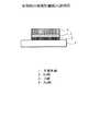
ここで、図2及び図3を参照して、本発明の第1の実施の形態を説明する。
なお、図2は、本発明の第1の実施の形態の製造工程の説明図であり、図においては、説明を簡単にするために、素子構造を省略して最上層のp型GaN層に対するp側電極の形成工程を示すものであり、また、図3は、本発明の第1の実施の形態の電極のオーミック性の熱処理温度(アニール処理温度)依存性の測定結果を示す図である。
【0047】
図2(a)参照
まず、p型GaN層11を有機洗浄及び酸洗浄してその表面を清浄化した後、EB(電子ビーム)蒸着法を用いて、p型GaN層11上に、厚さ0.05〜0.3μm、例えば、0.3μmのNi層12をオーミックコンタクト層として堆積させる。
【0048】
次いで、N2雰囲気中で、400〜800℃、例えば、400℃で、60秒〜25分、例えば、5分間のアニール処理を施す。
このアニール処理によってNi層12の耐溶剤性、例えば、耐エッチャント性が高まる。
【0049】
図2(b)参照
次いで、同じくEB蒸着法を用いて、厚さ0.03〜0.1μm、例えば、0.05μmのTi層13、及び、厚さ0.03〜0.4μm、例えば、0.05μmのAu蒸着層14を順次堆積させる。
【0050】
図2(c)参照
次いで、電解メッキ法を用いて、Au蒸着層14上に、厚さ0.5〜5μm、例えば、2.0μmのAuメッキ層15を堆積させる。
【0051】
図2(d)参照
最後に、マスク(図示せず)を用いてシアン系エッチャントのテクニストリップ金を用いてAuメッキ層15及びAu蒸着層14を所定パターンにエッチングし、次いで、フッ素系エッチャント、例えば、0.2%フッ酸水溶液、或いは、2%バッファードフッ酸を用いてTi層13をエッチングし、次いで、硝酸水溶液、硫酸水溶液、または、塩酸水溶液、例えば、40%硝酸水溶液を用いてNi層12をエッチングすることによって、p型GaN層11に対するp側電極が完成する。
【0052】
この様な、Ni/Ti/Au構造の電極は、中間にTi層を介在させているので、従来のNi/Au構造のp側電極に比べて密着性が高まり、ボンディング圧力等の物理的な衝撃によっても剥離しにくくなり、発光半導体素子の信頼性が向上する。
【0053】
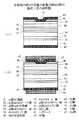
図3(a)参照
図3(a)は、400℃でアニール処理を行った場合の、p側電極の電流−電圧特性(I−V特性)の測定結果を示す図であり、低抵抗で、且つ、直線性の良好な従来のNi/Au電極と同様のオーミック特性を示している。
なお、図において、縦軸の1目盛りは50μAを表し、横軸の1目盛りは2Vを表しており、図3(b)及び(c)も同様である。
【0054】
図3(b)参照
図3(b)は、600℃でアニール処理を行った場合の、p側電極のI−V特性の測定結果を示す図であり、比較的低抵抗ではあるが、低バイアス電圧時に高抵抗化する傾向が見られる。
【0055】
図3(c)参照
図3(c)は、800℃でアニール処理を行った場合の、p側電極のI−V特性の測定結果を示す図であり、高抵抗化すると共に、低バイアス電圧側における非直線性が顕著になり、p型GaN層11とNi層12との間の合金化反応が進行していることを示している。
【0056】
したがって、800℃以上の温度によるアニール処理を行った場合には、オーミック性が劣化し、電気的特性の良好な発光半導体素子を得ることが困難になるので、アニール処理温度は800℃以下が望ましい。
【0057】
なお、Niオーミックコンタクトは、ノンアロイコンタクトであるので、400℃以下のアニール処理を施しても、そのオーミック性は400℃のアニール処理の場合と殆ど変わらない。
【0058】
また、Ni層12のアニール工程は必ずしも必須の工程ではないが、Ni層12の耐溶剤性を高めるためには、400℃以上の熱処理が必要となる。
【0059】
また、このアニール処理は、Ti層13及びAu層14の堆積前に行うことが肝要であり、Ti層13及びAu層14の堆積後に行った場合には、メタルの層間拡散、或いは、p型GaN層11への拡散等により半導体素子の電気的特性が劣化する。
【0060】
また、上記の第1の実施の形態の説明においては、メタル層の堆積手段として、EB蒸着法を用いているが、Ni層12及びAu蒸着層14についてはEB蒸着法に限られるものではなく、例えば、通常の抵抗加熱による蒸着法を用いても良いものである。
【0061】
また、上記の第1の実施の形態の説明においては、Ti層13とAu蒸着層14の厚さを0.5μm及び0.5μmにしているが、夫々、0.03μm及び0.03μmにしても良いのである。
【0062】
さらに、上記の第1の実施の形態においてはAuメッキ層15を設けているが、Auメッキ層15を用いずに、Ti層13の厚さを0.05μmにすると共に、Au蒸着層14の厚さを0.38μm以上、例えば、0.45μmに堆積するだけでも良い。
【0063】
また、上記の第1の実施の形態においては、説明を簡単にするために、p側電極を設ける半導体層をp型GaN層として説明しているが、この様な電極構造はp型Al0.1Ga0.9N層等の他のp型GaN系化合物半導体、即ち、p型AlxInyGa1-x-yN(但し、0≦x≦1,0≦y≦1)にも適用されるものである。
【0064】
次に、図4及び図5を参照して、本発明の第2の実施の形態を説明する。
なお、図4は、本発明の第2の実施の形態の製造工程の説明図であり、図においては、説明を簡単にするために、素子構造を省略してn型SiC層に対するn側電極の形成工程を示すものであり、また、図5は、本発明の第2の実施の形態の電極のオーミック性の熱処理温度(アニール処理温度)依存性の測定結果を示す図である。
【0065】
図4(a)参照
まず、n型SiC層21を有機洗浄及び酸洗浄してその表面を清浄化した後、EB(電子ビーム)蒸着法を用いて、n型SiC層21上に、厚さ0.05〜0.3μm、例えば、0.3μmのNi層22をオーミックコンタクト層として堆積させる。
【0066】
次いで、N2雰囲気中で、800〜1100℃、例えば、900℃で、30秒〜5分、例えば、5分間のアニール処理を施す。
このアニール処理によってNi層12の耐溶剤性、例えば、耐エッチャント性が高まる。
【0067】
図4(b)及び(c)参照
次いで、同じくEB蒸着法を用いて、厚さ0.03〜0.1μm、例えば、0.05μmのTi層23、及び、厚さ0.38μm以上、例えば、0.5μmのAu蒸着層24を順次堆積させる。
【0068】
図4(d)参照
最後に、マスク(図示せず)を用いてシアン系エッチャントのテクニストリップ金を用いてAu蒸着層24を所定パターンにエッチングし、次いで、フッ素系エッチャント、例えば、0.2%フッ酸水溶液、或いは、2%バッファードフッ酸を用いてTi層23をエッチングし、次いで、硝酸水溶液、硫酸水溶液、または、塩酸水溶液、例えば、40%硝酸水溶液を用いてNi層22をエッチングすることによって、n型SiC層21に対するn側電極が完成する。
【0069】
この様なn型SiC層21に対する、Ni/Ti/Au構造の電極も、中間にTi層を介在させているので、従来のNi/Au構造のn側電極に比べて密着性が高まり、ボンディング圧力等の物理的な衝撃によっても剥離しにくくなり、発光半導体素子の信頼性が向上する。
【0070】
図5(a)参照
図5(a)は、600℃でアニール処理を行った場合の、n側電極の電流−電圧特性(I−V特性)の測定結果を示す図であり、低バイアス電圧においてはほとんど電流が流れず、オーミック性を示さない。
なお、図において、縦軸の1目盛りは50μAを表し、横軸の1目盛りは2Vを表しており、図5(b)も同様である。
【0071】
図5(b)参照
図5(b)は、800℃でアニール処理を行った場合の、n側電極のI−V特性の測定結果を示す図であり、比較的低抵抗ではあるが、低バイアス電圧時に高抵抗化する傾向が見られる。
【0072】
図5(c)参照
図5(c)は、900℃でアニール処理を行った場合の、n側電極の電流−電圧特性(I−V特性)の測定結果を示す図であり、低抵抗で、且つ、直線性の良好な従来のNi/Au電極と同様のオーミック特性を示している。
なお、図において、縦軸の1目盛りは5mAを表し、横軸の1目盛りは0.2Vを表している。
【0073】
したがって、800℃未満の温度によるアニール処理を行った場合には、オーミック性が得られず、電気的特性の良好な発光半導体素子を得ることが困難になるので、アニール処理温度は800℃以上、且つ、結晶の劣化防止の観点から1100℃以下が望ましい。
【0074】
また、この場合のアニール処理も、Ti層23及びAu蒸着層24の堆積前に行うことが肝要であり、Ti層23及び蒸着Au層24の堆積後に行った場合には、メタルの層間拡散、或いは、n型SiC層21への拡散等により半導体素子の電気的特性が劣化する。
【0075】
また、この場合、Ni/Ti/Au構造を全面に蒸着したのちエッチングによりパターニングしているので、各電極の密着面積が大きくなるので、密着性が向上する。
【0076】
なお、上記の第2の実施の形態の説明においても、メタル層の堆積手段として、EB蒸着法を用いているが、Ni層22及びAu蒸着層24についてはEB蒸着法に限られるものではなく、例えば、通常の抵抗加熱による蒸着法を用いても良いものである。
【0077】
また、上記の第2の実施の形態において、アニール処理後に、酸洗浄、例えば、バッファードフッ酸による洗浄を行うことにより、Ti/Au層との密着性がさらに改善される。
【0078】
また、上記の第2の実施の形態においては、Ni層22も選択エッチングによりボンディングパッド以外の領域を除去しているが、Ni層22はエッチングせずに、Ti層23及びAu蒸着層24のみを選択的にエッチングしても良いものである。
【0079】
次に、図6及び図7を参照して、本発明の第3の実施の形態の製造工程を説明する。
図6(a)参照
まず、(0001)面、即ち、c面を主面とする六方晶の6H−SiCからなるn型SiC基板31を厚さ80〜200μm、より好適には100〜120μmになるように研磨したのち、有機洗浄及びフッ酸等による酸洗浄してその表面を清浄化した後、n型SiC基板31上に、有機金属気相成長法(MOVPE法)を用いて、例えば、厚さ50nmのn型AlGaNバッファ層32を成長させる。
【0080】
引き続いて、厚さ0.5μmのn型GaN中間層33、厚さ0.5μmで、不純物濃度が1.0×1018cm-3のn型AlGaNクラッド層34、厚さ100nmのGaN光ガイド層35、MQW活性層36、厚さ100nmのGaN光ガイド層37、厚さ0.5μmで、不純物濃度が1.0×1017cm-3のp型AlGaNクラッド層38、及び、厚さ、0.5μmで、不純物濃度が1.0×1017cm-3のp型GaNコンタクト層39を順次成長させる。
【0081】
なお、この場合のMQW活性層36は、厚さ5nmのアンドープIn0.03Ga0.97Nバリア層と厚さ5nmのアンドープIn0.15Ga0.85N井戸層を交互に成長させたものであり、また、n型AlGaNクラッド層34及びp型AlGaNクラッド層38のAl組成比は0.09である。
【0082】
図6(b)参照
次いで、EB蒸着法を用いてn型SiC基板31の裏面に厚さ0.03〜0.5μm、例えば、0.3μmのNi層42をオーミックコンタクト層として堆積させたのち、N2雰囲気中で、900〜1100℃、例えば、900℃で、30秒〜5分、例えば、5分間のアニール処理を施したのち、バッファードフッ酸或いはフッ酸水溶液を用いて洗浄する。
このアニール処理によってNi層42の耐溶剤性、例えば、耐エッチャント性が高まり、また、洗浄によって次工程で堆積させるTi/Au層との密着性が改善される。
【0083】
次いで、p型GaNコンタクト層39の表面を有機洗浄及び酸洗浄を行ったのち、p型GaNコンタクト層39上に厚さ0.2〜0.4μm、例えば、0.25μmのSiO2膜40を形成し、次いで、エッチングにより幅1〜12μmのコンタクトホール41(ストライプ状開口)を形成する。
【0084】
図7(c)参照
次いで、p型GaNコンタクト層39の露出表面を有機洗浄及び酸洗浄を行ったのち、p型GaNコンタクト層39側の全面に厚さ0.03〜0.5μm、例えば、0.3μmのNi層43をオーミックコンタクト層として堆積させる。
【0085】
次いで、N2雰囲気中で、400〜800℃、例えば、400℃で、60秒〜25分、例えば、5分間のアニール処理を行う。
このアニール処理によってNi層43の耐溶剤性、例えば、耐エッチャント性が高まる。
【0086】
図7(d)参照
次いで、同じくEB蒸着法を用いて、p型GaNコンタクト層39側に厚さ0.03〜0.1μm、例えば、0.05μmのTi層46、及び、厚さ0.38μm以上、例えば、0.45μmのAu層47を順次堆積させる。
【0087】
次いで、ボンディングパッドに対応する大きさの300μm×700μmのマスク(図示せず)を用いてシアン系エッチャントのテクニストリップ金を用いてAu層47を所定パターンにエッチングし、次いで、フッ素系エッチャント、例えば、0.2%フッ酸水溶液、或いは、2%バッファードフッ酸を用いてTi層46をエッチングし、次いで、硝酸水溶液、硫酸水溶液、或いは、塩酸水溶液、例えば、40%硝酸水溶液を用いてNi層43をエッチングすることによって、p側電極を形成する。
【0088】
次いで、同じくEB蒸着法を用いて、n型SiC基板31側に厚さ0.03〜0.1μm、例えば、0.05μmのTi層44、及び、厚さ0.38μm以上、例えば、0.45μmのAu層45を順次堆積させる。
【0089】
次いで、ボンディングパッドに対応する大きさの300μm×700μmのマスク(図示せず)を用いてシアン系エッチャントのテクニストリップ金を用いてAu層45を所定パターンにエッチングし、次いで、フッ素系エッチャント、例えば、0.2%フッ酸水溶液、或いは、2%バッファードフッ酸を用いてTi層44をエッチングすることによって、n型SiC層21に対するn側電極を形成し、最後に、適当な荷重でスクライブのキズをいれ、劈開を行うことによって青色半導体レーザが完成する。
【0090】
この様に、第3の実施の形態においては、同じ材料及び同じ工程によって形成した同じNi/Ti/Au構造の電極を用いてn側電極及びp側電極の双方を形成することができるので、製造工程を簡素化することができる。
【0091】
なお、上記の第3の実施の形態におけるp側電極は、上記の第1の実施の形態及びその変形例によって構成しても良く、また、n側電極は、上記の第2の実施の形態及びその変形例によって構成しても良い。
【0092】
また、この第3の実施の形態においては、アニール処理温度の関係から、n型SiC基板31に対してNi層42を形成したのち、p型GaNコンタクト層39に対するNi層43形成することが必須であるが、Ti層44/Au層45及びTi層46/Au層47の形成順序及びパターニング順序は適宜変更し得るものである。
【0093】
例えば、上記の図7(c)の様にn型SiC基板とp型GaNコンタクト層にNi層を形成したのち、n型SiC基板とp型GaNコンタクト層の双方にTi/Au層を順次形成し、次いで、n側電極及びp側電極をボンディングパッドに相当する大きさにエッチングしても良く、n側電極及びp側電極のどちらのボンディングパッドを先に形成しても良いものである。
【0094】
次に、図8を参照して本発明の第4の実施の形態を説明するが、オーバーフロー防止層を設ける工程、及び、リッジを構成する工程を加える以外は上記の第3の実施の形態と同様である。
図8参照
まず、n型SiC基板31上に、有機金属気相成長法(MOVPE法)を用いて、n型AlGaNバッファ層32、n型GaN中間層33、n型AlGaNクラッド層34、GaN光ガイド層35、MQW活性層36、オーバーフロー防止層となるp型AlGaN層48、GaN光ガイド層37、p型AlGaNクラッド層38、及び、p型GaNコンタクト層39を順次成長させる。
【0095】
次いで、CHF3を用いたドライ・エッチングによって、p型GaNコンタクト層39及びp型AlGaNクラッド層38を選択的にエッチングしてリッジ49を形成する。
【0096】
後は、第3の実施の形態と同様に、EB蒸着法を用いてn型SiC基板31の裏面にNi層42を堆積させたのち、N2雰囲気中でアニール処理を施したのち、バッファードフッ酸或いはフッ酸水溶液を用いて洗浄する。
【0097】
次いで、p型GaNコンタクト層39及びp型AlGaNクラッド層38の露出表面を有機洗浄及び酸洗浄を行ったのち、全面にSiO2膜40を形成し、次いで、エッチングによりコンタクトホール41(ストライプ状開口)を形成し、次いで、p型GaNコンタクト層39の露出表面を有機洗浄及び酸洗浄を行ったのち、p型GaNコンタクト層39側の全面にNi層43を堆積させる。
【0098】
次いで、N2雰囲気中でアニール処理を行ったのち、同じくEB蒸着法を用いて、p型GaNコンタクト層39側にTi層46及びAu層47を順次堆積させ、次いで、ボンディングパッドに対応する大きさの300μm×700μmのマスクを用いてAu層47、Ti層46、及び、Ni層43を順次エッチングすることによってp側電極を形成する。
【0099】
次いで、同じくEB蒸着法を用いて、n型SiC基板31側にTi層44及び、Au層45を順次堆積させたのち、ボンディングパッドに対応する大きさの300μm×700μmのマスクを用いて、Au層45及びTi層44を順次エッチングすることによって、n型SiC層31に対するn側電極を形成し、最後に、適当な荷重でスクライブのキズをいれ、劈開を行うことによって青色半導体レーザが完成する。
【0100】
以上、本発明の各実施の形態を説明してきた様に、本発明の半導体装置の主な対象は、半導体レーザ或いは発光ダイオード等の発光半導体素子であるが、本発明は、必ずしも発光半導体素子に限られるものではなく、GaN系化合物半導体を用いた他の非発光性の半導体素子にも適用されるものであり、また、SiCのみを用いた半導体装置、例えば、SiC青色発光ダイオードにも適用されるものである。
【0101】
【発明の効果】
本発明によれば、GaN系化合物半導体からなる半導体装置のp側電極及びn側電極を、Ni/Ti/Au構造としたので、電気的特性を損なうことなく密着性が向上し、電極の剥離が防止されるので、GaN系化合物半導体装置の信頼性向上に寄与し、ひいては、青色半導体レーザや青色発光ダイオードの実用化に寄与するところが大きい。
【図面の簡単な説明】
【図1】本発明の原理的構成の説明図である。
【図2】本発明の第1の実施の形態の製造工程の説明図である。
【図3】本発明の第1の実施の形態の電極のオーミック性の熱処理温度依存性の説明図である。
【図4】本発明の第2の実施の形態の製造工程の説明図である。
【図5】本発明の第2の実施の形態の電極のオーミック性の熱処理温度依存性の説明図である。
【図6】本発明の第3の実施の形態の途中までの製造工程の説明図である。
【図7】本発明の第3の実施の形態の図6以降の製造工程の説明図である。
【図8】本発明の第4の実施の形態の説明図である。
【図9】従来の短波長発光素子の説明図である。
【符号の説明】
1 半導体層
2 Ni層
3 Ti層
4 Au層
11 p型GaN層
12 Ni層
13 Ti層
14 Au蒸着層
15 Auメッキ層
21 n型SiC層
22 Ni層
23 Ti層
24 Au蒸着層
31 n型SiC基板
32 n型AlGaNバッファ層
33 n型GaN中間層
34 n型AlGaNクラッド層
35 GaN光ガイド層
36 MQW活性層
37 GaN光ガイド層
38 p型AlGaNクラッド層
39 p型GaNコンタクト層
40 SiO2膜
41 コンタクトホール
42 Ni層
43 Ni層
44 Ti層
45 Au層
46 Ti層
47 Au層
48 p型AlGaN層
49 リッジ
51 サファイア基板
52 GaN低温バッファ層
53 n型Al0.1Ga0.9Nクラッド層
54 n型GaN光ガイド層
55 In0.1Ga0.9N活性層
56 p型GaN光ガイド層
57 p型Al0.1Ga0.9Nクラッド層
58 p型GaNコンタクト層
59 Ti/Au電極
60 Ni/Au電極[0001]
BACKGROUND OF THE INVENTION
The present invention relates to a semiconductor device and a manufacturing method thereof, and more particularly to an ohmic electrode structure of a short wavelength light emitting element made of a GaN-based compound semiconductor and a semiconductor device characterized by its manufacturing process and a manufacturing method thereof.
[0002]
[Prior art]
In recent years, a short wavelength semiconductor laser having a wavelength from blue to the near ultraviolet region has been actively developed, and a GaN-based compound semiconductor has a direct transition type and a band gap changes from 1.95 to 6 eV. Researched as a material for semiconductor lasers.
[0003]
In particular, with the announcement of GaN high-brightness LEDs by Nichia three years ago, GaN-based compound semiconductors with excellent environmental resistance regarding the reliability that has become a bottleneck in the ZnSe system have been reviewed. (See S. Nakamura et al., Japane Journal of Applied Physics,
[0004]
Since this GaN compound semiconductor is a wurtzite compound semiconductor, it is epitaxially grown on a hexagonal sapphire substrate or 6H-SiC substrate having a similar crystal structure by using the MOVPE method (metal organic chemical vapor deposition method). Accordingly, a conventional short wavelength light emitting device will be described with reference to FIG.
[0005]
See FIG.
First, n-type Al is formed on a
[0006]
When an n-type 6H—SiC substrate is used instead of the sapphire substrate, a Ni / Au electrode or the like is formed on the back surface of the n-type SiC substrate.
[0007]
[Problems to be solved by the invention]
However, in the case of a conventional short wavelength light emitting device, Ni / Au electrodes for the p-type semiconductor layer and the n-type semiconductor layer (if necessary, for example, JP-A-3-46379, JP-A-8-316529) Or, see JP-A-61-272968), there is a problem that the adhesion between the Ni layer serving as an ohmic contact electrode and the Au layer serving as a bonding metal layer is poor, and the electrode is easily peeled off.
[0008]
In addition to the Ni / Au electrode, an electrode having a Ti / Ni / Au structure is also proposed (if necessary, JP-A-61-43461, JP-A-55-115392, or JP-A-57-15446). The Ti diffuses by annealing treatment, and the adhesion between the Ni layer and the Au layer is improved, but the adhesion is better than the method of forming a Ti layer that can directly control the film thickness. There is a problem that the reliability and reliability are inferior.
[0009]
An electrode having a Ni / Ti / Pt / Au structure has also been proposed (see JP-A-61-69148 or JP-A-8-250704 if necessary). Although the adhesiveness of Pt is good, there is a problem that the adhesiveness of Pt / Au is poor.
[0010]
Further, in the case of n-type SiC or p-type AlInGaN, the above Ti / Ni / Au or Ni.Cr/(Ti)/Au (for example, JP-A-61-61) is used as compared with the Ni layer as a contact layer. No. 272968) or Au.Ge/Ni/Au (for example, see Japanese Patent Laid-Open No. 5-291609) has a problem not only in adhesion but also in ohmic properties.
[0011]
Therefore, the present invention provides p-type AlxInyGa1-xyIt aims at preventing peeling of the electrode provided in N and n-type SiC.
[0012]
[Means for Solving the Problems]
FIG. 1 is an explanatory view of the principle configuration of the present invention. Means for solving the problems in the present invention will be described with reference to FIG.
See Figure 1
(1) The present invention provides a semiconductor device,An
[0017]
As described above, the
[0018]
(2In addition, the present invention provides the above (1), N-type SiC constitutes an n-type semiconductor layer of the light-emitting semiconductor element.
[0019]
The n-side electrode for n-type SiC having such a configuration is suitable as an n-side electrode for a light-emitting semiconductor element such as a blue semiconductor laser, a blue light-emitting diode, or a SiC blue light-emitting diode using n-type SiC as a substrate.
[0020]
(3The present invention is the above (1) Or (2P-type Al as the uppermost layer of the laminated structure provided on the n-type SiCxInyGa1-xyN (provided that 0 ≦ x ≦ 1, 0 ≦ y ≦ 1) and this p-type AlxInyGa1-xyA
[0021]
As described above, for a GaN-based semiconductor device using an n-type SiC substrate, an electrode having good adhesion can be constituted by the same Ni / Ti / Au structure electrode as the n-side electrode and the p-side electrode. it can.
[0024]
(4In addition, the present inventionThe Ni
[0025]
As described above, when the electrode having the
[0027]
The electrode having such a structure is p-type Al.xInyGa1-xySuitable for N, p-type AlxInyGa1-xySince the
[0029]
When the annealing temperature exceeds 800 ° C, p-type AlxInyGa1-xySince the alloying reaction between N and
[0030]
(5In addition, the present invention provides the above(4)In p-type AlxInyGa1-xyN1 constitutes a p-type semiconductor layer of the light-emitting semiconductor element.
[0031]
By adopting the manufacturing process of the p-side electrode having such a configuration as the manufacturing process of the p-side electrode of a light-emitting semiconductor element such as a blue semiconductor laser or a blue light-emitting diode, peeling of the p-side electrode of the light-emitting semiconductor element is prevented. Reliability.
[0032]
(6In addition, the present inventionA method of manufacturing a semiconductor device, characterized in that after the
[0033]
Such an electrode manufacturing method is suitable for n-type SiC, and the
[0034]
(7In addition, the present invention provides the above (6), The annealing temperature is 800 ° C. or higher.
[0035]
If the annealing temperature is less than 800 ° C., good ohmic properties cannot be obtained for the n-side electrode. Therefore, the temperature is desirably 800 ° C. or higher, and 1100 ° C. or lower from the viewpoint of preventing crystal deterioration. Is desirable.
[0036]
(8In addition, the present invention provides the above (7), After the annealing treatment, the treatment with a hydrofluoric acid solvent is performed before the Ti layer is deposited.
[0037]
In this way, after the annealing treatment, before the Ti layer is deposited, the
[0038]
(9In addition, the present invention provides the above (6) To (8), The n-type SiC constitutes an n-type semiconductor layer of the light-emitting semiconductor element.
[0039]
By adopting the manufacturing process of the n-side electrode having such a configuration as the manufacturing process of the n-side electrode of a light emitting semiconductor element such as a blue semiconductor laser, a blue light emitting diode, or a SiC light emitting diode using n-type SiC as a substrate. The n-side electrode of the light emitting semiconductor element can be prevented from being peeled off and the reliability can be improved.
[0040]
(10In addition, the present invention provides the above (6) To (9), P-type Al on n-type SiC.xInyGa1-xyA multi-layer structure having N (where 0 ≦ x ≦ 1, 0 ≦ y ≦ 1) as the uppermost layer is formed, and this p-type AlxInyGa1-xyAfter the
[0041]
The electrode manufacturing process as described above is applied to both an n-side electrode and a p-side electrode for a semiconductor device in which a GaN-based semiconductor is stacked on an n-type SiC substrate, so that an n-side electrode and a p-side without separation are provided. An electrode can be constructed.
[0042]
(11In addition, the present invention provides the above (10), After providing an n-side electrode for n-type SiC, p-type AlxInyGa1-xyA p-side electrode for N is formed.
[0043]
As mentioned above, p-type AlxInyGa1-xySince the annealing temperature for N is 800 ° C. or lower and the annealing temperature for n-type SiC is 800 ° C. or higher, it is necessary to form the p-side electrode after forming the n-side electrode.
[0044]
(12In addition, the present invention provides the above (4) To (11), At least the
[0045]
Thus, after providing the
[0046]
DETAILED DESCRIPTION OF THE INVENTION
Here, the first embodiment of the present invention will be described with reference to FIG. 2 and FIG.
FIG. 2 is an explanatory diagram of the manufacturing process according to the first embodiment of the present invention. In the figure, for simplicity of explanation, the element structure is omitted and the uppermost p-type GaN layer is illustrated. The p-side electrode forming process is shown, and FIG. 3 is a diagram showing the measurement results of the ohmic heat treatment temperature (annealing temperature) dependence of the electrode according to the first embodiment of the present invention. .
[0047]
See Fig. 2 (a)
First, after cleaning the surface of the p-
[0048]
Then N2In the atmosphere, annealing is performed at 400 to 800 ° C., for example, 400 ° C., for 60 seconds to 25 minutes, for example, 5 minutes.
This annealing process increases the solvent resistance of the
[0049]
Refer to FIG.
Then, using the same EB vapor deposition method, a
[0050]
Refer to FIG.
Next, an
[0051]
Refer to FIG.
Finally, the
[0052]
Such a Ni / Ti / Au structure electrode has a Ti layer interposed therebetween, so that the adhesion is higher than that of the conventional Ni / Au structure p-side electrode, and the physical properties such as bonding pressure are increased. It becomes difficult to peel off even by impact, and the reliability of the light emitting semiconductor element is improved.
[0053]
See Fig. 3 (a)
FIG. 3A is a diagram showing the measurement result of the current-voltage characteristics (IV characteristics) of the p-side electrode when annealing is performed at 400 ° C., which has low resistance and linearity. It shows ohmic characteristics similar to those of a good conventional Ni / Au electrode.
In the figure, one scale on the vertical axis represents 50 μA, one scale on the horizontal axis represents 2 V, and the same applies to FIGS. 3B and 3C.
[0054]
Refer to FIG.
FIG. 3B is a diagram showing the measurement results of the IV characteristics of the p-side electrode when annealing is performed at 600 ° C., and the resistance is relatively low but the resistance is increased at a low bias voltage. The tendency to do is seen.
[0055]
Refer to FIG.
FIG. 3C is a diagram showing the measurement result of the IV characteristic of the p-side electrode when the annealing process is performed at 800 ° C. The resistance is increased and the non-linearity on the low bias voltage side is also shown. It becomes prominent, indicating that the alloying reaction between the p-
[0056]
Therefore, when annealing is performed at a temperature of 800 ° C. or higher, ohmic properties are deteriorated and it becomes difficult to obtain a light-emitting semiconductor element having good electrical characteristics. Therefore, the annealing temperature is desirably 800 ° C. or lower. .
[0057]
Since the Ni ohmic contact is a non-alloy contact, even if annealing at 400 ° C. or lower is performed, the ohmic property is almost the same as in the case of annealing at 400 ° C.
[0058]
In addition, although the annealing process of the
[0059]
In addition, it is important that this annealing process be performed before the deposition of the
[0060]
In the description of the first embodiment, the EB vapor deposition method is used as the metal layer deposition means. However, the
[0061]
In the description of the first embodiment, the thicknesses of the
[0062]
Furthermore, although the
[0063]
In the first embodiment, the semiconductor layer on which the p-side electrode is provided is described as a p-type GaN layer for the sake of simplicity, but such an electrode structure has a p-type Al structure.0.1Ga0.9Other p-type GaN compound semiconductors such as N-layer, ie p-type AlxInyGa1-xyThis applies also to N (however, 0 ≦ x ≦ 1, 0 ≦ y ≦ 1).
[0064]
Next, a second embodiment of the present invention will be described with reference to FIGS.
FIG. 4 is an explanatory diagram of the manufacturing process according to the second embodiment of the present invention. In the figure, for simplicity of explanation, the element structure is omitted and the n-side electrode for the n-type SiC layer is shown. FIG. 5 is a diagram showing a measurement result of the ohmic heat treatment temperature (annealing temperature) dependency of the electrode according to the second embodiment of the present invention.
[0065]
See Fig. 4 (a)
First, after cleaning the surface of the n-
[0066]
Then N2In the atmosphere, annealing is performed at 800 to 1100 ° C., for example, 900 ° C., for 30 seconds to 5 minutes, for example, 5 minutes.
This annealing process increases the solvent resistance of the
[0067]
See FIG. 4 (b) and (c).
Next, similarly using the EB vapor deposition method, a
[0068]
Refer to FIG.
Finally, the Au
[0069]
Since the Ni / Ti / Au structure electrode for such an n-
[0070]
Refer to FIG.
FIG. 5A is a diagram showing the measurement result of the current-voltage characteristics (IV characteristics) of the n-side electrode when annealing is performed at 600 ° C., and current flows almost at a low bias voltage. It does not show ohmic properties.
In the figure, one scale on the vertical axis represents 50 μA, one scale on the horizontal axis represents 2 V, and the same applies to FIG.
[0071]
Refer to FIG.
FIG. 5B is a diagram showing a measurement result of the IV characteristic of the n-side electrode when annealing is performed at 800 ° C., which has a relatively low resistance but has a high resistance at a low bias voltage. The tendency to do is seen.
[0072]
Refer to FIG.
FIG. 5 (c)9It is a figure which shows the measurement result of the electric current-voltage characteristic (IV characteristic) of an n side electrode at the time of performing an annealing process at 00 degreeC, and is low resistance and the conventional Ni / Au with favorable linearity It shows the same ohmic characteristics as the electrode.
In the figure, one scale on the vertical axis represents 5 mA, and one scale on the horizontal axis represents 0.2V.
[0073]
Therefore, when an annealing process is performed at a temperature lower than 800 ° C., ohmic properties cannot be obtained, and it becomes difficult to obtain a light-emitting semiconductor element with good electrical characteristics. In addition, 1100 ° C. or less is desirable from the viewpoint of preventing crystal deterioration.
[0074]
In addition, it is important that the annealing process in this case also be performed before the deposition of the
[0075]
In this case, since the Ni / Ti / Au structure is deposited on the entire surface and then patterned by etching, the adhesion area of each electrode is increased, and the adhesion is improved.
[0076]
In the description of the second embodiment, the EB vapor deposition method is used as the metal layer deposition means. However, the
[0077]
In the second embodiment, the adhesion with the Ti / Au layer is further improved by performing acid cleaning, for example, cleaning with buffered hydrofluoric acid, after the annealing treatment.
[0078]
In the second embodiment, the
[0079]
Next, with reference to FIG.6 and FIG.7, the manufacturing process of the 3rd Embodiment of this invention is demonstrated.
See Fig. 6 (a)
First, after polishing an n-
[0080]
Subsequently, an n-type GaN
[0081]
In this case, the MQW
[0082]
Refer to FIG.
Next, after depositing an
This annealing process increases the solvent resistance of the
[0083]
Next, the surface of the p-type
[0084]
See Fig. 7 (c)
Next, the exposed surface of the p-type
[0085]
Then N2In the atmosphere, annealing is performed at 400 to 800 ° C., for example, 400 ° C., for 60 seconds to 25 minutes, for example, 5 minutes.
This annealing process increases the solvent resistance of the
[0086]
Refer to FIG.
Next, similarly using the EB vapor deposition method, the
[0087]
Next, the
[0088]
Next, similarly, using the EB vapor deposition method, the
[0089]
Next, the
[0090]
Thus, in the third embodiment, both the n-side electrode and the p-side electrode can be formed using the same Ni / Ti / Au structure electrode formed by the same material and the same process. The manufacturing process can be simplified.
[0091]
Note that the p-side electrode in the third embodiment may be configured by the first embodiment and its modification, and the n-side electrode is the second embodiment. And you may comprise by the modification.
[0092]
In the third embodiment, it is essential to form the
[0093]
For example, after forming the Ni layer on the n-type SiC substrate and the p-type GaN contact layer as shown in FIG. 7C, the Ti / Au layer is sequentially formed on both the n-type SiC substrate and the p-type GaN contact layer. Then, the n-side electrode and the p-side electrode may be etched to a size corresponding to the bonding pad, and either the n-side electrode or the p-side electrode may be formed first.
[0094]
Next, a fourth embodiment of the present invention will be described with reference to FIG. 8, except that a step of providing an overflow prevention layer and a step of forming a ridge are added. It is the same.
See FIG.
First, an n-type
[0095]
Then CHFThreeThe p-type
[0096]
After that, similarly to the third embodiment, an
[0097]
Next, the exposed surfaces of the p-type
[0098]
Then N2After annealing in the atmosphere, the
[0099]
Next, the
[0100]
As described above, as described in each embodiment of the present invention, the main object of the semiconductor device of the present invention is a light-emitting semiconductor element such as a semiconductor laser or a light-emitting diode. The present invention is not limited, and can be applied to other non-emissive semiconductor elements using a GaN-based compound semiconductor, and also applied to a semiconductor device using only SiC, for example, a SiC blue light emitting diode. Is.
[0101]
【The invention's effect】
According to the present invention, since the p-side electrode and the n-side electrode of the semiconductor device made of a GaN-based compound semiconductor have a Ni / Ti / Au structure, the adhesion is improved without impairing the electrical characteristics, and the electrode is peeled off. Therefore, it contributes to improving the reliability of the GaN-based compound semiconductor device, and in turn contributes to the practical use of blue semiconductor lasers and blue light emitting diodes.
[Brief description of the drawings]
FIG. 1 is an explanatory diagram of a basic configuration of the present invention.
FIG. 2 is an explanatory diagram of a manufacturing process according to the first embodiment of this invention.
FIG. 3 is an explanatory diagram of the heat treatment temperature dependence of the ohmic property of the electrode according to the first embodiment of the present invention.
FIG. 4 is an explanatory diagram of a manufacturing process according to the second embodiment of this invention.
FIG. 5 is an explanatory diagram of the heat treatment temperature dependence of the ohmic property of the electrode according to the second embodiment of the present invention.
FIG. 6 is an explanatory diagram of the manufacturing process up to the middle of the third embodiment of the present invention.
FIG. 7 is an explanatory diagram of the manufacturing process after FIG. 6 according to the third embodiment of the present invention.
FIG. 8 is an explanatory diagram of a fourth embodiment of the present invention.
FIG. 9 is an explanatory diagram of a conventional short wavelength light emitting device.
[Explanation of symbols]
1 Semiconductor layer
2 Ni layer
3 Ti layer
4 Au layer
11 p-type GaN layer
12 Ni layer
13 Ti layer
14 Au evaporated layer
15 Au plating layer
21 n-type SiC layer
22 Ni layer
23 Ti layer
24 Au evaporated layer
31 n-type SiC substrate
32 n-type AlGaN buffer layer
33 n-type GaN intermediate layer
34 n-type AlGaN cladding layer
35 GaN light guide layer
36 MQW active layer
37 GaN light guide layer
38 p-type AlGaN cladding layer
39 p-type GaN contact layer
40 SiO2film
41 Contact hole
42 Ni layer
43 Ni layer
44 Ti layer
45 Au layer
46 Ti layer
47 Au layer
48 p-type AlGaN layer
49 Ridge
51 Sapphire substrate
52 GaN low temperature buffer layer
53 n-type Al0.1Ga0.9N clad layer
54 n-type GaN optical guide layer
55 In0.1Ga0.9N active layer
56 p-type GaN optical guide layer
57 p-type Al0.1Ga0.9N clad layer
58 p-type GaN contact layer
59 Ti / Au electrode
60 Ni / Au electrode
Claims (12)
Translated fromJapanesePriority Applications (1)
| Application Number | Priority Date | Filing Date | Title |
|---|---|---|---|
| JP20773797AJP3965610B2 (en) | 1997-08-01 | 1997-08-01 | Semiconductor device and manufacturing method thereof |
Applications Claiming Priority (1)
| Application Number | Priority Date | Filing Date | Title |
|---|---|---|---|
| JP20773797AJP3965610B2 (en) | 1997-08-01 | 1997-08-01 | Semiconductor device and manufacturing method thereof |
Publications (3)
| Publication Number | Publication Date |
|---|---|
| JPH1154843A JPH1154843A (en) | 1999-02-26 |
| JPH1154843A5 JPH1154843A5 (en) | 2005-04-21 |
| JP3965610B2true JP3965610B2 (en) | 2007-08-29 |
Family
ID=16544711
Family Applications (1)
| Application Number | Title | Priority Date | Filing Date |
|---|---|---|---|
| JP20773797AExpired - LifetimeJP3965610B2 (en) | 1997-08-01 | 1997-08-01 | Semiconductor device and manufacturing method thereof |
Country Status (1)
| Country | Link |
|---|---|
| JP (1) | JP3965610B2 (en) |
Cited By (1)
| Publication number | Priority date | Publication date | Assignee | Title |
|---|---|---|---|---|
| US10679861B2 (en) | 2017-03-24 | 2020-06-09 | Toyoda Gosei Co., Ltd. | Manufacturing method of a semiconductor device |
Families Citing this family (13)
| Publication number | Priority date | Publication date | Assignee | Title |
|---|---|---|---|---|
| DE19954319C1 (en) | 1999-11-11 | 2001-05-03 | Vishay Semiconductor Gmbh | Production of multilayered contact electrodes used in diodes comprises applying a first metallizing layer, heat treating and applying a second metallizing layer over the first layer |
| JP3912044B2 (en)* | 2001-06-06 | 2007-05-09 | 豊田合成株式会社 | Method for manufacturing group III nitride compound semiconductor light emitting device |
| US7518163B2 (en)* | 2003-12-17 | 2009-04-14 | Showa Denko K.K. | Gallium nitride-based compound semiconductor light-emitting device and negative electrode thereof |
| JP2005203765A (en)* | 2003-12-17 | 2005-07-28 | Showa Denko Kk | Semiconductor light emitting element of gallium nitride compound and its negative electrode |
| CN1305186C (en)* | 2003-12-29 | 2007-03-14 | 中国科学院半导体研究所 | Method for manufacturing electric pumping edge emission semiconductor micro cavity laser |
| JP4030556B2 (en) | 2005-06-30 | 2008-01-09 | シャープ株式会社 | Nitride semiconductor laser device and nitride semiconductor laser device |
| JP2007059719A (en)* | 2005-08-25 | 2007-03-08 | Nippon Telegr & Teleph Corp <Ntt> | Nitride semiconductor |
| JP2007188928A (en)* | 2006-01-11 | 2007-07-26 | Matsushita Electric Ind Co Ltd | Nitride semiconductor light emitting device |
| DE102007012359A1 (en)* | 2007-03-14 | 2008-09-25 | Fupo Electronics Corp. | Epitaxial LED chip bond pad manufacturing method, involves subjecting surface of metal layer by surface treatment i.e. surface cleaning, to increase adhesive strength, and separating metal layer from surface of another layer |
| JP2007173866A (en)* | 2007-03-16 | 2007-07-05 | Sumitomo Electric Ind Ltd | Semiconductor light emitting device |
| JP2009182217A (en)* | 2008-01-31 | 2009-08-13 | Sumitomo Electric Ind Ltd | Semiconductor device and manufacturing method thereof |
| JP6111818B2 (en) | 2013-04-24 | 2017-04-12 | 三菱電機株式会社 | Semiconductor device and method for manufacturing semiconductor device |
| WO2021157027A1 (en)* | 2020-02-06 | 2021-08-12 | 三菱電機株式会社 | Semiconductor device and method for producing same |
- 1997
- 1997-08-01JPJP20773797Apatent/JP3965610B2/ennot_activeExpired - Lifetime
Cited By (1)
| Publication number | Priority date | Publication date | Assignee | Title |
|---|---|---|---|---|
| US10679861B2 (en) | 2017-03-24 | 2020-06-09 | Toyoda Gosei Co., Ltd. | Manufacturing method of a semiconductor device |
Also Published As
| Publication number | Publication date |
|---|---|
| JPH1154843A (en) | 1999-02-26 |
Similar Documents
| Publication | Publication Date | Title |
|---|---|---|
| JP3965610B2 (en) | Semiconductor device and manufacturing method thereof | |
| US20100059790A1 (en) | Nitride-based semiconductor device and method of manufacturing the same | |
| US7964424B2 (en) | Method for manufacturing nitride semiconductor light-emitting element | |
| KR20100064052A (en) | Semiconductor light emiitting device | |
| US8686442B2 (en) | Nitride semiconductor light emitting device and method of manufacturing the same | |
| JP4046582B2 (en) | Nitride-based semiconductor light-emitting device and method for forming the same | |
| US6744075B2 (en) | Nitride-based semiconductor light-emitting device and method of forming the same | |
| JP3693142B2 (en) | Semiconductor laser device and manufacturing method thereof | |
| JP2000299528A (en) | Semiconductor laser and manufacture thereof | |
| JP2004022989A (en) | Nitride semiconductor laser and method of manufacturing the same | |
| US8000364B2 (en) | Nitride semiconductor light emitting device and method of manufacturing the same | |
| JP2006066660A (en) | Nitride semiconductor laser device and manufacturing method thereof | |
| JP4601391B2 (en) | Nitride semiconductor device and manufacturing method thereof | |
| JP4111696B2 (en) | Nitride semiconductor laser device | |
| JP2007184644A (en) | Semiconductor device and manufacturing method thereof | |
| JP2009094108A (en) | Manufacturing method of GaN-based LED element | |
| JP4136746B2 (en) | Method of forming nitride semiconductor and nitride semiconductor device | |
| JPH11340569A (en) | Formation of electrode of semiconductor element and its structure | |
| KR101124470B1 (en) | Semiconductor light emitting device | |
| JP2010021206A (en) | Semiconductor light-emitting element | |
| KR102051477B1 (en) | Method of manufacturing semiconductor light emitting device | |
| JP4799582B2 (en) | Manufacturing method of semiconductor device | |
| JPH1140890A (en) | Low-resistance gallium nitride light-emitting device and manufacture thereof | |
| JP4994656B2 (en) | Method for manufacturing optical semiconductor element | |
| JP3948949B2 (en) | Method for manufacturing nitride-based semiconductor light-emitting device |
Legal Events
| Date | Code | Title | Description |
|---|---|---|---|
| A521 | Written amendment | Free format text:JAPANESE INTERMEDIATE CODE: A523 Effective date:20040611 | |
| A621 | Written request for application examination | Free format text:JAPANESE INTERMEDIATE CODE: A621 Effective date:20040611 | |
| A131 | Notification of reasons for refusal | Free format text:JAPANESE INTERMEDIATE CODE: A131 Effective date:20061226 | |
| A521 | Written amendment | Free format text:JAPANESE INTERMEDIATE CODE: A523 Effective date:20070220 | |
| TRDD | Decision of grant or rejection written | ||
| A01 | Written decision to grant a patent or to grant a registration (utility model) | Free format text:JAPANESE INTERMEDIATE CODE: A01 Effective date:20070515 | |
| A61 | First payment of annual fees (during grant procedure) | Free format text:JAPANESE INTERMEDIATE CODE: A61 Effective date:20070517 | |
| R150 | Certificate of patent or registration of utility model | Free format text:JAPANESE INTERMEDIATE CODE: R150 | |
| FPAY | Renewal fee payment (event date is renewal date of database) | Free format text:PAYMENT UNTIL: 20110608 Year of fee payment:4 | |
| FPAY | Renewal fee payment (event date is renewal date of database) | Free format text:PAYMENT UNTIL: 20120608 Year of fee payment:5 | |
| FPAY | Renewal fee payment (event date is renewal date of database) | Free format text:PAYMENT UNTIL: 20120608 Year of fee payment:5 | |
| FPAY | Renewal fee payment (event date is renewal date of database) | Free format text:PAYMENT UNTIL: 20130608 Year of fee payment:6 | |
| FPAY | Renewal fee payment (event date is renewal date of database) | Free format text:PAYMENT UNTIL: 20140608 Year of fee payment:7 | |
| EXPY | Cancellation because of completion of term |